SiGe field effect transistors - UNISA · SiGe field effect transistors Y.H. Xie ... interested in...
33
SiGe field effect transistors Y.H. Xie Bell Laboratories, Lucent Technologies, 600 Mountain Avenue; Murray Hill, NJ 07974, USA Abstract Starting from a brief review of the basics of FETs and BJTs, we discuss typical applications of the two types of transistors, which is followed by a FET performance analysis including the transconductance, speed, power consumption, and packing density. These sections form the foundations for the understanding of the pros and cons of strained SiGe FETs. Based on this foundation, we scrutinize the perceived advantages of using SiGe, review the array of SiGe FET structures, and look at material and processing challenges. # 1999 Elsevier Science S.A. All rights reserved. 1. Overview 1.1. Historic perspective in the understanding of SiGe/Si material The first research effort aimed at the growth of epitaxial SiGe thin films on Si substrates can be dated back to 1975, when Kasper et al. [1] published their results of Si/Ge superlattice grown on Si substrates using molecular beam epitaxy (MBE), which they termed UHV epitaxy. Publication in this field was scarce for the next 8 years as the electronic and optical properties measurable in the material system were dominated by material defects, especially dislocations derived from the large (4%) lattice mismatch between Ge and Si. In 1983, Bean and coworkers [2,3] conducted systematic studies on the material issues, and outlined the parameter space in which high quality, pseudomorphic SiGe thin films could be grown on Si substrates. Such improvement in material quality brought about a rapid expansion of the field. Electronic transport study [4] was followed by an array of demonstrative devices ranging from field effect transistors (FETs) [5,6] to photodetectors [7,8]. Heterojunction bipolar transistors (HBTs), have been carried one step beyond the demonstrative devices stage. Significant effort has been put into integrating HBRs with the integrated circuit technology [9,10,11]. In the meantime, a systematic understanding of the energy band structure [12], fundamental electronic properties [13], and material issues [14,15] has been developed. The introduction of compositional graded, related SiGe buffer layers [16] opened up another dimension in this arena. One can now adjust the strain in a SiGe film from compression all the way to tension, while maintaining the threading dislocation density at the surface of the buffer layer to below 10 6 cm 2 . Such relaxed buffer layers allowed the fabrication of high mobility two dimensional electron gas (2DEG) and hole gas (2DHG) with the highest mobility ever reported on Si substrates [17–20]. Materials Science and Engineering, 25 (1999) 89–121 0927-796X/99/$ – see front matter # 1999 Elsevier Science S.A. All rights reserved. PII:S0927-796X(99)00002-9
Transcript of SiGe field effect transistors - UNISA · SiGe field effect transistors Y.H. Xie ... interested in...
SiGe field effect transistors
Y.H. XieBell Laboratories, Lucent Technologies, 600 Mountain Avenue; Murray Hill, NJ 07974, USA
Abstract
Starting from a brief review of the basics of FETs and BJTs, we discuss typical applications of the two typesof transistors, which is followed by a FET performance analysis including the transconductance, speed, powerconsumption, and packing density. These sections form the foundations for the understanding of the pros and cons ofstrained SiGe FETs. Based on this foundation, we scrutinize the perceived advantages of using SiGe, review thearray of SiGe FET structures, and look at material and processing challenges. # 1999 Elsevier Science S.A.All rights reserved.
1. Overview
1.1. Historic perspective in the understanding of SiGe/Si material
The first research effort aimed at the growth of epitaxial SiGe thin films on Si substrates can bedated back to 1975, when Kasper et al. [1] published their results of Si/Ge superlattice grown on Sisubstrates using molecular beam epitaxy (MBE), which they termed UHV epitaxy. Publication in thisfield was scarce for the next 8 years as the electronic and optical properties measurable in thematerial system were dominated by material defects, especially dislocations derived from the large(4%) lattice mismatch between Ge and Si. In 1983, Bean and coworkers [2,3] conducted systematicstudies on the material issues, and outlined the parameter space in which high quality,pseudomorphic SiGe thin films could be grown on Si substrates. Such improvement in materialquality brought about a rapid expansion of the field. Electronic transport study [4] was followed byan array of demonstrative devices ranging from field effect transistors (FETs) [5,6] to photodetectors[7,8]. Heterojunction bipolar transistors (HBTs), have been carried one step beyond thedemonstrative devices stage. Significant effort has been put into integrating HBRs with theintegrated circuit technology [9,10,11]. In the meantime, a systematic understanding of the energyband structure [12], fundamental electronic properties [13], and material issues [14,15] has beendeveloped. The introduction of compositional graded, related SiGe buffer layers [16] opened upanother dimension in this arena. One can now adjust the strain in a SiGe film from compression allthe way to tension, while maintaining the threading dislocation density at the surface of the bufferlayer to below 106 cmÿ2. Such relaxed buffer layers allowed the fabrication of high mobility twodimensional electron gas (2DEG) and hole gas (2DHG) with the highest mobility ever reported on Sisubstrates [17±20].
Materials Science and Engineering, 25 (1999) 89±121
0927-796X/99/$ ± see front matter # 1999 Elsevier Science S.A. All rights reserved.
PII: S 0 9 2 7 - 7 9 6 X ( 9 9 ) 0 0 0 0 2 - 9

1.2. The natural next step
Based on all the studies done to date, the knowledge about SiGe/Si materials can be summarizedas follows: SiGe/Si interface is the highest quality crystalline±crystalline heterointerface available onSi substrates. Strain determines the energy band edge lineup at these heterointerfaces, allowingelectron confinement (for two dimensional electron gas (2DEG)) in the case of tensile strain, andhole confinement (for two dimensional hole gas (2DHG)) in the case of compressive strain. Strainalso lifts degeneracies at energy band edges, resulting in lighter effective masses in the 2D plane forboth electrons (0.19 m0) [4] and holes (<0.1 m0) [21]. The defect density in SiGe films can be madelow enough for band edge luminescence to be observed at low temperatures [22,23]. Thermallystable films of 1% strain with thickness up to 100 AÊ can be grown without the danger of havingdislocations. Given these known qualities of the material system, exploring the possibility of using itto fabricate enhanced performance FETs is the natural next step. The expected performanceenhancement comes from the lighter effective mass, reduced interval scattering, and the possibilityof having a better heterointerface than that between SiO2 and Si (amorphous±crystalline interface).All these should result in improved carrier mobility and transconductance. Furthermore, an enhancedtransconductance allows increased latitude in the design tradeoffs between FET dimensions andcircuit performance. These conjectures are scrutinized in the rest of this review.
1.3. Organization
The review is organized as follows. The basics of FETs will be presented briefly. The keyperformance metrics of FETs are then discussed with some typical applications in mind. Havingbuilt these foundations for the discussion, the perceived advantage of using SiGe is scrutinized. Theissue of process complexity, which often determines whether an invention will eventually becomepart of the VLSI technology, will be discussed. The final section presents the technologicalchallenges and future areas of research.
1.4. Targeted audience
The purpose of this review is to summarize important issues and the state of the art of SiGe/SiFETs, instead of drawing conclusions about the future of the field. It is hoped that this will be usefulto material researchers interested in the device issues related to SiGe, and device researchersinterested in finding out about materials issues pertinent to SiGe FETs.
2. Basics of field effect transistors
The term FET typically refers to a class of four-terminal devices in which the resistance of asemiconductor channel is modulated by the electric field in the direction perpendicular to that of thecurrent flow. The basic concept was proposed by Lilienfeld [24±26] in 1926, and was the firstinvention of transistors. In the first proposed FET structure, the transverse electric field modulates theconductance of majority carriers in a semiconductor channel. This is quite different from the MOSFETsused in modern integrated circuits, in which the conductance of an inversion layer (i.e. of minoritycarriers) near the SiO2/Si interface is controlled by the transverse electric field. The transistor DCcharacteristic can be satisfactorily described by knowing the distribution and transport of the minoritycarrier (either electron or hole). That is why FETs are also known as unipolar transistors.
90 Y.H. Xie / Materials Science and Engineering 25 (1999) 89±121
The past 70 years stand witness to the evolution which turned this brilliant invention into `themost abundant man-made object on this planet earth' [27]. Progress in semiconductor relatedmaterials sciences helped surmounting many of the crucial roadblocks. The first such example is thepoor quality of semiconductor/dielectric interface in the early days. Steam oxidation of Si solved thatproblem, and made the realization of the first FET possible [28]. The stability and quality of theSiO2/Si interface is the single most important reason that Si is the material of choice in the VLSItechnology. Other materials related progresses include hydrogenation, diffusion, ion implantation,and silicidation, to name a few. While a significant portion of the VLSI technology advancement inthe recent years has come from circuit design innovation and novel transistor structure design, it isimportant to remember that materials science is, and forever will be the corner stone of the integratedcircuit technology.
In this section, we will first follow through the text book derivative of the ideal MOSFETequations for both DC and AC cases. We will then discuss the non-ideal factors associated withMOSFETs in modern VLSI technology, including issues like the short channel effect and gate oxidedegradation. Depending on the degree of detail one desires to get into, there are several books whichrender excellent teaching of device physics. The three books in [29±31] are listed in the order fromintroductory to advanced. The introduction to MOSFET as well as bipolar transistor operationprinciple given below follows similar path of [29].
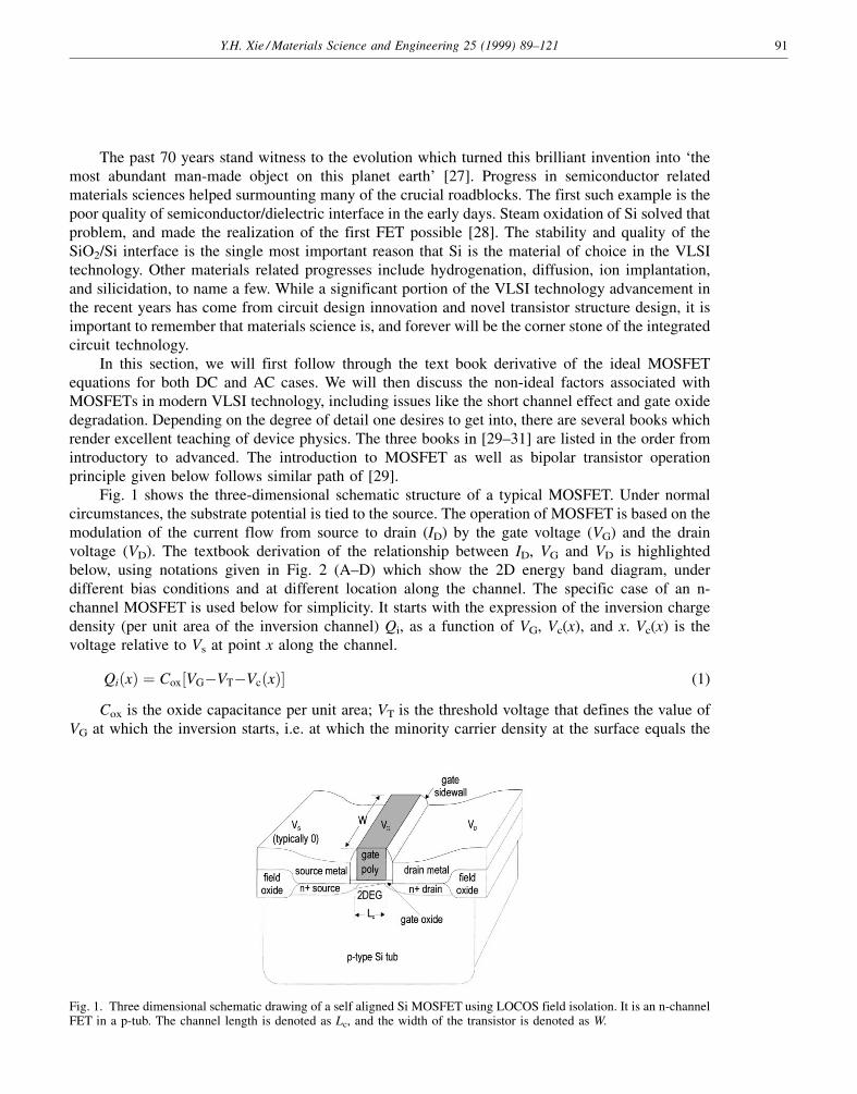
Fig. 1 shows the three-dimensional schematic structure of a typical MOSFET. Under normalcircumstances, the substrate potential is tied to the source. The operation of MOSFET is based on themodulation of the current flow from source to drain (ID) by the gate voltage (VG) and the drainvoltage (VD). The textbook derivation of the relationship between ID, VG and VD is highlightedbelow, using notations given in Fig. 2 (A±D) which show the 2D energy band diagram, underdifferent bias conditions and at different location along the channel. The specific case of an n-channel MOSFET is used below for simplicity. It starts with the expression of the inversion chargedensity (per unit area of the inversion channel) Qi, as a function of VG, Vc(x), and x. Vc(x) is thevoltage relative to Vs at point x along the channel.
Qi�x� � Cox�VGÿVTÿVc�x�� (1)
Cox is the oxide capacitance per unit area; VT is the threshold voltage that defines the value ofVG at which the inversion starts, i.e. at which the minority carrier density at the surface equals the
Fig. 1. Three dimensional schematic drawing of a self aligned Si MOSFET using LOCOS field isolation. It is an n-channelFET in a p-tub. The channel length is denoted as Lc, and the width of the transistor is denoted as W.
Y.H. Xie / Materials Science and Engineering 25 (1999) 89±121 91

majority carrier density in the bulk.
VT � VFB � 2B ��������������������������2"sqN 2B� �p
Cox
(2)
In Eq. (2), VFB is known as the flat band voltage, which is the VG necessary to bring the energyband at location x to the situation described in Fig. 2 (B). The difference between the work functionof the gate and the bulk semiconductor under the gate, and the presence of interface states, cause theVFB to be non-zero. The second term, 2B, is the condition under which the electron density at thesurface equals the hole density in the bulk, i.e. the onset of inversion. The third term represents theportion of VG needed to form the depletion layer. After the onset of inversion, the depletion layerwidth becomes nearly constant, i.e. independent of VG.
Fig. 2. Schematics and 2D energy band diagrams of an n-channel MOSFET under various bias conditions. (A) a schematicof the NMOSFET structure; (B) 2D band diagram under zero bias and without interface or oxide charge; (C) 2D handdiagram under positive gate bias; and (D) 2D band diagram under positive gate as well as drain bias. (after [102]).
92 Y.H. Xie / Materials Science and Engineering 25 (1999) 89±121
Using Eq. (1), the expression for the current flowing the inversion channel can be written interms of Qi and Vc at any point x along the channel according to Ohm's law:
ID � W�QiEx � W�Cox�VGÿVTÿVc�x�� dVc�x�dx
(3)
Since Vc(0) = 0 (following convention) and Vc(Lc) = VD are known, integrating ID from 0 to Lc
gives the relationship between ID, VG and VD:
ID � �CoxW
Lc
�VGÿVT�VDÿV2D
2
� �(4)
Eq. (4) is the basic DC equation for MOSFET operation. The entire derivation is carried outunder the gradual channel approximation which requires the longitudinal electric field component (inthe direction parallel to the channel) is much less than the transverse component. This is not to beconfused with the long channel approximation in which the channel length, Lc, is much longer thanthe depletion widths at the source and drain. While MOSFET miniaturization pushes constantlyagainst the long channel approximation, the gradual channel approximation is generally valid.
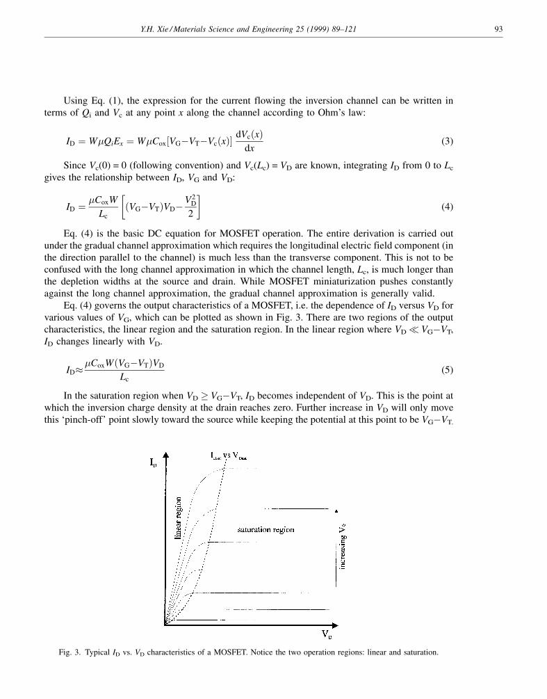
Eq. (4) governs the output characteristics of a MOSFET, i.e. the dependence of ID versus VD forvarious values of VG, which can be plotted as shown in Fig. 3. There are two regions of the outputcharacteristics, the linear region and the saturation region. In the linear region where VD� VGÿVT,ID changes linearly with VD.
ID��CoxW�VGÿVT�VD
Lc
(5)
In the saturation region when VD � VGÿVT, ID becomes independent of VD. This is the point atwhich the inversion charge density at the drain reaches zero. Further increase in VD will only movethis `pinch-off' point slowly toward the source while keeping the potential at this point to be VGÿVT.
Fig. 3. Typical ID vs. VD characteristics of a MOSFET. Notice the two operation regions: linear and saturation.
Y.H. Xie / Materials Science and Engineering 25 (1999) 89±121 93
In other words, ID now becomes dependent on Lc which is a very slow varying function of VD.
ID��CoxW
2Lc
�VGÿVT�2 (6)
MOSFETs are typically biased in the saturation region for both analog and digital applications.From Eq. (4), several parameters that are of generic importance of MOSFET performance can bederived. The first of which is the degree of control VG has on ID for VG > VT, known as thetransconductance, gm. In the linear region,
gm � dID
dVG
� �CoxWVD
Lc
(7)
Notice that gm in this case is dependent on VD, but is independent of VG. In the saturation region,
gm � dID
dVG
� �CoxW VGÿVT� �Lc
(8)
gm is independent of VD. In fact, as VD increases beyond the saturation point, Lc decreases slightlywith VD, and so does gm. In the case when VG < VT and VD� 0, the quantity corresponding to gm isknown as the subthreshold swing, S. S is defined as the amount of change in VG which results in thechange of ID by one decade.
S� kT
q�ln10� 1� Cd
Cox
� �(9)
Cd is the depletion layer capacitance. S describes how abruptly a MOSFET can be switched on or off,and is of paramount importance in low power applications.
Aside from the dependence on VD, gm also depends on the operation frequency. This is becausea minimum amount of time is needed for a MOSFET to be switched on or off. The electrons in thechannel have to have the time to move from the source to the drain. gm starts to degrade as theoperating frequency approaches this limit. The cutoff frequency, fT, is defined as the frequency atwhich an equivalent circuit gives unity current gain.
fT � gm
2��WLcCox � Cp� (10)
Cp is the parasitic capacitance. For Cp� Cox, fT is proportional to gm/Cox.The progress in VLSI technology brought about the continued shrinking of MOSFET
dimensions, also known as scaling. The well known Moore's curve shows that the channel length hasbeen shrinking by about 13% per year for the past 35 years [32]. As channel lengths are reduced tobelow certain value, the long channel approximation used in deriving MOSFET characteristics is nolonger valid. This deviation from the `ideal' characteristics is categorically known as short channeleffects. Such deviation complicates device operation and is highly undesirable. Three major shortchannel effects are described below.
The first short channel effect influences the saturation current. During the process of scaling, thesupply voltage has not been scaled at an equivalent rate as the device dimension due to the fact thatchips have to work in systems which have standardized supply voltages that can not be changed withindividual chips. In addition, there are some fundamental factors affecting the minimum operating
94 Y.H. Xie / Materials Science and Engineering 25 (1999) 89±121

voltage: the thermal noise on the order of kT/q, and the finite subthreshold swing, S (59 mV/decminimum), which dictates a minimum voltage swing needed to switch a MOSFET from `off' to `on'.These restrictions result in a high longitudinal electric field in the channel region.
It is well known that the drift velocity of electron (and hole) varies with electric field in a linearfashion up to a certain value. Beyond that, the velocity becomes independent of the electric field, i.e.the drift velocity saturates [33]. The saturated velocity value, (vsat) is material dependent. In Si, thisvalue is about 1 � 107 cm/s, and the electric field value at which velocity saturates is about1 � 105 V/cm. A rough estimate indicates that for 0.5 mm channel length, a VD = 5 V will cause theaverage longitudinal field to reach the 1 � 105 V/cm value. Velocity saturation causes the MOSFETto enter into the saturation region earlier, before VD reaches VGÿVT. The value of the saturatedcurrent becomes:
ID � WCox�VGÿVT�vsat (11)
and the associated gm becomes:
gm � WCoxvsat (12)
Notice that in this case, ID becomes linearly dependent on VGÿVT since the longitudinal fielddependence is no longer there. As a result, gm becomes independent of VGÿVT.
The second short channel effect has to do with the dependence of VT on the effect channellength. In deriving the ideal MOSFET characteristics, the channel length is defined as the distancebetween the source and the drain. As the channel length becomes shorter and shorter, however, thisdefinition needs to be refined. The effective channel length, Leff, is actually the length of the channelsegment within which electric field lines from mobile carriers terminate on, or originate from, thegate. This length is the physical length between the source and the drain, Lc, minus the depletionwidths at the source and the drain. Under drain bias, these depletion widths could become asignificant fraction of Lc. In other words, the effective channel length of a short channel MOSFEThas a non-negligible dependence on VD. This dependence has these consequences: ID is dependent onVD in both the subthreshold region and the saturation region, because of the decrease of Leff withincreasing VD. The threshold voltage, VT, decreases with VD via a reduction in the amount of chargethe gate controls with increasing VD.
The third short channel effect is from more or less the same origin as the second. A change inVD alters the amount of charge under the gate significantly when the channel length becomes shorter,resulting in a change in the threshold voltage, VT. In other words, VT becomes dependent on VD.Consequently, ID in both the subthreshold and saturation regions has an increased dependence on VD.
3. Introduction to bipolar junction transistors (BJTs)
The BJT operation theory formulated by Shockley in 1947 [34] has been used as the basis forthe current understanding of this transistor family. BJT is the second most used transistor in the VLSIindustry, next to the MOSFET. A brief discussion about its characteristics should help theunderstanding of the advantages and the limitations of MOSFETs. Since the objective of this articleis MOSFETs, the discussions on BJTs will be limited to an introductory level.
Fig. 4 (A) shows the cross-section view of a typical BJT. It is composed of two pn junctiondiodes connected back-to-back with one very important feature: the pn junctions are in very closeproximity of each other. The definition of close is measured by the minority carrier diffusion length,
Y.H. Xie / Materials Science and Engineering 25 (1999) 89±121 95
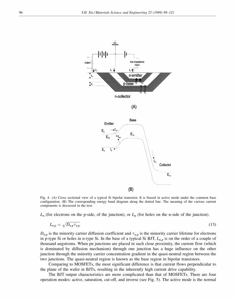
Ln (for electrons on the p-side, of the junction), or Lp (for holes on the n-side of the junction).
Ln;p ����������������Dn;p�n;p
p(13)
Dn,p is the minority carrier diffusion coefficient and �n,p is the minority carrier lifetime for electronsin p-type Si or holes in n-type Si. In the base of a typical Si BJT, Ln,p is on the order of a couple ofthousand angstroms. When pn junctions are placed in such close proximity, the current flow (whichis dominated by diffusion mechanism) through one junction has a huge influence on the otherjunction through the minority carrier concentration gradient in the quasi-neutral region between thetwo junctions. The quasi-neutral region is known as the base region in bipolar transistors.
Comparing to MOSFETs, the most significant difference is that current flows perpendicular tothe plane of the wafer in BJTs, resulting in the inherently high current drive capability.
The BJT output characteristics are more complicated than that of MOSFETs. There are fouroperation modes: active, saturation, cut-off, and inverse (see Fig. 5). The active mode is the normal
Fig. 4. (A) Cross sectional view of a typical Si bipolar transistor. It is biased in active mode under the common baseconfiguration. (B) The corresponding energy band diagram along the dotted line. The meaning of the various currentcomponents is discussed in the text.
96 Y.H. Xie / Materials Science and Engineering 25 (1999) 89±121
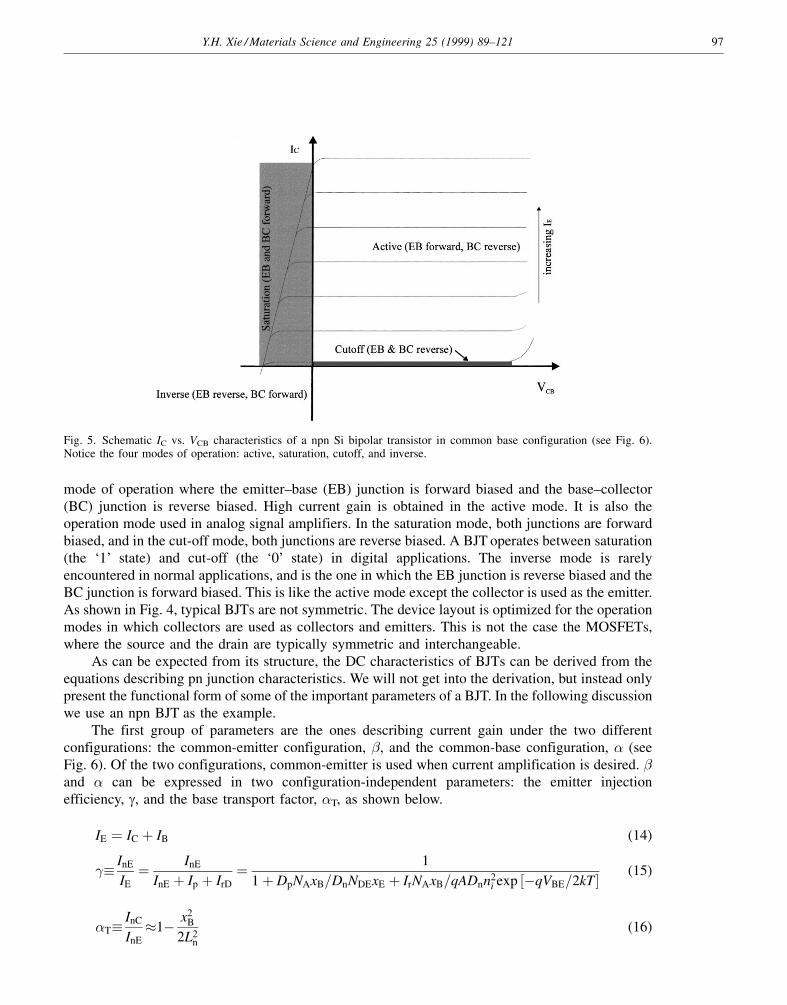
mode of operation where the emitter±base (EB) junction is forward biased and the base±collector(BC) junction is reverse biased. High current gain is obtained in the active mode. It is also theoperation mode used in analog signal amplifiers. In the saturation mode, both junctions are forwardbiased, and in the cut-off mode, both junctions are reverse biased. A BJT operates between saturation(the `1' state) and cut-off (the `0' state) in digital applications. The inverse mode is rarelyencountered in normal applications, and is the one in which the EB junction is reverse biased and theBC junction is forward biased. This is like the active mode except the collector is used as the emitter.As shown in Fig. 4, typical BJTs are not symmetric. The device layout is optimized for the operationmodes in which collectors are used as collectors and emitters. This is not the case the MOSFETs,where the source and the drain are typically symmetric and interchangeable.
As can be expected from its structure, the DC characteristics of BJTs can be derived from theequations describing pn junction characteristics. We will not get into the derivation, but instead onlypresent the functional form of some of the important parameters of a BJT. In the following discussionwe use an npn BJT as the example.
The first group of parameters are the ones describing current gain under the two differentconfigurations: the common-emitter configuration, �, and the common-base configuration, � (seeFig. 6). Of the two configurations, common-emitter is used when current amplification is desired. �and � can be expressed in two configuration-independent parameters: the emitter injectionefficiency, g, and the base transport factor, �T, as shown below.
IE � IC � IB (14)
� InE
IE
� InE
InE � Ip � IrD
� 1
1� DpNAxB=DnNDExE � IrNAxB=qADnn2i exp �ÿqVBE=2kT � (15)
�T� InC
InE
�1ÿ x2B
2L2n
(16)
Fig. 5. Schematic IC vs. VCB characteristics of a npn Si bipolar transistor in common base configuration (see Fig. 6).Notice the four modes of operation: active, saturation, cutoff, and inverse.
Y.H. Xie / Materials Science and Engineering 25 (1999) 89±121 97
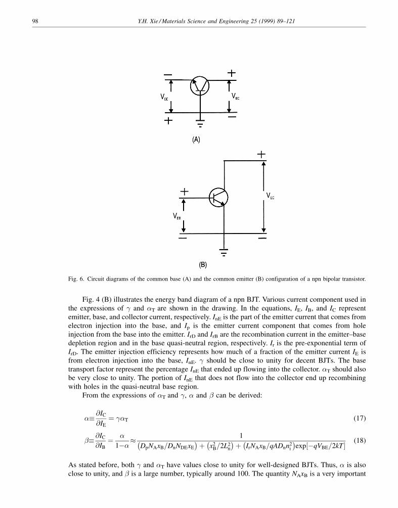
Fig. 4 (B) illustrates the energy band diagram of a npn BJT. Various current component used inthe expressions of and �T are shown in the drawing. In the equations, IE, IB, and IC representemitter, base, and collector current, respectively. InE is the part of the emitter current that comes fromelectron injection into the base, and Ip is the emitter current component that comes from holeinjection from the base into the emitter. IrD and IrB are the recombination current in the emitter±basedepletion region and in the base quasi-neutral region, respectively. Ir is the pre-exponential term ofIrD. The emitter injection efficiency represents how much of a fraction of the emitter current IE isfrom electron injection into the base, InE. should be close to unity for decent BJTs. The basetransport factor represent the percentage InE that ended up flowing into the collector. �T should alsobe very close to unity. The portion of InE that does not flow into the collector end up recombiningwith holes in the quasi-neutral base region.
From the expressions of �T and , � and � can be derived:
�� @IC
@IE
� �T (17)
�� @IC
@IB
� �
1ÿ��1
DpNAxB=DnNDExE
ÿ �� x2B=2L2
n
ÿ �� IrNAxB=qADnn2i
ÿ �exp�ÿqVBE=2kT � (18)
As stated before, both and �T have values close to unity for well-designed BJTs. Thus, � is alsoclose to unity, and � is a large number, typically around 100. The quantity NAxB is a very important
Fig. 6. Circuit diagrams of the common base (A) and the common emitter (B) configuration of a npn bipolar transistor.
98 Y.H. Xie / Materials Science and Engineering 25 (1999) 89±121

quantity in BJT design, and is known as the Gummel number. It is the sheet density of holes in thequasi-neutral base region, and is more generally expressed as:
GN�ZxB
0
NAdx (19)
As is obvious from Eq. (18), the smaller the GN, the larger the common-emitter gain, �. Thelower limit of GN is imposed by the punch-through condition, where the width of the quasi-neutralbase region reaches zero and the transistor action is lost. Too small a GN also causes increased basereistance, thus limiting the high frequency performance of the BJT. For a given GN, one would like tohave as thin a base region as possible in order to reduce the base width means increasing the basedoping concentration, eventually the emitter±base junction will become significant. Tunnelingcurrent reduces , and thus �, the BJT current gain. For a Si BJT, this occurs at a base dopingconcentration of about 3 � 1018 mÿ3. For a heterojunction BJT (commonly known as HBT),however, the base doping concentration can be made much higher by reducing the emitter dopingconcentration to suppress the tunneling current. This will allow the use of a thin base with low baseresistance. This is the most significant advantage of a SiGe/Si HBT [35] versus a homojunction BJT.
There are two other important effects to keep in mind during BJT design: Early effect and Kirkeffect. Early effect comes from the narrowing of the quasi-neutral base region as a result ofincreasing base±collector reverse bias voltage. It results in the non-saturation of the collector±emittervoltage, VCE. The voltage at which the extrapolation of the family of I±V curves converge at I = 0 isknown as early voltage, VA.
VA� qNAL2B
"s
(20)
It is desirable to have as large an early voltage as possible, and 15 V is beginning to be consideredacceptable for certain applications. Higher base doping concentration lessens the early effect.Consequently, SiGe HBTs typically have much higher early voltage compared with Si BJTs [36].Kirk effect is because of high current injection when the space charge of the injected mobile carrieris comparable to the space charge of the dopants on the collector side (the lower doped side) of thebase±collector junction [37]. The result is an increase in the effective base width, and is known asbase push-out. Kirk effect limits the maximum current flowing through a BJT. While a highercollector doping concentration reduces Kirk effect, it also reduces the breakdown voltage, VCBO andVCEO. A trade-off based on specific application is again necessary.
VCEO � VCBO�1ÿ��1=n�VCBO
�1=n(21)
The transconductance of a BJT can be written as following:
gm� @IC
@VBE
����VCE
� qIC
kT(22)
For BJTs, large IC values result in high transconductance.The cut-off frequency, fT, is customarily used to show the intrinsic speed of a transistor. In BJTs,
fT is defined as the frequency at which the common-emitter short circuit current gain is unity. It can
Y.H. Xie / Materials Science and Engineering 25 (1999) 89±121 99
be visualized as four delay elements in series:
1
2�fT� �E � �B � �dC � �C � �T CE � CC� �
IE
� L2B
2Dn
� WdC
2vsat
� RCCC (23)
�B and �dC represents the transit time in the quasi-neutral base region and the base±collectordepletion region, respectively. �E is the emitter charging time, and �C is the collector charging time.In Eq. (23), the two elements associated with charging time have the form of resistance±capacitanceproducts, whereas the elements associated with transit time have the form of distance over time.Another frequently used parameter related to the transistor speed is the maximum oscillationfrequency, fmax
fmax� 1
2S
fT
2�rBCBC
� �1=2
(24)
S is the emitter strip width, rB is the base resistance, and CBC is the base±collector capacitance. fmax
is more of an overall figure of merit comparing to fT in that certain parasitic elements are taken intoconsideration.
4. Typical applications of MOSFET and BJT
When assessing the relative advantages and disadvantages of various alternatives to the SiMOSFET and BJT, it is very important to keep in mind that the winning edge of Si VLSI is its costeffectiveness and manufacturability. Any viable alternatives or improvements to the technology mustpreserve these characteristics. There are many transistor structures, notably various types ofcompound semiconductor transistors, that can perform better that the Si counterpart in terms of gm
and fT. The cost effectiveness and manufacturability concerns confine these devices to nicheapplications. To help appreciate this point further, it is useful to mention that the largest obstaclewhich impedes combining BJTs with CMOS, commonly known as the BiCMOS technology, is thecost issue. Without the cost concern, many of the technological challenge people face today wouldnot be present.
The major advantages of CMOS technology include ease of fabrication, the availablecomplementary devices (NMOSFET and PMOSFET), a truly capacitive gate that can be over driven,and with inherently better linearity. The structural simplicity of MOSFETs comparing to othertransistor structures is the underlying reason for the high yield and the low cost. The availability ofcomplementary devices provides circuit design flexibility, and allows circuits to have near zeroquiescent power consumption. The capacitive gate permits transistors to draw zero current in an `on'state. It can also withstand zero to full supply voltage swing at the input which is a circuit designflexibility in digital applications. The linearity comes from Eq. (12), where gm is independent of IDS
or VDS. The implication of higher linearity is am improved bit error rate. In addition, the VT ofMOSFETs can be adjusted almost at will, in contrast to BJTs, in which the turn on voltage is dictatedby the built-in voltage of a Si pn junction. This will ultimately allow MOSFETs to operate in circuitswith lower voltage, and thus lower power consumption. As a result, CMOS is most widely used indigital applications such as memories and logic circuits.
The major challenges confronting the front end of the CMOS technology (the transistorstructure excluding metal interconnects) today include device miniaturization, which requires
100 Y.H. Xie / Materials Science and Engineering 25 (1999) 89±121
improved lithographic tools and control of dopant profile, suppressing short channel effects aschannel length shrinks continuously, and gate oxide reliability.
BJTs, on the other hand, have inherently higher gm as mentioned before. Furthermore, the ratioof gm/ID, an important figure of merit in analog circuit design, is always larger for BJTs compared toCMOS. The difference is at least two times for the entire range of practical MOSFET channel widthto length ratios, and could be as large as several orders of magnitude [38]. Consequently, BJTsalways have much higher gain compared to the MOSFET counterpart. The higher gain together withthe existence of a more experienced bipolar RF design community render BJTs the device of choicefor analog applications. However, CMOS based RF circuits have emerged recently [39], and arepoised to claim their rightful place in the rapidly developing RF market.
5. MOSFET performance analysis
In this section, several crucial parameters in MOSFET performance are analyzed in detail,together with the various factors influencing them. These parameters are: transconductance, gm;switching speed, fT, power consumption, and transistor packing density. While they will be treatedindividually in the following discussion, it is important to realize that they are all inter-related in oneway or another. The task of optimizing a transistor design is a game of trade-offs.
5.1. Transconductance
To appreciate the advantages of dealing with strain, it is appropriate at this point to review thecurrent understanding of the factors affecting transconductance in unstrained Si channel MOSFETs.The reason for focusing on transconductance in that almost all the expected advantages of usingstrained layers are related to transconductance. The discussion is divided into three regimes: low andhigh longitudinal electric field, and with very short channels under high longitudinal electric field.
5.1.1. Under low longitudinal electric field
Under low longitudinal field, the effective channel mobility (�eff) is proportional to thetransconductance. The effective channel mobility follows a universal curve (in a plot of the effectivechannel mobility versus the effective transverse electric field Eeff) which is independent of thechannel doping concentration up to 1017 cmÿ3 [40]. �eff and Eeff are defined as follows:
�eff �LgD
WqNs
(25)
Eeff � q�NB � �Ns�"s
(26)
�eff is a representation of the average carrier drift mobility in the channel region. Eeff is the transverseelectric field experienced by the carriers in the channel averaged over the carrier population. Theuniversal curve of electrons has two distinct slopes at 300 K. In cases when Eeff is below 0.5 mV/cm,�eff is proportional to Eeff
ÿ0.3 which is believed to be the signature of acoustic phonon scattering. For Eeff
above 0.5 mV/cm, the proportionality approaches Eeffÿ0.3. Interface roughness is believed to be the
limiting scattering mechanism in this case, as the high Eeff draws the electron population closer to theSiO2/Si interface. At low temperatures, the phonon population decreases with temperature, leavinginterface roughness scattering to be the dominant scattering mechanism throughout the range of Eeff.
Y.H. Xie / Materials Science and Engineering 25 (1999) 89±121 101

The universal curve for holes does not have such distinct regions. It has been shown that at300 K, the curve is a mixture of the interface roughness scattering (Eeff
ÿ1) and the acoustic phononscattering (Eeff
ÿ0.3). At lower temperatures and high Eeff, the curve converges toward the interfaceroughness limited regime.
The common feature between electrons and holes is that interface roughness and acousticphonon are the dominant scattering mechanisms to consider at 300 K for channel dopingconcentration levels up to 1017 cmÿ3. Coulomb scattering increasingly important as NB gets above1018 cmÿ3 [41], as in deep submicron technologies.
5.1.2. Under high longitudinal electric fieldUnder high longitudinal electric field, electron velocity saturation becomes important in the
transport picture. Because the longitudinal electric field is not uniform across the channel, the onsetof velocity saturation manifests as a reduced dependence of the effective channel velocity on thelongitudinal field. In other words, there is always a portion of the channel near the source withinwhich the electron velocity is below vsat, with the actual velocity dependent on the carrier mobility.Over the rest of the channel, mobility has no direct impact on the carrier velocity.
It is also interesting to notice that the average carrier velocity measured in a MOSFET channeltype of structure does not saturate at the value of 1 � 107 cm/s, as can be seen from Fig. 7 [42].When the effect of the source±drain series resistance is properly corrected, the average carriervelocity for <0.1 mm channel length does go beyond 1 � 107 cm/s (Fig. 7), indicative of velocityovershoot [43]. It should be pointed out that specially engineered FET structures such as the one in[44] are needed in order to ensure a relatively constant longitudinal electric field in the channelregion, and thus a meaningful average velocity.
Due to their lower mobility, holes enter into the velocity saturation regime at a much higherlongitudinal electric field. For 0.3 mm CMOS using 3.3 V power supplies, PMOSFETs are still in the
Fig. 7. Plot of the average channel velocity in Si MOSFETs vs. the effective channel length. It is obvious that the velocitydoes not saturate even though the longitudinal electric field is higher than 105 V/cm [42].
102 Y.H. Xie / Materials Science and Engineering 25 (1999) 89±121

regime in which carrier mobility dominates the velocity-field relationship, i.e. ID in the saturationregion in roughly proportional to (VGÿVT)2 as in Eq. (6). Since the transconductance is related to theeffective channel velocity, a higher hole mobility will result in a higher PMOSFETtransconductance. In contrast, higher electron mobility will have much less effect on the NMOSFETtransconductance because of velocity saturation.
5.1.3. Very short channels with high longitudinal electric field
As channel lengths shrink into the deep submicron regime, velocity overshoot [44] becomes animportant influence on the effective channel velocity. It has been established that carrier velocityovershoots the saturation velocity value within one energy relaxation time. Therefore, velocityovershoot becomes important when the carrier transient time across the channel region is comparableto the energy relaxation time. This happens when the channel length approaches 0.1 mm, and thetransient time approaches 1 ps. A carrier in the channel comes across a region of low field near thesource, a region with saturated velocity near the center of the channel, and a region of velocityovershoot near the drain, as has been shown by simulation [45±47]. Experimental results usingsilicon-on-insulator (SOI) MOSFET structure with �0.1 mm channel lengths support the simulationresult [48]. The significance of the SOI structure is that it allowed the gradual channel approximationto be maintained down to very short channel lengths.
As the contribution of velocity overshoot to the effective channel velocity depends on theenergy relaxation time, altering the energy band structure should have a significant impact on theeffective channel velocity. It will become clear that one of the potential advantages of using strainedchannels is to alter the energy band structure in the channel region.
One last point to keep in mind before leaving this section is that under high transverse electricfield, Eeff, the energy quantization becomes non-negligible within the channel. This quantizationcould affect the energy relaxation process, whereby influence profoundly the degree of velocityovershoot.
5.2. Speed
While the predominant CMOS applications are in digital domain, i.e. memory gates and logicinverters, there begins to be more analog applications based on CMOS as well. Therefore, the subjectof speed is broken down into large signal switching and small signal applications. Only operation inthe saturation region will be considered since both digital and analog applications bias transistors inthis region. Situations with and without velocity saturation will be discussed separately.
5.2.1. Large signal switching
The large signal switching time consists the internal transit time for carriers to traverse thetransistor channel, tT, and the capacitor (load and parasitic) charging and discharging time in theform of RC delay, tRC.
It can be shown that for the velocity saturated case, tT has the form:
tT/ Le
vsat
/WCoxLe
gm
(27)
The expression becomes
tT/ L2e
��VGÿVT�/WCoxLe
gm
(28)
Y.H. Xie / Materials Science and Engineering 25 (1999) 89±121 103

in the absence of velocity saturation. As expected, tTs in both cases are approximately proportionalto the channel length divided by the velocity. It is also helpful to notice that tTs are inverselyproportional to gm in both cases.
The time constant, tRC, for charging and discharging of external capacitance can be shown tohave the following form:
tRC/CL
gm
(29)
CL represents the total load and parasitic capacitance. The proportional constant varies from around3 to around 20, and is smaller for discharging process. A higher gm means higher current drive, or ashorter RC charging time.
The total delay of a circuit element depends on the combination of tT and tRC. Since both timeconstants are inversely proportional to gm, a high gm results directly in the improvement of the circuitspeed.
5.2.2. Small signal characteristicsThe cutoff frequency, fT, is shown in Eq. (10). It is proportional to the ratio of gm/(Cox + Cp).
Under circumstances when Cp�Cox higher gm results directly in higher fT. The most straightforwardway of increasing gm is to have a thinner gate oxide. This approach will have a diminishing impacton fT if Cox is equal or larger than Cp. On the other hand, fT will always be proportional to gm if gm
can be increased while keeping Cox constant.
5.3. Power consumption
The parameter that is often used when considering power consumption is the power±delayproduct. It is important because the product represents a fundamental trade-off once the materialsystem, in this case Si and SiO2, is given. Reducing power consumption almost necessarily result incompromising the speed performance. This quantity has increased importance in an era whenportable electronics gain popularity, and as the density of power dissipation goes up with increasingpacking density. It is the objective in transistor design to meet the power or speed requirement whileminimizing the power±delay product.
The power±delay product has the following form:
powerÿdelay� 2
3CoxLZ VGÿVT� �2 (30)
The product is proportional to the total gate capacitance, and quadratic to the gate voltage, VGÿVT.As will be shown below, an alternative material system such as SiGe/Si offers the possibility of
reducing the power±delay product as compared to the conventional Si/SiO2 structures.
5.4. Packing density
For a given gate length, the gate width is determined by the required current drive, or gm.Generally speaking, any improvement in gm will result in a proportional reduction in transistor sizes,or alternatively, a proportional increase in the packing density. In CMOS circuits with N- andPMOSFETs having the same channel length as defined by the lithographic capability of a specifictechnology, PMOSFETs are the ones that have lower gm. Thus, PMOSFETs typically have larger
104 Y.H. Xie / Materials Science and Engineering 25 (1999) 89±121
width so that N- and P-transistors could have comparable current drive capability. The consequenceis that PMOSFETs occupy majority of the Si real estate. The packing density of a CMOS circuit canbe greatly improved if hole mobility in the PMOSFET channel can be increased.
6. Why SiGe: the perceived advantages scrutinized
In this section, we present the perceived advantages of using SiGe for improving the crucialFET performance parameters. These perceived advantages are scrutinized in light of the currentregime of Si CMOS operation.
6.1. The only high quality heterointerface on Si
Unlike GaAs and other III±IV compound materials, Si does not have other cubic semiconductormaterials lattice matches to it. This is the reason why Si trails compound semiconductors in terms ofthe various heterojunction devices. Ge is the only elemental semiconductor with the closest latticeconstant to that of Si. In other words, SiGe/Si is the only crystalline±crystalline interface on Si thatcan potentially be as high quality as those in III±V semiconductors. The lattice mismatch is about4% (with aSi = 5.43095 AÊ , aGe = 5.64613 AÊ ). While 4% does not seem to be a large number, it isexceedingly large from the epitaxial growth point of view. This point can be appreciated by lookingat the following two materials issues: strain relaxation via dislocation, and epitaxial growth in 3Dgrowth mode.
The onset of strain relaxation via dislocation is dictated by the equilibrium critical layerthickness [49], tc. tc decreases with increasing strain, and is about 12 AÊ for Ge on Si with the 4%strain. This is the maximum Ge layer thickness one can epitaxially grow on a Si substrate before theentire structure becomes energetically favorable for dislocation introduction. This means while onemight be able to epitaxially grow Ge layers thicker than 12 AÊ on Si substrates with minimaldislocation density by controlling the growth temperature and rate, dislocation will set in if the filmis subjected to thermal cycles, i.e. the film is thermodynamically unstable. Obviously, 12 AÊ is anumber that is too small to be useful for most device applications.
In addition to dislocation, there is more complication when epitaxial growth of Ge in Si isattempted. A film with such high strain tends to grow in three dimensional islanding mode [50]rather than 2D, layer-by-mode. This is due to the lowering of surface step energies when the film isunder such high compressive strain [51,52], as aGe is 4% larger than aSi. The result is a film withsurface undulations of �100 AÊ amplitude and �1000 AÊ period. Such non-flat surface makes itdifficult to use the film for device applications.
If Ge/Si heterostructure is the only option we have, device applications would have been out ofthe question. What enabled the entire field of SiGe/Si research is the complete miscibility of Ge andSi [53]. In other words, SiGe alloy with any percentage of Ge forms random solid solution with nosignificant phase segregation of any sort. The lattice constant of SiGe can thus be varied in acontinuous fashion from that of Si to that of Ge. With lattice mismatch of less 1%, whichcorresponds to Si1ÿx Gex with x < 0.25, high quality SiGe films of up to �100 AÊ thickness can beepitaxially grown on Si substrates with ease. The resulting heterostructure can also bethermodynamically stable. The heterointerface between SiGe and Si can be made with high quality,both from the minority carrier lifetime [22,23] as well as the majority carrier transport [17] points ofview. Such properties of the materials systems render it the only high quality heterointerface on thetechnologically important Si (100) substrate, and made it possible for realistic device applications.
Y.H. Xie / Materials Science and Engineering 25 (1999) 89±121 105
6.2. Transconductance improvement due to strain
The strain present in a SiGe/Si heterostructure modifies the energy band structure, resulting inchanges in the energy band gap value, the curvature at the conduction and valence band minima, andthe degeneracy. As will be shown, changes in the curvature affect the carrier effective mass, andchanges in the degeneracy affect both carrier effective masses, mobility, and effective channelvelocity. While the change in the energy band gap is used in the heterojunction bipolar transistors toimprove the performance, the change in carrier effective masses, channel mobilities and effectivechannel velocities are the reasons for using the strained Si, Ge, or SiGe for FET applications.
All the expected improvement to a MOSFET using a strained channel is in transconductance.Depends on the channel lengths, the improvement come either from the channel mobility, or theeffective channel velocity.
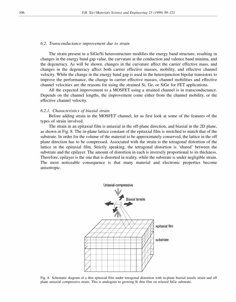
6.2.1. Characteristics of biaxial strain
Before adding strain in the MOSFET channel, let us first look at some of the features of thetypes of strain involved.
The strain in an epitaxial film is uniaxial in the off-plane direction, and biaxial in the 2D plane,as shown in Fig. 8. The in-plane lattice constant of the epitaxial film is stretched to match that of thesubstrate. In order for the volume of the material to be approximately conserved, the lattice in the offplane direction has to be compressed. Associated with the strain is the tetragonal distortion of thelattice in the epitaxial film. Strictly speaking, the tetragonal distortion is `shared' between thesubstrate and the epilayer. The amount of distortion in each is inversely proportional to its thickness.Therefore, epilayer is the one that is distorted in reality, while the substrate is under negligible strain.The most noticeable consequence is that many material and electronic properties becomeanisotropic.
Fig. 8. Schematic diagram of a thin epitaxial film under tetragonal distortion with in-plane biaxial tensile strain and offplane uniaxial compressive strain. This is analogous to growing Si thin film on relaxed SiGe substrate.
106 Y.H. Xie / Materials Science and Engineering 25 (1999) 89±121
From the electronic transport point of view, strain changes the energy band minima for both thevalence as well as the conduction band. The amount of the relative change depends on whether it isthe valence or the conduction band, whether the 2D channel is in Si, Ge, or SiGe, and whether thechannel is under tensile or compressive strain. Energy band discontinuities for various combinationof strain in different layers can be calculated theoretically, as detailed by Van de Walle and Martin[12]. Electrons are confined in a strained Si layer while holes are confined in a strained Ge layergrown on relaxed SiGe.
6.2.2. Carrier mobility in strained channels
Carrier mobility improvements using a strained channel come mainly from two sources: areduction of the in-plane carrier effective mass, and a reduction of interval scattering.
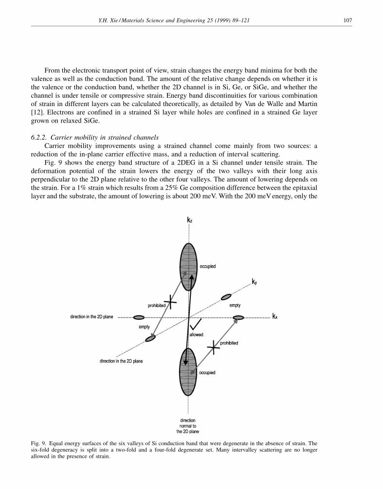
Fig. 9 shows the energy band structure of a 2DEG in a Si channel under tensile strain. Thedeformation potential of the strain lowers the energy of the two valleys with their long axisperpendicular to the 2D plane relative to the other four valleys. The amount of lowering depends onthe strain. For a 1% strain which results from a 25% Ge composition difference between the epitaxiallayer and the substrate, the amount of lowering is about 200 meV. With the 200 meV energy, only the
Fig. 9. Equal energy surfaces of the six valleys of Si conduction band that were degenerate in the absence of strain. Thesix-fold degeneracy is split into a two-fold and a four-fold degenerate set. Many intervalley scattering are no longerallowed in the presence of strain.
Y.H. Xie / Materials Science and Engineering 25 (1999) 89±121 107
two-fold degenerate valleys are occupied at room temperature. Therefore, the longitudinal effectivemass determines the quantization energy in a strained Si quantum well, whereas the transverseeffective mass determines the electron motion along the 2D plane, such as in the channel of aMOSFET. The anisotropy comes directly from the anisotropic nature of the biaxial strain. The strainlowers the effective mass of the 2DEG from 0.33 to 0.19 m0 in the 2D plane.
Abstreiter and coworkers first demonstrated 2DEGs with reduced effective mass in a strained Silayer in 1985 [18]. The mobility value was not high due to the high dislocation density. Whencompositionally graded SiGe buffer was first introduced in 1991 (with which the threadingdislocation density was reduced by more than two orders of magnitude), the low temperature 2DEGmobility record was brought from less than 30 000 to 125 000 cm2/V s [19]. The record has beenpushed up to new heights continuously using refined structures [20]. Room temperature 2DEGmobility of well over 2000 cm2/V s has been measured [54,55].
It should be mentioned here that although the quantization in an unstrained Si channel alsocause an energy separation between the two-fold and the four-fold valleys, the separation energy ismuch smaller than the one caused by strain. Only a slight preferential occupation by electrons existsin the unstrained case. In contrast, nearly 100% of electrons (for electron sheet densities up to mid1012 cmÿ2) are in the two-fold valleys at room temperature in Si channel under 1% tensile strain.
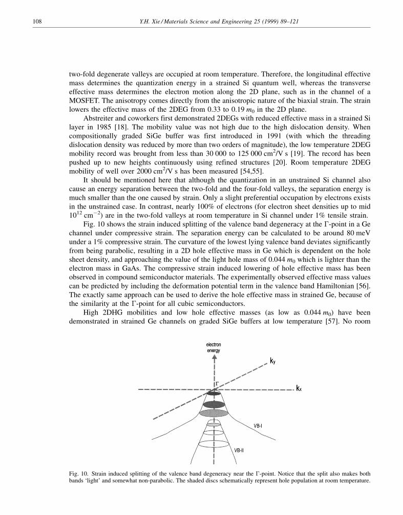
Fig. 10 shows the strain induced splitting of the valence band degeneracy at the ÿ-point in a Gechannel under compressive strain. The separation energy can be calculated to be around 80 meVunder a 1% compressive strain. The curvature of the lowest lying valence band deviates significantlyfrom being parabolic, resulting in a 2D hole effective mass in Ge which is dependent on the holesheet density, and approaching the value of the light hole mass of 0.044 m0 which is lighter than theelectron mass in GaAs. The compressive strain induced lowering of hole effective mass has beenobserved in compound semiconductor materials. The experimentally observed effective mass valuescan be predicted by including the deformation potential term in the valence band Hamiltonian [56].The exactly same approach can be used to derive the hole effective mass in strained Ge, because ofthe similarity at the ÿ-point for all cubic semiconductors.
High 2DHG mobilities and low hole effective masses (as low as 0.044 m0) have beendemonstrated in strained Ge channels on graded SiGe buffers at low temperature [57]. No room
Fig. 10. Strain induced splitting of the valence band degeneracy near the ÿ-point. Notice that the split also makes bothbands `light' and somewhat non-parabolic. The shaded discs schematically represent hole population at room temperature.
108 Y.H. Xie / Materials Science and Engineering 25 (1999) 89±121
temperature mobility data in such structures are available, due mainly to the difficulties ineliminating parallel channels in a modulation doped structure.
Strain lowers the effective mass for both 2DEG in tensile strained Si channel and 2DHG incompressively strained channels. The lowering of the effective masses results directly in improvedmobilities.
6.2.3. Intervalley scattering in strained channelIntervalley scattering limits both the carrier mobility and the amount of velocity overshoot.
Studies in this area are largely limited to theoretical calculations and computer simulations.Although approximate due to the potential oversight of some scattering mechanisms, these studiesprovide a clear physical picture of the transport process in strained channels.
From the mobility point of view, reducing intervalley scattering eliminates portion of thephonon spectrum that could otherwise interact with carriers. For example, the mobility limitingphonons with large k vectors in a Si channel under tensile strain are prevented from interacting with2DEGs because of the 200 meV energy gap between the two-fold and the four-fold degeneratevalleys [58]. Fig. 9 shows how the various intervalley scattering paths are eliminated by tensile strainfor 2DEGs. Similar reduction of intervalley scattering is expected for holes in strained channels,although it is more complicated to estimate the degree of the reduction.
The reduced intervalley scattering is expected to have a profound effect on the amount ofvelocity overshoot. It has been demonstrated using Monte Carlo simulation for 2DEGs in Si channelsunder tensile strain that both the momentum relaxation time and the energy relaxation time areincreased by up to four times [45,59] comparing to in unstrained Si channels. Consequently, electronvelocity near the drain could overshoot to three times the saturation velocity. The effective channelvelocity could increase to above the saturation velocity [45], as has been observed experimentally[42]. Similar analysis for 2DHGs is lacking.
Comparing to unstrained Si, it has been shown that for Si channels under tensile strain, theelectron mobility is higher by about 50% due to a lower effective mass and reduced intervalleyscattering. The amount of velocity overshoot is expected to be higher by as much as three times dueto the reduced intervalley scattering. Holes have higher mobility in Ge under compressive strain asthe effective mass is lowered by as much as a factor of five. In fact, similar reduction in holeeffective mass is expected for all cubic semiconductors under strain. However, it is interesting tonotice that none of the hole effective masses measured experimentally in compressively strainedSiGe channels on Si substrates show such reduction. There is no theoretical prediction about velocityovershoot for 2DHGs available.
6.3. VLSI circuit packing density
Any increase in transconductance can be used to increase circuit packing density. Highertransconductance allows for a narrower FET to deliver the same current drive under a given biasvoltage. This is true for both N- and P MOSFETs.
6.4. Perceived advantages scrutinized
Having reviewed all the potential advantages of using strained channels for MOSFETs, it ishelpful to take a closer look at which advantages are known facts, which are expected by theory, andwhich are simply wishful thinking.
Experimental as well as theoretical studies have established the following known facts: The in-plane 2DEG effective mass in Si channel under tensile strain is �0.2 m0. The separation energy
Y.H. Xie / Materials Science and Engineering 25 (1999) 89±121 109
between the two-fold and four-fold degenerate conduction band is about 200 meV under 1% strain,which decreases with strain. The room temperature 2DEG mobility can be well above 2000 cm2/V s.The in-plane 2DHG effective mass in Ge channel under compressive strain can be as low as�0.05 m0. And finally, the separation energy between the two valence bands at ÿ-point is about80 meV under 1% strain, which also decreases with strain.
Based on the theoretical understanding of the materials system, the following can be reasonablyexpected: The reduced intervalley scattering of 2DEG in strained Si will result in longer energyrelaxation time, making velocity overshoot a more significant element in transconductance. Thesame reduction will also contribute to a higher effective channel mobility. The decrease in the 2DHGeffective mass will result in an increase in the effective channel mobility.
The following subjects remain not understood: How do we properly model alloy scattering inSiGe/Si heterostructures, and what is the value of the interaction potential? What is the highestachievable 2DHG mobility improvement in a strained channel? How will the carrier densitydependence of the 2DHG effective mass impact the four characteristics of a MOSFET? Howwill the reduced 2DHG effective mass and the changed valence band structure affect the velocityovershoot? All these are in addition to the many materials and processing related issues that are notunderstood.
The potential of an increased velocity overshoot has been thought of as an advantage.Obviously, it is indeed an advantage in terms of transconductance. However, what hasn't beenbrought to people's attention is the potential problem associated with velocity overshoot. Namely,the increase in the kinetic energy of carriers at the drain junction could potentially increase the hotcarrier degradation of the gate oxide. Much of the Si VLSI research and development effort has beenfocusing on this exact issue in Si. Remedies such as lightly doped drain (LDD) and oxynitride areused to overcome the problem. It is certainly not an issue anybody can afford to ignore.
The discussion on the perceived advantages has been carried out using Si channels under tensilestrain for 2DEGs and Ge channels under compressive strain for 2DHGs. These are not the onlyheterostructures in which the above advantages can be realized. It is helpful to keep in mind thefundamental requirements for obtaining the improved transport properties, especially when readingthe next section in which various SiGe FET structures are discussed.
For 2DEGs, the channel resides in materials with Si-like conduction band structure (with sixconduction band minima along (1 0 0) directions), and the strain is tensile in the 2D plane and is onthe order of 1%. There is no reduction in electron effective mass in a Ge-like channel (with eightconduction band minima along (1 1 1) directions) due to symmetry. A compressively strained Si-likechannel will have an inplane effective mass close to the longitudinal effective mass of 0.98 m0 andnot much reduced intervalley scattering. In addition, the conduction band discontinuity between thestrained layer (channel) and the underlying layer must be such that electrons have lower or equalpotential energy in the channel. This will prevent the presence of a parallel channel in a MOSFET.From the materials point of view, a graded SiGe buffer layer is needed to apply tensile stress to Si.Graded SiGe buffers contain dislocations that may affect device performance or reliability. Thispoint will be discussed in more detail in Section 8.
For 2DHGs, the material can be any cubic semiconductor because of the similarity of theirvalence bands at ÿ-point, and the strain can be either tensile or compressive. In other words,improvement can be expected for compressively strained Ge, SiGe, or even Si under tensile strain.The only requirement is that 2DHGs have to have a preference to occupy the channel, similar to the2DEG case.
As will be seen in the next section, there are large variety of SiGe/Si FET structures. All of themmeet the fundamental requirements set forth in the preceding two paragraphs.
110 Y.H. Xie / Materials Science and Engineering 25 (1999) 89±121
7. Various SiGe FET structures
The discussion in this section is organized according to the material structure around thechannel region. The pros and cons of each structure in terms of electronic performance are discussed.Processing issues are postponed until the next section. Detailed results of experimentalmeasurements are intentionally de-emphasized because of the difficulty in carrying out meaningfulcomparison among various FET layouts, gate lengths, and processing details. Moreover,experimental devices usually do not have optimized structures, and device optimization is a subjectthat is beyond the scope of this article.
There are two common variation among all the FET categories to be discussed, namely,MODFET versus MOSFET, and mesa versus junction isolation. The advantage of the MODFETstructure is a lower thermal budged (no oxidation), and the disadvantage is the voltage drivelimitation (not allowing gate overdrive). Mesa isolation has the advantage of easily realizable in alaboratory environment, and the disadvantage of being non-planar, which is synonymous with poormanufacturability.
7.1. SiGe p-channel FETs
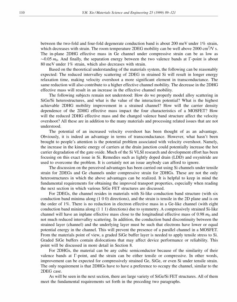
This class of devices represents the simplest structurally among the SiGe FET families.The earliest attempt can be traced back to 1986 [60], with numerous publications in the subsequentyears [61±67]. A typical structure includes a SiGe alloy layer (the channel) epitaxially grown ona Si substrate, followed by a Si cap layer. Portion of the Si cap layer is oxidized to form thegate dielectric. The rest of the transistor structure is pretty much the same as the Si counterpart.Fig. 11 shows a schematic drawing together with the associated conduction and valencebands.
The advantage of this type of FETs is its simplicity. The only difference from a conventional SiMOSFET is the SiGe channel. The channel can be made thermodynamically stable using a propercombination of the layer thickness and the Ge concentration. The 2DHG in the strained channel isseparated from the SiO2/Si interface by the Si cap layer, and has a lower effective mass. Both ofthese factors contribute to enhanced mobility. Because the performance of modern PMOSFETs arestill dominated by 2DHG mobility, the use of SiGe channel could have a direct impact on CMOScircuit performance.
The first disadvantage of this structure is the increased separation between the gate and thechannel. It is similar to a buried channel FET for which the transconductance suffers. in addition, thegate bias is limited in order to avoid the low mobility, surface channel formation [63]. The solutionfor both problems is a very thin Si cap layer, although the mobility improvement may be partiallysacrificed by subjecting the 2DHG to increased interface scattering. The processing difficultiesassociated with a very thin Si cap will be discussed in Section 8. MOSFET structures can be used toalleviated the low transconductance problem, with the penalty of limited gate voltage swing.Reference [65] offers an indepth discussion on the issue of device structure optimization for this typeof FET.
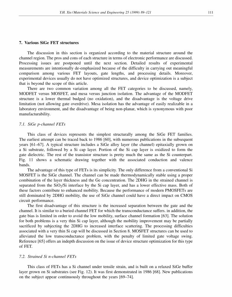
7.2. Strained Si n-channel FETs
This class of FETs has a Si channel under tensile strain, and is built on a relaxed SiGe bufferlayer grown on Si substrates (see Fig. 12). It was first demonstrated in 1986 [68]. New publicationson the subject appear continuously throughout the years [69±74].
Y.H. Xie / Materials Science and Engineering 25 (1999) 89±121 111
The enhanced 2DEG mobility and velocity overshoot are expected to result in an increasedtransconductance for n-channel FETs. Such enhancement has been demonstrated by comparingdevices with strained Si channel to the control devices with conventional unstrained Si channel [75].The strained Si channel can be oxidized to form conventional gate stack.
The most serious challenge this device faces is the dislocations associated with the relaxedbuffer layer. Each dislocation half loop consists of two threading dislocation segments, and onemisfit dislocation segment [76]. The misfit segment is necessary for the strain relaxation, while thethreading segments are responsible for the degradation of electronic properties. Threadingdislocations under the gate area of a MOSFET could affect the threshold voltage and the gateoxide integrity, whereas the ones under the source/drain areas could cause pn junction leakage.
Fig. 11. Schematic drawing (A) and the energy band diagram along the dotted line (B) of a SiGe p-channel MOSFET. Thefunction of the p+ doped layer is for threshold voltage adjustment. It is a buried channel FET. The only layer that is understrain is the SiGe channel.
112 Y.H. Xie / Materials Science and Engineering 25 (1999) 89±121
Typical threading dislocation density in a compositionally graded, relaxed SiGe buffer layer is on theorder of 106 cmÿ2 [77]. Even the density in the most optimistic claim of 104 cmÿ2 [72] is manyorders of magnitude too high for the state of the art VLSI technology, which demands a density thatis lower than 1 cmÿ2. However, this higher than ideal dislocation density is not necessarily an
Fig. 12. Schematic drawing (A) and the energy band diagram along the dotted line (B) of a n-channel MOSFET with the Sichannel under tensile strain. Notice there is a sacrificial Si cap-layer that is oxidized to form gate oxide. From the banddiagram, it is obvious that this is again a buried channel device, and a surface channel will form under high enough gatebias.
Y.H. Xie / Materials Science and Engineering 25 (1999) 89±121 113

insurmountable hurdle for relaxed SiGe buffers. It is well known that clean dislocations notdecorated by point defects or impurities are electrically inactive. Moreover, there are approachesproposed to reduce the threading dislocation density, notably using patterned substrates [78]. This iscertainly an area of research that is worth pursuing if the relaxed SiGe buffer layer is ever to be usedin the VLSI technology.
7.3. Strained Si p-channel FETs
There have been a few attempts at using Si channels under tensile strain for PMOSFET [79,80]with positive results. Fig. 12 again provides a good reference for the current discussion. One needs toimagine that the p-type doping are reversed in this case. As a result, the band bending direction isalso reversed. Because of the similar valence band structure among the cubic semiconductors atÿ-point, it is reasonable to expect 2DHG is Si channels under tensile strain to possess similaradvantaged in electronic transport as in Ge channels under compressive strain, as has been discussedat the end of Section 6. One of the benefits is to allow complementary FET fabrication using thesame epitaxial structure.
The challenge discussed in Section 7.2 applies to this case as well. In addition, the valence bandline-up between the channel and the underlying buffer layer is in the `wrong' direction. In otherwords, the Si layer is a barrier, rather than a well, to the 2DHG. This requires a large gate biasvoltage, or a gate overdrive, to populate the surface (high mobility) channel. The reportedsubthreshold behavior of the transistor does seem to be counter-intuitively not affected by thepresence of the buried channel [81].
7.4. Compressively strained Ge (SiGe)-channel FETs
Fig. 13 shows the representative structure of the p-channel FETs Nearly all the publisheddevices are MOSFETs [82±85], presumably due to the difficulty of fabricating high quality gatedielectric on Ge. The virtue of this FET category includes lower 2DHG effective masses, andreduced intervalley scattering. The use of compressively strained SiGe, instead of pure Ge, channelallows the use of relaxed SiGe buffer layer with lower Ge composition, but adds alloy scattering intothe transport picture.
Compared to the strained Si channel devices, the final Ge composition in the relaxed bufferlayer has to be pushed higher in order to keep the strain in the Ge channel less than 1%. This meanssomewhat higher dislocation densities. Using SiGe channel instead circumvents the problem.Another problem is that a compressively strained layer tends to form 3D islands during epitaxialgrowths, as has been shown experimentally [51]. The rough surface of the channel inadvertentlyresults in lower carrier mobility [57]. This problem becomes especially prevalent when the Gechannel is grown directly on Si substrates [86]. The formation of 3D islands can be avoided bycontrolling the epitaxial growth kinetics.
7.5. Hetero-CMOSFETs
This is a new version of heterostructure FETs [87]. It is essentially a combination of theFETs discussed in Sections 7.2 and 7.4. The key advantage is the possibility of integrating n- andp-channel MOSFETs with the same heteroepitaxial layered structure, while utilizing the superiortransport properties of strained channels. There has been no published experimental realization, butextensive simulation studies have been done on the DC as well as circuit performance.
114 Y.H. Xie / Materials Science and Engineering 25 (1999) 89±121
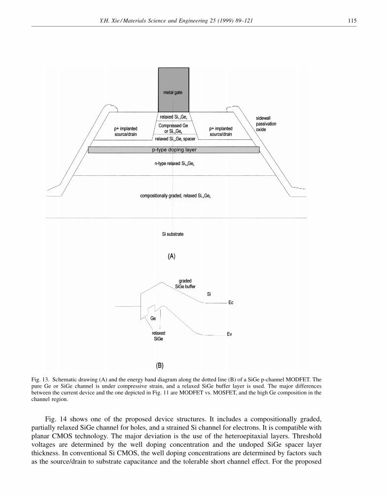
Fig. 14 shows one of the proposed device structures. It includes a compositionally graded,partially relaxed SiGe channel for holes, and a strained Si channel for electrons. It is compatible withplanar CMOS technology. The major deviation is the use of the heteroepitaxial layers. Thresholdvoltages are determined by the well doping concentration and the undoped SiGe spacer layerthickness. In conventional Si CMOS, the well doping concentrations are determined by factors suchas the source/drain to substrate capacitance and the tolerable short channel effect. For the proposed
Fig. 13. Schematic drawing (A) and the energy band diagram along the dotted line (B) of a SiGe p-channel MODFET. Thepure Ge or SiGe channel is under compressive strain, and a relaxed SiGe buffer layer is used. The major differencesbetween the current device and the one depicted in Fig. 11 are MODFET vs. MOSFET, and the high Ge composition in thechannel region.
Y.H. Xie / Materials Science and Engineering 25 (1999) 89±121 115
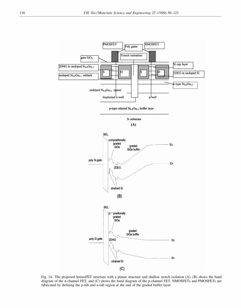
Fig. 14. The proposed heteroFET structure with a planar structure and shallow trench isolation (A). (B) shows the banddiagram of the n-channel FET, and (C) shows the band diagram of the p-channel FET. NMOSFETs and PMOSFETs arefabricated by defining the p-tub and n-tub region at the end of the graded buffer layer.
116 Y.H. Xie / Materials Science and Engineering 25 (1999) 89±121
heteroFET structure, simulation shows that the added constrains of threshold voltages on well dopinglevels do not significantly worsen short channels effects [88]. the low transconductance drawback ofthe buried channels is off set by enhanced mobilities and velocities. The combined transport propertyenhancements from n- and p-channel FETs give the CMOS circuit an estimated 4.6 times reductionin the power±delay product [88], and the toggle frequency of a 0.1 mm gate length T-flip-flop of upto 70 GHz [89]. Higher 2DEG and 2DHG mobilities at lower longitudinal electric field values allowsthe use of lower supply voltage while maintaining the same current drive. This features of theheteroFETs is responsible for the reduced power±delay product, making it attractive for portableelectronic applications.
The most serious roadblock for heteroFETs is the need for the relaxed SiGe buffer layer, and theassociated high dislocation density. It is indeed a challenge to reduce the threading dislocationdensity to near the 1 cmÿ2 level as required by today's VLSI technology. The other challenge is thecontrol of the sheet charge density in the n-SiGe layer. The main reason for this layer is to deflect theband bending in order to avoid the formation of a low mobility surface channel. However, the merepresence of this layer affects the threshold voltage of mainly the n-channel FETs. This boils down toa manufacturability issues that will be discussed in the next section.
8. Material and processing complexities
As can be expected, introducing Ge into the already mature Si VLSI technology faces manychallenges. This section discusses the material and processing related challenges. some of them areinherent to SiGe materials, and others are processing techniques dependent. In the followingdiscussion, issues inherent to SiGe materials are discussed first. Processing related issues are dividedaccording to major categories of Si VLSI processing technologies, namely, epitaxial growths,furnace operations, etching, and film deposition.
Two of the inherent SiGe material properties of concern are: narrower band gap andlower thermal conductivity, as compared to Si. For FET structures consisting of relaxed SiGebuffer layers, the narrower band gap of a relaxed Si0.7Ge0.3 causes an increase of the source/drain tosubstrate leakage current by about 150 times over that of Si [90], irrespective of the materialquality. This means for a given bias voltage, the standby power consumption of such a CMOScircuit is 150 times higher than the Si counterpart, a severe handicap for portable electronicsapplications. The thermal conductivity of relaxed Si0.7Ge0.3 is approximately 0.1 W/cm K [91],15 times lower than the Si value of 1.5 W/cm K [30]. A lower thermal conductivity causes devicesto be heated by its own power consumption, and is potential concern for high packing densitycircuits.
Dislocations are another quasi-inherent property of relaxed SiGe. Although high dislocationdensity is not synonymous with unstrained SiGe, it inevitably exists in relaxed SiGe on Si substrates.For a given misfit dislocation density, the density of threading dislocations is dependent on theepitaxial process and thermal cycles. It has been shown that threading dislocation densities can belowered dramatically by controlling the kinetics of the epitaxial growth [92]. However, the lowestthreading dislocation density ever reported is still on the order of 104 cmÿ2. This again meansincreased source/drain to substrate leakage current, as has been discussed in Section 7.2.
The first processing issue is epitaxy. The presence of Ge means strain, and strain means thedanger of having dislocation and 3D growth. In general, lower growth temperature and faster growthrate tend to minimize these problems, at the cost of higher point defect density. This constraint is inaddition to all the precautions necessary for the homoepitaxy of Si on Si.
Y.H. Xie / Materials Science and Engineering 25 (1999) 89±121 117
The discussion of furnace operations can be further divided into oxidation and diffusion. It hasbeen shown experimentally that Ge is snow-plowed at the oxide±crystalline interface by oxidizingSiGe alloy [93]. This problem can be largely circumvented if the Si supply at the reaction interface isslow compared to the oxidation rate [94]. Congruent SiO2 with a sharp interface has been obtainedthrough 7008C wet oxidation [95]. Because this conditions is so much different from the commonpractice in Si VLSI, people have been avoiding SiGe by using a Si cap layer for oxidation. Straindoes not seem to have a significant effect on the rate of oxidation of Si [96].
High temperature cycles during a furnace operation cause two types of diffusion: dopant andGe. Studies on Si interstitial assisted B diffusion indicate a diffusivity that is slower in SiGe [97],with minimal dependence of on strain [98]. Ge diffusion, on the other hand, is significant even atmoderate temperature of 7008C [99]. Interdiffusion between Ge and Si could result in the smearingof the heterointerface and consequently degraded transport properties. Overall, the use of SiGematerial imposes a restriction on the thermal budget, which may in turn impose limitation onconventional furnace operations such as thermal oxidation, and tub drive-in.
Etching is an important component of the Si VLSI technology. Majority of the etching steps arein a gaseous ambient, i.e. plasma enhanced vapor phase chemical reaction. Etch chemistry and etchstop are some of the crucial elements in dry etching. What has been used successfully for etching Siis more than likely to be inadequate for SiGe. While no systematic study in this regard can be foundin the literature, there seems to have no known fundamental roadblocks. As far as wet etching isconcerned, new chemistry is again needed. For example, a well known recipe for Si surface cleaning[100] etches SiGe at a very fast rate, and this can no longer be used for surface cleaning. On the otherhand, layers with and without Ge can be used as etch stops when proper chemistry is used [101].
Finally, the key issues in film deposition are adhesion and wafer warpage. There is again a lackof published literature on adhesion of various metal and dielectric films on SiGe. Thick relaxed SiGebuffer layers could potentially be a problem in terms of water warpage. Although the buffer layer isrelaxed, the thermal expansion coefficient difference between SiGe and Si could still cause thetypically microns thick SiGe film to exert stress on the Si wafer. This happens when the wafer iscooled after the epitaxial growth to below the temperature at which dislocation motion stops.
In summary, SiGe material has the inherent drawbacks of narrower band gap and smallerthermal conductivity as compared to Si. SiGe device processing also imposes many restrictions inevery major technological area including epitaxy, oxidation, diffusion, etching, and film deposition.There is no doubt that a lot of research and development effort is needed if SiGe is to be used in theVLSI technology. However, there appear to be no intrinsic physics limits present. It is likely that thesuccess of SiGe will depend on costs of implementation, return on investment, and timing for marketintroduction.
9. Summary and future perspective
Starting from a brief review of the basics of FETs and BJTs, we discuss typical applications ofthe two types of transistors, which is followed a FET performance analysis including thetransconductance, speed, power consumption, and packing density. These sections form thefoundation for the understanding of the pros and cons of strained SiGe FETs. Based on thisfoundation, we scrutinize the perceived advantages of using SiGe, review the array of SiGe FETstructures, and look at material and processing challenges.
The key FET performance parameter we have been focusing on is the transconductance. UsingSiGe, the FET extrinsic transconductance has been shown to improve by about 50% over the Si
118 Y.H. Xie / Materials Science and Engineering 25 (1999) 89±121
counterpart (with a 75% improvement in the electron mobility) [103], which is comparable to thedifference between one generation of Si VLSI technology. The transconductance enhancementenables increased circuit speed, packing density, or decreased power consumption.
Investment in research and development is needed in most areas of the VLSI technology. Somefundamental problems such as higher leakage current due to band gap narrowing, and devicereliability issues related to hot carrier degradation and dislocations, will have to be minimizedthrough device structure optimization. Looking at the historic development of the Si VLSItechnology, it seems that SiGe FETs will have their best chance of becoming a part of the technologywhen Si FETs run into serious obstacles. Obstacles such as the cost of equipment or thetechnological difficulty along the path of the continued shrinking could render SiGe FETs a viablealternative.
In terms of scientific challenges, we see the immediate need of understanding the kinetic pathtowards obtaining totally relaxed SiGe buffer layers with much reduced threading dislocationdensities. Alternatively, the know-how in fabricating high quality SiGe substrates could become thesolution for the problem of dislocations. From the electronic transport point of view, the subject ofvelocity overshoot deserves more study and understanding. Finally, p-channel FETs have notreceived the amount of attention it rightfully deserve, in view of the much slower PMOSFET in theSi CMOS technology.
With the rapid progress in the understanding of SiGe devices, it is hopeful that SiGe will oneday become part of the VLSI technology.
Acknowledgements
The author would like to thank Dr. Kwok K. Ng, Dr. Don P. Monroe, Dr. Cliff A. King, andProf. Eugene A. Fitzgerald for many helpful discussions.
References
[1] E. Kasper, H.J. Herzog, Appl. Phys. 8 (1975) 199.[2] J.C. Bean, L.C. Feldman, A.T. Fiory, S. Nakahara, J.K. Robinson, J. Vac. Sci. Technol. A2 (1984) 436.[3] J.C. Bean, T.T. Sheng, L.C. Feldman, A.T. Fiory, R.T. Lynch, Appl. Phys. Lett. 44 (1984) 102.[4] G. Abstreiter, H. Brugger, T. Wolf, H. Jorke, H.J. Herzog, Phys. Rev. Lett. 54 (1985) 2441.[5] H. Dambkes, H.J. Herzog, H.Jorke, H. Kibbel, E. Kasper, IEDM Tech. Dig. (1985) 768.[6] T.P. Pearsall, J.C. Bean, IEEE Electron. Dev. Lett. EDL-7 (1986) 308.[7] S. Luryi, T.P. Pearsall, H. Temkin, J.C. Bean, Electron. Dev. Lett. EDL-7 (1986) 104.[8] C. Lee, K.L. Wang, Appl. Phys. Lett. 60 (1992) 2264.[9] C.A. King, R.W. Johnson, Y.K. Chen, T.Y. Chiu, R.A. Cirelli, G.M. Chin, M.R. Frei, A. Kornblit, G.P. Schwartz,
IEDM Tech. Dig. (1995) 751.[10] D. Harame, L. Larson, M. Case, S. Kovacic, S. Voinigescu, T.Tewksbury, D. Nguyen-Ngoc, K. Stein, J. Cressler, S.J.
Jeng. J. Malinowski, R. Growves, E. Eld, D. Sunderland, D. Rensch, M. Gilbert, K. Schonenberg, D. Ahlgren, S.Rosenbaum, J. Glenn, and B. Meyerson, IEDM Tech. Dig. (1995) 731.
[11] A. Schuppen, U. Erben, A. Gruhle, H. Kibbel, H. Schumacher, U. Konig, IEDM Tech. Dig. (1995) 743.[12] C.G. Van de Walle, R.M. Martin, Phys. Rev. B 34 (1986) 5621.[13] S. Fukatsu, H. Akiyama, Y. Shraki, H. Sakaki, J. Crystal Growth 157 (1995) 1.[14] D.C. Houghton, J. Appl. Phys. 70 (1991) 2136.[15] R. Hull, J.C. Bean, D.J. Werder, R.E. Leibenguth, Appl. Phys. Lett. 52 (1988) 1605.[16] E.A. Fitzgerald, Y.H. Xie, D. Monroe, P.J. Silverman, J.M. Kuo, A.R. Kortan, F.A. Thiel, B.E. Weir, J. Vac. Sci.
Technol. B10 (1992) 1807.[17] A.C. Churchill, D.J. Robbins, D.J. Wallis, N. Griffin, D.J. Paul, A.J. Pidduck, Semicond. Sci. Technol. 12 (1997)
Y.H. Xie / Materials Science and Engineering 25 (1999) 89±121 119
943.[18] G. Abstreiter, H. Brugger, T. Wolf, H. Jorke, H.J. Herzog, Phys. Rev. Lett. 54 (1985) 2441.[19] Y.J. Mii, Y.H. Xie, E.A. Fitzgerald, F.B.E. Weir, L.C. Feldman, Appl. Phys. Lett. 59 (1991) 1611.[20] K. Ismail, M. Arafa, K.L. Saenger, J.O. Chu, B.S. Meyerson, Appl. Phys. Lett. 66 (1995) 1077.[21] X Don Monroe, Y.H. Xie, Y.E.A. Fitzgerald, P.J. Silverman, Phys. Rev. B46 (1992) 7935.[22] J.C. Sturm, H. Manoharan, L.C. Lenchyshyn, M.L. Thewalt, N.L. Rowell, J.P. Noel, D.C. Houghton, Phys. Rev.
Lett. 66 (1991) 1362.[23] H. Sunamura, N. Usami, Y. Shiraki, S. Fukatsu, Appl. Phys. Lett. 66 (1995) 3024.[24] J.E. Lilienfeld, Method and apparatus for controlling electric currents, US Patent No. 1,745,175; filed 1926, granted
1930.[25] J.E. Lilienfeld, Device for controlling electric currents, US Patent No. 1,900,018; filed 1928, granted 1933.[26] J.E. Lilienfeld, Amplifier for electric current, US Patent No. 1,877,140; filed 1928, granted 1932.[27] C.T. Sah Evolution of the MOS transistor from conception to VLSI, Proc. IEEE 76 (1988) 1280.[28] M.M. Atalla, M. Tannenbaum, E.J. Scheibner Stabilization of silicon surface by thermally grown oxides, Bell Syst.
Tech. J. 38 (1959) 123.[29] K.K. Ng, Complete Guide to Semiconductor Devices, McGraw-Hill, New York, 1995.[30] S.M. Sze, Physics of Semiconductor Devices, 2nd ed., Wiley, New York, 1981.[31] C.T. Sah, Fundamentals of Solid State Electronics, World Scientific, Singapore, 1991.[32] G. Moore VLSI: what does the future hold?, Electron. Aust. 42 (1980) 14.[33] P. Smith, M. Inoue, J. Frey Electron velocity in Si and GaAs at very high electric fields, Appl. Phys. Lett. 37 (1980)
797.[34] W. Shockley, Bell System Tech. J. 28 (1949) 436.[35] D. Harame, Proc. IEEE BCTM (1997) 36.[36] E.J. Prinz, J.C. Sturm, IEDM Tech. Dig. (1991) 853.[37] C.T. Kirk, IEEE Trans. Electron. Dev. ED-9 (1962) 164.[38] Y.P. Tsividis, IEEE J. Solid State Circuit 133 (1978) 383.[39] J. Min, A. Rofougaran, H. Samueli, A.A. Abidi, Proc. Custom IC Conf., San Diego, CA, 1994, p. 379.[40] A.G. Sabnis, J.T. Clemens, IEDM Tech. Dig. (1979) 18.[41] S. Takagi, M. Iwase, A. Toriumi, IEDM Tech. Dig. (1988) 398.[42] Figure Complied by Don Monroe.[43] G.G. Shahidi, D.A. Antoniadis, H.I. Smith, IEEE Electron. Dev. Lett. 9 (1988) 94.[44] D. Sinitsky, F. Assaderaghi, M. Orshansky, J. Bokor, C. Hu, Solid State Electron. 41 (1997) 1119.[45] J.B. Roldan, F. Gamiz, J.A. Lopez-Villanueva, J.E. Carceller, J. Appl. Phys. 80 (1996) 5121.[46] M.R. Pinto, E. Sangiorgi, J. Bude, IEEE Electron. Dev. Lett. EDL-14 (1993) 375.[47] M.V. Fischetti, S.E. Laux, IEEE Trans. Electron. Dev. 38 (1991) 650.[48] T. Mizuno, R. Ohba, K. Ohuchi, Appl. Phys. Lett. 69 (1996) 106.[49] J.W. Matthews, A.E. Blakeslee, J. Crystal Growth 27 (1974) 118.[50] D.J. Eagleshman, M. Cerullo, Phys. Rev. Lett. 64 (1990) 1943.[51] Y.H. Xie, G.H. Gilmer, C. Roland, P.J. Silverman, S.K. Buratto, J.Y. Cheng, E.A. Fitzgerald, A.R. Kortan, S.
Schuppler, M.A. Marcus, P.H. Citrin, Phys. Rev. Lett. 74 (1995) 4963.[52] J. Tersoff, C. Teichert, M.G. Lagally, Phys. Rev. Lett. 76 (1996) 1675.[53] T.B. Massalski, J.L. Murray, L.H. Bennett, H. Baker (Eds.), Binary Alloy Phase Diagrams, American Society for
Metals, Metals Park, Ohio, 1986.[54] J. Welser, J.L. Hoyt, S. Takagi, J.F. Gibbons, IEDM Tech. Dig. (1994) 373.[55] K. Ismail, S.F. Nelson, J.O. Chu, B.S. Meyerson, Appl. Phys. Lett. 63 (1993) 660.[56] G. Bastard, Wave Mechanics Applied to Semiconductor Heterostructures, Les Editions de Physique, Paris, France,
1992.[57] Y.H. Xie, D. Monroe, E.A. Fitzgerald, P.J. Silverman, F.A. Thiel, G.P. Watson, Appl. Phys. Lett. 63 (1993) 2263.[58] S. Takagi, J.L. Hoyt, J. Welser, J.F. Gibbons, J. Appl. Phys. 803 (1996) 1567.[59] H. Miyata, T. Yamada, D.K. Ferry, Appl. Phys. Lett. 62 (1993) 2661.[60] T.P. Pearsall, J.C. Bean, IEEE Electron. Dev. Lett. 7 (1986) 308.[61] D.K. Nayak, J.C.S. Woo, J.S. Park, K.L. Wang, K.P. Mac Williams, IEEE Electron. Dev. Lett. 12 (1991) 154.[62] S. Verdonckt-Vandebroek, E.F. Crabbe, B.S. Meyerson, D.L. Harame, P.J. Restle, J.M.C. Stork, A.C. Megdanis,
C.L. Stanis, A.A. Bright, G.M..W. Kroesen, A.C. Warren, Proc. Symp. VLSI Technol. (1991) 105.[63] P.M. Garone, V. Venkataraman, J.C. Sturm, IEEE Electron. Dev. Lett. 12 (1991) 230.[64] V.P. Kesan, S. Subbanna, P.J. Restle, M.J. Tejwani, J.M. Aitken, S.S. Lyer, J.A. Ott, IEDM Tech. Dig. (1991) 373.[65] K. Goto, J. Murota, T. Maeda, R. Schutz, K. Aizawa, R. Kircher, K. Yokoo, S. Ono, Jpn. J. Appl. Phys. 32 (1993)
438, Part I.[66] S. Verdonckt-Vandebroek, E.F. Crabbe, B.S. Meyerson, D.L. Harame, P.J. Restle, J.M.C. Stork, J.B. Johnson, IEEE
Trans. Electron. Dev. 41 (1994) 90 .[67] P.W. Li, E.S. Yang, Y.F. Yang, J.O. Chu, B.S. Meyerson, IEEE Electron. Dev. Lett. 15 (1994) 402.
120 Y.H. Xie / Materials Science and Engineering 25 (1999) 89±121
[68] H. Daembkes, H. Herzog, H. Jorke, H. Kibbel, E. Kasper, IEEE Trans. Electron. Dev. ED-33 (1986) 633.[69] R.W. Keyes, IEEE Trans. Electron. Dev. ED-33 (1986) 863.[70] U. Konig, F. Schaffler, Electron. Lett. 27 (1991) 1405.[71] U. Konig, A.J. Boers, F. Schaffler, E. Kasper, Electron. Lett. 28 (1992) 160.[72] K. Ismail, B.S. Meyerson, S. Rishton, J.O. Chu, S.F. Nelson, J. Nocera, IEEE Electron. Dev. Lett. 13 (1992) 229.[73] K. Ismail, S. Rishton, J.O. Chu, K. Chan, B.S. Meyerson, IEEE Electron. Dev. Lett. 14 (1993) 348.[74] J. Welser, J.L. Hoyt, S. Takagi, J.F. Gibbons, IEDM Technical Digest (1994) 373.[75] J. Welser, J.L. Hoyt, J.F. Gibbons, IEEE Electron. Dev. Lett. 15 (1994) 100.[76] Y.H. Xie, E.A. Fitzgerald, P.J. Silverman, Mat. Sci. Eng. B30 (1995) 201.[77] G.P. Watson, E.A. Fitzgerald, Y.H. Xie, Don Monroe, J. Appl. Phys. 75 (1994) 263.[78] E.A. Fitzgerald, Y.H. Xie, D. Brasen, M.L. Green, J. Michel, P.E. Freeland, B.E. Weir, J. Electron. Mat. 19 (1990)
949.[79] D.K. Nayak, J.C.S. Woo, J.S. Park, K.L. Wang, K.P. MacWilliams, Appl. Phys. Lett. 62 (1993) 2853.[80] J. Welser, J.L. Hoyt, J.F. Gibbons, IEDM Tech. Dig. (1992) 1000.[81] D.K. Nayak, J.C.S. Woo, J.S. Park, K.L. Wang, K.P. Mac Williams, Jpn. J. Appl. Phys. 33 (1994) 2412.[82] E. Murakami, K. Nakagawa, A. Nishida, M. Miyao, IEEE Electron. Dev. Lett. 12 (1991) 71.[83] U. Konig, F. Schaffler, IEEE Electron. Dev. Lett. 14 (1993) 205.[84] M. Arafa, K. Ismail, P. Fay, J.O. Chu, B.S. Meyerson, I. Adesida, Electron. Lett. 31 (1995) 680.[85] I. Adesida, M. Arafa, K. Ismail, J.O. Chu, B.S. Meyerson, Microelectron. Eng. 35 (1997) 257.[86] B.R. Cyca, K.G. Robins, N.G. Tarr, D.X. Xu, J.P. Noel, D. Landheer, M. Simard-Normandin, J. Appl. Phys. 81
(1997) 8079.[87] U. Konig, F. Schaffler, Proc. Int. Conf. Solid State Dev. & Mat. (SSDM), 1993, p. 201.[88] A. Sadek, K. Ismail, M.A. Armstrong, D.A. Antoniadis, F. Stern, IEEE Trans. Electron. Dev. 43 (1996) 1224.[89] R. Hagelauer, T. Ostermann, U. Konig, M. Gluck, G. Hock, Electron. Lett. 33 (1997) 208.[90] J.J. Welser, Proc. MRS'95.[91] J.P. Dismukes, L. Ekstrom, E.F. Steigmeier, I. Kudman, D.S. Beers, J. Appl. Phys. 35 (1964) 2899.[92] G. Kissinger, T. Morgenstern, G. Morgenstern, H. Richter, Appl. Phys. Lett. 66 (1995) 2083.[93] O.W. Holland, C. White, D. Fathy, Appl. Phys. Lett. 51 (1987) 520.[94] D.C. Paine, C. Caragianis, A.F. Schwartzman, J. Appl. Phys. 70 (1991) 5076.[95] W.S. Liu, E.W. Lee, M.A. Nicolet, V. Arbet-Engels, K.L. Wang, N.M. Abuhadba, C.R. Aita, J. Appl. Phys. 71
(1992) 4015.[96] J. Welser, J.L. Hoyt, J.F. Gibbons, Jpn. J. Appl. Phys. 33 (1994) 2419.[97] P. Kuo, J.L. Hoyt, J.F. Gibbons, J.E. Turner, D. Lefforge, Appl. Phys. Lett. 66 (1995) 580.[98] P. Kuo, J.L. Hoyt, J.F. Gibbons, J.E. Turner, D. Lefforge, Appl. Phys. Lett. 67 (1995) 706.[99] D.J. Lockwood, J.M. Baribeau, P.Y. Timbrell, J. Appl. Phys. 65 (1989) 3049.
[100] W. Kern The recipe calls for alternative immersion in NH4OH, The recipe calls for alternative immersion inNH4OH and H2SO4 solutions, RCA Rev. 31 (1970) 234.
[101] T.K. Carns, M.O. Tanner, K.L. Wang, J. Electrochem. Soc. 142 (1995) 1260.[102] H.C. Pao, C.T. Sah, Solid State Electron. 9 (1996) 927.[103] K. Rim, J.L. Hoyt, J.F. Gibbons, IEDM Tech. Dig. (1998) 707.
Y.H. Xie / Materials Science and Engineering 25 (1999) 89±121 121