Field effect transistors
6
Prepare for GATE/PSU for free log on: www.testindia24x7.com Field Effect Transistors The operation of the field effect transistor (FET) can be explained in terms of only majority carrier (one Polarity) charge flow; the Transistor is therefore called unipolar. Two kinds of field effect devices are widely used, the junction field effect transistor (JFET) and the metal oxide semiconductor Field effect Transistor (MOSFET) Construction and Symbols of the JFET Physical arrangements and symbols of the JFET are shown in fig Conduction is passage of charge carriers from source (S) to drain (D) through the path (channel) between the gate elements. GATE| SSC-JEN |PSU’S|STATE ENGINEERING EXAMINATION 502 Behind Mahaveer Nagar Durgapura Mob: +91-9982030151, 9571368040 Web: www.engineeringmasters.in ,email: [email protected] JFET BJT Source (S) emitter (E) Drain (D) Collector (C ) gate (G) Base (B) Drain supply (Vdd) Collector supply (Vcc) gate supply (Vdd) Base supply (Vbb) drain current (iD) Collector current (ic)
-
Upload
wwwengineeringmastersin -
Category
Engineering
-
view
286 -
download
4
Transcript of Field effect transistors

Prepare for GATE/PSU for free log on: www.testindia24x7.com
Field Effect Transistors
The operation of the field effect transistor (FET) can be explained in terms of only majority carrier (one Polarity) charge flow; the Transistor is therefore called unipolar. Two kinds of field effect devices are widely used, the junction field effect transistor (JFET) and the metal oxide semiconductor Field effect Transistor (MOSFET)
Construction and Symbols of the JFET
Physical arrangements and symbols of the JFET are shown in fig Conduction is passage of charge carriers from source (S) to drain (D) through the path (channel) between the gate elements.
The transistor can be n-channel (conduction by electrons) or p-channel (conduction by holes) and discussion of n-channel applies to p-channel devices if complementary (opposite in sign) voltages and currents are used. Analogies between the JFET and the BJT are shown in above table. Current and voltage symbology for FETs parallels.
GATE| SSC-JEN |PSU’S|STATE ENGINEERING EXAMINATION502 Behind Mahaveer Nagar Durgapura Mob: +91-9982030151, 9571368040
Web: www.engineeringmasters.in ,email: [email protected]
JFET BJT
Source (S) emitter (E)
Drain (D) Collector (C )
gate (G) Base (B)
Drain supply (Vdd) Collector supply (Vcc)
gate supply (Vdd) Base supply (Vbb)
drain current (iD) Collector current (ic)

Prepare for GATE/PSU for free log on: www.testindia24x7.com
Terminal Characteristics of the JFET
The JFET is almost applied in the common source (CS) two port arrangement of .where Vgs maintains a reverse bias of the gate source p-n junction. The resulting gate leakage current is negligibly small for most analysis (usually less than 1μA), allowing the gate to be treated as an open circuit. Thus, no input characteristic curves are necessary.
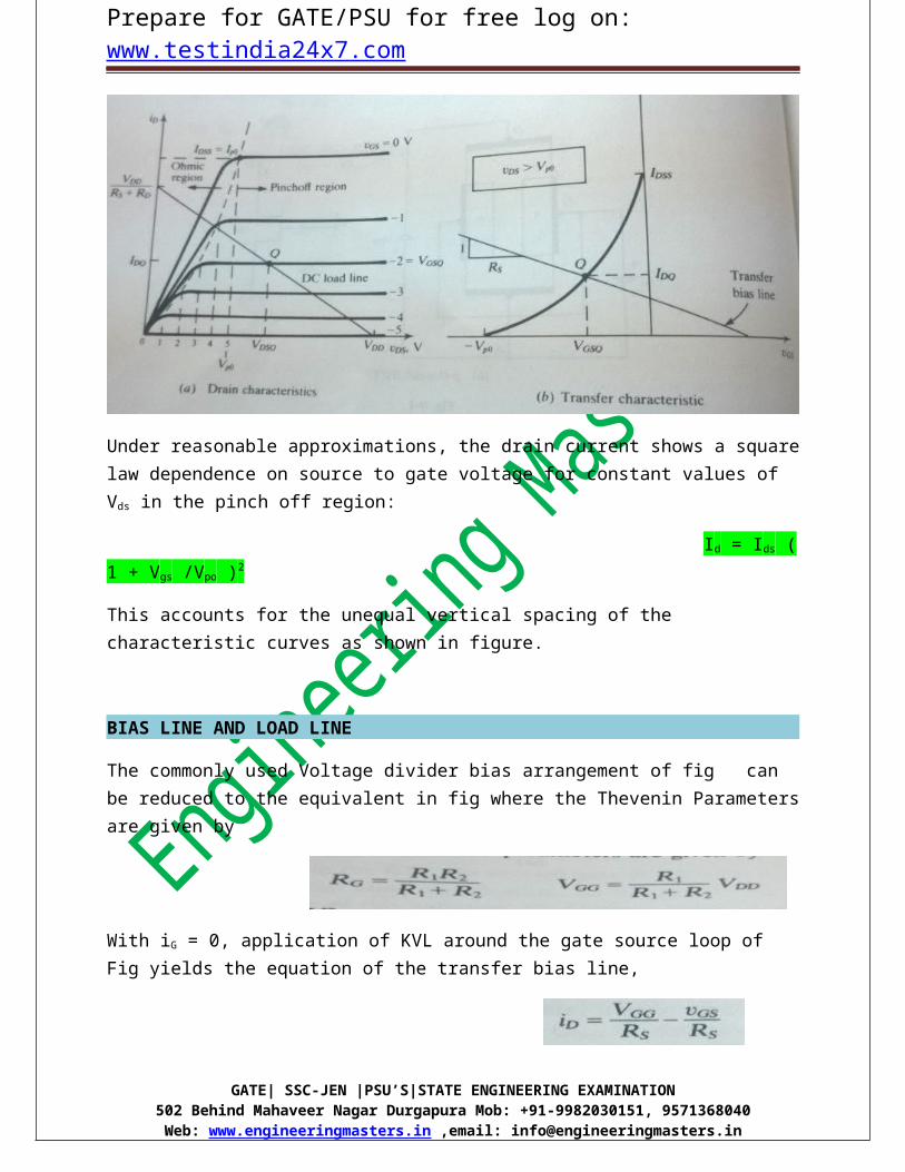
Output or drain characteristics of the n-channel JFET in CS connection are given shown in fig. if Vgs ˂ 0.For a constant value of Vgs ,the JFET acts as a linear resistive device (ohmic region) until the depletion region of the reverse –biased gate-source junction extends the width of the channel (a condition called pinch off). Above Pinchoff, but below avalanche breakdown, drain current id remains nearly constant as Vds is increased. For specification purpose the shorted gate parameters Idss and Vpo are defined as indicated in fig .Typically ,Vpo is between 4 and 5 V.As gate potential decreases, the source to drain voltage at which pinch off occurs (Vp) also decreases, approximately obeying the equation
Vp = Vpo + Vgs
Under reasonable approximations, the drain current shows a square law dependence on source to gate voltage for constant values of Vds in the pinch off region:
Id = Ids ( 1 + Vgs /Vpo )2
This accounts for the unequal vertical spacing of the characteristic curves as shown in figure.
BIAS LINE AND LOAD LINE
GATE| SSC-JEN |PSU’S|STATE ENGINEERING EXAMINATION502 Behind Mahaveer Nagar Durgapura Mob: +91-9982030151, 9571368040
Web: www.engineeringmasters.in ,email: [email protected]
Prepare for GATE/PSU for free log on: www.testindia24x7.com
The commonly used Voltage divider bias arrangement of fig can be reduced to the equivalent in fig where the Thevenin Parameters are given by
With iG = 0, application of KVL around the gate source loop of Fig yields the equation of the transfer bias line,
Which can be solved simultaneously with or plotted as indicated on fig to yield IDQ and VGSQ ,two of necessary three quiescent variables.
KVL around the drain source loop of fig leads to the equation of the dc load line,
Which when plotted on the drain characteristics of fig yields the remaining quiescent value VDSQ.Alternatively, with IDQ already determined,
CONSTRUCTION AND SYMBOLS OF THE MOSFET
GATE| SSC-JEN |PSU’S|STATE ENGINEERING EXAMINATION502 Behind Mahaveer Nagar Durgapura Mob: +91-9982030151, 9571368040
Web: www.engineeringmasters.in ,email: [email protected]

Prepare for GATE/PSU for free log on: www.testindia24x7.com
The n-Channel MOSFET has only a single p region (called the substrate), one side of which acts as a conducting channel. A metallic gate is separated by an insulating metal oxide (usually SiO2),when the name insulated –gate FET (IGFET) for the device. The p-channel MOSFET formed by interchanging p and n semiconductor material is described by complementary voltages and currents.
TERMINAL CHARACTERISTICS OF A MOSFET
In a channel MOSFET, the gate (positive plate), metal oxide film (dielectric), and substrate (negative Plate) form a capacitor, the electric field of which controls channel resistance. When the positive potential of the gate reaches threshold voltage VT (typically 2 to 4 V) sufficient free electrons are attracted to the region immediately beside the metal oxide film (this is called enhancement-mode operation) to induced a conducting channel of low resistivity. If the source to drain voltage is increased, the enhanced channel is depleted of free charge carriers in the area near the drain and pinch off occurs as in the JFET.Typical drain and transfer Characteristics are displayed in above figure.
GATE| SSC-JEN |PSU’S|STATE ENGINEERING EXAMINATION502 Behind Mahaveer Nagar Durgapura Mob: +91-9982030151, 9571368040
Web: www.engineeringmasters.in ,email: [email protected]