
SiC Workshop. EPE 2005, September 12 ESCAPEE Project 1 ESCAPEE EPE 2005 Dresden.
34
SiC Workshop. EPE 2005, September 12 ESCAPEE Project 1 ESCAPEE EPE 2005 Dresden EPE 2005 Dresden
-
Upload
stewart-parsons -
Category
Documents
-
view
222 -
download
0
Transcript of SiC Workshop. EPE 2005, September 12 ESCAPEE Project 1 ESCAPEE EPE 2005 Dresden.
SiC Workshop. EPE 2005, September 12 ESCAPEE Project
1
ESCAPEE
EPE 2005 DresdenEPE 2005 Dresden
SiC Workshop. EPE 2005, September 12 ESCAPEE Project
2
The achievements of the EC funded project "Establish Silicon Carbide Applications for Power
Electronics in Europe" (ESCAPEE)
J. Millan1, P. Godignon1, D. Tournier1, P.A. Mawby2, S. Wilks2, O.J. Guy2, and L. Chen2, R. Bassett3, A. Hyde3, N. Martin4, M. Mermet-Guyennet4, S. Pasugcio4, S. P M. Syväjärvi5, R.R. Ciechonski5, R. Yakimova5, L. Roux6,
F. Torregrosa6, T. Bouchet6, J-M. Bluet7, G. Guillot7, D. Hinchley8, S. Jones8, J. Rhodes8, P. Taylor9 and P. Waind9
1Centro Nacional de Microelectrónica, Campus Universidad Autónoma de Barcelona, 2School of Engineering, University of Wales Swansea,
3ALSTOM Research & Technology Centre, 4ALSTOM Transport SA, 5Department of Physics and Measurement Technology, Linköping
University, Sweden, 6Ion Beam Services, 7Institut National des Sciences Appliquées de Lyon, Laboratoire de Physique de la Matiere CNRS,
8Semelab Plc, 9Dynex Semiconductor Ltd.
SiC Workshop. EPE 2005, September 12 ESCAPEE Project
3
Overview
• Overview of recent results from the ESCAPEE project.• Update to the information originally presented at EPE
2003 in Toulouse. • Key targets• Significant scientific progresses
• Final achievements and successes.
SiC Workshop. EPE 2005, September 12 ESCAPEE Project
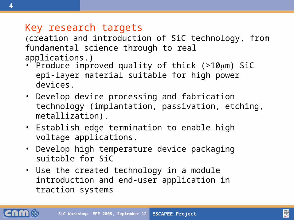
4
Key research targets (creation and introduction of SiC technology, from fundamental science through to real applications.)
• Produce improved quality of thick (>10m) SiC epi-layer material suitable for high power devices.
• Develop device processing and fabrication technology (implantation, passivation, etching, metallization).
• Establish edge termination to enable high voltage applications.
• Develop high temperature device packaging suitable for SiC
• Use the created technology in a module introduction and end-user application in traction systems

SiC Workshop. EPE 2005, September 12 ESCAPEE Project
5
Important scientific progressesSignificant results from the ESCAPEE project include:
Development of new sublimation epitaxial growth technique - produces epi-layers at growth rates up to 20 times faster than standard CVD growth.
Development of high temperature implantation equipment for SiC and the subsequent commercialisation.
Development of surface cleaning processes and reduction of surface damage produced by high temperature annealing, for implant activation.
Development of low resistance n-type and p-type ohmic contacts and high quality Schottky diodes.
Design of edge termination and fabrication of thermally stable Schottky diodes with blocking voltages of up to 4.7kV and reverse leakage currents of less than 2e-7 A/cm2 at 3.5kV.
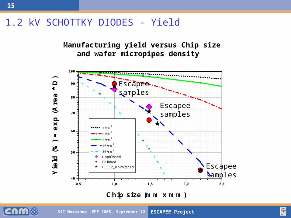
Increased device yield of 1.6mm 1.6mm diodes from 12% to 43% using a novel polishing technique.
SiC Workshop. EPE 2005, September 12 ESCAPEE Project
6
Significant results from the ESCAPEE project continued…
Development of 1.2 kV MOSFETs.
Record Field-effect mobility and drain current as a function of gate voltage for transistors with a PVT grown epilayer and a reference CVD grown epilayer.
Design and production of specialized high temperature thermally stable packaging for high voltage SiC devices.
Production of a demonstrator module using SiC diodes and Si IGBTs.
SiC Workshop. EPE 2005, September 12 ESCAPEE Project
7
ESCAPEE Technological developments
SiC Workshop. EPE 2005, September 12 ESCAPEE Project
8
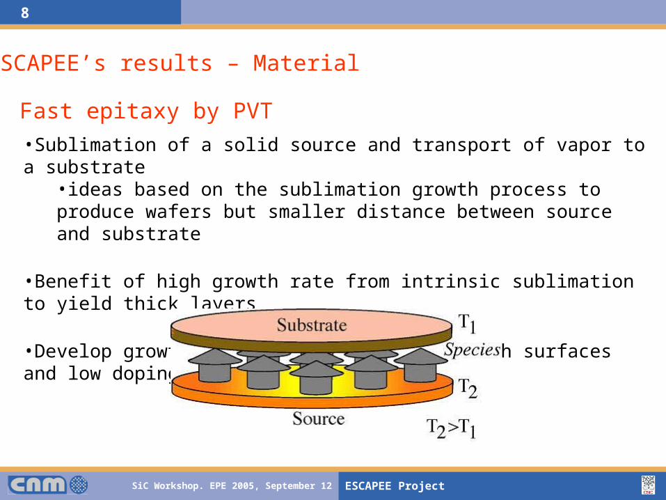
•Sublimation of a solid source and transport of vapor to a substrate •ideas based on the sublimation growth process to produce wafers but smaller distance between source and substrate
•Benefit of high growth rate from intrinsic sublimation to yield thick layers
•Develop growth conditions to achieve smooth surfaces and low doping
Fast epitaxy by PVT
ESCAPEE’s results – Material
SiC Workshop. EPE 2005, September 12 ESCAPEE Project
9
0
0,01
0,02
0,03
0,04
0
50
100
150
200
250
-5 0 5 10 15 20 25 30
Gate voltage [V]
PVT
CVD
tox
= 1550 Å,
L = 20 m, W= 100 m
CVD, ID
PVT, ID
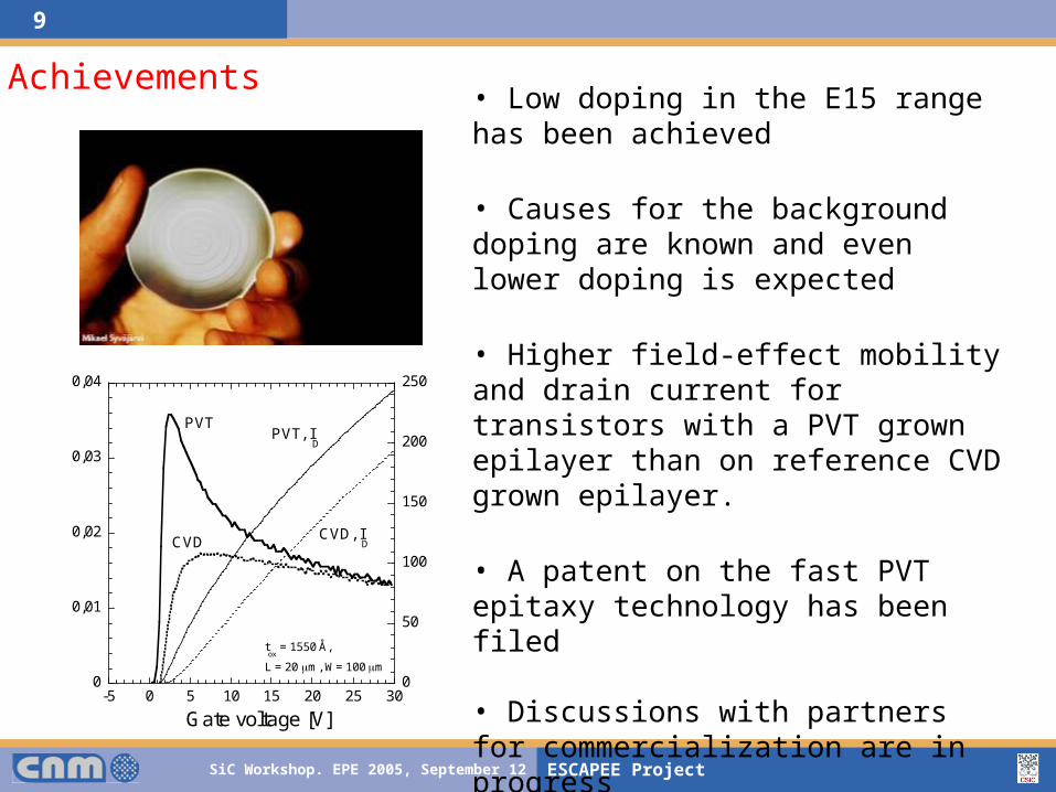
• Low doping in the E15 range has been achieved
• Causes for the background doping are known and even lower doping is expected
• Higher field-effect mobility and drain current for transistors with a PVT grown epilayer than on reference CVD grown epilayer.
• A patent on the fast PVT epitaxy technology has been filed
• Discussions with partners for commercialization are in progress
Achievements
SiC Workshop. EPE 2005, September 12 ESCAPEE Project
10
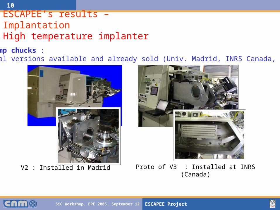
ESCAPEE’s results – Implantation
High temperature implanter
High temp chucks : - Several versions available and already sold (Univ. Madrid, INRS Canada, LETI.)
V2 : Installed in Madrid Proto of V3 : Installed at INRS (Canada)
SiC Workshop. EPE 2005, September 12 ESCAPEE Project
11
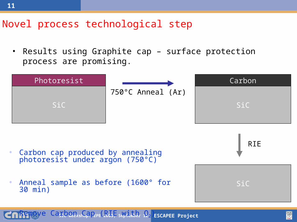
• Results using Graphite cap – surface protection process are promising.
SiC
Photoresist
SiC
Carbon
SiC
RIE
750°C Anneal (Ar)
• Carbon cap produced by annealing photoresist under argon (750°C)
• Anneal sample as before (1600° for 30 min)
• Remove Carbon Cap (RIE with O2)
Novel process technological step

SiC Workshop. EPE 2005, September 12 ESCAPEE Project
12
Carbon cap experiment
Surface roughness reduced by up to a factor of 10Improved forward I(V) characteristicsImproved reverse leakage currents
(a) (b)
C-cap protectedNot protected
SiC Workshop. EPE 2005, September 12 ESCAPEE Project
13
1.2 kV SCHOTTKY DIODES
SiC Workshop. EPE 2005, September 12 ESCAPEE Project
14
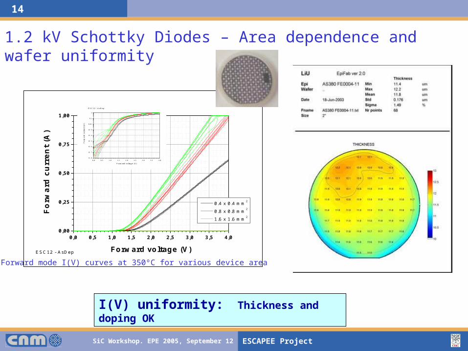
1.2 kV Schottky Diodes – Area dependence and wafer uniformity
Forward mode I(V) curves at 350ºC for various device area
I(V) uniformity: Thickness and doping OK
0,0 0,5 1,0 1,5 2,0 2,5 3,0 3,5 4,00,00
0,25
0,50
0,75
1,00
0.4 x 0.4 mm2
0.8 x 0.8 mm2
1.6 x 1.6 mm2
0,0 0,5 1,0 1,5 2,0 2,5 3,0 3,5 4,01E-8
1E-7
1E-6
1E-5
1E-4
1E-3
0,01
0,1
1
Fo
rwa
rd c
urr
en
t (A
)
Forward voltage (V)
ESC12 - AsDep
Fo
rwa
rd c
urr
en
t (A
)
Forward voltage (V)ESC12 - AsDep
SiC Workshop. EPE 2005, September 12 ESCAPEE Project
15
Manufacturing yield versus Chip size and wafer micropipes density
0,5 1,0 1,5 2,0 2,540
50
60
70
80
90
100
Chip size (mm x mm)
Yie
ld (
%)
= e
xp (
Are
a *
D)
1/cm2
5/cm2
2/cm2
16/cm2
30/cm2
Unpolished Polished ESC12_UnPolished
1.2 kV SCHOTTKY DIODES - Yield
Escapee samples
Escapee samples
Escapee samples
SiC Workshop. EPE 2005, September 12 ESCAPEE Project
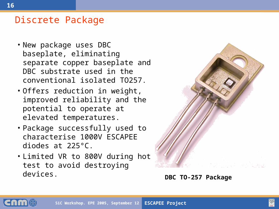
16
Discrete Package
• New package uses DBC baseplate, eliminating separate copper baseplate and DBC substrate used in the conventional isolated TO 257.
• Offers reduction in weight, improved reliability and the potential to operate at elevated temperatures.
• Package successfully used to characterise 1000V ESCAPEE diodes at 225°C.
• Limited VR to 800V during hot test to avoid destroying devices.
DBC TO-257 Package
SiC Workshop. EPE 2005, September 12 ESCAPEE Project
17
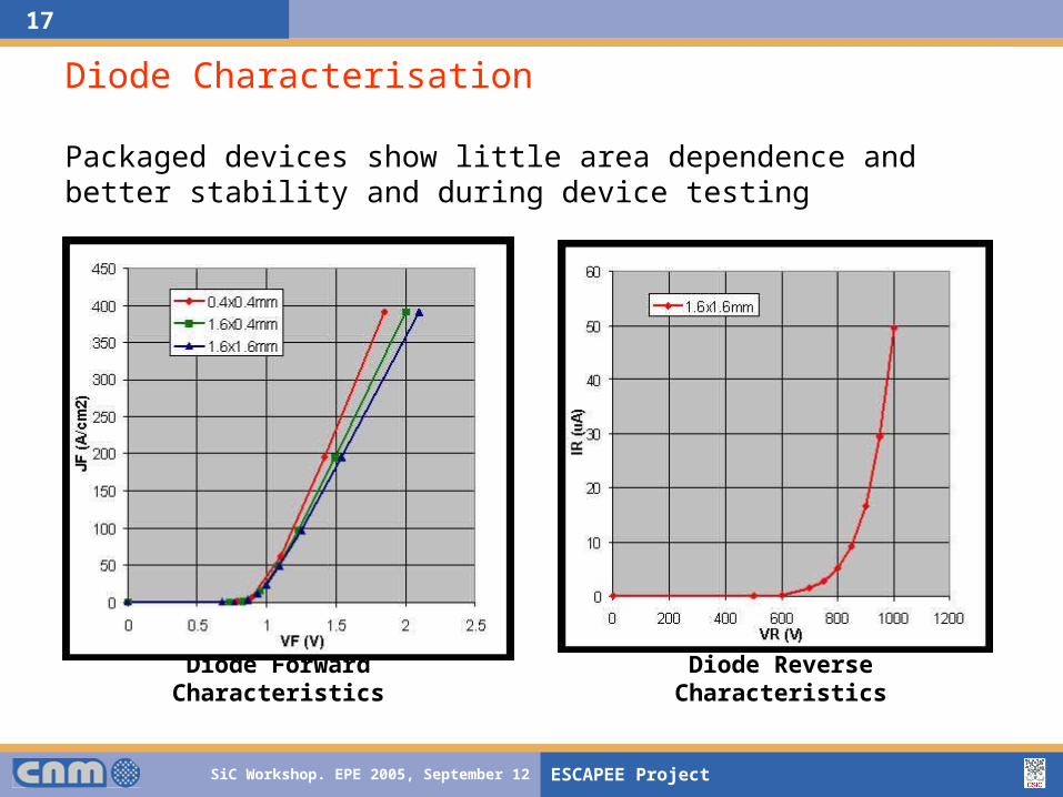
Diode Characterisation
Packaged devices show little area dependence and better stability and during device testing
Diode Forward Characteristics Diode Reverse Characteristics
SiC Workshop. EPE 2005, September 12 ESCAPEE Project
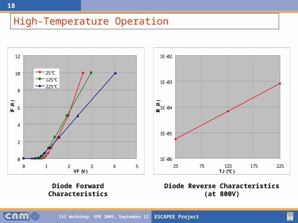
18
High-Temperature Operation
0
2
4
6
8
10
12
0 1 2 3 4 5VF (V)
IF (
A)
25°C
125°C
225°C
1E-06
1E-05
1E-04
1E-03
1E-02
25 75 125 175 225TJ (°C)
IR (
A)
Diode Reverse Characteristics (at 800V)Diode Forward Characteristics
SiC Workshop. EPE 2005, September 12 ESCAPEE Project
19
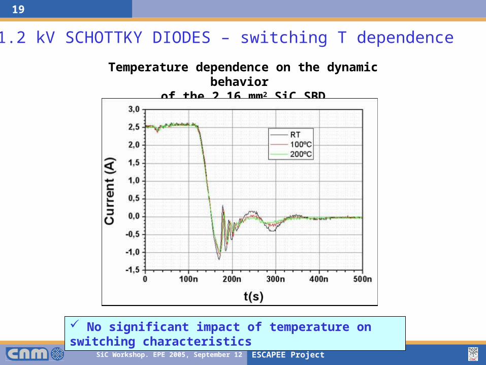
Temperature dependence on the dynamic behavior
of the 2.16 mm2 SiC SBD
1.2 kV SCHOTTKY DIODES – switching T dependence
No significant impact of temperature on switching characteristics
SiC Workshop. EPE 2005, September 12 ESCAPEE Project
20
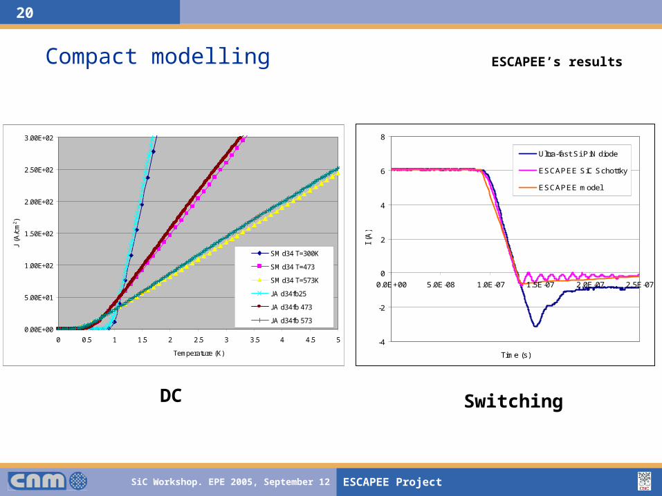
ESCAPEE’s resultsCompact modelling
-4
-2
0
2
4
6
8
0.0E+00 5.0E-08 1.0E-07 1.5E-07 2.0E-07 2.5E-07
Time (s)
I (A
)
Ultra-fast Si PiN diode
ESCAPEE SiC Schottky
ESCAPEE model
0.00E+00
5.00E+01
1.00E+02
1.50E+02
2.00E+02
2.50E+02
3.00E+02
0 0.5 1 1.5 2 2.5 3 3.5 4 4.5 5
Temperature (K)
J (A
/cm
2)
SM d34 T=300K
SM d34 T=473
SM d34 T=573K
JA d34fb25
JA d34fb 473
JA d34fb 573
DC Switching

SiC Workshop. EPE 2005, September 12 ESCAPEE Project
21
1.2KV Hybrid Module
• Aerospace IGBT/diode half-bridge module.
• 150A 1200V Infineon Silicon IGBT.
• Four 1.6x1.6mm 1000V ESCAPEE SiC Schottky Diodes in parallel.
• AlSiC Baseplate, Al/AlN substrate, Cu lead-frame, PBT ring-frame and lid.
• PbSnAg solder and vacuum furnace die-attach.
• 5mil/12 mil Al wire-bonds. Si IGBT/SiC diode hybridmodule with lid removed
SiC Workshop. EPE 2005, September 12 ESCAPEE Project
22
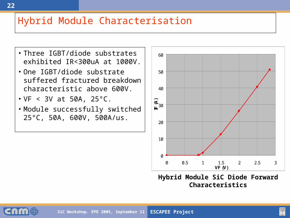
Hybrid Module Characterisation
• Three IGBT/diode substrates exhibited IR<300uA at 1000V.
• One IGBT/diode substrate suffered fractured breakdown characteristic above 600V.
• VF < 3V at 50A, 25°C.• Module successfully switched
25°C, 50A, 600V, 500A/us.
0
10
20
30
40
50
60
0 0.5 1 1.5 2 2.5 3VF (V)
IF (
A)
Hybrid Module SiC Diode Forward Characteristics
SiC Workshop. EPE 2005, September 12 ESCAPEE Project
23
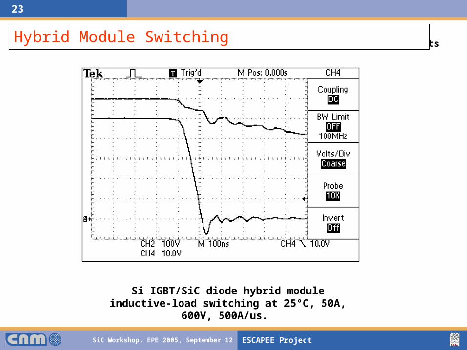
ESCAPEE’s results
Si IGBT/SiC diode hybrid module inductive-load switching at 25°C, 50A, 600V, 500A/us.
Hybrid Module Switching
SiC Workshop. EPE 2005, September 12 ESCAPEE Project
24
3.5 kV SCHOTTKY DIODES
SiC Workshop. EPE 2005, September 12 ESCAPEE Project
25
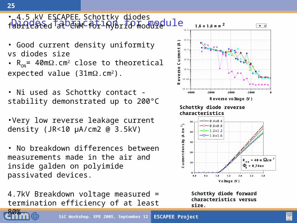
Diodes fabrication for module• 4.5 kV ESCAPEE Schottky diodes fabricated at CNM for hybrid module
• Good current density uniformity vs diodes size• RON= 40m.cm2 close to theoretical expected
value (31m.cm2).
• Ni used as Schottky contact - stability demonstrated up to 200°C
•Very low reverse leakage current density (JR<10 µA/cm2 @ 3.5kV)
• No breakdown differences between measurements made in the air and inside galden on polyimide passivated devices.
4.7kV Breakdown voltage measured = termination efficiency of at least 80%
0,0 0,5 1,0 1,5 2,0 2,5 3,00
10
20
30
40
50
RON
= 40 m.cm2
B = 0,74ev C
urr
ent
den
sity
(A
/cm
2 )Voltage (V)
0.4x0.4 0.8x0.8 1.2x1.2 1.6x1.6
Schottky diode forward characteristics versus size.
-4000 -3000 -2000 -1000 01E-11
1E-10
1E-9
1E-8
1E-7
1E-6
1E-5
1,6 x 1,6 mm2
Rev
erse
Cu
rren
t (A
)
Reverse voltage (V)
Id
Schottky diode reverse characteristics
SiC Workshop. EPE 2005, September 12 ESCAPEE Project
26
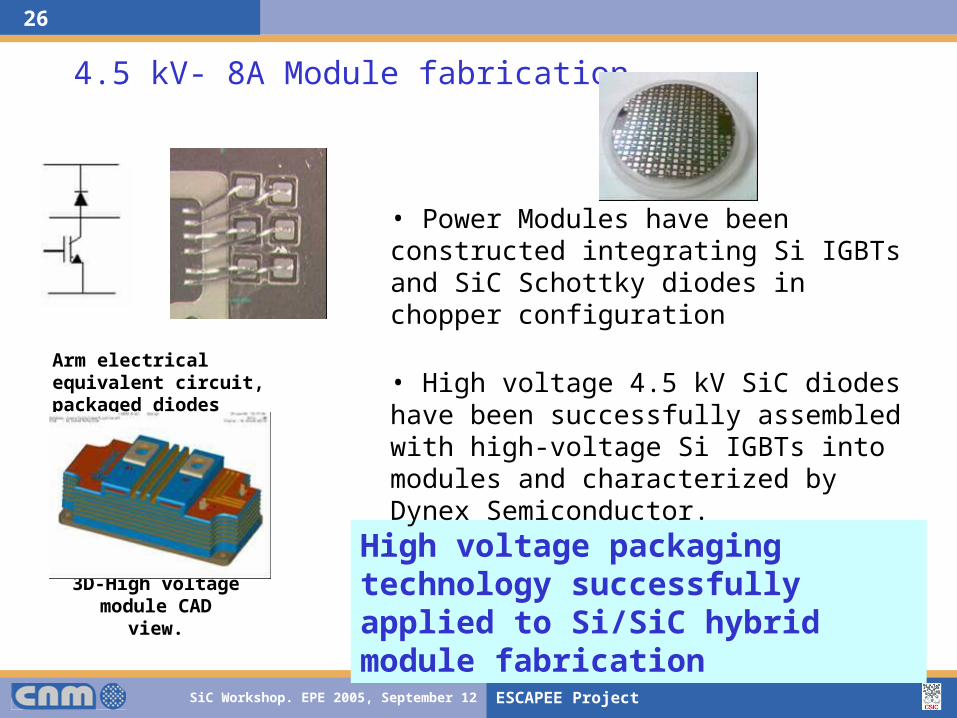
4.5 kV- 8A Module fabrication
High voltage packaging technology successfully applied to Si/SiC hybrid module fabrication
• Power Modules have been constructed integrating Si IGBTs and SiC Schottky diodes in chopper configuration
• High voltage 4.5 kV SiC diodes have been successfully assembled with high-voltage Si IGBTs into modules and characterized by Dynex Semiconductor.
3D-High voltage module CAD
view.
Arm electrical equivalent circuit, packaged diodes
SiC Workshop. EPE 2005, September 12 ESCAPEE Project
27
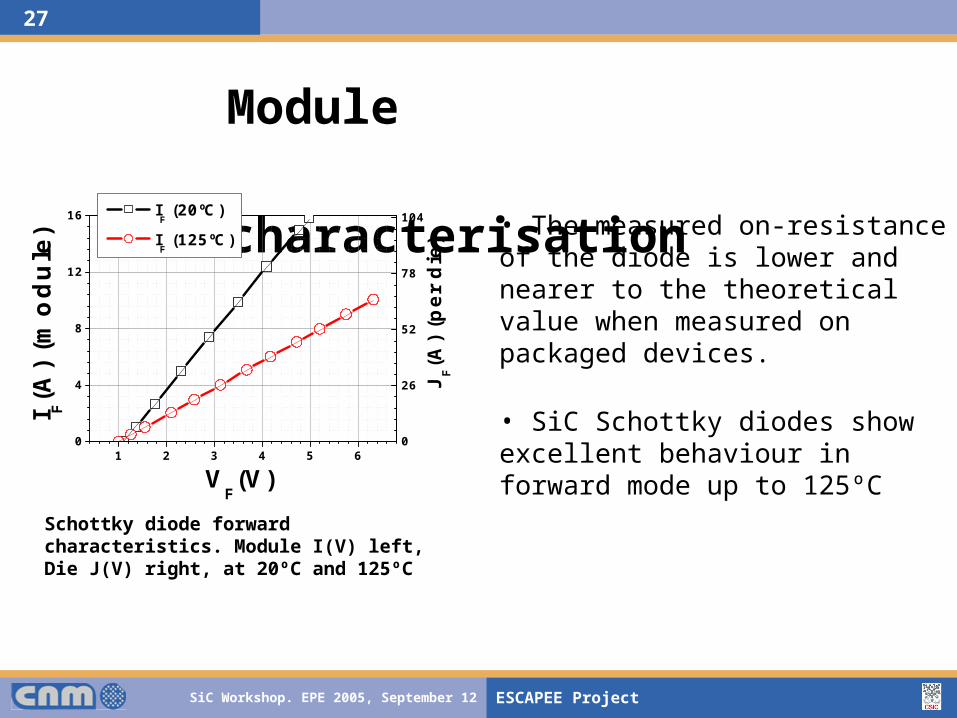
Module
characterisation• The measured on-resistance of the diode is lower and nearer to the theoretical value when measured on packaged devices.
• SiC Schottky diodes show excellent behaviour in forward mode up to 125ºC
1 2 3 4 5 60
4
8
12
16
0
26
52
78
104
JF(A
) (p
er
die
)
I F(A
) (m
od
ule
)
VF(V)
IF (20ºC)
IF (125ºC)
Schottky diode forward characteristics. Module I(V) left, Die J(V) right, at 20ºC and 125ºC
SiC Workshop. EPE 2005, September 12 ESCAPEE Project
28
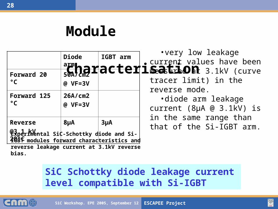
Module
characterisation
SiC Schottky diode leakage current level compatible with Si-IGBT
•very low leakage current values have been measured at 3.1kV (curve tracer limit) in the reverse mode.
•diode arm leakage current (8µA @ 3.1kV) is in the same range than that of the Si-IGBT arm.
Experimental SiC-Schottky diode and Si-IGBT modules forward characteristics and reverse leakage current at 3.1kV reverse bias.
Diode arm
IGBT arm
Forward 20 °C
50A/cm2 @ VF=3V
Forward 125 °C
26A/cm2 @ VF=3V
Reverse @3.1 kV, 20°C
8µA 3µA
SiC Workshop. EPE 2005, September 12 ESCAPEE Project
29
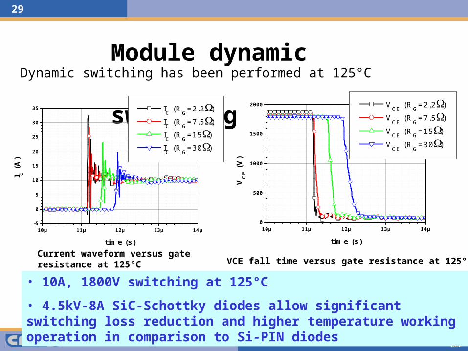
Module dynamic
switching
Dynamic switching has been performed at 125°C
10µ 11µ 12µ 13µ 14µ-5
0
5
10
15
20
25
30
35
I C (
A)
time (s)
IC (RG=2.2)
IC (RG=7.5)
IC (RG=15)
IC (RG=30)
10µ 11µ 12µ 13µ 14µ0
500
1000
1500
2000
VC
E (
V)
time (s)
VCE (RG=2.2)
VCE (RG=7.5)
VCE (RG=15)
VCE (RG=30)
Current waveform versus gate resistance at 125°C (VCE=1.8kV)
VCE fall time versus gate resistance at 125°C
• 10A, 1800V switching at 125°C
• 4.5kV-8A SiC-Schottky diodes allow significant switching loss reduction and higher temperature working operation in comparison to Si-PIN diodes
SiC Workshop. EPE 2005, September 12 ESCAPEE Project
30
Power MOSFET Fabrication
SiC Workshop. EPE 2005, September 12 ESCAPEE Project
31
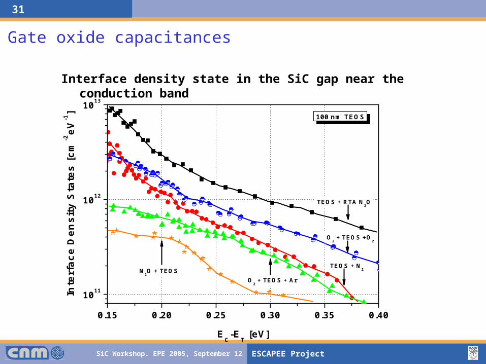
Interface density state in the SiC gap near the conduction band
Gate oxide capacitances
0.15 0.20 0.25 0.30 0.35 0.40
1011
1012
1013
TEOS + RTA N2O
TEOS + N2
O2 + TEOS +O
2
O2 + TEOS + Ar
100 nm TEOS
Inte
rfac
e D
ensi
ty S
tate
s [c
m-2eV
-1]
EC-E
T [eV]
N2O + TEOS

SiC Workshop. EPE 2005, September 12 ESCAPEE Project
32
Lateral N-MOSFET test structure
N-MOSFET on 4H-SiC: Thermal N2O /100nm TEOS / 950ºC O2
• Current higher than usual (x4 compared to LiU S230) • Threshold voltage: in the range –1V / 0.5V ( short/long channel)• Channel mobility: 40- 45 cm2/Vs (on epilayer layer annealed at 1600ºC) • Stable up to 15V
0 1 2 3 4 50,0
0,5
1,0
1,5
Vg=2V
Vg=4V
Vg=6V
Vg=8V
Dra
in C
urr
ent
[mA
]
Drain-Source Bias [V]
Vg=10V
-4 -2 0 2 4 6 8 10 12 140
10
20
30
40
50
60
Thermal Oxide
Eff
ecti
ve M
ob
ilit
y ef
f [cm
2 /Vs]
Gate Bias [V]
N2O + TEOS
Channel mobility vs gate bias
SiC Workshop. EPE 2005, September 12 ESCAPEE Project
33
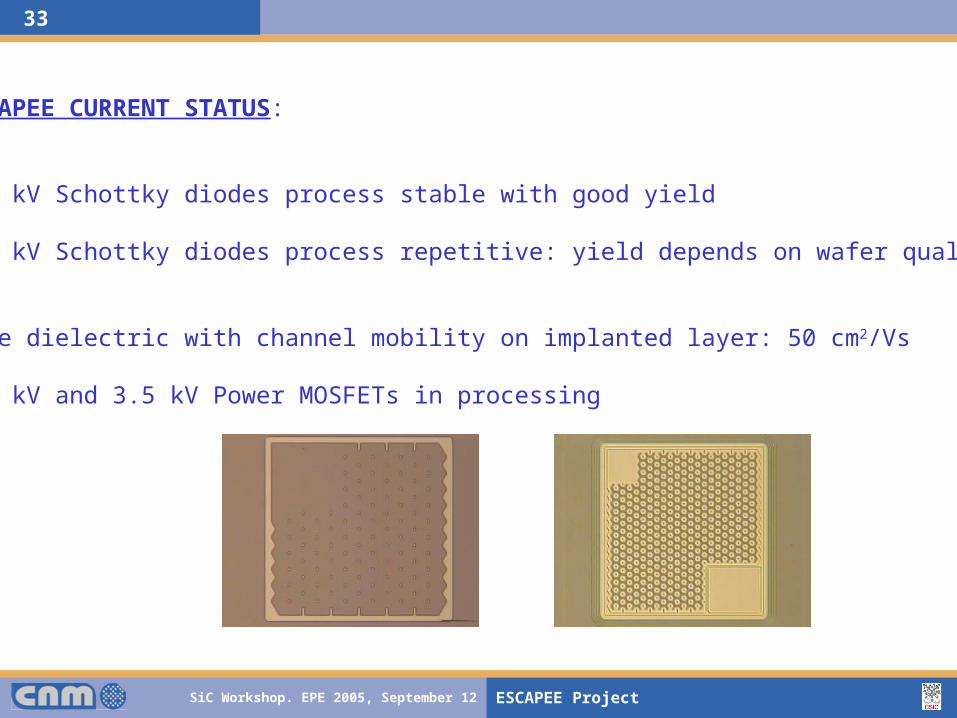
ESCAPEE CURRENT STATUS:
1.2 kV Schottky diodes process stable with good yield
3.5 kV Schottky diodes process repetitive: yield depends on wafer quality
Gate dielectric with channel mobility on implanted layer: 50 cm2/Vs
1.2 kV and 3.5 kV Power MOSFETs in processing
SiC Workshop. EPE 2005, September 12 ESCAPEE Project
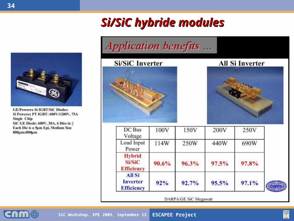
34
Si/SiC hybride modulesSi/SiC hybride modules