Si860x Data Sheet - silabs.com · isolator channel creating a stable latched low condition on both...
40
Si860x Data Sheet Bidirectional I 2 C Isolators with Unidirectional Digital Channels The Si860x series of isolators are single-package galvanic isolation solutions for I 2 C and SMBus serial port applications. These products are based on Silicon Labs proprietary RF isolation technology and offer shorter propagation delays, lower power consumption, smaller installed size, and more stable operation with temperature and age versus opto couplers or other digital isolators. All devices in this family include hot-swap, bidirectional SDA and/or SCL isolation chan- nels with open-drain, 35 mA sink capability that operate to a maximum frequency of 1.7 MHz. The 8-pin version (Si8600) supports bidirectional SDA and SCL isolation; the Si8602 supports bidirectional SDA and unidirectional SCL isolation, and the 16-pin ver- sions (Si8605, Si8606) feature two unidirectional isolation channels to support additional system signals, such as interrupts or resets. All versions contain protection circuits to guard against data errors when an unpowered device is inserted into a powered system. Small size, low installed cost, low power consumption, and short propagation delays make the Si860x family the optimum solution for isolating I 2 C and SMBus serial ports. Automotive Grade is available for certain part numbers. These products are built using automotive-specific flows at all steps in the manufacturing process to ensure the robust- ness and low defectivity required for automotive applications. KEY FEATURES • Independent, bidirectional SDA and SCL isolation channels • Open drain outputs with 35 mA sink current • Supports I 2 C clocks up to 1.7 MHz • Unidirectional isolation channels support additional system signals (Si8605, Si8606) • Up to 5000 VRMS isolation • UL, CSA, VDE, CQC recognition • 60-year life at rated working voltage • High electromagnetic immunity • Wide operating supply voltage • 3.0 to 5.5 V • Wide temperature range • –40 to +125 °C • Transient immunity 50 kV/µs • AEC-Q100 qualification • RoHS-compliant packages • SOIC-8 narrow body • SOIC-16 wide body • SOIC-16 narrow body • RoHS-compliant packages • SOIC-16 wide body • SOIC-16 narrow body • SOIC-8 narrow body • Automotive-grade OPNs available • AIAG compliant PPAP documentation support • IMDS and CAMDS listing support Industrial Applications • Isolated I 2 C, SMBus • Power over Ethernet • Motor Control Systems • Hot-swap applications • Intelligent Power systems Safety Regulatory Approvals • UL 1577 recognized • Up to 5000 V RMS for 1 minute • CSA component notice 5A approval • IEC 60950-1, 61010-1, 60601-1 (re- inforced insulation) • VDE certification conformity • Si863xxT options certified to rein- forced VDE 0884-10 • All other options certified to IEC 60747-5-5 and reinforced 60950-1 • CQC certification approval • GB4943.1 Automotive Applications • On-board chargers • Battery management systems • Charging stations • Traction inverters • Hybrid Electric Vehicles • Battery Electric Vehicles silabs.com | Building a more connected world. Rev. 1.71 • Isolated digital power supply communications
Transcript of Si860x Data Sheet - silabs.com · isolator channel creating a stable latched low condition on both...

Si860x Data Sheet
Bidirectional I2C Isolators with Unidirectional Digital Channels
The Si860x series of isolators are single-package galvanic isolation solutions for I2C andSMBus serial port applications. These products are based on Silicon Labs proprietaryRF isolation technology and offer shorter propagation delays, lower power consumption,smaller installed size, and more stable operation with temperature and age versus optocouplers or other digital isolators.
All devices in this family include hot-swap, bidirectional SDA and/or SCL isolation chan-nels with open-drain, 35 mA sink capability that operate to a maximum frequency of 1.7MHz. The 8-pin version (Si8600) supports bidirectional SDA and SCL isolation; theSi8602 supports bidirectional SDA and unidirectional SCL isolation, and the 16-pin ver-sions (Si8605, Si8606) feature two unidirectional isolation channels to support additionalsystem signals, such as interrupts or resets. All versions contain protection circuits toguard against data errors when an unpowered device is inserted into a powered system.
Small size, low installed cost, low power consumption, and short propagation delaysmake the Si860x family the optimum solution for isolating I2C and SMBus serial ports.
Automotive Grade is available for certain part numbers. These products are built usingautomotive-specific flows at all steps in the manufacturing process to ensure the robust-ness and low defectivity required for automotive applications.
KEY FEATURES
• Independent, bidirectional SDA and SCLisolation channels• Open drain outputs with 35 mA sink
current• Supports I2C clocks up to 1.7 MHz
• Unidirectional isolation channels supportadditional system signals (Si8605, Si8606)
• Up to 5000 VRMS isolation• UL, CSA, VDE, CQC recognition• 60-year life at rated working voltage• High electromagnetic immunity• Wide operating supply voltage
• 3.0 to 5.5 V• Wide temperature range
• –40 to +125 °C• Transient immunity 50 kV/µs• AEC-Q100 qualification• RoHS-compliant packages
• SOIC-8 narrow body• SOIC-16 wide body• SOIC-16 narrow body
• RoHS-compliant packages• SOIC-16 wide body• SOIC-16 narrow body• SOIC-8 narrow body
• Automotive-grade OPNs available• AIAG compliant PPAP documentation
support• IMDS and CAMDS listing support
Industrial Applications• Isolated I2C, SMBus
• Power over Ethernet• Motor Control Systems• Hot-swap applications• Intelligent Power systems
Safety Regulatory Approvals• UL 1577 recognized
• Up to 5000 VRMS for 1 minute• CSA component notice 5A approval
• IEC 60950-1, 61010-1, 60601-1 (re-inforced insulation)
• VDE certification conformity• Si863xxT options certified to rein-
forced VDE 0884-10• All other options certified to IEC
60747-5-5 and reinforced 60950-1• CQC certification approval
• GB4943.1
Automotive Applications• On-board chargers• Battery management systems• Charging stations• Traction inverters• Hybrid Electric Vehicles• Battery Electric Vehicles
silabs.com | Building a more connected world. Rev. 1.71
• Isolated digital power supply communications

1. Ordering Guide
Table 1.1. Ordering Guide1, 2
Ordering PartNumber (OPN)
Number of Bi-directional
I2C Channels
Max I2C BusSpeed (MHz)
Number ofUnidirection-
al Non-I2CChannels
Max DataRate of
Non-I2C Uni-directionalChannels
(Mbps)
IsolationRatings(kVrms)
Temp Range(°C)
Package
Si8600AB-B-IS 2 1.7 0 — 2.5 –40 to 125 NB SOIC-8
Si8600AC-B-IS 2 1.7 0 — 3.75 –40 to 125 NB SOIC-8
Si8600AD-B-IS 2 1.7 0 — 5.0 –40 to 125 WB SOIC-16
Si8602AB-B-IS 1 1.7 1 10 2.5 –40 to 125 NB SOIC-8
Si8602AC-B-IS 1 1.7 1 10 3.75 –40 to 125 NB SOIC-8
Si8602AD-B-IS 1 1.7 1 10 5.0 –40 to 125 WB SOIC-16
Si8605AB-B-IS1 2 1.7 1 Forward
1 Reverse
10 2.5 –40 to 125 NB SOIC-16
Si8605AC-B-IS1 2 1.7 1 Forward
1 Reverse
10 3.75 –40 to 125 NB SOIC-16
Si8605AD-B-IS 2 1.7 1 Forward
1 Reverse
10 5.0 –40 to 125 WB SOIC-16
Si8606AC-B-IS1 2 1.7 2 Forward 10 3.75 –40 to 125 NB SOIC-16
Si8606AD-B-IS 2 1.7 2 Forward 10 5.0 –40 to 125 WB SOIC-16
Note:1. All packages are RoHS-compliant with peak reflow temperature of 260 °C according to the JEDEC industry standard classifica-
tions and peak solder temperature.2. “Si” and “SI” are used interchangeably.3. An "R" at the end of the part number denotes tape and reel packaging option.
Si860x Data SheetOrdering Guide
silabs.com | Building a more connected world. Rev. 1.71 | 2

Automotive Grade OPNs
Automotive-grade devices are built using automotive-specific flows at all steps in the manufacturing process to ensure robustness andlow defectivity. These devices are supported with AIAG-compliant Production Part Approval Process (PPAP) documentation, and fea-ture International Material Data System (IMDS) and China Automotive Material Data System (CAMDS) listing. Qualifications are compli-ant with AEC-Q100, and a zero-defect methodology is maintained throughout definition, design, evaluation, qualification, and mass pro-duction steps.
Table 1.2. Ordering Guide for Automotive Grade OPNs1, 2, 4, 5
Ordering PartNumber (OPN)
Number ofBi- direction-al I2C Chan-
nels
Max I2C BusSpeed (MHz)
Number ofUnidirection-
al Non-I2CChannels
Max DataRate of Non-I2C Uni-direc-tional Chan-nels (Mbps)
Isolation Rat-ing (kV)
Temp Range(°C)
Package
Si8602AD-AS 1 1.7 1 10 5.0 –40 to 125 WB SOIC-16
Si8605AD-AS 2 1.7 1 Forward
1 Reverse
10 5.0 –40 to 125 WB SOIC-16
Si8606AD-AS 2 1.7 2 Forward 10 5.0 –40 to 125 WB SOIC-16
Note:1. All packages are RoHS-compliant with peak reflow temperatures of 260 °C according to the JEDEC industry standard classifica-
tions.2. “Si” and “SI” are used interchangeably.3. An "R" at the end of the part number denotes tape and reel packaging option.4. Automotive-Grade devices (with an "–A" suffix) are identical in construction materials, topside marking, and electrical parameters
to their Industrial-Grade (with a "–I" suffix) version counterparts. Automotive-Grade products are produced utilizing full automotiveprocess flows and additional statistical process controls throughout the manufacturing flow. The Automotive-Grade part number isincluded on shipping labels.
5. Additional Ordering Part Numbers may be available in Automotive-Grade. Please contact your local Silicon Labs sales represen-tative for further information.
Si860x Data SheetOrdering Guide
silabs.com | Building a more connected world. Rev. 1.71 | 3

Table of Contents1. Ordering Guide . . . . . . . . . . . . . . . . . . . . . . . . . . . . . . 2
2. System Overview . . . . . . . . . . . . . . . . . . . . . . . . . . . . . . 62.1 Theory of Operation . . . . . . . . . . . . . . . . . . . . . . . . . . . . 6
3. Typical Application Overview . . . . . . . . . . . . . . . . . . . . . . . . . 7
3.1 I2C Background . . . . . . . . . . . . . . . . . . . . . . . . . . . . . 7
3.2 I2C Isolator Operation . . . . . . . . . . . . . . . . . . . . . . . . . . . 7
3.3 I2C Isolator Design Constraints . . . . . . . . . . . . . . . . . . . . . . . . 8
3.4 I2C Isolator Design Considerations . . . . . . . . . . . . . . . . . . . . . . . 8
3.5 Typical Application Schematics . . . . . . . . . . . . . . . . . . . . . . . . 9
4. Device Operation . . . . . . . . . . . . . . . . . . . . . . . . . . . . . 114.1 Device Startup . . . . . . . . . . . . . . . . . . . . . . . . . . . . .11
4.2 Undervoltage Lockout . . . . . . . . . . . . . . . . . . . . . . . . . . .11
4.3 Input and Output Characteristics for Non-I2C Digital Channels . . . . . . . . . . . . .12
4.4 Layout Recommendations. . . . . . . . . . . . . . . . . . . . . . . . . .124.4.1 Supply Bypass . . . . . . . . . . . . . . . . . . . . . . . . . . .124.4.2 Output Pin Termination. . . . . . . . . . . . . . . . . . . . . . . . .12
4.5 Typical Performance Characteristics . . . . . . . . . . . . . . . . . . . . . .13
5. Electrical Specifications . . . . . . . . . . . . . . . . . . . . . . . . . . 145.1 Test Circuits . . . . . . . . . . . . . . . . . . . . . . . . . . . . . .19
6. Pin Descriptions . . . . . . . . . . . . . . . . . . . . . . . . . . . . . 246.1 Si8600/02 SOIC-8 Package . . . . . . . . . . . . . . . . . . . . . . . . .24
6.2 Si8600/02 SOIC-16 Package . . . . . . . . . . . . . . . . . . . . . . . . .25
6.3 Si8605/06 SOIC-16 Package . . . . . . . . . . . . . . . . . . . . . . . . .26
7. Package Outline: 16-Pin Wide Body SOIC. . . . . . . . . . . . . . . . . . . . 27
8. Land Pattern: 16-Pin Wide-Body SOIC . . . . . . . . . . . . . . . . . . . . . 29
9. Package Outline: 8-Pin Narrow Body SOIC . . . . . . . . . . . . . . . . . . . 30
10. Land Pattern: 8-Pin Narrow Body SOIC . . . . . . . . . . . . . . . . . . . . 31
11. Package Outline: 16-Pin Narrow Body SOIC . . . . . . . . . . . . . . . . . . 32
12. Land Pattern: 16-Pin Narrow Body SOIC. . . . . . . . . . . . . . . . . . . . 34
13. Si860x Top Markings . . . . . . . . . . . . . . . . . . . . . . . . . . . 3513.1 Top Marking: 16-Pin Wide Body SOIC . . . . . . . . . . . . . . . . . . . . .35
13.2 Top Marking: 8-Pin Narrow Body SOIC . . . . . . . . . . . . . . . . . . . . .36
13.3 Top Marking: 16-Pin Narrow Body SOIC . . . . . . . . . . . . . . . . . . . .37
silabs.com | Building a more connected world. Rev. 1.71 | 4

14. Revision History. . . . . . . . . . . . . . . . . . . . . . . . . . . . . 38
silabs.com | Building a more connected world. Rev. 1.71 | 5

2. System Overview
2.1 Theory of Operation
The operation of an Si86xx channel is analogous to that of an opto coupler, except an RF carrier is modulated instead of light. Thissimple architecture provides a robust isolated data path and requires no special considerations or initialization at start-up. A simplifiedblock diagram for a single unidirectional Si86xx channel is shown in the figure below.
RF OSCILLATOR
MODULATOR DEMODULATORA BSemiconductor-Based Isolation
Barrier
Transmitter Receiver
Figure 2.1. Simplified Channel Diagram
A channel consists of an RF Transmitter and RF Receiver separated by a semiconductor-based isolation barrier. Referring to theTransmitter, input A modulates the carrier provided by an RF oscillator using on/off keying. The Receiver contains a demodulator thatdecodes the input state according to its RF energy content and applies the result to output B via the output driver. This RF on/off keyingscheme is superior to pulse code schemes as it provides best-in-class noise immunity, low power consumption, and better immunity tomagnetic fields. See the following figure for more details.
Input Signal
Output Signal
Modulation Signal
Figure 2.2. Modulation Scheme
Si860x Data SheetSystem Overview
silabs.com | Building a more connected world. Rev. 1.71 | 6

3. Typical Application Overview
3.1 I2C Background
In many applications, I2C, SMBus, and other digital power supply communications, including those for bus power management, the interfaces require galvanic isolation for safety or ground loop elimination. For example, Power over Ethernet (PoE) applications typically use an I2C interface for communication between the PoE power sourcing device (PSE), and the earth ground referenced system controller. Galvanic isolation is required both by standard and also as a practical matter to prevent ground loops in Ethernet connected equipment.
The physical interface consists of two wires: serial data (SDA) and serial clock (SCL). These wires are connected to open collectordrivers that serve as both inputs and outputs. At first glance, it appears that SDA and SCL can be isolated simply by placing two unidir-ectional isolators in parallel, and in opposite directions. However, this technique creates feedback that latches the bus line low when alogic low asserted by either master or slave. This problem can be remedied by adding anti-latch circuits, but results in a larger and moreexpensive solution. The Si860x products offer a single-chip, anti-latch solution to the problem of isolating I2C/SMBus applications andrequire no external components except the I2C/SMBus pull-up resistors. In addition, they provide isolation to a maximum of 5.0 kVRMS,support I2C clock stretching, and operate to a maximum I2C bus speed of 1.7 Mbps.
3.2 I2C Isolator Operation
Without anti-latch protection, bidirectional I2C isolators latch when an isolator output logic low propagates back through an adjacentisolator channel creating a stable latched low condition on both sides. Anti-latch protection is typically added to one side of the isolatorto avoid this condition (the “A” side for the Si8600/02/05/06).
The following examples illustrate typical circuit configurations using the Si8600/02/05/06.
I2C/SMBusUnit 1
Si8600/02/05/06
I2C/SMBusUnit 2
ISO1
ISO2
VOL
VIL
+-
VOL
VIL
A Si
de
B Si
de
Figure 3.1. Isolated Bus Overview (I2C Channels Only)
The “A side” output low (VOL) and input low (VIL) levels are designed such that the isolator VOL is greater than the isolator VIL to preventthe latch condition.
Si860x Data SheetTypical Application Overview
silabs.com | Building a more connected world. Rev. 1.71 | 7

3.3 I2C Isolator Design Constraints
The table below lists the I2C isolator design constraints.
Table 3.1. Design Constraints
Design Constraint Data Sheet Values Effect of Bus Pull-up Strengthand Temperature
To prevent the latch condition, theisolator output low level must begreater than the isolator input lowlevel.
Isolator VOL 0.7 V typical
Isolator VIL 0.5 V typical
Input/Output Logic Low LevelDifference
ΔVSDA1, ΔVSCL1 = 50 mV mini-mum
This is normally guaranteed by the isolator data sheet.However, if the pull up strength is too weak, the outputlow voltage will fall and can get too close to the input lowlogic level. These track over temperature.
The bus output low must be lessthan the isolator input low logic level.
Bus VOL = 0.4 V maximum
Isolator VIL = 0.41 V minimum
If the pull up strength is too large, the devices on thebus might not pull the voltage below the input low range.These have opposite temperature coefficients. Worstcase is hot temperature.
The isolator output low must be lessthan the bus input low.
Bus VIL 0.3 x VDD = 1.0 V minimumfor VDD = 3.3 V
Isolator VOL = 0.8 V maximum
If the pull up strength is too large, the isolator might notpull below the bus input low voltage.
Si8600/02/05/06 Vol: –1.8 mV/C
CMOS buffer: –0.6 mV/C
This provides some temperature tracking, but worstcase is cold temperature.
3.4 I2C Isolator Design Considerations
The first step in applying an I2C isolator is to choose which side of the bus will be connected to the isolator A side. Ideally, it should bethe side which:
Is compatible with the range of bus pull up specified by the manufacturer. For example, the Si8600/02/05/06 isolators are normally usedwith a pull up of 0.5 mA to 3 mA.
Has the highest input low level for devices on the bus. Some devices may specify an input low of 0.9 V and other devices might requirean input low of 0.3 x Vdd. Assuming a 3.3 V minimum power supply, the side with an input low of 0.3 x Vdd is the better side becausethis side has an input low level of 1.0 V.
Have devices on the bus that can pull down below the isolator input low level. For example, the Si860x input level is 0.41 V. As mostCMOS devices can pull to within 0.4 V of GND this is generally not an issue.
Has the lowest noise. Due to the special logic levels, noise margins can be as low as 50 mV.
Si860x Data SheetTypical Application Overview
silabs.com | Building a more connected world. Rev. 1.71 | 8

3.5 Typical Application Schematics
The figures below illustrate typical circuit configurations using the Si8600, Si8602, Si8605, and Si8606.
1
2 7
Si8600
3
8AVDD
ASDA
ASCL
AGND BGND
BSCL
BSDA
BVDD
3k 3k0.1 µF0.1 µF3k 3k
I2C Bus6
54
Figure 3.2. Typical Si8600 Application Diagram
1
2 7
Si8602
3
8AVDD
ASDA
ASCL
AGND BGND
BSCL
BSDA
BVDD
3k0.1 µF0.1 µF3k
I2C Bus6
54
Figure 3.3. Typical Si8602 Application Diagram
1
2
3
4
5
6
7
15
14
13
12
11
10
8 9Si8600
3
16
AVDD
ASDA
ASCL
AGNDBGND
BSCL
BSDA
BVDD
3k 3k0.1 µF0.1 µF
3k 3kI2C Bus
AGND BGND
Figure 3.4. Typical Si8600 Application Diagram
Si860x Data SheetTypical Application Overview
silabs.com | Building a more connected world. Rev. 1.71 | 9

1
2
3
4
5
6
7
15
14
13
12
11
10
8 9Si8602
3
16
AVDD
ASDA
ASCL
AGND
BGND
BSCL
BSDA
BVDD
3k0.1 µF0.1 µF
3kI2C Bus
AGND BGND
Figure 3.5. Typical Si8602 Application Diagram
1
2
3
4
5
6
7
15
14
13
12
11
10
8 9Si8605
3
16AVDD
ASDA
ASCL
AGND
Micro-controller
Micro-controller
BGND
BSCL
BSDA
BVDD
3k 3k0.1 µF0.1 µF
3k 3k
I2C BusRESET
INT
Figure 3.6. Typical Si8605 Application Diagram
1
2
3
4
5
6
7
15
14
13
12
11
10
8 9Si8606
3
16AVDD
ASDA
ASCL
AGND
Micro-controller
BGND
BSCL
BSDA
BVDD
3k 3k0.1 µF0.1 µF
3k 3k
I2C Bus
RESET
INT
Figure 3.7. Typical Si8606 Application Diagram
Si860x Data SheetTypical Application Overview
silabs.com | Building a more connected world. Rev. 1.71 | 10

4. Device Operation
Device behavior during start-up, normal operation, and shutdown is shown in Figure 4.1 Device Behavior during Normal Operation onpage 11, where UVLO+ and UVLO- are the positive-going and negative-going thresholds respectively. Refer to Table 4.1 Si86xx Op-eration Table on page 12 to determine outputs when power supply (VDD) is not present.
4.1 Device Startup
Outputs are held low during powerup until VDD is above the UVLO threshold for time period tSTART. Following this, the outputs followthe states of inputs.
4.2 Undervoltage Lockout
Undervoltage Lockout (UVLO) is provided to prevent erroneous operation during device startup and shutdown or when VDD is below itsspecified operating circuits range. Both Side A and Side B each have their own undervoltage lockout monitors. Each side can enter orexit UVLO independently. For example, Side A unconditionally enters UVLO when AVDD falls below AVDDUVLO– and exits UVLO whenAVDD rises above AVDDUVLO+. Side B operates the same as Side A with respect to its BVDD supply.
INPUT
AVDD
UVLO-
BVDD
UVLO+
UVLO-UVLO+
OUTPUT
tSTART tSTART tSTARTtPHL tPLHtSD
Figure 4.1. Device Behavior during Normal Operation
Si860x Data SheetDevice Operation
silabs.com | Building a more connected world. Rev. 1.71 | 11

4.3 Input and Output Characteristics for Non-I2C Digital Channels
The unidirectional Si86xx inputs and outputs are standard CMOS drivers/receivers. The nominal output impedance of an isolator driverchannel is approximately 50 Ω, ±40%, which is a combination of the value of the on-chip series termination resistor and channel resist-ance of the output driver FET. When driving loads where transmission line effects will be a factor, output pins should be appropriatelyterminated with controlled impedance PCB traces. Table 4.1 Si86xx Operation Table on page 12 details powered and unpoweredoperation of the Si86xx’s non-I2C digital channels.
Table 4.1. Si86xx Operation Table
VI Input1, 4 VDDI State11,2,3 VDDO State1,2,3 VO Output1, 4 Comments
H P P H Normal operation.
L P P L
X UP P L Upon transition of VDDI from un-powered to powered, VO returns tothe same state as VI in less than 1µs.
X P UP Undetermined Upon transition of VDDO from un-powered to powered, VO returns tothe same state as VI within 1 µs.
Note:
1. VDDI and VDDO are the input and output power supplies. VI and VO are the respective input and output terminals.2. Powered (P) state is defined as 3.0 V < VDD < 5.5 V.3. Unpowered (UP) state is defined as VDD = 0 V.4. X = not applicable; H = Logic High; L = Logic Low.5. Note that an I/O can power the die for a given side through an internal diode if its source has adequate current.6. For I2C channels, the outputs for a given side go to Hi-Z when power is lost on the opposite side.
4.4 Layout Recommendations
To ensure safety in the end user application, high voltage circuits (i.e., circuits with >30 VAC) must be physically separated from thesafety extra-low voltage circuits (SELV is a circuit with <30 VAC) by a certain distance (creepage/clearance). If a component, such as adigital isolator, straddles this isolation barrier, it must meet those creepage/clearance requirements and also provide a sufficiently largehigh-voltage breakdown protection rating (commonly referred to as working voltage protection). Table 5.6 Regulatory Information1 onpage 19 and Table 5.7 Insulation and Safety-Related Specifications on page 20 detail the working voltage and creepage/clearancecapabilities of the Si86xx. These tables also detail the component standards (UL1577, IEC60747, CSA 5A), which are readily acceptedby certification bodies to provide proof for end-system specifications requirements. Refer to the end-system specification (61010-1,60950-1, 60601-1, etc.) requirements before starting any design that uses a digital isolator.
4.4.1 Supply Bypass
The Si860x family requires a 0.1 µF bypass capacitor between AVDD and AGND and BVDD and BGND. The capacitor should beplaced as close as possible to the package. To enhance the robustness of a design, the user may also include resistors (50–300 Ω ) inseries with the inputs and outputs if the system is excessively noisy.
4.4.2 Output Pin Termination
The nominal output impedance of an non-I2C isolator channel is approximately 50 Ω, ±40%, which is a combination of the value of theon-chip series termination resistor and channel resistance of the output driver FET. When driving loads where transmission line effectswill be a factor, output pins should be appropriately terminated with controlled impedance PCB traces.
Si860x Data SheetDevice Operation
silabs.com | Building a more connected world. Rev. 1.71 | 12

4.5 Typical Performance Characteristics
The typical performance characteristics depicted in the following diagrams are for information purposes only. Refer to Tables Table5.2 Si860x Power Characteristics1 on page 14, Table 5.3 Si8600/02/05/06 Electrical Characteristics for Bidirectional I2C Channels1 onpage 15, Table 5.4 Electrical Characteristics for Unidirectional Non-I2C Digital Channels (Si8602/05/06) on page 17, and Table5.5 Electrical Characteristics for All I2C and Non-I2C Channels on page 18 for actual specification limits.
Figure 4.2. I2C Side A Pulling Down(1100 Ω Pull-Up)
Figure 4.3. I2C Side A Pulling Up, Side B Following
Figure 4.4. I2C Side B Pulling Down
Figure 4.5. Non I2C Channel Propagation Delay vs. Temperature
Figure 4.6. I2C Side B Pulling Up, Side A Following
Si860x Data SheetDevice Operation
silabs.com | Building a more connected world. Rev. 1.71 | 13

5. Electrical Specifications
Table 5.1. Recommended Operating Conditions
Parameter Symbol Min Typ Max Unit
Ambient Operating Temperature1 TA –40 25 125* °C
Supply VoltageAVDD 3.0 — 5.5 V
BVDD 3.0 — 5.5 V
Note:1. The maximum ambient temperature is dependent on data frequency, output loading, number of operating channels, and supply
voltage.
Table 5.2. Si860x Power Characteristics1
3.0 V < VDD < 5.5 V. TA = –40 to +125 °C. Typical specs at 25 °C (See Figure 5.2 Simplified Timing Test Diagram on page 19 andFigure 3.2 Typical Si8600 Application Diagram on page 9 for test diagrams.)
Parameter Symbol Test Condition Min Typ Max Unit
Si8600 Supply Current
AVDD Current
BVDD Current
Idda
IddbAll channels = 0 dc
—
—
5.4
4.3
7.6
6.5
mA
mA
AVDD Current
BVDD Current
Idda
IddbAll channels = 1 dc
—
—
2.6
1.9
3.9
2.9
mA
mA
AVDD Current
BVDD Current
Idda
IddbAll channels = 1.7 MHz
—
—
3.3
2.6
5.0
3.9
mA
mA
Si8602 Supply Current
AVDD Current
BVDD Current
Idda
IddbAll channels = 0 dc
—
—
1.8
1.8
2.7
2.7
mA
mA
AVDD Current
BVDD Current
Idda
IddbAll channels = 1 dc
—
—
4.7
3.1
7.1
4.7
mA
mA
AVDD Current
BVDD Current
Idda
IddbAll channels = 1.7 MHz
—
—
2.5
2.1
3.8
3.2
mA
mA
Si8605 Supply Current
AVDD Current
BVDD Current
Idda
Iddb
All non-I2C channels = 0
All I2C channels = 1
—
—
3.4
2.7
5.1
4.1
mA
mA
AVDD Current
BVDD Current
Idda
Iddb
All non-I2C channels = 1
All I2C channels = 0
—
—
7.2
6.2
10.1
8.7
mA
mA
AVDD Current
BVDD Current
Idda
Iddb
All non-I2C channels = 5 MHz
All I2C channels = 1.7 MHz
—
—
4.2
3.6
6.3
5.4
mA
mA
Si860x Data SheetElectrical Specifications
silabs.com | Building a more connected world. Rev. 1.71 | 14
Parameter Symbol Test Condition Min Typ Max Unit
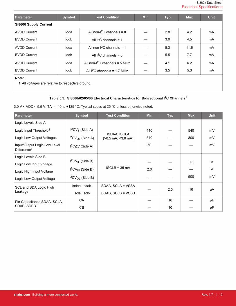
Si8606 Supply Current
AVDD Current
BVDD Current
Idda
Iddb
All non-I2C channels = 0
All I2C channels = 1
—
—
2.8
3.0
4.2
4.5
mA
mA
AVDD Current
BVDD Current
Idda
Iddb
All non-I2C channels = 1
All I2C channels = 0
—
—
8.3
5.5
11.6
7.7
mA
mA
AVDD Current
BVDD Current
Idda
Iddb
All non-I2C channels = 5 MHz
All I2C channels = 1.7 MHz
—
—
4.1
3.5
6.2
5.3
mA
mA
Note:1. All voltages are relative to respective ground.
Table 5.3. Si8600/02/05/06 Electrical Characteristics for Bidirectional I2C Channels1
3.0 V < VDD < 5.5 V. TA = –40 to +125 °C. Typical specs at 25 °C unless otherwise noted.
Parameter Symbol Test Condition Min Typ Max Unit
Logic Levels Side A
Logic Input Threshold2
Logic Low Output Voltages
Input/Output Logic Low LevelDifference3
I2CVT (Side A)
I2CVOL (Side A)
I2CΔV (Side A)
ISDAA, ISCLA(>0.5 mA, <3.0 mA)
410
540
50
—
—
—
540
800
—
mV
mV
mV
Logic Levels Side B
Logic Low Input Voltage
Logic High Input Voltage
Logic Low Output Voltage
I2CVIL (Side B)
I2CVIH (Side B)
I2CVOL (Side B)
ISCLB = 35 mA—
2.0
—
—
—
—
0.8
—
500
V
V
mV
SCL and SDA Logic HighLeakage
Isdaa, Isdab
Iscla, Isclb
SDAA, SCLA = VSSA
SDAB, SCLB = VSSB— 2.0 10 µA
Pin Capacitance SDAA, SCLA,SDAB, SDBB
CA
CB
—
—
10
10
—
—
pF
pF
Si860x Data SheetElectrical Specifications
silabs.com | Building a more connected world. Rev. 1.71 | 15

Parameter Symbol Test Condition Min Typ Max Unit
Timing Specifications (Measured at 1.40 V Unless Otherwise Specified)
Maximum I2C Bus Frequency Fmax — — 1.7 MHz
Propagation Delay
5 V Operation
Side A to Side B Rising 4
Side A to Side B Falling 4
Side B to Side A Rising
Side B to Side A Falling
3.3 V Operation
Side A to Side B Rising 4
Side A to Side B Falling 4
Side B to Side A Rising
Side B to Side A Falling
Tphab
Tplab
Tphba
Tplba
Tphab
Tplab
Tphba
Tplba
No bus capacitance,
R1 = 1400
R2 = 499
See Figure 5.2 SimplifiedTiming Test Diagram on
page 19
R1 = 806
R2 = 499
—
—
—
—
—
—
—
—
38
15
33
11
44
17
30
14
45
26
46
22
55
29
40
27
ns
ns
ns
ns
ns
ns
ns
ns
Pulse Width Distortion
5 V
Side A Low to Side B Low 4
Side B Low to Side A Low
3.3 V
Side A Low to Side B Low 4
Side B Low to Side A Low
PWDAB
PWDBA
PWDAB
PWDBA
No bus capacitance
R1 = 1400
R2 = 499
See Figure 5.2 SimplifiedTiming Test Diagram on
page 19
R1 = 806
R2 = 499
—
—
—
—
22
21
27
15
32
32
35
25
ns
ns
ns
ns
Note:
1. All voltages are relative to respective ground.2. VIL < 0.410 V, VIH > 0.540 V.
3. I2CΔV (Side A) = I2CVOL (Side A) – I2CVT (Side A). To ensure no latch-up on a given bus, I2CΔV (Side A) is the minimum differ-ence between the output logic low level of the driving device and the input logic threshold.
4. Side A measured at 0.6 V.
Si860x Data SheetElectrical Specifications
silabs.com | Building a more connected world. Rev. 1.71 | 16

Table 5.4. Electrical Characteristics for Unidirectional Non-I2C Digital Channels (Si8602/05/06)
3.0 V < VDD < 5.5 V. TA = –40 to +125 °C. Typical specs at 25 °C
Parameter Symbol Test Condition Min Typ Max Unit
Positive-Going Input Threshold VT+ All inputs rising 1.4 1.67 1.9 V
Negative-Going Input Threshold VT– All inputs falling 1.0 1.23 1.4 V
Input Hysteresis VHYS 0.38 0.44 0.50 V
High Level Input Voltage VIH 2.0 — — V
Low Level Input Voltage VIL — — 0.8 V
High Level Output Voltage VOH loh = –4 mAAVDD,BVDD –0.4
4.8 — V
Low Level Output Voltage VOL lol = 4 mA — 0.2 0.4 V
Input Leakage Current IL — — ±10 µA
Output Impedance1 ZO — 50 — Ω
Timing Characteristics
Maximum Data Rate 0 — 10 Mbps
Minimum Pulse Width — — 40 ns
Propagation Delay tPHL, tPLHSee Figure 5.1 Propagation Delay Timing
(Non-I2C Channels) on page 18— — 20 ns
Pulse Width Distortion|tPLH – tPHL| PWD
See Figure 5.1 Propagation Delay Timing(Non-I2C Channels) on page 18
— — 12 ns
Propagation Delay Skew2 tPSK(P-P) — — 20 ns
Channel-Channel Skew tPSK — — 10 ns
Output Rise Time tr
C3 = 15 pF
See Figure 5.1 Propagation Delay Timing(Non-I2C Channels) on page 18 and Figure5.2 Simplified Timing Test Diagram on page
19
— 2.5 4.0 ns
Output Fall Time tf
C3 = 15 pF
See Figure 5.1 Propagation Delay Timing(Non-I2C Channels) on page 18 and Figure5.2 Simplified Timing Test Diagram on page
19
— 2.5 4.0 ns
Peak Eye Diagram Jitter tJIT(PK) — 350 — ps
Note:
1. The nominal output impedance of a non-I2C isolator driver channel is approximately 50 Ω, ±40%, which is a combination of thevalue of the on-chip series termination resistor and channel resistance of the output driver FET. When driving loads where trans-mission line effects will be a factor, output pins should be appropriately terminated with controlled impedance PCB traces.
2. tPSK(P-P) is the magnitude of the difference in propagation delay times measured between different units operating at the samesupply voltages, load, and ambient temperature.
Si860x Data SheetElectrical Specifications
silabs.com | Building a more connected world. Rev. 1.71 | 17

Table 5.5. Electrical Characteristics for All I2C and Non-I2C Channels
3.0 V < VDD < 5.5 V. TA = –40 to +125 °C. Typical specs at 25 °C
Parameter Symbol Test Condition Min Typ Max Unit
VDD Undervoltage Threshold VDDUV+ VDD1, VDD2 rising 1.95 2.24 2.375 V
VDD Undervoltage Threshold VDDUV– VDD1, VDD2 falling 1.88 2.16 2.325 V
VDD Undervoltage Hysteresis VDDHYS 50 70 95 mV
Common Mode TransientImmunity CMTI
VI = VDD or 0 V
VCM = 1500 V (see Figure5.3 Common Mode Transi-ent Immunity Test Circuit
on page 19)
35 50 — kV/µs
Shut Down Time from UVLO tSD — 3.0 — µs
Start-up Time1 tSTART — 15 40 µs
Note:1. Start-up time is the time period from the application of power to valid data at the output.
Typical Input
tPLH tPHL
Typical Output
tr tf
90%
10%
90%
10%1.4 V
1.4 V
Figure 5.1. Propagation Delay Timing (Non-I2C Channels)
Si860x Data SheetElectrical Specifications
silabs.com | Building a more connected world. Rev. 1.71 | 18

5.1 Test Circuits
Figure 5.2 Simplified Timing Test Diagram on page 19 depicts the timing test diagram; Figure 5.3 Common Mode Transient ImmunityTest Circuit on page 19 depicts the CMTI test diagram.
AVDD
NC
BVDD
NC
NC NC
ADOUT BDIN
ASDA BSDA
ASCL BSCL
ADIN BDOUT
AGND BGNDSi8605
C1 C1 C3
R1 R1R2R2
C3 C2 C2
Figure 5.2. Simplified Timing Test Diagram
Oscilloscope
3 to 5 VIsolated Supply
Si86xxBVDD
OUTPUT
3 to 5 VSupply
High Voltage Surge Generator
Vcm SurgeOutput
High Voltage Differential
Probe
BGNDAGND
AVDD
INPUTInput SignalSwitch
InputOutput
Isolated Ground
Figure 5.3. Common Mode Transient Immunity Test Circuit
Table 5.6. Regulatory Information1
CSA
The Si860x is certified under CSA Component Acceptance Notice 5A. For more details, see File 232873.
61010-1: Up to 600 VRMS reinforced insulation working voltage; up to 600 VRMS basic insulation working voltage.
60950-1: Up to 600 VRMS reinforced insulation working voltage; up to 1000 VRMS basic insulation working voltage.
60601-1: Up to 125 VRMS reinforced insulation working voltage; up to 380 VRMS basic insulation working voltage.
VDE
The Si860x is certified according to IEC 60747-5-2. For more details, see File 5006301-4880-0001.
Si860x Data SheetElectrical Specifications
silabs.com | Building a more connected world. Rev. 1.71 | 19

60747-5-2: Up to 1200 Vpeak for basic insulation working voltage.
60950-1: Up to 600 VRMS reinforced insulation working voltage; up to 1000 VRMS basic insulation working voltage.
UL
The Si860x is certified under UL1577 component recognition program. For more details, see File E257455.
Rated up to 5000 VRMS isolation voltage for basic protection.
CQC
The Si860x is certified under GB4943.1-2011. For more details, see certificates CQC13001096110 and CQC13001096239.
Rated up to 600 VRMS reinforced insulation working voltage; up to 1000 VRMS basic insulation working voltage.
Note:1. Regulatory Certifications apply to 2.5 kVRMS rated devices which are production tested to 3.0 kVRMS for 1 sec.
Regulatory Certifications apply to 3.75 kVRMS rated devices which are production tested to 4.5 kVRMS for 1 sec.Regulatory Certifications apply to 5.0 kVRMS rated devices which are production tested to 6.0 kVRMS for 1 sec.For more information, see 1. Ordering Guide.
Table 5.7. Insulation and Safety-Related Specifications
Parameter Symbol Test Condition Value Unit
NB SOIC-8
NBSOIC-16
WB SOIC-16
Nominal Air Gap (Clearance) L(1O1) 4.9 4.9 8.0 mm
Nominal External Tracking (Creepage)1 L(1O2) 4.01 4.01 8.0 mm
Minimum Internal Gap
(Internal Clearance)
0.014 0.014 0.014 mm
Tracking Resistance(Proof Tracking Index)
PTI IEC60112 600 600 600 VRMS
Erosion Depth ED 0.040 0.019 0.019 mm
Resistance (Input-Output)2 RIO 1012 1012 1012 Ω
Capacitance (Input-Output)2 CIO f = 1 ΜΗz 1.0 2.0 2.0 pF
Input Capacitance3 CI Νon−Ι2C Channel 4.0 4.0 4.0 pF
I2C Channel 10 10 10 pF
Note:
1. VDE certifies the clearance and creepage limits as 4.7 mm minimum for the NB SOIC-8 and SOIC-16 packages and 8.5 mmminimum for the WB SOIC-16 package. UL does not impose a clearance and creepage minimum for component level certifica-tions. CSA certifies the clearance and creepage limits as 3.9 mm minimum for the NB SOIC-8 and SOIC-16 packages and 7.6mm minimum for the WB SOIC-16 package.
2. To determine resistance and capacitance, the Si860x, SO-16, is converted into a 2-terminal device. Pins 1–8 (1–4, SO-8) areshorted together to form the first terminal and pins 9–16 (5–8, SO-8) are shorted together to form the second terminal. The pa-rameters are then measured between these two terminals.
3. Measured from input pin to ground.
Si860x Data SheetElectrical Specifications
silabs.com | Building a more connected world. Rev. 1.71 | 20

Table 5.8. IEC 60664-1 (VDE 0844 Part 2) Ratings
Parameter Test Conditions Specification
NB SOIC-8SOIC-16
WB SOIC-16
Basic Isolation Group Material Group I I
Installation Classification Rated Mains Voltages < 150 VRMS I-IV I-IV
Rated Mains Voltages < 300 VRMS I-III I-IV
Rated Mains Voltages < 400 VRMS I-II I-III
Rated Mains Voltages < 600 VRMS I-II I-III
Table 5.9. IEC 60747-5-2 Insulation Characteristics for Si86xxxx1
Parameter Symbol Test Condition Characteristic Unit
WBSOIC-16
NB SOIC-8SOIC-16
Maximum Working Insulation Voltage VIORM 1200 630 Vpeak
Input to Output Test Voltage VPR Method b1(VIORM x 1.875 = VPR, 100%Production Test, tm = 1 sec,Partial Discharge < 5 pC)
2250 1182 Vpeak
Transient Overvoltage VIOTM t = 60 sec 6000 6000 Vpeak
Pollution Degree (DIN VDE 0110, Table 1)
2 2
Insulation Resistance at TS, VIO = 500 V RS >109 >109 Ω
Note:1. Maintenance of the safety data is ensured by protective circuits. The Si86xxxx provides a climate classification of 40/125/21.
Table 5.10. IEC Safety Limiting Values1
Parameter Symbol Test Condition NB SOIC-8 NB SOIC-16 WB SO-IC-16
Unit
Case Temperature TS 150 150 150 °C
Safety Input Current ΙS θJA = 100 °C/W (WB SOIC-16),105 °C/W (NB SOIC-16), 140
°C/W (NB SOIC-8)AVDD, BVDD = 5.5 V, TJ = 150
°C,
TA = 25 °C
160 210 220 mA
Device Power Dissipation2 PD 220 275 275 mW
Si860x Data SheetElectrical Specifications
silabs.com | Building a more connected world. Rev. 1.71 | 21

Parameter Symbol Test Condition NB SOIC-8 NB SOIC-16 WB SO-IC-16
Unit
Note:
1. Maximum value allowed in the event of a failure. Refer to the thermal derating curve in the three figures below.2. The Si86xx is tested with AVDD, BVDD = 5.5 V; TJ = 150 ºC; C1, C2 = 0.1 µF; C3 = 15 pF; R1, R2 = 3 kΩ; input 1 MHz 50% duty
cycle square wave.
Table 5.11. Thermal Characteristics
Parameter Symbol NB SOIC-8 NB SOIC-16 WB SOIC-16 Unit
IC Junction-to-Air Thermal Resistance θJA 140 105 100 °C/W
0 20015010050
400
200
100
0
Case Temperature (ºC)
Safe
ty-L
imiti
ng V
alue
s (m
A)
300
AVDD, BVDD = 3.6 V
AVDD, BVDD = 5.5 V
270
160
Figure 5.4. NB SOIC-8 Thermal Derating Curve, Dependence of Safety Limiting Values with Case Temperature per DIN EN 60747-5-2
0 20015010050
500
400
200
100
0
Temperature (ºC)
Safe
ty-L
imiti
ng C
urre
nt (m
A)
300
350
210AVDD , BVDD = 3.6 V
AVDD , BVDD = 5.5 V
Figure 5.5. NB SOIC-16 Thermal Derating Curve, Dependence of Safety Limiting Values with Case Temperature per DIN EN 60747-5-2
Si860x Data SheetElectrical Specifications
silabs.com | Building a more connected world. Rev. 1.71 | 22

0 20015010050
500
400
200
100
0
Temperature (ºC)
Safe
ty-L
imiti
ng C
urre
nt (m
A)
300
350
220AVDD , BVDD = 3.6 V
AVDD , BVDD = 5.5 V
Figure 5.6. WB SOIC-16 Thermal Derating Curve, Dependence of Safety Limiting Values with Case Temperature per DIN EN 60747-5-2
Table 5.12. Absolute Maximum Ratings1
Parameter Symbol Min Max Unit
Storage Temperature 2 TSTG –65 150 ºC
Ambient Temperature Under Bias TA –40 125 ºC
Junction Temperature TJ — 150 °C
Supply Voltage VDD –0.5 7.0 V
Input Voltage VI –0.5 VDD + 0.5 V
Output Voltage VO –0.5 VDD + 0.5 V
Output Current Drive (non-I2C channels) IO — ±10 mA
Side A output current drive (I2C channels) IO — ±15 mA
Side B output current drive (I2C channels) IO — ±75 mA
Lead Solder Temperature (10 s) — 260 ºC
Maximum Isolation (Input to Output) (1 sec)NB SOIC-8, SOIC-16
— 4500 VRMS
Maximum Isolation (Input to Output) (1 sec) WB SOIC-16
— 6500 VRMS
Note:
1. Permanent device damage may occur if the absolute maximum ratings are exceeded. Functional operation should be restricted toconditions as specified in the operational sections of this data sheet.
2. VDE certifies storage temperature from –40 to 150 °C.
Si860x Data SheetElectrical Specifications
silabs.com | Building a more connected world. Rev. 1.71 | 23

6. Pin Descriptions
6.1 Si8600/02 SOIC-8 Package
Bidirectional Isolator Channel
Bidirectional Isolator Channel
ASDA BSDA
ASCL BSCL
AGND BGND
AVDD BVDD
Si8600
1
2
3
4
8
7
6
5
Bidirectional Isolator Channel
Unidirectional Isolator Channel
ASDA BSDA
ASCL BSCL
AGND BGND
AVDD BVDD
Si8602
1
2
3
4
8
7
6
5
Table 6.1. Si8600/02 in SOIC-8 Package
Pin Name Description
1 AVDD Side A power supply terminal; connect to a source of 3.0to 5.5 V.
2 ASDA Side A data (open drain) input or output.
3 ASCL Side A clock input or output.
Open drain I/O for Si8600. Standard CMOS input forSi8602.
4 AGND Side A ground terminal.
5 BGND Side B ground terminal.
6 BSCL Side B clock input or output.
Open drain I/O for Si8600. Push-pull output for Si8602.
7 BSDA Side B data (open drain) input or output.
8 BVDD Side B power supply terminal; connect to a source of 3.0to 5.5 V.
Si860x Data SheetPin Descriptions
silabs.com | Building a more connected world. Rev. 1.71 | 24

6.2 Si8600/02 SOIC-16 Package
Bidirectional Isolator Channel
AVDD
NC
BVDD
NC
NC NC
ASDA BSDA
ASCL BSCL
Si8600
AGND
BGND
Bidirectional Isolator Channel
1
2
3
4
5
6
7
8
10
9
11
12
13
14
15
16
NC
AGND
BGND
NC
Bidirectional Isolator Channel
AVDD
NC
BVDD
NC
NC NC
ASDA BSDA
ASCL BSCL
Si8602
AGND
BGND
1
2
3
4
5
6
7
8
10
9
11
12
13
14
15
16
NC
AGND
BGND
UnidirectionalIsolator Channel
NC
Table 6.2. Si8600/02 in Narrow and Wide-Body SOIC-16 Packages
Pin Name Description
1 AGND Side A Ground Terminal.
2 NC No connection.
3 AVDD Side A power supply terminal. Connect to a source of3.0 to 5.5 V.
4 NC No connection.
5 ASDA Side A data open drain input or output.
6 ASCL Side A data open drain input or output.
7 AGND Side A Ground Terminal.
8 NC No connection.
9 BGND Side B Ground Terminal.
10 NC No connection.
11 BSCL Side B data open drain input or output.
12 BSDA Side B data open drain input or output.
13 NC No connection.
14 BVDD Side B power supply terminal. Connect to a source of3.0 to 5.5 V.
15 NC No connection.
16 BGND Side B Ground Terminal.
Si860x Data SheetPin Descriptions
silabs.com | Building a more connected world. Rev. 1.71 | 25

6.3 Si8605/06 SOIC-16 Package
Bidirectional Isolator Channel
AVDD
NC
BVDD
NC
NC NC
ADOUT BDIN
ASDA BSDAUnidirectional
Isolator Channel
ASCL BSCL
ADIN BDOUT
Si8605AGND BGND
UnidirectionalIsolator Channel
Bidirectional Isolator Channel
1
2
3
4
5
6
7
8
10
9
11
12
13
14
15
16
Bidirectional Isolator Channel
AVDD
NC
BVDD
NC
NC NC
ADIN2 BDOUT2
ASDA BSDAUnidirectional
Isolator Channel
ASCL BSCL
ADIN1 BDOUT1
Si8606AGND BGND
UnidirectionalIsolator Channel
Bidirectional Isolator Channel
1
2
3
4
5
6
7
8
10
9
11
12
13
14
15
16
Table 6.3. Si8605/06 in Narrow and Wide-Body SOIC-16 Packages
Pin Name Description
1 AVDD Side A power supply terminal. Connect to a source of3.0 to 5.5 V.
2 NC No connection.
3 ASDA Side A data (open drain) input or output.
4 ADIN/ADIN1 Side A standard CMOS digital input (non I2C).
5 ADOUT/ADIN2 Side A digital input/output (non I2C)
Standard CMOS digital input for Si8606.
Push-Pull output for Si8605.
6 ASCL Side A clock input or output.
Open drain I/O for Si8605/06.
7 NC No connection.
8 AGND Side A Ground Terminal.
9 BGND Side B Ground Terminal.
10 NC No connection.
11 BSCL Side B clock input or output.
Open drain I/O for Si8605/06.
12 BDIN/BDOUT2 Side B digital input/output (non I2C)
Standard CMOS digital input for Si8605.
Push-Pull output for Si8606.
13 BDOUT/BDOUT1 Side B digital push-pull output (non I2C).
14 BSDA Side B data open drain input or output.
15 NC No connection.
16 BVDD Side B power supply terminal. Connect to a source of3.0 to 5.5 V.
Si860x Data SheetPin Descriptions
silabs.com | Building a more connected world. Rev. 1.71 | 26

7. Package Outline: 16-Pin Wide Body SOIC
Figure 7.1 16-Pin Wide Body SOIC on page 27 illustrates the package details for the Si860x Digital Isolator. Table 7.1 Package Dia-gram Dimensions on page 27 lists the values for the dimensions shown in the illustration.
Figure 7.1. 16-Pin Wide Body SOIC
Table 7.1. Package Diagram Dimensions
Dimension Min Max
A — 2.65
A1 0.10 0.30
A2 2.05 —
b 0.31 0.51
c 0.20 0.33
D 10.30 BSC
E 10.30 BSC
E1 7.50 BSC
e 1.27 BSC
L 0.40 1.27
h 0.25 0.75
θ 0° 8°
aaa — 0.10
bbb — 0.33
ccc — 0.10
ddd — 0.25
eee — 0.10
fff — 0.20
Si860x Data SheetPackage Outline: 16-Pin Wide Body SOIC
silabs.com | Building a more connected world. Rev. 1.71 | 27

Dimension Min Max
Note:
1. All dimensions shown are in millimeters (mm) unless otherwise noted.2. Dimensioning and Tolerancing per ANSI Y14.5M-1994.3. This drawing conforms to JEDEC Outline MS-013, Variation AA.4. Recommended reflow profile per JEDEC J-STD-020 specification for small body, lead-free components.
Si860x Data SheetPackage Outline: 16-Pin Wide Body SOIC
silabs.com | Building a more connected world. Rev. 1.71 | 28

8. Land Pattern: 16-Pin Wide-Body SOIC
Figure 8.1 16-Pin SOIC Land Pattern on page 29 illustrates the recommended land pattern details for the Si860x in a 16-pin wide-body SOIC. Table 8.1 16-Pin Wide Body SOIC Land Pattern Dimensions on page 29 lists the values for the dimensions shown in theillustration.
Figure 8.1. 16-Pin SOIC Land Pattern
Table 8.1. 16-Pin Wide Body SOIC Land Pattern Dimensions
Dimension Feature (mm)
C1 Pad Column Spacing 9.40
E Pad Row Pitch 1.27
X1 Pad Width 0.60
Y1 Pad Length 1.90
Note:
1. This Land Pattern Design is based on IPC-7351 pattern SOIC127P1032X265-16AN for Density Level B (Median Land Protru-sion).
2. All feature sizes shown are at Maximum Material Condition (MMC) and a card fabrication tolerance of 0.05 mm is assumed.
Si860x Data SheetLand Pattern: 16-Pin Wide-Body SOIC
silabs.com | Building a more connected world. Rev. 1.71 | 29

9. Package Outline: 8-Pin Narrow Body SOIC
Figure 9.1 8-pin Small Outline Integrated Circuit (SOIC) Package on page 30 illustrates the package details for the Si860x in an 8-pinSOIC (SO-8). Table 9.1 Package Diagram Dimensions on page 30 lists the values for the dimensions shown in the illustration.
Figure 9.1. 8-pin Small Outline Integrated Circuit (SOIC) Package
Table 9.1. Package Diagram Dimensions
Symbol Millimeters
Min Max
A 1.35 1.75
A1 0.10 0.25
A2 1.40 REF 1.55 REF
B 0.33 0.51
C 0.19 0.25
D 4.80 5.00
E 3.80 4.00
e 1.27 BSC
H 5.80 6.20
h 0.25 0.50
L 0.40 1.27
� 0° 8°
Si860x Data SheetPackage Outline: 8-Pin Narrow Body SOIC
silabs.com | Building a more connected world. Rev. 1.71 | 30

10. Land Pattern: 8-Pin Narrow Body SOIC
Figure 10.1 PCB Land Pattern: 8-Pin Narrow Body SOIC on page 31 illustrates the recommended land pattern details for the Si860xin an 8-pin narrow-body SOIC. Table 10.1 PCM Land Pattern Dimensions (8-Pin Narrow Body SOIC) on page 31 lists the values forthe dimensions shown in the illustration.
Figure 10.1. PCB Land Pattern: 8-Pin Narrow Body SOIC
Table 10.1. PCM Land Pattern Dimensions (8-Pin Narrow Body SOIC)
Dimension Feature (mm)
C1 Pad Column Spacing 5.40
E Pad Row Pitch 1.27
X1 Pad Width 0.60
Y1 Pad Length 1.55
Note:
1. This Land Pattern Design is based on IPC-7351 pattern SOIC127P600X173-8N for Density Level B (Median Land Protrusion).2. All feature sizes shown are at Maximum Material Condition (MMC) and a card fabrication tolerance of 0.05 mm is assumed.
Si860x Data SheetLand Pattern: 8-Pin Narrow Body SOIC
silabs.com | Building a more connected world. Rev. 1.71 | 31

11. Package Outline: 16-Pin Narrow Body SOIC
Figure 11.1 16-pin Small Outline Integrated Circuit (SOIC) Package on page 32 illustrates the package details for the Si860x in a 16-pin narrow-body SOIC (SO-16). Table 11.1 Package Diagram Dimensions on page 32 lists the values for the dimensions shown inthe illustration.
Figure 11.1. 16-pin Small Outline Integrated Circuit (SOIC) Package
Table 11.1. Package Diagram Dimensions
Dimension Min Max
A — 1.75
A1 0.10 0.25
A2 1.25 —
b 0.31 0.51
c 0.17 0.25
D 9.90 BSC
E 6.00 BSC
E1 3.90 BSC
e 1.27 BSC
L 0.40 1.27
L2 0.25 BSC
h 0.25 0.50
θ 0° 8°
aaa 0.10
bbb 0.20
ccc 0.10
ddd 0.25
Si860x Data SheetPackage Outline: 16-Pin Narrow Body SOIC
silabs.com | Building a more connected world. Rev. 1.71 | 32

Dimension Min Max
Note:
1. All dimensions shown are in millimeters (mm) unless otherwise noted.2. Dimensioning and Tolerancing per ANSI Y14.5M-1994.3. This drawing conforms to the JEDEC Solid State Outline MS-012, Variation AC.4. Recommended card reflow profile is per the JEDEC/IPC J-STD-020 specification for Small Body Components.
Si860x Data SheetPackage Outline: 16-Pin Narrow Body SOIC
silabs.com | Building a more connected world. Rev. 1.71 | 33

12. Land Pattern: 16-Pin Narrow Body SOIC
Figure 12.1 16-Pin Narrow Body SOIC PCB Land Pattern on page 34 illustrates the recommended land pattern details for the Si860xin a 16-pin narrow-body SOIC. Table 12.1 16-Pin Narrow Body SOIC Land Pattern Dimensions on page 34 lists the values for thedimensions shown in the illustration.
Figure 12.1. 16-Pin Narrow Body SOIC PCB Land Pattern
Table 12.1. 16-Pin Narrow Body SOIC Land Pattern Dimensions
Dimension Feature (mm)
C1 Pad Column Spacing 5.40
E Pad Row Pitch 1.27
X1 Pad Width 0.60
Y1 Pad Length 1.55
Note:
1. This Land Pattern Design is based on IPC-7351 pattern SOIC127P600X165-16N for Density Level B (Median Land Protrusion).2. All feature sizes shown are at Maximum Material Condition (MMC) and a card fabrication tolerance of 0.05 mm is assumed.
Si860x Data SheetLand Pattern: 16-Pin Narrow Body SOIC
silabs.com | Building a more connected world. Rev. 1.71 | 34

13. Si860x Top Markings
13.1 Top Marking: 16-Pin Wide Body SOIC
Si86XYSVYYWWRTTTTT
CC e4
Figure 13.1. 16-Pin Wide Body SOIC Top Marking
Table 13.1. 16-Pin Wide Body SOIC Top Marking Explanation
Line 1 Marking: Base Part Number
Ordering Options
(See Ordering Guide for more in-formation).
Si86 = Isolator product series
XY = Channel Configuration
05 = Bidirectional SCL, SDA; 1- forward and 1-reverse unidirectional channel
06 = Bidirectional SCL, SDA; 2- forward unidirectional channels
S = Speed Grade
A = 1.7 Mbps
V = Isolation rating
A = 1 kV; B = 2.5 kV; C = 3.75 kV; D = 5.0 kV
Line 2 Marking: YY = Year
WW = Workweek
Assigned by assembly subcontractor. Corresponds to the yearand workweek of the mold date.
RTTTTT = Mfg Code Manufacturing code from assembly house
“R” indicates revision
Line 3 Marking: Circle = 1.7 mm Diameter
(Center-Justified)
“e4” Pb-Free Symbol
Country of Origin ISO Code Ab-breviation
CC = Country of Origin ISO Code Abbreviation• TW = Taiwan• TH = Thailand
Si860x Data SheetSi860x Top Markings
silabs.com | Building a more connected world. Rev. 1.71 | 35

13.2 Top Marking: 8-Pin Narrow Body SOIC
Si86XYSVYYWWRT
TTTT e3
Figure 13.2. 8-Pin Narrow Body SOIC Top Marking
Table 13.2. 8-Pin Narrow Body SOIC Top Marking Explanation
Line 1 Marking: Base Part Number
Ordering Options
(See Ordering Guide for more infor-mation).
Si86 = Isolator Product Series
XY = Channel Configuration
S = Speed Grade (max data rate)
V = Insulation rating
Line 2 Marking: YY = Year
WW = Work week
Assigned by assembly contractor. Corresponds to the yearand work week of the mold date.
R = Product Revision
T = First character of the manufac-turing code
First two characters of the manufacturing code from Assem-bly.
Line 3 Marking: Circle = 1.1 mm Diameter “e3” Pb-Free Symbol
TTTT = Last four characters of themanufacturing code
Last four characters of the manufacturing code from assem-bly.
Si860x Data SheetSi860x Top Markings
silabs.com | Building a more connected world. Rev. 1.71 | 36

13.3 Top Marking: 16-Pin Narrow Body SOIC
Si86XYSVYYWWRTTTTT e3
Figure 13.3. 16-Pin Narrow Body SOIC Top Marking
Table 13.3. 16-Pin Narrow Body SOIC Top Marking Explanation
Line 1 Marking: Base Part Number
Ordering Options
Si86 = Isolator product series
XY = Channel Configuration
05 = Bidirectional SCL, SDA; 1- forward and 1-reverse unidirectional channel
06 = Bidirectional SCL, SDA; 2- forward unidirectional channels
S = Speed Grade
A = 1.7 Mbps
V = Isolation rating
A = 1 kV; B = 2.5 kV; C = 3.75 kV
Line 2 Marking: Circle = 1.2 mm Diameter “e3” Pb-Free Symbol
YY = Year
WW = Work Week
Assigned by the Assembly House. Corresponds to the yearand work week of the mold date.
R = Product RevisionTTTTT = Mfg Code
Manufacturing code from assembly house
Si860x Data SheetSi860x Top Markings
silabs.com | Building a more connected world. Rev. 1.71 | 37

14. Revision History
Revision 1.71
January 2018• Added new table to Ordering Guide for Automotive-Grade OPN options.
Revision 1.7
April 18, 2017• Formatted tables in 5. Electrical Specifications.
Revision 1.6
February 2017• Corrected Figure 13.3.
Revision 1.5
July 2016• Converted data sheet to DITA.
Revision 1.4
• Updated Table 6.• Added CQC certificate numbers. Corrected Device Power Dissipation units in Table 10 on page 12.• Updated "Ordering Guide".• Removed references to moisture sensitivity levels.• Removed Note 2.
Revision 1.3
• Added Figure 3, “Common Mode Transient Immunity Test Circuit”.• Added references to CQC throughout.• Added references to 2.5 kVRMS devices throughout.• Removed Fail-safe operating mode throughout.• Updated "Ordering Guide".• Updated "Si860x Top Marking (16-Pin Wide Body SOIC)".
Revision 1.2• Updated Table 12.
• Added junction temperature spec.• Updated "Supply Bypass" .• Updated "Ordering Guide".
• Removed Rev A devices.• Updated "Package Outline: 16-Pin Wide Body SOIC".• Updated Top Marks.
• Added revision description.
Revision 1.1• Updated Figures 12 and 13.
• Updated Pin 7 AGND connection.• Updated "Ordering Guide" to include MSL2A.
Si860x Data SheetRevision History
silabs.com | Building a more connected world. Rev. 1.71 | 38

Revision 1.0• Reordered spec tables to conform to new convention.• Removed “pending” throughout document.
Revision 0.3
• Added chip graphics on page 1.• Moved Tables 1 and 2 to page 4.• Updated Table 7, “Insulation and Safety-Related Specifications”.• Updated Table 9, “IEC 60747-5-2 Insulation Characteristics for Si86xxxx*” .• Moved Table 13 to page 17.• Moved Table 14 to page 21.• Updated "Pin Descriptions" .• Updated "Ordering Guide" .
Revision 0.2
• Si8601 replaced by Si8602 throughout.• Added chip graphics.• Moved Table 12.• Updated Table 3, “Si8600/02/05/06 Electrical Characteristics for Bidirectional I2C Channels1”.• Updated Table 7, “Insulation and Safety-Related Specifications”.• Updated Table 9, “IEC 60747-5-2 Insulation Characteristics for Si86xxxx*,” on page 12.• Moved “3. Typical Application Overview” to page 16.• Moved “Typical Performance Characteristics” to page 23.• Updated "5.Pin Descriptions" on page 24.• Updated "6.Ordering Guide" on page 27.
Revision 0.1• Initial release.
Si860x Data SheetRevision History
silabs.com | Building a more connected world. Rev. 1.71 | 39

http://www.silabs.com
Silicon Laboratories Inc.400 West Cesar ChavezAustin, TX 78701USA
Smart. Connected. Energy-Friendly.
Productswww.silabs.com/products
Qualitywww.silabs.com/quality
Support and Communitycommunity.silabs.com
DisclaimerSilicon Labs intends to provide customers with the latest, accurate, and in-depth documentation of all peripherals and modules available for system and software implementers using or intending to use the Silicon Labs products. Characterization data, available modules and peripherals, memory sizes and memory addresses refer to each specific device, and "Typical" parameters provided can and do vary in different applications. Application examples described herein are for illustrative purposes only. Silicon Labs reserves the right to make changes without further notice and limitation to product information, specifications, and descriptions herein, and does not give warranties as to the accuracy or completeness of the included information. Silicon Labs shall have no liability for the consequences of use of the information supplied herein. This document does not imply or express copyright licenses granted hereunder to design or fabricate any integrated circuits. The products are not designed or authorized to be used within any Life Support System without the specific written consent of Silicon Labs. A "Life Support System" is any product or system intended to support or sustain life and/or health, which, if it fails, can be reasonably expected to result in significant personal injury or death. Silicon Labs products are not designed or authorized for military applications. Silicon Labs products shall under no circumstances be used in weapons of mass destruction including (but not limited to) nuclear, biological or chemical weapons, or missiles capable of delivering such weapons.
Trademark InformationSilicon Laboratories Inc.® , Silicon Laboratories®, Silicon Labs®, SiLabs® and the Silicon Labs logo®, Bluegiga®, Bluegiga Logo®, Clockbuilder®, CMEMS®, DSPLL®, EFM®, EFM32®, EFR, Ember®, Energy Micro, Energy Micro logo and combinations thereof, "the world’s most energy friendly microcontrollers", Ember®, EZLink®, EZRadio®, EZRadioPRO®, Gecko®, ISOmodem®, Micrium, Precision32®, ProSLIC®, Simplicity Studio®, SiPHY®, Telegesis, the Telegesis Logo®, USBXpress®, Zentri and others are trademarks or registered trademarks of Silicon Labs. ARM, CORTEX, Cortex-M3 and THUMB are trademarks or registered trademarks of ARM Holdings. Keil is a registered trademark of ARM Limited. All other products or brand names mentioned herein are trademarks of their respective holders.