SHREY SHARMA -...
71
Control and design of Quasi-Z-Source Inverter (qZSI) for grid connected Photovoltaic (PV) arrays Master’s thesis in Electric power engineering SHREY SHARMA Department of Electrical Engineering CHALMERS UNIVERSITY OF TECHNOLOGY Gothenburg, Sweden 2018
Transcript of SHREY SHARMA -...

Control and design of Quasi-Z-Source Inverter (qZSI) forgrid connected Photovoltaic (PV) arrays
Master’s thesis in Electric power engineering
SHREY SHARMA
Department of Electrical EngineeringCHALMERS UNIVERSITY OF TECHNOLOGYGothenburg, Sweden 2018


Master’s thesis 2018:NN
Control and design of Quasi-Z-Source Inverter(qZSI) for grid connected Photovoltaic (PV)
arrays
SHREY SHARMA
Department of Electrical EngineeringDivision of Electric power engineering
Chalmers University of TechnologyGothenburg, Sweden 2018

Control and design of Quasi-Z-Source Inverter (qZSI) for grid connected Photo-voltaic (PV) arrays
SHREY SHARMA
© SHREY SHARMA, 2018.
Supervisor & Examiner: Prof. YUJING LIU, Department of Electrical Engineering
Master’s Thesis 2018:NNDepartment of Electrical EngineeringDivision of Electric power engineeringChalmers University of TechnologySE-412 96 GothenburgTelephone +46 31 772 1000
Cover: Global irradiation (Wh/m2) on the 30th of May, 2013 obtained from SwedishMeteorological and Hydrological Institute (SMHI).
Typeset in LATEXGothenburg, Sweden 2018
iv
AbstractThe renewable energy sources are greener and more environment friendly than non-renewable energy sources. They are used for the sustainable power production. Solarenergy is abundant in a lot of places and can be tapped to satisfy energy needs. ThePhotovoltaic(PV) arrays can be connected to an inverter to convert DC output ofPV cells to AC supply for the grid. A type of converter that we can use for thisapplication is Quasi-Z-Source Inverter(qZSI). In this project, one of the task hasbeen to calculate and verify the value of elements used in the qZSI. The verificationwas done by pole-zero maps, bode plots and through optimization via simulationsof the model.This was followed by designing a controller for the DC side of the qZSI. Since itwas for DC side, it is called the DC side controller. Its design involved verificationof the transfer functions derived from the signal flow graph using Mason’s gain for-mula. The signal flow graph comes from the dynamic model of the qZSI. The blockdiagram from the transfer function was then simplified so as to apply the Internalmodel control(IMC) principle to obtain the proportional and integral constants(forthe inner and outer loop) of the controller. The inner loop is for the inductor cur-rent while the outer loop is for the DC link voltage. These were later fine-tuned toanother set of proportional and integral controller constants when both loops werecascaded.
Later, comparison of the output of qZSI’s Simulink model was done with the FroniusIG 15 inverter installed in Chalmers Grundkurs lab. It was also compared witha reference model*(already available in Simulink library which was optimized forcomparison with qZSI) which is Simulink model of a VSI connected with a boostconverter supplying the grid. The input for it is DC supply from PV arrays. Forcomparison it was important that the DC input remained same for both the models;the MPPT voltage input to VSI was sampled and used as input for qZSI model. Thefast fourier transform(FFT) and total harmonic distortion(THD) measurement ofthe output of all three inverters was compared. It was found that the Fronius inverterhad the least THD followed by VSI and then the qZSI. In all cases, THD was wellwithin the limit as per IEEE standard STD 519-2014. The FFT showed presence oflower odd harmonics in all three inverters. The magnitude of odd harmonics uponFFT followed the same suit as the THD.All in all, a much more fine tuned controller and better filters can be designed forthe qZSI to decrease the harmonics content. A better switching strategy can alsobe used to eliminate the harmonics. Considering that qZSI has a single stage unlikethe reference model* with cascaded boost and VSI inverter, it is cost effective touse qZSI plus it can perform both the buck and boost operations. This makes itan attractive replacement option of VSI for usage in applications like PV array andfuel cells.
Keywords: Photovoltaic(PV), Voltage source inverter(VSI), Harmonics, Impedance/Z-source inverter(ZSI), Quasi-impedance/Z-source inverter(qZSI), Shoot-through, To-tal Harmonic Distortion(THD), Pulse width modulation(PWM), Internal modelcontrol(IMC), Boost factor.
v


AcknowledgementsFirst of all, I would like to express my gratitude towards my examiner and super-visor Prof. Yujing Liu for being incredibly patient and supportive at all times andfor various technical inputs, ideas and encouragement I got from him.
I would also like to thank Prof Ola Carlson, Magnus Ellsen and Nima Saadat forthe discussions and help in data collection. I also appreciate Swedish Meteorologicaland Hydrological Institute (SMHI) and Curtis J Blank for their help in sourcingmore data.
Thanks to Junfei Tang, Ankit Gupta and Ehsan Behrouzian for all their help, avail-ability and technical discussions. I also appreciate and thank my fellow master’sstudents Nimananda Sharma, Shivadeep Maheshwar and Somadutta Sahoo for sup-port, suggestions and discussions. They made the thesis work a great experience.
Finally, I would like to express profound gratitude towards my family for theirconstant support and advice.
SHREY SHARMA, Gothenburg, Jan. 2018
vii


Contents
List of Figures xi
List of Tables xiii
1 Introduction 11.1 Aim . . . . . . . . . . . . . . . . . . . . . . . . . . . . . . . . . . . . 21.2 Sustainable development and ethical aspects . . . . . . . . . . . . . . 21.3 Scope . . . . . . . . . . . . . . . . . . . . . . . . . . . . . . . . . . . 31.4 Thesis structure . . . . . . . . . . . . . . . . . . . . . . . . . . . . . . 3
2 Photovoltaic array and inverters 52.1 Photovoltaic(PV) array . . . . . . . . . . . . . . . . . . . . . . . . . . 52.2 Converters . . . . . . . . . . . . . . . . . . . . . . . . . . . . . . . . 8
2.2.1 DC-DC converters . . . . . . . . . . . . . . . . . . . . . . . . 82.2.2 Inverters . . . . . . . . . . . . . . . . . . . . . . . . . . . . . . 92.2.3 The drawbacks and limitations of VSI and CSI . . . . . . . . . 10
2.3 Z-Source Inverter(ZSI) . . . . . . . . . . . . . . . . . . . . . . . . . . 112.4 Advantages and disadvantages of ZSI . . . . . . . . . . . . . . . . . . 132.5 Quasi-Z-Source Inverter(qZSI) . . . . . . . . . . . . . . . . . . . . . . 15
2.5.1 Circuit analysis of the Quasi-Z-Source Inverter(qZSI) . . . . . 152.6 Modeling of voltage fed Quasi-Z-Source Inverter(qZSI) . . . . . . . . 18
2.6.1 The steady state model of qZSI . . . . . . . . . . . . . . . . . 182.6.2 The small signal model of qZSI . . . . . . . . . . . . . . . . . 20
2.7 Type of control methods for shoot-through duty cycle . . . . . . . . 222.7.1 Closed loop control . . . . . . . . . . . . . . . . . . . . . . . . 22
2.7.1.1 Single control loop . . . . . . . . . . . . . . . . . . . 232.7.1.2 Double control loops . . . . . . . . . . . . . . . . . . 232.7.1.3 Other control methods . . . . . . . . . . . . . . . . . 24
3 Design of qZSI impedance network and controller 253.1 Designing qZSI impedance network . . . . . . . . . . . . . . . . . . . 253.2 Control strategy of qZSI . . . . . . . . . . . . . . . . . . . . . . . . . 29
3.2.1 Sinusoidal PWM and shoot-through implementation . . . . . . 293.3 DC side controller design for qZSI . . . . . . . . . . . . . . . . . . . . 32
3.3.1 Internal model control(IMC) . . . . . . . . . . . . . . . . . . . 323.3.2 Output saturation and anti-windup . . . . . . . . . . . . . . . 323.3.3 DC side controller . . . . . . . . . . . . . . . . . . . . . . . . . 33
ix

Contents
4 Results and Discussion 414.1 Results . . . . . . . . . . . . . . . . . . . . . . . . . . . . . . . . . . . 414.2 Sustainable development and ethical aspects . . . . . . . . . . . . . . 47
5 Future work and Conclusion 495.1 Future work . . . . . . . . . . . . . . . . . . . . . . . . . . . . . . . . 495.2 Conclusion . . . . . . . . . . . . . . . . . . . . . . . . . . . . . . . . . 50
Bibliography 51
A Appendix IA.1 IEEE Standard STD 519-2014 . . . . . . . . . . . . . . . . . . . . . . IA.2 Maximum power point tracking(MPPT) . . . . . . . . . . . . . . . . I
A.2.1 Incremental conductance . . . . . . . . . . . . . . . . . . . . . IIA.3 Matlab Script . . . . . . . . . . . . . . . . . . . . . . . . . . . . . . . III
A.3.1 Duty cycle function in controller subsystem . . . . . . . . . . III
x

List of Figures
1.1 Global irradiation (Wh/m2) on the 15th of March, 2017 obtained fromSwedish Meteorological and Hydrological Institute (SMHI)[1] . . . . 1
2.1 Single-diode equivalent circuit of a PV cell. . . . . . . . . . . . . . . . 52.2 The PV arrays at the southern side of Electric power engineering
building, Chalmers University, Johanneberg campus. Picture Cred-its[11] . . . . . . . . . . . . . . . . . . . . . . . . . . . . . . . . . . . 6
2.3 Fronius IG 15 inverter installed in Chalmers Grundkurs lab, Johan-neberg campus. . . . . . . . . . . . . . . . . . . . . . . . . . . . . . . 7
2.4 Simplified representation of grid connected PV array system at Chalmers. 82.5 Simple DC-DC boost converter circuit. . . . . . . . . . . . . . . . . . 82.6 Schematic diagram of a Voltage Source Inverter system. . . . . . . . . 92.7 Schematic diagram of a Current Source Inverter system. . . . . . . . 102.8 Schematic diagram of a Z-Source Inverter system. . . . . . . . . . . . 112.9 (a) Non shoot-through state equivalent circuit model of ZSI. (b)
Shoot-through state equivalent circuit model of ZSI. . . . . . . . . . . 122.10 (a)Voltage fed ZSI and (b) Voltage fed qZSI. . . . . . . . . . . . . . . 152.11 The qZSI equivalent circuit under (a) non-shoot-through and (b)
shoot-through state. . . . . . . . . . . . . . . . . . . . . . . . . . . . 162.12 Signal flow graph used to obtain transfer functions in equation 3.4
and 3.5 [18]. . . . . . . . . . . . . . . . . . . . . . . . . . . . . . . . . 212.13 PI controller used to control the qZSI shoot-through duty ratio. . . . 222.14 The various single loop controls for shoot-through duty ratio in qZSI. 232.15 The double loop control methods for shoot-through duty ratio in qZSI. 242.16 The non-linear control methods of shoot-through duty ratio in qZSI. . 24
3.1 Changes in poles and zeros upon varying inductance with constantC=300 µF . . . . . . . . . . . . . . . . . . . . . . . . . . . . . . . . . 26
3.2 Changes in poles upon varying capacitance with constant L=100 µH . 273.3 Bode plot for varying inductance and C=300 µF . . . . . . . . . . . . 283.4 Bode plot for varying capacitance and L=100 µH . . . . . . . . . . . 283.5 Implementation of a qZSI to grid connected PV arrays. . . . . . . . . 293.6 Sinusoidal PWM . . . . . . . . . . . . . . . . . . . . . . . . . . . . . 303.7 Sinusoidal PWM implementation in Simulink . . . . . . . . . . . . . . 313.8 Closed loop representation of plant model G(s) with controller trans-
fer function Fc(s). . . . . . . . . . . . . . . . . . . . . . . . . . . . . . 32
xi

List of Figures
3.9 The DC side controller design with PI controller in the inner loop . . 333.10 Simulink model of qZSI used to compare with the reference model* . 343.11 The reference model* available in Simulink library used for compari-
son with simulated qZSI model (power_PVarray_grid_det). . . . . . 353.12 Sampled MPPT voltage from the reference model* . . . . . . . . . . 363.13 Block diagram representation of the closed loop . . . . . . . . . . . . 363.14 Simplified block diagram representation of the closed loop . . . . . . 373.15 PI response to the inner control loop . . . . . . . . . . . . . . . . . . 383.16 PI response to the outer control loop . . . . . . . . . . . . . . . . . . 38
4.1 VP N voltage at qZSI . . . . . . . . . . . . . . . . . . . . . . . . . . . 414.2 Output voltage in phase ’a’ of simulated qZSI model . . . . . . . . . 424.3 Output current in phase ’a’ of simulated qZSI model . . . . . . . . . 424.4 Shoot-through duty cycle variation in simulated qZSI model . . . . . 434.5 Zoomed shoot-through duty cycle variation in simulated qZSI model . 434.6 FFT of output voltage of the installed inverter in Chalmers lab . . . . 444.7 FFT of VSI output voltage in reference model* . . . . . . . . . . . . 454.8 FFT of qZSI output voltage in phase ’a . . . . . . . . . . . . . . . . . 454.9 THD of VSI output voltage in phase ’a’ . . . . . . . . . . . . . . . . . 464.10 THD of qZSI output voltage in phase ’a’ . . . . . . . . . . . . . . . . 46
A.1 I-V and P-V characteristic plot of PV array used in simulation. . . . I
xii

List of Tables
2.1 The comparison of ZSI to CSI and VSI. . . . . . . . . . . . . . . . . . 14
3.1 Parameters used in Simulink qZSI model . . . . . . . . . . . . . . . . 293.2 PI controller parameters for separate inner and outer loop . . . . . . 373.3 PI controller parameters for cascaded inner and outer loop . . . . . . 39
xiii

List of Tables
xiv

1Introduction
Fuelled by the energy derived by fossil fuels the growth engine of the world had beenmoving pretty fast in the past century but with time people realized the effect ofpollution, coal mining and oil drilling on the environment. Currently sustainablegrowth can be realized with clean energy initiatives.With the rise in the quality oflife in countries around the world, the energy consumption is also increasing. Thismeans more loading on non-renewable energy sources. The solution of problem liesin turning to clean energy sources like solar, water, wind energy, etc.
Figure 1.1: Global irradiation (Wh/m2) on the 15th of March, 2017 obtained fromSwedish Meteorological and Hydrological Institute (SMHI)[1]
1

1. Introduction
The potential of solar energy is quite high not only in Sweden [2] but also in sun richplaces like China, India where the goal is to increase installed capacity to 100 GWby both the countries [3]. Other countries also have achievable goals for installedcapacity in solar energy segment [4].The decrease in cost and conducive government policies are a good impetus vital-izing the growth of solar energy sector. In recent years, tremendous increase in theinstalled capacity has been observed worldwide, especially concentrated in China,Japan and the USA followed by India, Germany, South Korea, Australia, Franceand Canada. Although the leaders for solar Photovoltaic(PV) energy generationper person are Germany, Italy, Belgium, Japan and Greece yet China leads in termsof cumulative installed capacity with its share exceeding more than 19% of the networld capacity.[4]
In current times, distributed power generation is becoming more accepted [5]. In caseof distributed power generation, the sources are spread over a range of geographyand are mostly renewable energy sources thus environment friendly.The drawbackin distributed generation though is production of power at different voltage andfrequency for different sources. Such is a common phenomenon in sources like fueland photovoltaic cells. Since such variation occurs during power production it isnecessary to standardize the inverter operation [6] whether it is grid tied or isolated.Since the voltage varies, an inverter with boost converter or another type of invertercalled Quasi-Impedance source inverter(qZSI) is used.
1.1 AimThe main aim of the thesis is to design a Quasi-Impedance source inverter(qZSI)of power rating 10 kW and switching frequency 10 kHz, its DC side controller andcompare the power quality(PQ) of the output with an already available Simulinklibrary model of a grid connected Voltage source inverter(VSI) referred as referencemodel* hence forth here. Both the models are for Photovoltaic (PV) arrays con-nected to the grid. The output PQ of designed qZSI is also compared with that ofan installed Fronius solar inverter in the Chalmers Grundkurs lab.
1.2 Sustainable development and ethical aspectsThe sustainable and ethical aspects of the qZSI design and PQ comparisons can belooked in a larger perspective of sustainable development and usage of solar power.When we see this picture certain points do come up.Since power production through renewable energy sources is a primary need forsustainable development, solar power production with better PQ is a step in thatdirection. Tapped solar energy fed into the grid effectively reduces the burden onnon-renewable energy sources for power production. Over the period 2017-2022 theInternational Energy Agency (IEA) forecasts that the renewable energy segmentaround the world shall grow by over net 920 GW with an increment of 43% com-pared to the period 2011-2016 and the biggest portion of it shall be the solar energy
2

1. Introduction
[7]. This leads to one of the issues that readily available resources for a cheap pricetend to be wasted as well. The more cheap power is produced, chances are thatit is utilized less wisely. Another aspect to consider is what would be the effect ofincreased demand for PV arrays for producing solar power. There are gases likenitrogen trifluoride and sulfur hexafluoride produced during the solar PV cell man-ufacture which contribute to global warming more than the carbon dioxide. Alsousage of materials like cadmium telluride (CdTe) or copper indium gallium selenide(CIGS) for thin film solar cells is a point to consider and figure out the after effectson the environment and the manufacturing populace [8].Hence the question raised in relation to impact of PQ comparison for qZSI withother inverters to sustainable development is: what will be the impact in terms ofsustainable development if PQ is better for qZSI?
There are some project specific risks which have been identified over here. Thefirst project specific risk is to involves providing the correct results obtained frommeasurements and simulations in order to make fair comparisons among the threeinverters. Another risk that comes to notice is: necessity of being critical of the dataand information provided by manufacturer for the sake of fairness of comparison.In case manufacturer has a business stake in consulting, chances of benefits fromplanting business conducive information have to be taken in account as well.
1.3 ScopeThe PQ comparison is only with respect to the harmonic content and other PQaspects are not considered. Only the DC side controller was designed again due totime constraints.The comparison has been done for a moderate time length of 1.2 sec in case ofsimulated models while only an instant data is considered for Grundkurs lab Froniusinverter. The difference in switching frequency between the models and the Froniusinverter is not considered. The Total Harmoinc Distortion (THD) plots are addedfor the models since they span for the simulated time while THD value for Froniusinverter is stated. In case of sampling of reference model* MPPT voltage for usage asinput in qZSI model, low sampling frequency of 10 kHz is used for quicker samplingcompared to the sampling frequency used in Fronius inverter’s data sampling.
1.4 Thesis structureThe thesis is divided into the following parts:
• Introduction to PV arrays and Fronius inverter installed at Chalmers andGrundkurs Lab respectively,
• Insight of the inverters and theory, operation of ZSI/qZSI,• Method to design the qZSI and its DC side controller,• Comparison results, discussion and conclusion.
3

1. Introduction
4

2Photovoltaic array and inverters
2.1 Photovoltaic(PV) arrayPhotovoltaic(PV) cells form the basic unit of PV generators. The PV cells can beconnected in to form bigger units of PV power production called PV modules. Alot of PV modules can be connected either in series and/or in parallel to form PVarrays. The PV arrays can be connected electrically to form PV generators. Theamount of power produced by the basic unit i.e. PV cell varies from 1 to 2 W [10].But with formation of larger electrical units like PV arrays, they produce power inthe range of MW as well.The single-diode circuit is one of the simplest yet fairly accurate model of PV cells.There are other equivalent circuit models like the two-diode circuit model or thethree-diode circuit model which account for factors like effect of charge carrier re-combination and large leakage current on the PV cell respectively. The Figure 2.1represents single-diode equivalent circuit model of a PV cell, where Ig is the currentsource in parallel with a diode and parallel resistance Rp. The diode current is Id,Ii is the terminal current of the ideal PV cell while the series resistance is Rs. Inequation 2.1, I and V are the PV cell terminal current and voltage respectively .
Figure 2.1: Single-diode equivalent circuit of a PV cell.
The equation 2.2 describes the non-linear current-voltage relationship of the PV cellwhere a is the diode ideality factor, β is the inverse thermal voltage and Io is diodereverse saturation current.
5
2. Photovoltaic array and inverters
I(V ) = Ii(V )− Ip(V ), = Ig − Id(V )− Ip(V ) (2.1)
I(V ) = Ig − Io(eβ(V+RsI)
a − 1)− (V +RsI
Rp
) (2.2)
The inverse thermal voltage β can be obtained by equation 2.3 where k is Boltz-mann’s constant, q is the electron charge and T is p-n junction temperature.
β = q
kT(2.3)
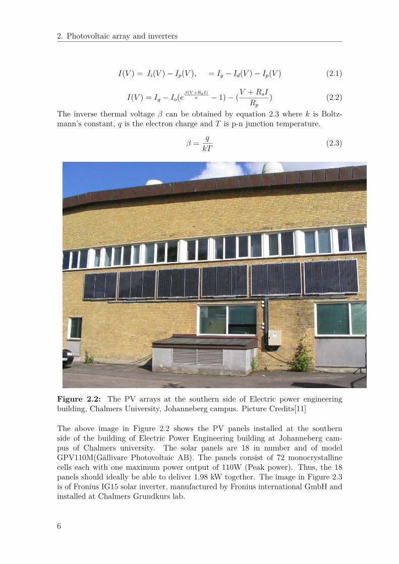
Figure 2.2: The PV arrays at the southern side of Electric power engineeringbuilding, Chalmers University, Johanneberg campus. Picture Credits[11]
The above image in Figure 2.2 shows the PV panels installed at the southernside of the building of Electric Power Engineering building at Johanneberg cam-pus of Chalmers university. The solar panels are 18 in number and of modelGPV110M(Gällivare Photovoltaic AB). The panels consist of 72 monocrystallinecells each with one maximum power output of 110W (Peak power). Thus, the 18panels should ideally be able to deliver 1.98 kW together. The image in Figure 2.3is of Fronius IG15 solar inverter, manufactured by Fronius international GmbH andinstalled at Chalmers Grundkurs lab.
6

2. Photovoltaic array and inverters
Important details of the solar inverter in Grundkurs lab[11].• The inverter model is Fronius IG 15 and it was installed in May 2007,• The inverter has max power of 2 kW and voltage range of 150-400 V,• It has a HF transformer to boost the voltage and the advantages of using the
transformer are:– size of inverter becomes very small,– the inverter becomes light and powerful,– The transformer provides safety due to electrical isolation.
Figure 2.3: Fronius IG 15 inverter installed in Chalmers Grundkurs lab, Johan-neberg campus.
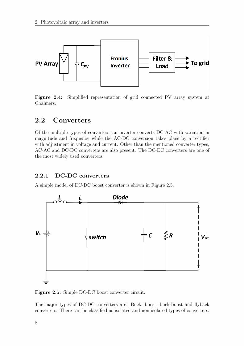
The Figure 2.4 is block representation of grid connection of the PV panels and solarinverter installed at Chalmers Johanneberg campus.
7
2. Photovoltaic array and inverters
Figure 2.4: Simplified representation of grid connected PV array system atChalmers.
2.2 ConvertersOf the multiple types of converters, an inverter converts DC-AC with variation inmagnitude and frequency while the AC-DC conversion takes place by a rectifierwith adjustment in voltage and current. Other than the mentioned converter types,AC-AC and DC-DC converters are also present. The DC-DC converters are one ofthe most widely used converters.
2.2.1 DC-DC convertersA simple model of DC-DC boost converter is shown in Figure 2.5.
Figure 2.5: Simple DC-DC boost converter circuit.
The major types of DC-DC converters are: Buck, boost, buck-boost and flybackconverters. There can be classified as isolated and non-isolated types of converters.
8

2. Photovoltaic array and inverters
The flyback converter belongs to the category of isolated converters while the buck,boost and buck-boost converters belong to the non-isolated converter category. Theisolated converter have a galvanic isolation wherein a transformer is used unlike thenon-isolated converters with no electrical isolation.Apart from the mentioned popular converters, there are other converters as welllike the Ćuk converter and the charge pump. The Ćuk converter is a non-isolatedtype of converter. The function of various DC-DC converters is to vary the suppliedoutput voltage. The boost converter is a voltage step-up converter and buck on theother hand is a voltage step-down converter. Since the power remains constant thecurrent falls in boost while rises in buck converter. The buck-boost can do boththe step-up and step-down of output voltage. The flyback and Ćuk have the samefunction as buck-boost converter. The flyback converter has an isolating factor dueto the presence of transformer separating input from output. The usage varies fromcell phone chargers and LASERS to standby power supplies in PCs. The chargepump converter on the other hand is basically used for low power applications. Itis also similar in function to the buck-boost converter.
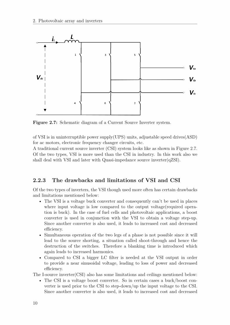
2.2.2 InvertersThe inverters can be classified into two broad types: voltage source inverter(VSI)and current source inverter(CSI). The VSI is a voltage step down/buck inverterwhile the CSI is a voltage boost/step up inverter.The traditional voltage source inverter (VSI) system is as shown in Figure 2.6
Figure 2.6: Schematic diagram of a Voltage Source Inverter system.
The VSI has a voltage source connected in parallel with a large capacitor while CSIhas a current source as input. The CSI directly controls output AC current. Thus,the VSI is a voltage stiff inverter while the CSI is a current stiff inverter. The usage
9
2. Photovoltaic array and inverters
Figure 2.7: Schematic diagram of a Current Source Inverter system.
of VSI is in uninterruptible power supply(UPS) units, adjustable speed drives(ASD)for ac motors, electronic frequency changer circuits, etc.A traditional current source inverter (CSI) system looks like as shown in Figure 2.7.Of the two types, VSI is more used than the CSI in industry. In this work also weshall deal with VSI and later with Quasi-impedance source inverter(qZSI).
2.2.3 The drawbacks and limitations of VSI and CSIOf the two types of inverters, the VSI though used more often has certain drawbacksand limitations mentioned below:
• The VSI is a voltage buck converter and consequently can’t be used in placeswhere input voltage is low compared to the output voltage(required opera-tion is buck). In the case of fuel cells and photovoltaic applications, a boostconverter is used in conjunction with the VSI to obtain a voltage step-up.Since another converter is also used, it leads to increased cost and decreasedefficiency.
• Simultaneous operation of the two legs of a phase is not possible since it willlead to the source shorting, a situation called shoot-through and hence thedestruction of the switches. Therefore a blanking time is introduced whichagain leads to increased harmonics.
• Compared to CSI a bigger LC filter is needed at the VSI output in orderto provide a near sinusoidal voltage, leading to loss of power and decreasedefficiency.
The I-source inverter(CSI) also has some limitations and ceilings mentioned below:• The CSI is a voltage boost converter. So in certain cases a buck/boost con-
verter is used prior to the CSI to step-down/up the input voltage to the CSI.Since another converter is also used, it leads to increased cost and decreased
10

2. Photovoltaic array and inverters
efficiency(because there is another power conversion stage due to extra con-verter).
• High preformance of the IGBT’s is decreased owing to the usage of a seriesdiode in combination.
In addition, both VSI and CSI share the following problems:• Since they are either a voltage buck or voltage boost inverter and not buck-
boost, their application is limited for certain scenarios because of range ofoutput voltage achievable.
• The VSI and the CSI cannot be interchanged i.e. one used in other’s placebecause of the different source needed and output voltage range.
• They are both susceptible to electromagnetic interference(EMI) noise.
2.3 Z-Source Inverter(ZSI)The VSI and CSI have limitations of operation since they can act either as volt-age buck or voltage boost inverter respectively, although extensively utilized in theindustry [12]. Thus a boost converter is attached prior to the VSI in case of fuelcells or photovoltaic applications and similarly another DC-DC converter needs tobe attached prior to a CSI to generate necessary output voltage. Since it is a tediousprocess to control two converters(DC-DC converter and the inverter) along with es-calation in the costs, Z-source inverters(ZSI) are preferable to them. The ZSI is asingle stage inverter with criss-cross of capacitor and inductor to form a X structurebetween the DC source and the inverter. This helps in operating both in the buckand boost mode depending upon requirement. The special network of two inductorand two capacitors uses shoot through state to achieve buck and boost in the sameconfiguration as per the need. In case of a shoot-through state, the switches in thephase leg are simultaneously shorted. It could be one phase leg at a time, two phaselegs or even all of the three.
The configuration of a ZSI is shown in Figure 2.8.
Figure 2.8: Schematic diagram of a Z-Source Inverter system.
11

2. Photovoltaic array and inverters
The Figure 2.8 shows the general Z-source inverter structure consisting of two in-ductors L1 and L2 while capacitors C1 and C2 connected in a criss-cross X shapeto couple the inverter to the DC voltage source.
Figure 2.9: (a) Non shoot-through state equivalent circuit model of ZSI. (b) Shoot-through state equivalent circuit model of ZSI.
In case of usage of photovoltaic cells and fuels cells as DC voltage source, a boostconverter is needed since the output voltage of the cells is highly variable dependingon the irradiation and current drawn from the fuel stack respectively. The boostconverter ensures a step-up of voltage since the VSI is avoltage buck converter. Onthe other hand, ZSI is a single stage inverter capable of producing both the buck andboost of AC output depending on the requirement. The VSI has six active statesand two zero states but in the case of ZSI there is an additional zero state known asthe shoot-through state. Thus, in all a ZSI has nine states. The shoot-through statehelps in achieving a voltage boost if needed. It also ensures no need of blankingtime which is a standard feature of VSIs to avoid source short circuit.The ZSI thus has two operation modes: the regular non shoot-through mode andthe shoot-through mode. The Figure 2.9 shows the equivalent circuits of ZSI at the
12

2. Photovoltaic array and inverters
regular i.e. non shoot-through mode and the extra mode i.e. shoot-through mode.In the non shoot-through mode shown in Figure 2.9(a), the ZSI operates like a VSIor a CSI with the regular eight states(six active and the remaining two zero states)while in the shoot-through mode shown in 2.9(b), the source is shorted across oneor all phase legs forbidden in a traditional inverter.
2.4 Advantages and disadvantages of ZSIThe ZSI in Figure 2.8 interfaces the DC source voltage and the inverter bridge.The ZSI not only has a buck-boost feature but also lacks the traditionally presentblanking time in a regular inverter. The advantages ZSI poses over the traditionalVSI or CSI is not limited but extends to the following:
• The DC source of input is not limited to a battery but can be one of themultitude including voltage or current source or even load like diode rectifier,thyristor converter, inductor, capacitor, etc ;
• The ZSI can be used in a plethora of applications like in variable output voltagesources such as fuel cells and photovoltaic arrays. The AC voltage can thusbe varied to any value in the range of zero to very high magnitudes. The ZSIis a buck-boost inverter which is not a property of VSI or CSI;
• One can use all PWM schemes to control the ZSI. Hence, it offers great flexi-bility as well;
• It can be applied to all ranges of power conversion.
13

2. Photovoltaic array and inverters
Current source inverter Voltage source inverter Z-source inverter
1.The CSI acts as a con-stant current source or cur-rent stiff since a large induc-tor is used in series with thevoltage source
The VSI acts as a constantvoltage source or voltagestiff inverter since a largecapacitor is used in parallelwith the voltage source.
The ZSI acts as a con-stant high impedance volt-age source.
2.High source impedancedue to large inductor con-nected in series with the DCsource.
Low source impedance dueto a capacitor connected inparallel with the DC source.
Since both inductor and ca-pacitor are used in the DClink, it has a constant highimpedance.
3.The CSI is more robuistand has the capacity to bearmisfiring of the switcheswithout danger, hence lesssensitive comparative to theVSI.
Misfiring of switches in aVSI is dangerous since theparallel capacitor shall thefault and hence more sen-sitive to switch misfiringsthan CSI.
The ZSI can also bear mis-firing of the switches some-times though not as much asthe CSI but more than theVSI.
4.Cannot be used in bothbuck or boost operation ofinverter at the same time.
Cannot be used in bothbuck or boost operation ofinverter at the same time.
Can be used in both buckand boost operation of in-verter at the same time.
5.The main circuits are notinterchangeable.
The main circuits are notinterchangeable.
Here the main circuits areinterchangeable.
6.The harmonic distortiontends to be high.
VSI also has quite high har-monic distortion.
Harmonic distortion in ZSItends to be lower.
7.Introduction of filtercauses high power loss.
Introduction of filter causeshigh power loss.
Compared to the VSI andCSI, lower power loss.
8.Observed that power lossdecreases efficiency here.
High power loss decreasesefficiency here.
Comparatively higher effi-ciency due to lower powerloss.
Table 2.1: The comparison of ZSI to CSI and VSI.
14
2. Photovoltaic array and inverters
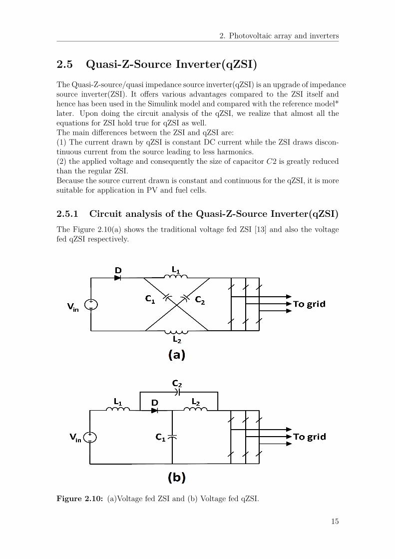
2.5 Quasi-Z-Source Inverter(qZSI)The Quasi-Z-source/quasi impedance source inverter(qZSI) is an upgrade of impedancesource inverter(ZSI). It offers various advantages compared to the ZSI itself andhence has been used in the Simulink model and compared with the reference model*later. Upon doing the circuit analysis of the qZSI, we realize that almost all theequations for ZSI hold true for qZSI as well.The main differences between the ZSI and qZSI are:(1) The current drawn by qZSI is constant DC current while the ZSI draws discon-tinuous current from the source leading to less harmonics.(2) the applied voltage and consequently the size of capacitor C2 is greatly reducedthan the regular ZSI.Because the source current drawn is constant and continuous for the qZSI, it is moresuitable for application in PV and fuel cells.
2.5.1 Circuit analysis of the Quasi-Z-Source Inverter(qZSI)The Figure 2.10(a) shows the traditional voltage fed ZSI [13] and also the voltagefed qZSI respectively.
Figure 2.10: (a)Voltage fed ZSI and (b) Voltage fed qZSI.
15

2. Photovoltaic array and inverters
As is the case with a regular ZSI, the qZSI also has two modes of operation i.e. thenon shoot-through and the shoot-through mode. The effective equivalent circuit of aqZSI under the non shoot-through and shoot-through mode can be seen in the Figure2.11. In the non shoot-through state of Figure 2.11(a), the inverter bridge/switchesresemble a current source while the switches are shorted with VP N equal to zero inthe case of shoot-through state in Figure 2.11(b).
Figure 2.11: The qZSI equivalent circuit under (a) non-shoot-through and (b)shoot-through state.
The Figure 2.11 shows the voltage polarity and current flow directions. If the shoot-through interval is Tsh during a switching cycle of time period T then the shoot-
16

2. Photovoltaic array and inverters
through duty ratio is D = Tsh/T . Similarly the non shoot-through interval is Tnsh =T − Tsh. The Figure 2.11(a) shows a regular non shoot-through state for Tnsh timeperiod, thus the inductor voltage for L1 and L2 shall be
vL1 = Vin − VC1, & vL2 = −VC2, (2.4)Similarly for Tnsh the DC link and diode voltage VP N and vdiode respectively are
VP N = VC1 − vL2 = VC1 + VC2 & vdiode = 0 (2.5)
The Figure 2.11(b) reflects the current directions and voltage of the system for theshoot-through states Tsh, giving voltages
vL1 = Vin + VC2, & vL2 = VC1, (2.6)Similarly for Tsh the DC link and diode voltage VP N and vdiode respectively are
VP N = 0 & vdiode = VC1 + VC2 (2.7)Since the average of inductor voltage for a switching cycle is zero under steady state,from equation 2.4 and 2.6, we obtain
VL1 = Tsh(Vin + VC2) + Tnsh(Vin − VC1)T
= 0 (2.8)
VL2 = Tsh(VC1) + Tnsh(−VC2)T
= 0 (2.9)
Consequently,
VC1 = Tnsh
Tnsh − Tsh
Vin & VC2 = Tsh
Tnsh − Tsh
Vin (2.10)
The peak DC link voltage VP N across the inverter bridge/switches can be foundfrom the equations 2.5, 2.7 and 2.10 and comes out as
VP N = VC1 + VC2 = Tnsh
Tnsh − Tsh
Vin = 11− 2(Tsh/T )Vin = BVin (2.11)
where B is the boost factor of the qZSI. If the system power rating is assumed Pthen we can calculate the average current across inductors L1, L2 as
IL1 = IL2 = Iin = P/Vin (2.12)
17

2. Photovoltaic array and inverters
Using Kirchhoff’s current law and the equation 2.12 for capacitor and diode current,we get
IC1 = IC2 = IP N − IL1 & ID = 2IL1 = IP N (2.13)
Based upon above equations and the equivalent circuit diagram, we can safely ascer-tain that the qZSI inherits all the advantages of ZSI. Infact, the qZSI has advantagesover ZSI itself. Like ZSI, qZSI can buck-boost the input voltage and is more reliablethan the traditional VSI based on the comparison drawn in Table 2.1.
2.6 Modeling of voltage fed Quasi-Z-Source In-verter(qZSI)
2.6.1 The steady state model of qZSIThe Figure 2.11 shows the equivalent circuit of the qZSI [14][15][16][18]. The qZSIinductor current directions and capacitor voltage polarity have also been shown inFigure 2.11. Henceforth, R denotes the series resistance of the capacitors and rdenotes the parasitic resistance of the inductors while the Lf and Cf denote thefilter values shown in Figure 3.9.
In the shoot-through state represented in the Figure 2.11(b), we can derive the cir-cuit equations through the state-space equations, which are[34]
L1 0 0 0
0 L2 0 0
0 0 C1 0
0 0 0 C2
iL1(t)
iL2(t)
vC1(t)
vC2(t)
=
−(R + r) 0 0 1
0 −(R + r) 1 0
0 −1 0 0
−1 0 0 0
iL1(t)
iL2(t)
vC1(t)
vC2(t)
+
1 0
0 0
0 0
0 0
Vin(t)
IP N(t)
which is written as Fx=A1x+B1u.
In the non shoot-through state represented in the Figure 2.11(a), we can derive thecircuit equations through the state-space equations, which are
L1 0 0 0
0 L2 0 0
0 0 C1 0
0 0 0 C2
iL1(t)
iL2(t)
vC1(t)
vC2(t)
=
−(R + r) 0 −1 0
0 −(R + r) 0 −1
1 0 0 0
0 1 0 0
iL1(t)
iL2(t)
vC1(t)
vC2(t)
+
1 R
0 R
0 −1
0 −1
Vin(t)
IP N(t)
which is written as Fx=A2x+B2u.
18

2. Photovoltaic array and inverters
Now we have A = D · A1 + (1 − D) · A2 and B = D · B1 + (1 − D) · B2 obtainedusing the state space average method where D is the shoot-through duty cycle and(1−D) is the non shoot-through duty cycle.
Then we obtain
Fx=Ax+Bu=
−(R + r) 0 D − 1 D
0 −(R + r) D D − 1
1−D −D 0 0
−D 1−D 0 0
iL1(t)
iL2(t)
vC1(t)
vC2(t)
+
1 (1−D)R
0 (1−D)R
0 D − 1
0 D − 1
Vin(t)
IP N(t)
If the system is in steady state then AX+BU=0 where X=[IL1 IL2 VC1 VC2]T ,U=[Vin IP N ]T .
That is
−(R + r)IL1 + (D − 1)VC1 +DVC2 + Vin + (1−D)RIP N = 0
−(R + r)IL2 + (D − 1)VC2 +DVC1 + (1−D)RIP N = 0
(1−D)IL1 −DIL2 + (D − 1)IP N = 0
(1−D)IL2 −DIL1 + (D − 1)IP N = 0
Upon solving we get,
VC1 = 1−D1−2D
Vin − V22
VC2 = D1−2D
Vin − V22
IL1 = IL2 = 1−D1−2D
IP N
where,
V22 = (1−D)(R + 2DR)(1− 2D)2 IP N (2.14)
We can see that the current in the two inductors is same for qZSI under steady state.If we ignore the series resistance R and parasitic inductance r, the V22 becomes zero.It can be seen in equation 2.14. On putting V22 equal to zero , we get
VC1 = 1−D1− 2DVin & VC2 = D
1− 2DVin (2.15)
19

2. Photovoltaic array and inverters
2.6.2 The small signal model of qZSIThe small perturbation of state variables can be mathematically denoted asx = [L1(t) L2(t) vC1(t) vC2(t)]T , whereas the input signals can be denoted asu = [Vin(t) IP N(t)]T and shoot-through duty ratio is denoted by d(t).
If we put the above perturbed variables into Fx=Ax+Bu[17], we get small-signalstate equations given below
Fˆx=Ax+Bu+[(A1 − A2) ·X + (B1 −B2) · U ] · d =
−(R + r) 0 D − 1 D
0 −(R + r) D D − 1
1−D −D 0 0
−D 1−D 0 0
iL1(t)
iL2(t)
vC1(t)
vC2(t)
+
1 (1−D)R
0 (1−D)R
0 D − 1
0 D − 1
Vin(t)
IP N(t)
+
VC1 + VC2 − IP NR
VC1 + VC2 − IP NR
−IL1 − IL2 + IP N
−IL1 − IL2 + IP N
· d(t)
Let I11 = IP N − 2IL, V11 = VC1 + VC2 − IP NR in the above matrix. Upon applyingLaplace transforms to the state equations, they are converted into
sL1iL1(s) = −(R+r)iL1(s)+(D−1)vC1(s)+DvC2(s)+Vin(s)+(1−D)RIP N(s)+V11d(s)(2.16)
sL2iL2(s) = −(R+ r)iL2(s) +DvC1(s) + (D− 1)vC2(s) + (1−D)RIP N(s) + V11d(s)(2.17)
sC1vC1(s) = (1−D)iL1(s)−DiL2(s) + (D − 1)IP N(s) + I11d(s) (2.18)
sC2vC2(s) = −DiL1(s) + (1−D)iL2(s) + (D − 1)IP N(s) + I11d(s) (2.19)
Now, for the sake of simplicity we assume L1 = L2 = L and C1 = C2 = C(thoughC2 is far less than C1, we subtract equation 2.17 from 2.16 and equation 2.19 from2.18 to get
iL1(s)− iL2(s) = sC
LCs2 + (R + r)Cs+ 1 · Vin(s) (2.20)
vC1(s)− vC2(s) = 1LCs2 + (R + r)Cs+ 1 · Vin(s) (2.21)
When we compare the equations 2.14 and 2.20, it is obvious that the inductorcurrents, iL1 and iL2 are different in small perturbation models which shows thedifference in their dynamics[18]. Using equations 2.16 to 2.19, a signal flow graphof qZSI can be obtained as shown in the Figure 2.12.
20

2. Photovoltaic array and inverters
The signal flow graph helps in deducing the transfer functions in equation 3.4 and3.5 using Mason’s gain formula.
Figure 2.12: Signal flow graph used to obtain transfer functions in equation 3.4and 3.5 [18].
The small-signal transfer functions of VC1 and iL2[18] are obtained as below fromthe signal flow graph in above Figure 2.12.
vC1(s) = T1(D − 1) + (1− 2D)(1−D)(T1 + 1)[T1 + (1− 2D)2] · Vin(s) + (1− 2D)(1−D)R + T2(1−D)
T1 + (1− 2D)2 · IP N(s)
+(1− 2D)V11 + T2I11
T1 + (1− 2D)2 · d(s)
(2.22)
iL2(s) = 2T1D(1−D)T2(T1 + 1)[T1 + (1− 2D)2] · Vin(s) + T2(1−D)(1− 2D) + T1R(1−D)
T2[T1 + (1− 2D)2] · IP N(s)
+T2(1− 2D)I11 + T1V11
T2[T1 + (1− 2D)2] · d(s)
(2.23)
where T1 = LCs2 + (R + r)Cs and T2 = Ls+R + r .
21
2. Photovoltaic array and inverters
2.7 Type of control methods for shoot-throughduty cycle
There are ways to develop closed loop control of the power electronics in the qZSI.It can be achieved using the state-space averaging model or small signal modellingcan be done [19][20]. A small signal model has been used to generate the transferfunctions and obtain the closed loop control parameters for the qZSI in this work.But there are a broad range of methods available for controlling the DC link voltageVP N around a value so as to obtain a near stable AC voltage at inverter output.Since the input source is Photovoltaic (PV) array, it has voltage variation basedprimarily on the irradiation available at a place and other factors. For the typeof PV array used in the reference model*, temperature is a factor affecting voltageoutput. For the sake of simplicity it has been assumed constant at standard 25celsius.For application in Simulink model of qZSI controller, it was realized that to use adouble loop control with inner current loop and outer voltage loop controlling theshoot-through duty cycle is a better control strategy. There can be other controlstrategies which might provide far better results.
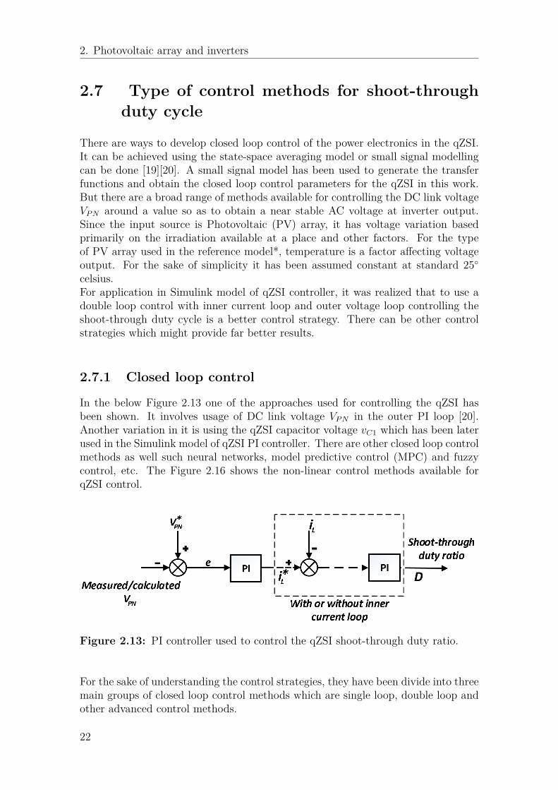
2.7.1 Closed loop control
In the below Figure 2.13 one of the approaches used for controlling the qZSI hasbeen shown. It involves usage of DC link voltage VP N in the outer PI loop [20].Another variation in it is using the qZSI capacitor voltage vC1 which has been laterused in the Simulink model of qZSI PI controller. There are other closed loop controlmethods as well such neural networks, model predictive control (MPC) and fuzzycontrol, etc. The Figure 2.16 shows the non-linear control methods available forqZSI control.
Figure 2.13: PI controller used to control the qZSI shoot-through duty ratio.
For the sake of understanding the control strategies, they have been divide into threemain groups of closed loop control methods which are single loop, double loop andother advanced control methods.
22
2. Photovoltaic array and inverters
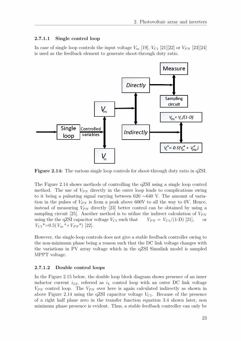
2.7.1.1 Single control loop
In case of single loop controls the input voltage Vin [19], VC1 [21][22] or VP N [23][24]is used as the feedback element to generate shoot-through duty ratio.
Figure 2.14: The various single loop controls for shoot-through duty ratio in qZSI.
The Figure 2.14 shows methods of controlling the qZSI using a single loop controlmethod. The use of VP N directly in the outer loop leads to complications owingto it being a pulsating signal varying between 620 ∼640 V. The amount of varia-tion in the pulses of VP N is from a peak above 600V to all the way to 0V. Hence,instead of measuring VP N directly [23] better control can be obtained by using asampling circuit [25]. Another method is to utilize the indirect calculation of VP N
using the the qZSI capacitor voltage VC1 such that VP N = VC1/(1-D) [21], orVC1*=0.5(Vin*+VP N*) [22].
However, the single-loop controls does not give a stable feedback controller owing tothe non-minimum phase being a reason such that the DC link voltage changes withthe variations in PV array voltage which in the qZSI Simulink model is sampledMPPT voltage.
2.7.1.2 Double control loops
In the Figure 2.15 below, the double loop block diagram shows presence of an innerinductor current iL2, referred as iL control loop with an outer DC link voltageVP N control loop. The VP N over here is again calculated indirectly as shown inabove Figure 2.14 using the qZSI capacitor voltage VC1. Because of the presenceof a right half plane zero in the transfer function equation 3.4 shown later, nonminimum phase presence is evident. Thus, a stable feedback controller can only be
23

2. Photovoltaic array and inverters
obtained with two loops such that the inner loop is comparatively very fast thanthe outer loop. The non minimum phase effects can be countered and qZSI systemstability increased by using a P controller in the inner current loop [20]. A betterstability margin is achievable with inclusion of an integrator as well inside the currentcontrol loop [26]. As stated earlier, in the controller design for the qZSI model, thesimulation investigations of the double-loop control by outer PI controller and innerPI controller have been utilized.
Figure 2.15: The double loop control methods for shoot-through duty ratio inqZSI.
2.7.1.3 Other control methods
As mentioned earlier, there can be another kind of qZSI controllers than the PIcontrollers mentioned in single loop methods. The below Figure 2.16 shows thesemethods. Non linear controllers such as fuzzy controller[27], neural network con-troller[28], sliding controller[29][30] and model predictive controller (MPC)[22] canalso be used in qZSIs. The Vin, VP N , iL and VC1 serve as real time variables togenerate the shoot-through duty cycle.
Figure 2.16: The non-linear control methods of shoot-through duty ratio in qZSI.
In comparison to regular controllers the advanced ones have faster responses yetthe downsides prevent easier adoption. Their application is complex and tediouscompared to the PI controllers which are readily used for the same processes.
24
3Design of qZSI impedance network
and controller
3.1 Designing qZSI impedance networkThe impedance network of the qZSI is comprised of the capacitors C1, C2 and theinductors L1, L2. The carrier wave frequency is 10 kHz, so the shoot throughfrequency fs for simple boost control method is twice of the carrier wave frequency,hence 20 kHz. Since the system operates in boost control mode for our application,we can calculate the maximum shoot through interval T0−max
T0−max = 2−√
3Mmin
fs
(3.1)
The value of T0−max is obtained as 26 µsec for Mmin=0.85.The function of the inductors in the impedance network of qZSI is to limit the ripplein the current during boosting. For convenience sake the inductance of L1= L2=L.
L = VL∆T∆I (3.2)
The value of inductance is calculated as 300 µH. Upon simulation the value ofinductance was varied and optimal value was found to be 100 µH and has beenverified by pole-zero and bode plots.Similarly the calculation of the capacitance value is also done. During the nonshoot-through state the capacitors are in series. The function is to reduce the ripplecontent of voltage on the inverter bridge and consequently the harmonic distortionof the inverter output as well. The value of capacitors are not same but again forthe sake of convenience the values of C1 and C2 are taken equal as C1=C2=C. Itis to be noted that in case of ZSI the values of the capacitance C1=C2 and for in-ductance L1= L2. This is not the case in qZSI during practical conditions wherethe capacitance value C2 is quite small compared to C1. But in order to make thecalculation and simulation easier, such an assumption has been taken here.
C = 2 IC∆T∆(VC1 + VC2) = 300µF (3.3)
25

3. Design of qZSI impedance network and controller
One of the methods to optimize parameters is to use bode plots and determinethe optimum value for the inductor L and capacitor C in impedance network.Theinductance L1 and L2 of the impedance network are represented by L and similarlythe capacitance C1 and C2 are represented by C henceforth. Also pole-zero mapscan also be utilized for the same purpose. The transfer function in equation 3.4is of utmost importance and is used for designing the DC side controller. It is ofperturbations in capacitor voltage vc1 of the qZSI and the shoot-through duty ratiod derived from equation 2.22.
GVc1d(s) = vc1(s)d(s)
= LI1s+ (R + r)I1 + (1− 2D)V1
LCs2 + (R + r)Cs+ (1− 2D)2 (3.4)
Figure 3.1: Changes in poles and zeros upon varying inductance with constantC=300 µF
The transfer function representing perturbations in inductor current iL2 and theshoot-through duty ratio d is as given in equation 3.5 below derived from equation2.23 [18].
GiL2d(s) = iL2(s)d(s)
= (Ls+R + r)(1− 2D)I1 + (LCs2 + (R + r)Cs)V1
(LCs2 + (R + r)Cs)[(Ls+R + r) + (1− 2D)2] (3.5)
In the above transfer function equations 3.4 and 3.5 , I1=IP N − 2IL and V1 =VC1 +
26

3. Design of qZSI impedance network and controller
VC2− IP NR , derived from Figure 2.11 where IL1 is taken equal to IL2 for simplicity.
Figure 3.2: Changes in poles upon varying capacitance with constant L=100 µH
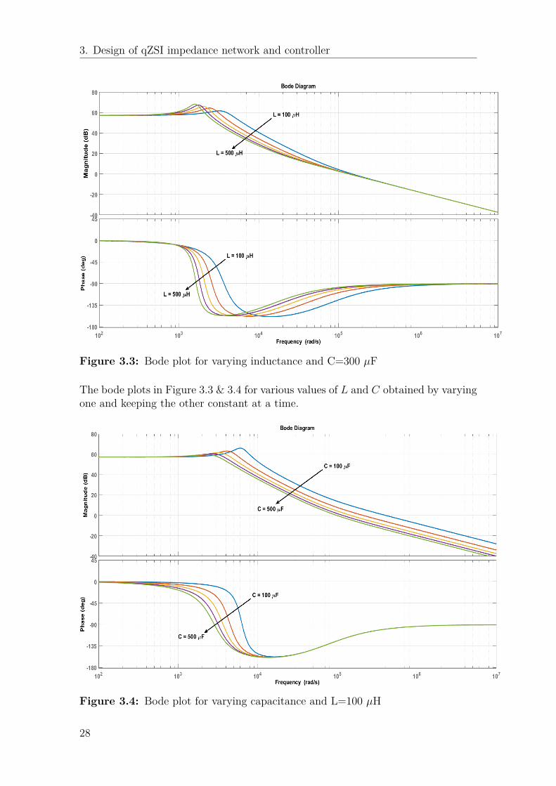
For optimising values of inductance L and capacitance C, both are varied with onekept constant at a time causing observational changes in the movement of polesand zeros. As and by the inductance L is increased from 100 µH to 500 µH inwith capacitance constant at 300 µF the variation in zeros is from negative real axistowards the origin in Figure 3.1. This signifies an increase in the non-minimumphase undershoots, while the movement of poles increases the system settling timeand response. The non-minimum phase undershoot occurs in a lot of convertersand typically is recognized by an undershoot to a step response. In the second casewhen we start varying capacitance C from 100 µF to 500 µF, Figure 3.2 shows theshifting of poles vertically towards the real axis, while the zeros stay constant.With the changes of L and C, the bode plots of the transfer function GVCd areshown in Figure 3.3 and 3.4. It can be seen that when inductance increases, theamplitude–frequency characteristic changes gently and the quality factor decreases.However when the capacitance increases, the amplitude–frequency characteristicchanges steeply and the quality factor increases. Similarly, the resonant frequencyreduces with the two parameters increasing.Thus, the optimised value of the inductance L and capacitance C were found to be100 µ H 300 µ F respectively. The others values for filter and R and r have beenoptimised by simulations.
27
3. Design of qZSI impedance network and controller
Figure 3.3: Bode plot for varying inductance and C=300 µF
The bode plots in Figure 3.3 & 3.4 for various values of L and C obtained by varyingone and keeping the other constant at a time.
Figure 3.4: Bode plot for varying capacitance and L=100 µH
28

3. Design of qZSI impedance network and controller
The values of the parameters used in Simulink model of the qZSI. The value ofshoot-through duty cycle D has been calculated using the boost factor.
L=100 µH C=300 µF
R=0.08 Ω r=0.15 Ω
Lf = 1000µH Cf = 110µF
RL = 5Ω D=0.28
Table 3.1: Parameters used in Simulink qZSI model
3.2 Control strategy of qZSIThe main control strategies of qZSI are the following four[18]:
• Simple boost control,• Maximum boost control[31],• Maximum constant boost control[32],• Modified space vector PWM (MSVPWM) control [34].
Figure 3.5: Implementation of a qZSI to grid connected PV arrays.
In the Simulink model of qZSI, the implementation of control strategy is similar tosimple boost control since it is the simplest of all control strategies.
3.2.1 Sinusoidal PWM and shoot-through implementationThe Pulse width modulation(PWM) strategy used in simulating qZSI is sinusoidalPWM(SPWM). In SPWM a triangular carrier wave and sinusoidal reference waves
29

3. Design of qZSI impedance network and controller
are used for generating signal for switches of the inverter. These signals are gen-erated by comparing the reference wave with the carrier wave. A high signal isgenerated for reference wave > carrier wave. Similarly, a low signal is generated forvice-versa. The shoot through state basically involves the switches being open forlonger time period. This can be accomplished by generating high and low for it andsupplying simulataneously with the SPWM.
The Figure 3.6 illustrates SPWM.
Figure 3.6: Sinusoidal PWM
The Figure 3.7 shows the Simulink block diagram of SPWM and shoot throughsignals supplied to the inverter switches .
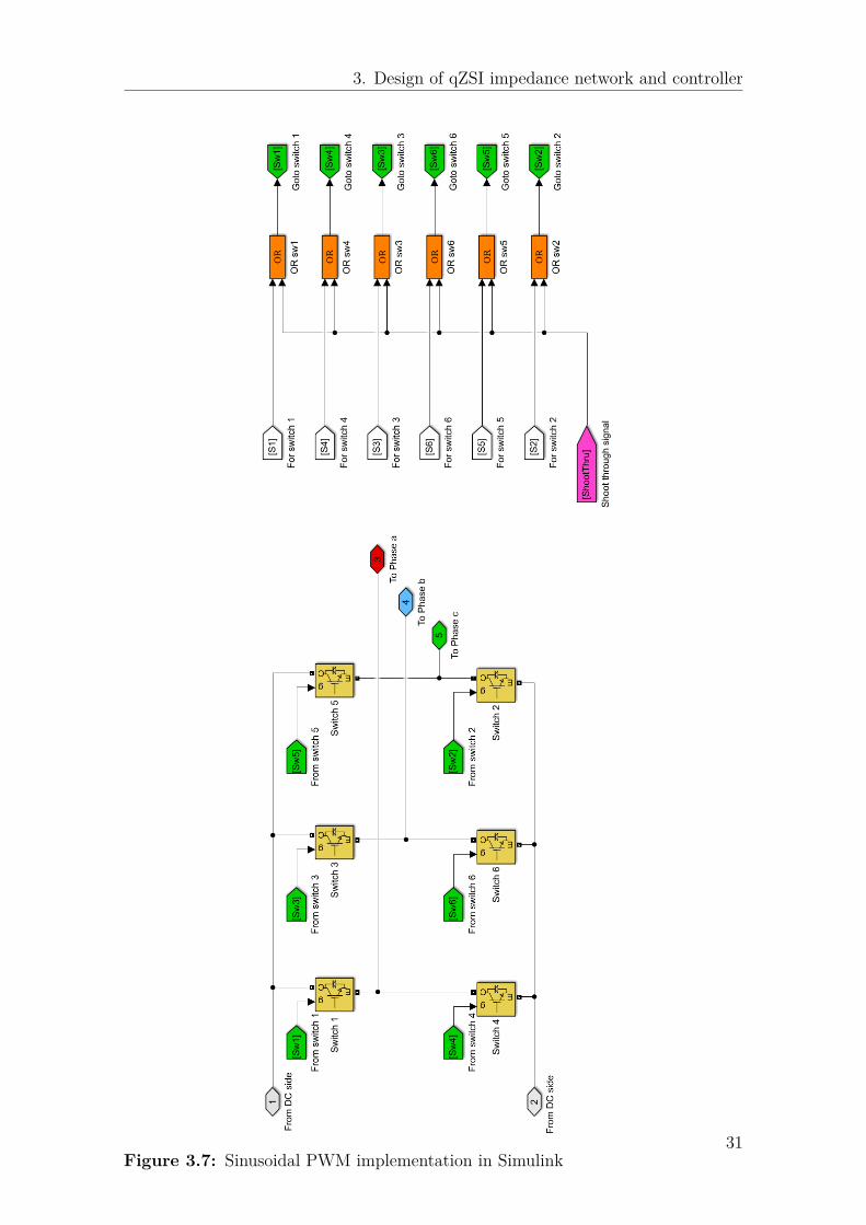
30
3. Design of qZSI impedance network and controller
Figure 3.7: Sinusoidal PWM implementation in Simulink31
3. Design of qZSI impedance network and controller
3.3 DC side controller design for qZSI
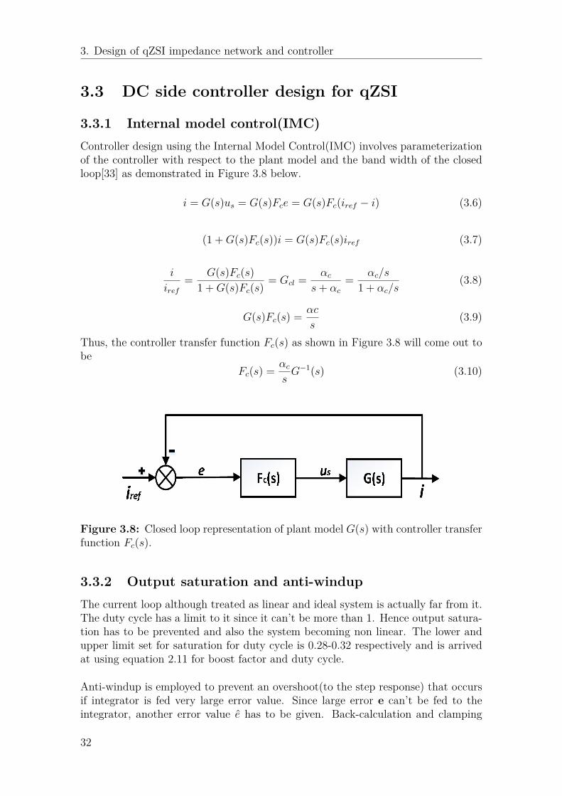
3.3.1 Internal model control(IMC)Controller design using the Internal Model Control(IMC) involves parameterizationof the controller with respect to the plant model and the band width of the closedloop[33] as demonstrated in Figure 3.8 below.
i = G(s)us = G(s)Fce = G(s)Fc(iref − i) (3.6)
(1 +G(s)Fc(s))i = G(s)Fc(s)iref (3.7)
i
iref
= G(s)Fc(s)1 +G(s)Fc(s)
= Gcl = αc
s+ αc
= αc/s
1 + αc/s(3.8)
G(s)Fc(s) = αc
s(3.9)
Thus, the controller transfer function Fc(s) as shown in Figure 3.8 will come out tobe
Fc(s) = αc
sG−1(s) (3.10)
Figure 3.8: Closed loop representation of plant model G(s) with controller transferfunction Fc(s).
3.3.2 Output saturation and anti-windupThe current loop although treated as linear and ideal system is actually far from it.The duty cycle has a limit to it since it can’t be more than 1. Hence output satura-tion has to be prevented and also the system becoming non linear. The lower andupper limit set for saturation for duty cycle is 0.28-0.32 respectively and is arrivedat using equation 2.11 for boost factor and duty cycle.
Anti-windup is employed to prevent an overshoot(to the step response) that occursif integrator is fed very large error value. Since large error e can’t be fed to theintegrator, another error value e has to be given. Back-calculation and clamping
32

3. Design of qZSI impedance network and controller
can be used to implement anti-windup.The error signal e fed to the integrator using back calculation method[33] is
e = e+ Outputlimted −Outputunlimited
Kp
(3.11)
Both saturation and anti-windup are used only in the inner loop of the simulatedqZSI Simulink model.
3.3.3 DC side controllerA block diagram representation of DC side controller[18] is shown in Figure 3.9below. The relation between voltage VP N and VC1 is derived using equation 2.11and 2.15 and serves to calculate VP N error for PI controller input. The inner controlloop is used to generate the shoot-through duty ratio and then shoot-through pulsessupplied along with those of SPWM to the inverter switches maintaining VP N around620 ∼ 640V.
Figure 3.9: The DC side controller design with PI controller in the inner loop
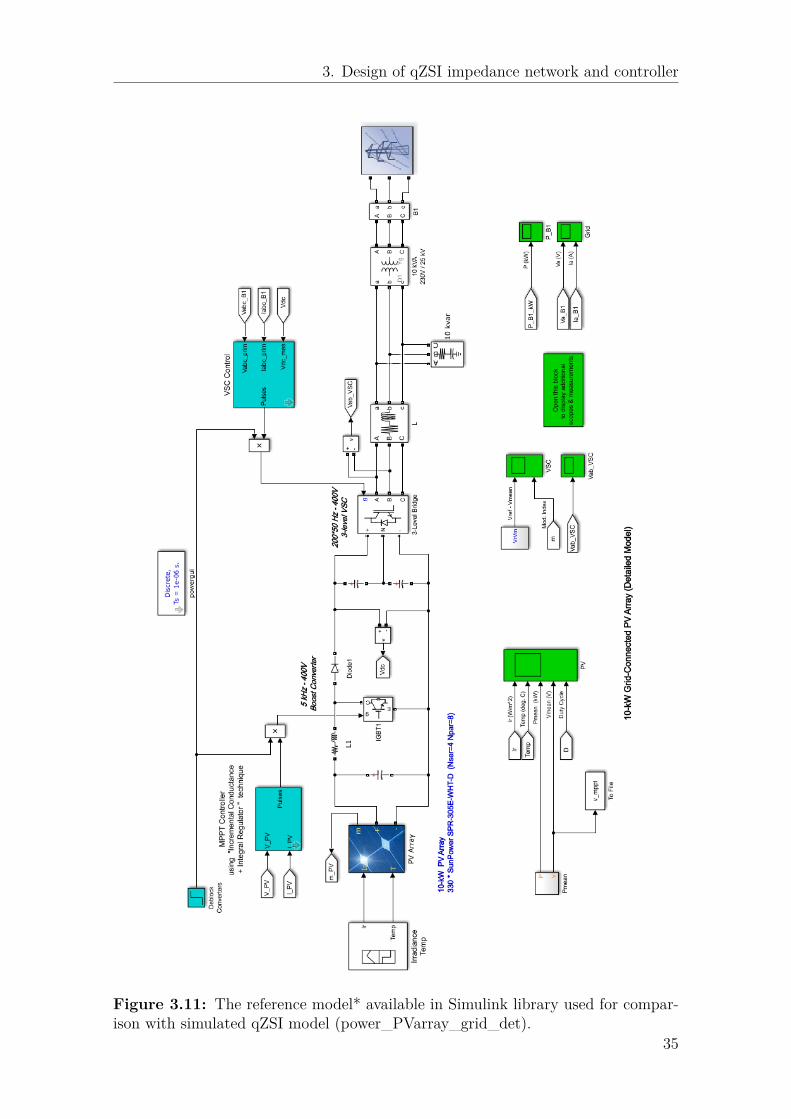
Based on the above Figure 3.9(a) Simulink model has been made. The Figure 3.10is qZSI model made in Simulink and used to compare with the reference model* ofPV array connected VSI supplying power to the grid.It is also compared with the solar inverter installed in Chalmers lab. The referencemodel* used for comparison with the qZSI Simulink model is shown in Figure 3.11.The reference model* is available in the Simulink library(power_PVarray_grid_det)and has been sufficiently modified to compare with the simulated qZSI model.
33

3. Design of qZSI impedance network and controller
Figure 3.10: Simulink model of qZSI used to compare with the reference model*34
3. Design of qZSI impedance network and controller
Figure 3.11: The reference model* available in Simulink library used for compar-ison with simulated qZSI model (power_PVarray_grid_det).
35

3. Design of qZSI impedance network and controller
In order to keep the input same to the inverters, sampled MPPT voltage in Figure3.12 was taken from the reference model* and it serves as qZSI model’s input. Thevariation of MPPT voltage as shown in Figure 3.12 is found to be from 227 V to 321V but under steady state it varies from 250 V to 273.5 V. The qZSI in simulationworks in boost mode all the time, pumping up the voltage DC link voltage = VDcLink
= VP N to about 620 ∼ 640 V for most of the cycle of 1.2 sec to get an AC outputof 230 Vpeak.
Figure 3.12: Sampled MPPT voltage from the reference model*
The DC side controller subsystem in the Figure 3.10 has been derived from the blockdiagram shown in Figure 3.13 below. It consists of two loops: the inner current loopand the outer voltage loop. PI controllers are used in both the loops.
Figure 3.13: Block diagram representation of the closed loop
In the Figure 3.13, the inner loop is inductor L2 current loop and can be taken
36
3. Design of qZSI impedance network and controller
to be very fast compared to the outer loop and hence equal to 1. The outer looprepresents the peak DC link voltage loop.
Figure 3.14: Simplified block diagram representation of the closed loop
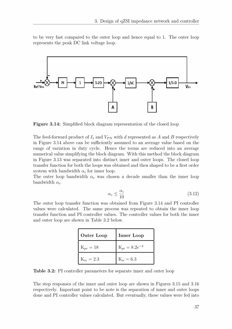
The feed-forward product of I1 and VP N with d represented as A and B respectivelyin Figure 3.14 above can be sufficiently assumed to an average value based on therange of variation in duty cycle. Hence the terms are reduced into an averagenumerical value simplifying the block diagram. With this method the block diagramin Figure 3.13 was separated into distinct inner and outer loops. The closed looptransfer function for both the loops was obtained and then shaped to be a first ordersystem with bandwidth αi for inner loop.The outer loop bandwidth αv was chosen a decade smaller than the inner loopbandwidth αi.
αv ≤αi
10 (3.12)
The outer loop transfer function was obtained from Figure 3.14 and PI controllervalues were calculated. The same process was repeated to obtain the inner looptransfer function and PI controller values. The controller values for both the innerand outer loop are shown in Table 3.2 below.
Outer Loop Inner Loop
Kpv = 18 Kpi = 8.2e−3
Kiv = 2.3 Kii = 6.3
Table 3.2: PI controller parameters for separate inner and outer loop
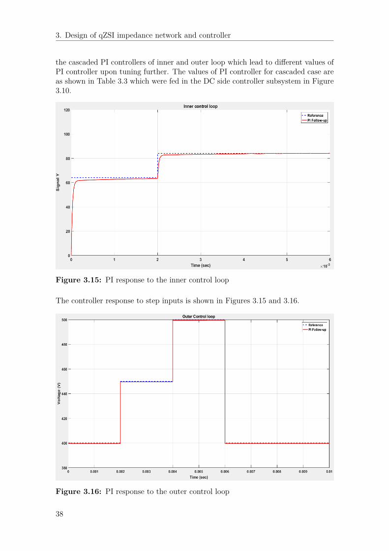
The step responses of the inner and outer loop are shown in Figures 3.15 and 3.16respectively. Important point to be note is the separation of inner and outer loopsdone and PI controller values calculated. But eventually, these values were fed into
37
3. Design of qZSI impedance network and controller
the cascaded PI controllers of inner and outer loop which lead to different values ofPI controller upon tuning further. The values of PI controller for cascaded case areas shown in Table 3.3 which were fed in the DC side controller subsystem in Figure3.10.
Figure 3.15: PI response to the inner control loop
The controller response to step inputs is shown in Figures 3.15 and 3.16.
Figure 3.16: PI response to the outer control loop
38

3. Design of qZSI impedance network and controller
The values in the Table 3.3 below have been used in the final Simulink model ofqZSI with DC side controller, that was compared with the reference model*.
Outer Loop Inner Loop
Kpv = 0.18 Kpi = 8.2e−3
Kiv = 80 Kii = 10
αv = 100π αi = 1000π
Table 3.3: PI controller parameters for cascaded inner and outer loop
39

3. Design of qZSI impedance network and controller
40
4Results and Discussion
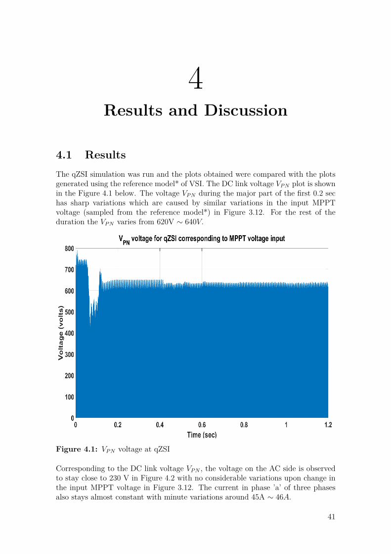
4.1 ResultsThe qZSI simulation was run and the plots obtained were compared with the plotsgenerated using the reference model* of VSI. The DC link voltage VP N plot is shownin the Figure 4.1 below. The voltage VP N during the major part of the first 0.2 sechas sharp variations which are caused by similar variations in the input MPPTvoltage (sampled from the reference model*) in Figure 3.12. For the rest of theduration the VP N varies from 620V ∼ 640V.
Figure 4.1: VP N voltage at qZSI
Corresponding to the DC link voltage VP N , the voltage on the AC side is observedto stay close to 230 V in Figure 4.2 with no considerable variations upon change inthe input MPPT voltage in Figure 3.12. The current in phase ’a’ of three phasesalso stays almost constant with minute variations around 45A ∼ 46A.
41

4. Results and Discussion
Figure 4.2: Output voltage in phase ’a’ of simulated qZSI model
The Figure 4.2 and 4.3 show output voltage and current respectively in phase ’a’.
Figure 4.3: Output current in phase ’a’ of simulated qZSI model
42

4. Results and Discussion
The shoot-through duty cycle value varies from 0.28 to 0.32.
Figure 4.4: Shoot-through duty cycle variation in simulated qZSI model
Figure 4.5: Zoomed shoot-through duty cycle variation in simulated qZSI model
43

4. Results and Discussion
It is for most part of the period of 1.2 sec simulation, that the shoot-through dutyratio varies from 0.28 to 0.32 but during the initial part of the Figure 4.4 it isobserved to be limited to 0.28. This happens because the input voltage goes to ahigh value for that duration and hence the boost ratio is less. Consequently theshoot-through has to be limited to the minimum value possible which is 0.28 here.This shoot-through range was obtained by using the boost factor B which is a ratioof the peak DC link voltage to the input voltage of the qZSI i.e. PV array supplyvoltage to the qZSI. The minimum shoot-through duty ratio also serves as the Dini
for the Matlab script(in Appendix B.2.1) used in the controller portion of the qZSISimulink model.The Fast Fourier Transform(FFT) was done on the output voltage of the Froniusinverter installed in Chalmers Grundkurs lab. It was observed that apart fromthe fundamental, the other harmonics that are present include third, fifth and theseventh harmonics which are prominent compared to rest all harmonics. Yet theTotal Harmonic Distortion(THD) was even less than 1% for the same inverter. Thisis in limit as per the standard IEEE STD 519-2014* [35]. The content of the higherharmonics was found nil in the installed inverter output.
Figure 4.6: FFT of output voltage of the installed inverter in Chalmers lab
The FFT of output voltage of the VSI in reference model* showed minor tracesof even and odd harmonics upto the eighth harmonic. The higher harmonics werefound absent hence limited to the eighth harmonic in both VSI and qZSI cases. Thesame can be checked in the Figure 4.7. In comparison the FFT of qZSI outputvoltage in the simulated model has a more prominent presence of the fifth harmonicwith traces of other odd and even harmonics upto the eighth harmonic.
44

4. Results and Discussion
Figure 4.7: FFT of VSI output voltage in reference model*
The prominent presence of the fifth harmonic can be seen in the Figure 4.8 for qZSI.
Figure 4.8: FFT of qZSI output voltage in phase ’a
45
4. Results and Discussion
Figure 4.9: THD of VSI output voltage in phase ’a’
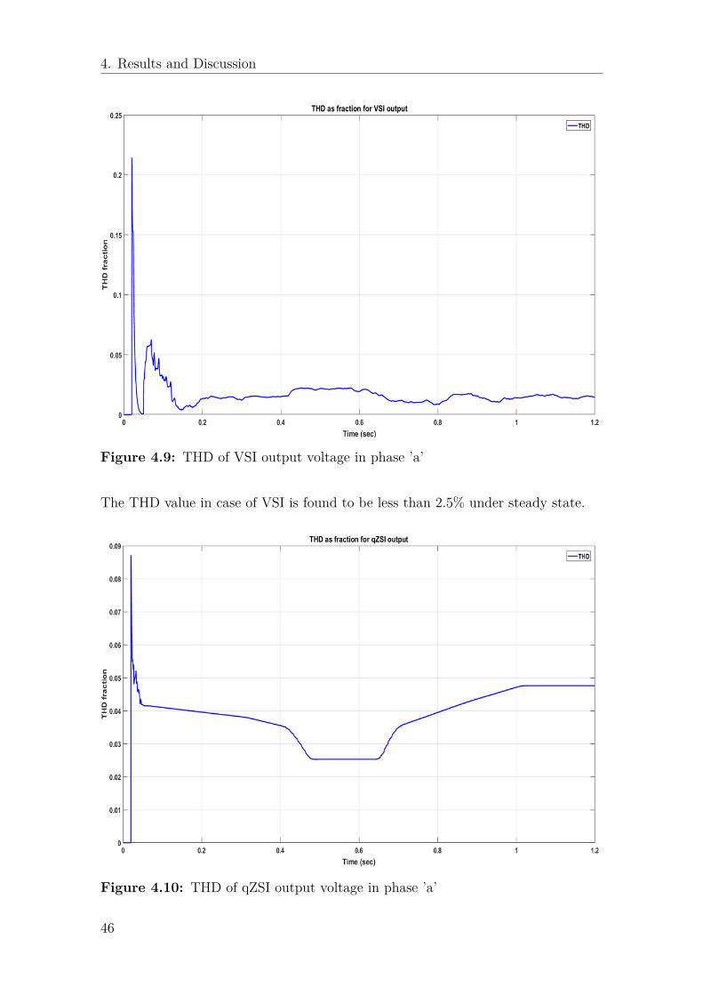
The THD value in case of VSI is found to be less than 2.5% under steady state.
Figure 4.10: THD of qZSI output voltage in phase ’a’
46

4. Results and Discussion
The THD value variation of VSI can be checked in the Figure 4.9.In Figure 4.8, it can be seen that the presence of fifth harmonic is prominently morethan other integer harmonics. The seventh harmonic is also visibly prominent inthe same Figure 4.8. It also has higher harmonic distortion compared to the THDof VSI. The THD of qZSI varies between 2.6% to almost 4.8% Figure 4.10. Thepoint to be noted is that the THD of both the models is lower than the prescribed5% individual harmonic content with the THD % to be less than 8% for voltage ≤1kV(Here voltage is bus voltage at point of common coupling(PCC)) [35].
Though in case of qZSI, it is observed that harmonic content is more than its coun-terpart VSI but this can be attributed to a better filtering in the reference model*.More rigorous filtering in qZSI would have although given less THD but the corre-sponding drop in voltage was also near unavoidable. For the same size of filter, it canbe checked if the output of both inverters has the same THD or if the qZSI THD islower. This will although involve a lot of changes in the VSI reference model* whichfor example can be ranging from the switching frequency of the boost converter tothe VSI switching frequency itself and can be considered one of the future work tasks.
4.2 Sustainable development and ethical aspectsFrom sustainable point of view, upon comparison if the qZSI output has better ef-ficiency and low harmonic distortion then it is a point of attention. It can lead tocertain negative impacts on the environment and society as well.The solar power production shall increase in the next few years till 2022 as per theInternational Energy Agency(IEA)[7]. This means that the need for solar cells isgoing to increase so as to tap more energy. The ill-effects of it on the environmentare glaring and the solar energy is not as clean as it might appear. There are threedimensions of sustainable development and they are all affected [9].The economicaldimension is affected with an increase in price due to higher demand. This formsa vicious circle where escalated demand and increase in price feed each other. Thishas negative impact on the people and the environment which are exploited forminting money. Hence strong regulations are needed for its control. The majorityof solar cells are produced from quartz which comes from silica. The mining of silicais extremely detrimental to the health of miners causing lung disease like silicosis.Usage of hyrdofluoric acid also causes damage to the tissues of the workers in thefactories. It is used to clean the silicon wafers[8]. The new thin film solar cells arenot fully environment friendly either. Compounds like cadmium telluride, cadmiumsulfide and copper indium gallium selenide(CIGS) are used in their manufacturewhich have heavy metal cadmium, a carcinogen and genotoxin[8].It also has ecological dimension where the environment is severely affected. It causespollution of water supplies due to the formation of silicon tetrachloride, acidifyingthe soil and production of harmful fumes[8]. The mining also has an ecological di-mension. It generally leads to the loss of green cover with low rates of forest coverrestoration.The final dimension is the social dimension[9]. With the increase in demand of min-
47

4. Results and Discussion
erals for the solar cell production and consequent ecological destruction, chances areof brewing a social conflict on the regional and inter-regional level. Thus, a toxicfree production of solar cells has to be carried out. The not so sustainable solar cellproduction is becoming more sustainable slowly with the new technologies to makethin film solar cells. But the impact of increasing qZSI PQ is that demand for boththe converter and solar cells will rise. This shall lead to an increase in demand forquartz and feed the circle described in economical dimension before. Thus ecologicaland economical dimension are connected.
In this work, risks related to ethical aspects were mentioned in the section 1.2.Theybasically deal with careful data collection, interpretation of the results and ensuringthe fair presentation of the Fronius inverter information collected through properchannels.
The output voltage and current data collected during the Fronius IG 15 inverteroperation in the Chalmers Grundkurs lab had to be ensured is used for FFT andTHD calculation as was collected and no sloppy data management so as to avoiderror introduction that would lead to incorrect interpretations. Since data fromother sources was also there, it became necessary to avoid any intermixing of it.The second risk corresponded to possibility of wrong interpretations being drawnfrom the results data. Hence the it was published and presented separately for allthe three inverters compared. The FFT and THD data and plots were generatedand showed distinct differences which ensured no mix-ups. The results and plotsfor qZSI voltage and current on the grid side were again easy to make to figureout distinctlyfor them being the only voltage and current plots from Simulink data.Thus, all analysis happened without any mix-up of results’ plots and data.Finally, majority of the data required for Fronius inverter in order to compare wascollected at site and had almost no bearing and impact of the manufacturer whichnegated chances of influencing it for any gains whatsoever. The parameters wereobtained from the manuals, catalogues and purchase order issued by the univer-sity. Hence, it can be deemed untainted. The mitigation of this risk ensures morecredibility of data and removal of other two risks.
48
5Future work and Conclusion
5.1 Future workThe simulation of qZSI model was performed and compared with the referencemodel* of VSI in Simulink. The design of DC side controller was carried out andthe results obtained. But there is always a scope for improvement and future work.Since the model has been made for a DC side controller in qZSI, it can be ex-tended to include AC side controller as well. This will give a chance to counter thedisturbances and the faults which might occur in the AC side.We can also use MPPT voltage with more variations than used in the simulations.Realistic irradiation data from Swedish Meteorological and Hydrological Institute(SMHI) was available at hourly intervals and was hence not used. Data from othersources which is readily available can be used as irradiation source for PV arrays inthe model. The sampling frequency can be increased so as to obtain more samplesper cycle. The sampling frequency was 10 kHz but can be increased to higher limitswhich was avoided due to tiime constraints since it took quite some time to collectmore samples for higher sampling rate.
The PI controller used in the model has been tuned using the IMC method and waslater fine tuned. If fine tuned more, the PI controller can give a better response.Also the qZSI is an upgraded version of ZSI. It has its advantages compared to theZSI such as lower value of capacitor C2 saving costs and continuous DC currentbut there are other upgrades of ZSI also available which have better performancethan the qZSI. Trans-impedance source inverter(TZSI) is another type of ZSI con-verter that is transformer based. The limitations of qZSI and ZSI are a need for alow modulation index and high boost factor to decrease the voltage stress on theinverter bridge. Presence of an impedance network is also considered a drawback.The answer to such issues is a TZSI which has been derived from the ZSI where theinductors have been replaced by the magnetizing inductances of two transformerswhose turns ratio can be used for gain boosting. This TZSI can be further simpli-fied to have only one transformer thus reducing the cost and increasing the voltageboosting ability. Also, in-case of using high switching frequency power devices likeSiC transistor and SiC diodes, the power density shall be increased for the TZSIs.Another improvement can be using other strategies like adaptive neuro fuzzy infer-ence(ANFIS) to predict the optimum modulation index and switch angles requiredfor a improved inverter output voltage[36].
49

5. Future work and Conclusion
5.2 ConclusionThe scope of solar power growth in renewable energy sector is huge considering thesustainable power production being regarded the need of the hour. With danger tothe environment and consequently to the humanity, focus has shifted to renewableenergy for power production all across the globe. Photovoltaics are the major wayto tap the solar energy. Since VSI need a boost converter to step-up the DC voltageprior to conversion, the cascading leads to higher cost. Usage of qZSI and othervariants of ZSI is cost effective comparatively.The design of the impedance network for the qZSI was accomplished by verifyingthe parameters using pole-zero maps and bode plots. It was further confirmed byvalue optimization during the simulations.The PV output varies consequent to the solar irradiation and solar cell temperature.Hence a controller was required to provide a stable DC link voltage for conversionto AC output. Thus, DC side controller was designed for qZSI.It was designed using the IMC principle and the output AC voltage and currentwere obtained at a stable level for various variations in input MPPT voltage. Out-put saturation and anti-windup were considered in the inner current loop design ofDC side controller. The lower and upper limit for saturation were derived for theshoot-through duty cycle. Similarly, antiwindup was used to prevent an overshootin the integrator. Based on their application, stable controller output was achieved.The MPPT voltage was sampled from the reference model* to supply as input inqZSI model so as to maintain uniformity for fair comparison. Upon FFT of out-put voltage it was observed that the concentration of lower odd harmonics was morethan the inverter installed at the Chalmers Grundkurs lab for both Simulink models.The inverter installed in the Chalmers lab is a Fronius International GmbH madeFronius IG 15 model. The lab installed inverter had better THD compared to themodels, though the limit for THD was not breached under any case by any Simulinkmodel. The reference model* also displayed lesser harmonic distortion compared toqZSI model.
Based on the results obtained, it could be safely ascertained that there is a lot ofscope in developing effective control strategies of qZSI and other variants of ZSI forhigher efficiency with lower harmonic distortion. The renewable energy is going tosee major drive in future.
50

Bibliography
[1] SMHI, “SMHI Öppna data”, Mar 15, 2017. [online]. Available:http://opendata-catalog.smhi.se/explore/
[2] L. Aguilar, “Solar energy in Sweden-an implementation plan”, Master’s thesis,Institutionen för kulturgeografi och ekonomisk geografi, Lund University,Lund, Sweden, 2013 .
[3] S. Kok, “Examining solar energy policy in China and India: A comparativestudy of the potential for energy security and sustainable development”,Master’s thesis, Department of Earth Sciences, Uppsala University, Uppsala,Sweden, 2015.
[4] J. L. Sawin et al, “Renewables 2016 Global status report”, REN21, pp. 60-67,2016.
[5] J. M. Guerrero et al, “Wireless-control strategy for parallel operation ofdistributed-generation inverters”, IEEE Transaction on Industrial Electron-ics(IEEE IE), pp. 1461–1470, Octo. 2006.
[6] G. Weiss et al, “H∞ repetitive control of dc-ac converters in microgrids,”IEEE Transaction on Power Electronics(IEEE TPEL), pp. 219-230, Jan. 2004.
[7] International Energy Agency (IEA), “Renewables 2017: Analysis and forecaststo 2022- Executive summary”, Market report series, France, Oct. 2017.
[8] D. Mulvaney, “Solar Energy Isn’t Always as Green as You Think”, IEEESpectrum, Nov 13, 2014. [online]. Available: https://spectrum.ieee.org/green-tech/solar/solar-energy-isnt-always-as-green-as-you-think
[9] F. Hedenus et al, “Sustainable development: History, definition & the role ofthe engineer”, 2015.
[10] A. Yazdani et al, “Modeling guidelines and a benchmark for power systemsimulation studies of three-Phase single-stage photovoltaic systems”, IEEETransaction on Power Delivery(IEEE PWRD), Apr. 2011
51

Bibliography
[11] P. Andersson et al, Inkoppling av solcellsanläggning till elnät, Bachelor’s thesis,Institutionen för Energi och Miljö, Chalmers Tekniska Högskola, Göteborg,Sweden, Maj 2007.
[12] E. Twining et al, “Grid current regulation of a three-phase voltage sourceinverter with an LCL input filter”, IEEE Transaction on Power Electron-ics(IEEE TPEL), pp. 888–895, May 2003.
[13] F. Zheng Peng, “Z-source inverter”, IEEE Transaction on Industrial Applica-tions(IEEE IA), pp. 504-510, Mar-Apr. 2003.
[14] P. C. Loh et al, “Transient modeling and analysis of Pulsewidth modulatedZ-source inverter”, IEEE Transaction on Power Electronics(IEEE TPEL), pp.498–507, Mar. 2007.
[15] J. Liu et al, “Dynamic modeling and analysis of Z-source converter:Derivationof AC small signal model and design-oriented analysis”, IEEE Transaction onPower Electronics(IEEE TPEL), pp. 1786–1796, Sep. 2007.
[16] Y. Li et al, “Modeling and control of Quasi-Z-source inverter for distributedgeneration applications”, IEEE Transaction on Industrial Electronics(IEEEIE), pp. 1532–1541, Apr. 2013.
[17] G. N. V. Prakash, M. K. Kazimierczuk, “Small-signal modeling of open-loopPWM Z-source converter by circuit averaging technique”, IEEE Transactionon Power Electronics(IEEE TPEL), pp. 1286–1296, Mar. 2013.
[18] Y. Liu et al, Impedance Source Power Electronic Converters, 1st ed., JohnWiley & Sons Ltd, 2016, pp. 22-75.
[19] Y. Liu et al, “Z-source/quasi-Z-source inverters:Derived networks, modula-tions, controls and emerging applications to photovoltaic conversion”, IEEEIndustrial Electronics Magazine, pp. 32–44, Dec. 2014.
[20] S. Bacha, I. Munteanu, A. I. Bratcuet, Power Electronic Converters Modelingand Control: with Case Studies, 1st ed., Wiley & Sons Ltd, 2013.
[21] A. Yazdani, R. Iravani, Voltage-Sourced Converters in Power Systems: Model-ing, Control and Applications, 1st ed., Wiley & Sons Ltd, 2010.
[22] M. Mosa et al, “High performance predictive control applied to threephase grid connected Quasi-Z-source inverter”, In Annual Conference of theIEEE Industrial Electronics Society(IEEE IECON 2013), pp. 5812–5817, 2013.
[23] Y. Li et al, “Modeling and control of Quasi-Z-source inverter for distributedgeneration applications”, IEEE Transaction on Industrial Electronics(IEEE
52
Bibliography
IE), pp. 1532–1541, Apr. 2013.
[24] X. Ding et al, “A direct dc-link boost voltage PID-like fuzzy control strategy inZ-source inverter”, In IEEE on Power Electronics Specialists Conference(IEEEPESC 2008), pp. 405–411, 2008.
[25] C. J. Gajanayake et al, “Development of a comprehensive model and amultiloop controller for Z-source inverter DG systems”, IEEE Transaction onIndustrial Electronics(IEEE IE), pp. 2352–2359, Aug 2007.
[26] Q. V. Tran et al, “Minimization of voltage stress across switching devicesin the Z-source inverter by capacitor voltage control”, Journal of PowerElectronics(JPE), pp. 335–342, May 2009.
[27] H. Abu-Rub et al, “Quasi-Z-source inverter-based photovoltaic generation sys-tem with maximum power tracking control using ANFIS”, IEEE Transactionon Sustainable Energy(IEEE STE), pp. 11–20, Jan.2 013.
[28] H. Rostami et al, “Neural networks controlling for both the DC boost andAC output voltage of Z-source inverter”, In of the Power Electronics DriveSystems and Technologies Conference(PEDSTSC 2010), pp. 135–140, Feb.2010.
[29] A. H. Rajaei et al, “Sliding-mode control of Z-source inverter”, In of IEEEAnnual Conference on Industrial Electronics(IEEE IECON 2008), pp. 947–952,Nov. 2008.
[30] J. Liu et al, “A digital current control of Quasi-Z-source inverter with battery”,IEEE Transaction on Industrial Informatics(IEEE II), pp. 928–937, May 2013.
[31] F. Z. Peng et al, “Maximum boost control of the Z-source inverter”, IEEETransaction on Power Electronics(IEEE TPEL), pp. 833–838, Jul-Aug. 2005.
[32] M. S. Shen et al, “Constant boost control of the Z-source inverter to minimizecurrent ripple & voltage stress”, IEEE Transaction on Industrial Applica-tions(IEEE IA), pp. 770-778, May-Jun. 2006.
[33] S.L. Sanjuan, “Voltage Oriented Control of Three-Phase Boost PWM Con-verters”, Master’s thesis, Department of Energy and Environment, ChalmersUniversity of Technology, Gothenburg, Sweden, 2010.
[34] Y. Liu et al, “Modeling and SVPWM control of Quasi-Z-source inverter”, InInternational Conference on Electrical Power Quality and Utilisation(EPQU2011), pp. 1–7, 2011.
53

Bibliography
[35] “IEEE Std 519-2014(Revision of IEEE Std 519-1992)-IEEE recommended prac-tice and requirements for harmonic control in electric power systems”, Mar. 15,2014. [online]. Available: https://standards.ieee.org/findstds/standard/519-2014.html
[36] T.R.Sumithira, A.N. Kumar “Elimination of harmonics in multilevel invert-ers connected to solar photovoltaic systems using ANFIS: An experimentalcase study”, Journal of Applied Research & Technology, pp. 124-132, Feb. 2013.
[37] S. B. Kjaer, “Design and Control of an Inverter for Photovoltaic Applications”,PhD thesis, Institut for Energiteknik, Aalborg Universitet, Aalborg, Denmark,2005.
[38] M. A. Hussain et al. “Comparative assessment of maximum power pointtracking procedures for photovoltaic systems”, Green Energy & Environment,pp. 5-17, Jan. 2017.
54

AAppendix
A.1 IEEE Standard STD 519-2014For the voltage V at point of common coupling(PCC) the individual harmonic con-tent should be less than 5% and the THD should be less than 8% such that V≤1kV[35].
A.2 Maximum power point tracking(MPPT)In distributed power generation like PV array, power generated is susceptible tovariation in the irradiance(W/m2) and temperature of the PV cells.
Figure A.1: I-V and P-V characteristic plot of PV array used in simulation.
I

A. Appendix
The maximum power extraction through PV array is hence a method of varying theresistance visible(of the connected load) to the PV array so that the operating pointand the maximum power point coincide or are closeby for the respective array.The PV array used in the reference model* is SunPower SPR-305E-WHT-Dwith I-V and P-V characteristics as shown in Figure A.1.In order to extract maximum power from the PV array a multitude of MPPT modelsare used. Of all the MPPT models, most common are the following four models:
• Perturb and observe/Hill climbing• Incremental conductance• Current Sweep and• Constant voltage.
The MPPT algorithm is applied for DC-DC boost converter followed by a VSI con-trolling the duty cycle of the boost converter in the reference model*. For the qZSI,sampled MPPT voltage from the reference model* is used as input.In the MPPTlogic variation of duty cycle is employed to vary the observed resistance(reflectedon the PV array side). The variation in duty cycle and hence resistance leads tocoincidence of the actual load line with the load line passing through the maximumpower point. Since incremental conductance logic is used in simulations, only it hasbeen explained below. There are other models as well like Droop method, Fuzzylogic based, Neural network based, Particle swarm optimization MPPT, et cetra.The other MPPT logics can be accessed at [37] and [38].
A.2.1 Incremental conductanceDuring the modelling of MPPT controller, incremental conductance logic is utilized.The current can be expressed as a function of voltage iP V = F (uP V ). At the maximaof the P-V characteristic plot, the gradient or the first order differential of PowerP to voltage uP V is equal to zero. The same property is utilized to arrive at theconclusion that at the maximum power point, the instantaneous conductance value(−iP V /uP V ) and the incremental conductance value (diP V /duP V ) are the same. Thisis shown in the eqn A.1.
dPP V
duP V
= 0
(duP V ).(diP V )duP V
= 0
iP V + diP V
duP V
.uP V = 0
diP V
duP V
= − iP V
uP V
∆iP V
∆uP V
= − iP V
uP V
(A.1)
II

A. Appendix
A.3 Matlab Script
A.3.1 Duty cycle function in controller subsystemfunction y = fcn(u)
persistent Dini;
if isempty(Dini)Dini = 0.28;u = Dini;y = Dini;elseDini = u;y = Dini;end
III