SERVICE MANUAL - Diagramas dediagramas.diagramasde.com/audio/RX-5000VBK.pdf ·...
16
SERVICE MANUAL AUDIO/VIDEO CONTROL RECEIVER No.20883 Nov. 2000 COPYRIGHT 2000 VICTOR COMPANY OF JAPAN, LTD. RX-5000VBK RX-5001VGD UF US China Singapore Area Suffix Contents Safety precautions ---------------- 1-2 Disassembly method ------------- 1-3 Adjustment method --------------- 1-5 Description of major ICs --------- 1-6 Internal connections for FL display tube ----- 1-15 4 1 7 4 1 RM-SR558U REMOTE CONTROL TAPE/MD FM/AM VCR DVD SOUND CONTROL SLEEP 8 3 2 1 5 SURROUND TEST DELAY 6 5 4 EFFECT – CENTER + 5 9 8 7/P – REAR•L + 5 TV VCR AUDIO CD +10 10 – REAR•R + MENU ENT 5 + TV CH – TV/VIDEO PHONO CD-DISC – + TV VOL. DVD MULTI – – ONE TOUCH OPERATION VCR CH + + MUTING VOLUME £ POWER RX-5000V AUDIO/VIDEO CONTROL RECEIVER STANDBY PHONES SPEAKERS 1 2 ADJUST BASS BOOST SETTING MEMORY DVD MULTI CD DVD PHONO VCR TAPE/MD SOURCE NAME FM SURROUND MULTI CURSOR INPUT ATT. ONE TOUCH OPERATION AM MASTER VOLUME – + OFF _ON POWER RX-5000VBK RX-5001VGD
Transcript of SERVICE MANUAL - Diagramas dediagramas.diagramasde.com/audio/RX-5000VBK.pdf ·...

SERVICE MANUALAUDIO/VIDEO CONTROL RECEIVER
No.20883Nov. 2000
COPYRIGHT 2000 VICTOR COMPANY OF JAPAN, LTD.
RX-5000VBKRX-5001VGD
UFUS
ChinaSingapore
Area Suffix
Contents
Safety precautions ---------------- 1-2Disassembly method ------------- 1-3Adjustment method --------------- 1-5
Description of major ICs --------- 1-6Internal connections for FL display tube ----- 1-15
4
1
7
4
1
RM-SR558U REMOTE CONTROL
TAPE/MD
FM/AM
VCR
DVDSOUND
CONTROL
SLEEP
8
321 5
SURROUNDTESTDELAY
654EFFECT – CENTER +
5
987/P – REAR•L +5
TV VCR AUDIOCD
+1010 – REAR•R +
MENU
ENT
5
+TV CH
–TV/VIDEOPHONO
CD-DISC
– +TV VOL.DVD MULTI
––
ONE TOUCHOPERATION
VCR CH
++
MUTING VOLUME
£
POWER
RX-5000V AUDIO/VIDEO CONTROL RECEIVER
STANDBY
PHONES
SPEAKERS
1 2
ADJUSTBASS BOOST
SETTING
MEMORY
DVD MULTI
CD
DVD
PHONO
VCR
TAPE/MD
SOURCE NAME
FM SURROUND MULTI CURSOR
INPUT ATT.
ONE TOUCH OPERATION
AM
MASTER VOLUME
– +
OFF_ ON
POWER
RX-5000VBKRX-5001VGD

RX-5000VBK/RX-5001VGD
1-2
Safety Precautions
1. This design of this product contains special hardware and many circuits and components specially for safety purposes. For continued protection, no changes should be made to the original design unless authorized in writing by the manufacturer. Replacement parts must be identical to those used in the original circuits. Services should be performed by qualified personnel only.
2. Alterations of the design or circuitry of the product should not be made. Any design alterations of the product should not be made. Any design alterations or additions will void the manufacturer`s warranty and will further relieve the manufacture of responsibility for personal injury or property damage resulting therefrom.
3. Many electrical and mechanical parts in the products have special safety-related characteristics. These characteristics are often not evident from visual inspection nor can the protection afforded by them necessarily be obtained by using replacement components rated for higher voltage, wattage, etc. Replacement parts which have these special safety characteristics are identified in the Parts List of Service Manual. Electrical components having such features are identified by shading on the schematics and by ( ) on the Parts List in the Service Manual. The use of a substitute replacement which does not have the same safety characteristics as the recommended replacement parts shown in the Parts List of Service Manual may create shock, fire, or other hazards.
4. The leads in the products are routed and dressed with ties, clamps, tubings, barriers and the like to be separated from live parts, high temperature parts, moving parts and/or sharp edges for the prevention of electric shock and fire hazard. When service is required, the original lead routing and dress should be observed, and it should be confirmed that they have been returned to normal, after re-assembling.
5. Leakage currnet check (Electrical shock hazard testing)After re-assembling the product, always perform an isolation check on the exposed metal parts of the product (antenna terminals, knobs, metal cabinet, screw heads, headphone jack, control shafts, etc.) to be sure the product is safe to operate without danger of electrical shock.Do not use a line isolation transformer during this check.
Plug the AC line cord directly into the AC outlet. Using a "Leakage Current Tester", measure the leakage current from each exposed metal parts of the cabinet , particularly any exposed metal part having a return path to the chassis, to a known good earth ground. Any leakage current must not exceed 0.5mA AC (r.m.s.)Alternate check methodPlug the AC line cord directly into the AC outlet. Use an AC voltmeter having, 1,000 ohms per volt or more sensitivity in the following manner. Connect a 1,500 10W resistor paralleled by a 0.15 F AC-type capacitor between an exposed metal part and a known good earth ground.Measure the AC voltage across the resistor with the AC voltmeter. Move the resistor connection to eachexposed metal part, particularly any exposed metal part having a return path to the chassis, and meausre the AC voltage across the resistor. Now, reverse the plug in the AC outlet and repeat each measurement. voltage measured Any must not exceed 0.75 V AC (r.m.s.). This corresponds to 0.5 mA AC (r.m.s.).
Warning1. This equipment has been designed and manufactured to meet international safety standards.2. It is the legal responsibility of the repairer to ensure that these safety standards are maintained.3. Repairs must be made in accordance with the relevant safety standards.4. It is essential that safety critical components are replaced by approved parts.5. If mains voltage selector is provided, check setting for local voltage.
Good earth ground
Place this probe on each exposedmetal part.
AC VOLTMETER(Having 1000 ohms/volts,or more sensitivity)
1500 10W
0.15 F AC TYPE
! CAUTION Burrs formed during molding may be left over on some parts of the chassis. Therefore, pay attention to such burrs in the case of preforming repair of this system.
RX-5000VBK/RX-5001VGD
1-3
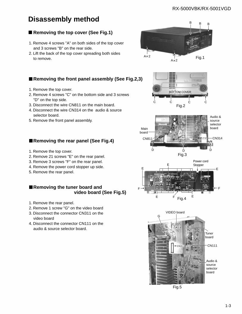
Disassembly method
Removing the top cover (See Fig.1)
1. Remove 4 screws "A" on both sides of the top cover and 3 screws "B" on the rear side. 2. Lift the back of the top cover spreading both sides to remove.
Removing the front panel assembly (See Fig.2,3)
1. Remove the top cover.2. Remove 4 screws "C" on the bottom side and 3 screws "D" on the top side.3. Disconnect the wire CN811 on the main board.4. Disconnect the wire CN314 on the audio & source selector board.5. Remove the front panel assembly.
Removing the rear panel (See Fig.4)
1. Remove the top cover.2. Remove 21 screws "E" on the rear panel. 3. Remove 3 screws "F" on the rear panel. 4. Remove the power cord stopper up side.5. Remove the rear panel.
Removing the tuner board and video board (See Fig.5)
1. Remove the rear panel.2. Remove 1 screw "G" on the video board3. Disconnect the connector CN311 on the video board4. Disconnect the connector CN111 on the audio & source selector board.
A 2A 2
B B B
Fig.1
C C C CFig.2
BOTTOM COVER
Fig.4
Power cordStopperE
CN311
GVIDEO board
Fig.5
Audio &sourceselectorboard
Tunerboard
CN111
D D D
Fig.3
CN811 CN314
Mainboard
Audio &sourceselectorboard
FF
F
E E
EE

RX-5000VBK/RX-5001VGD
1-4
Removing the audio & source selector board (See Fig.6)
1. Remove the rear panel.2. Remove the video board and Tuner board.3. Disconnect the connector CN512 and CN619 on the audio & source selector board. 4. Disconnect to the card wire CN314 on the audio & source selector board.5. Disconnect the connector CN712 on the AMP board.6. Each tie band is cut out.7. Pullout the connection board.8. Remove 4 screws "H" on the audio & source selector board.9. Remove the audio & source selector board.
Removing the main board (See Fig.6 to 8)
1. Remove the rear panel and front panel assembly.2. Pull out the pre AMP board and connection board.3. Remove 8 screws "I" on the main board.4. Remove 8 screws "J" on the power transistor. 5. Disconnect the connector CN511 and wire CN831 on the main board.6. Each tie band is cut out.7. Remove 2 screws "K" on push switch of the front side.8. Remove nut on terminal of the headphone.9. The solder of the wire connected with the transformer is removed.10. Remove the main board.
Removing the front board (See Fig.9)
1. Remove the top cover.2. Remove the Front panel assembly.3. Remove the master volume knob and nut.4. Remove the 13 screws "L" on the Front board.
CN712
H
H
H
Connection board(Standing substrate)
H
CN512
CN314
Fig.6
Audio & sourceselector boardAudio & sourceselector board
Fig.8NUT
K K
Headphone jack
Fig.9
L
L
L
L L L
L
CN511
Pre AMP board(Standing substrate)
CN831
J
MainPCB
Fig.7IIII
I
I
I
Solder
Solder
Audio & sourceselector board
Connectionboard
CN619
RX-5000VBK/RX-5001VGD
1-6
1
2
3
4
5
6
7
8
9
10
11
12
13
14
15
16
17
18
19
20
21
42
41
40
39
38
37
36
35
34
33
32
31
30
29
28
27
26
25
24
23
22
OUT4
OUT3
OUT2
OUT1
AVDD
SWIN
GNDS
SRin
SLin
GNDC
Cin
GNDR
Rin
GNDL
Lin
BYPASSR
BYPASSL
LTRE
LBASS3
LBASS2
LBASS1
DVDD
CLK
DATA
LATCH
DGND
AGND
SWout
SRout
SLout
Cout
Rout
Lout
AVSS
CL1
CL2
CR1
CR2
RTRE
RBASS3
RBASS2
RBASS1
OUT-PUTPORT volume
volume
volume
volume
volume
volume
MCU
I/F
tone tone
1.Block DiagramM62446FP(IC341) : 6CH Master volume
Description of major ICs

RX-5000VBK/RX-5001VGD
1-7
123456789101112131415
16,1718
19~2122
23,24252627282930313233343536373839404142
SURROUNDBASS BOOST
INPUT-ATTMUTING
AVDDSWINA.GNDRR INRL IN
A.GNDC IN
A.GNDR IN
A.GNDL IN
AVSSL OUTR OUTC OUTRL OUTRR OUTSW OUTA.GNDD.GND
VOL STBVOL DATAVOL CLK
DVDD
OOOO-I-II-I-I-I---O---IOI-OOOOOO--III-
SURROUND control terminalBASS BOOST control terminalInput attenuator control terminalMUTING control terminalAnalog positive power supply terminalSUB Woofer volume signal input terminalAnalog ground terminalR ch volume signal input terminal for rear speakerL ch volume signal input terminal for rear speakerAnalog ground terminalCenter volume signal input terminalAnalog ground terminalR ch volume signal input terminalAnalog ground terminalL ch volume signal input terminalNon connectFrequency adjustment terminal tone/trebleFrequency adjustment terminal tone/bassTone output terminalFrequency adjustment terminal tone/bassFrequency adjustment terminal tone/trebleFrequency adjustment terminal tone/bassL/R volume input terminalTone output terminalL/R volume input terminalAnalog negative power supply terminalL ch outputR ch outputCenter volume signal output terminalL ch volume signal output terminal for rear speakerR ch volume signal output terminal for rear speakerSUB Woofer volume signal output terminal Analog ground terminalDigital ground terminalLatch input terminalVolume data input terminalClock input terminal for data transferDigital power supply terminal
Pin No. Symbol I/O Descriptions
2.Pin Function

RX-5000VBK/RX-5001VGD
1-8
2. Pin Function
PinNo. Symbol I/O Function FunctionI/OSymbol
PinNo.
1
2
3
4
5
6
7
8
9
10
11
12
13
14
15
FM IN
AM MIX
FM IF
AM IF
GND
TUNED
STEREO
VCC
FM DET
AM SD
FM VSM
AM VSM
MUTE
FM/AM
MONO/ST O
I
I/O
O
O
I
O
I
I
I
O
O
IIII
I
This is an input terminal of FM IFsignal.
This is an out put terminal for AMmixer.
Bypass of FM IF
Input of AM IF Signal.
This is the device ground terminal.
When the set is tunning,this terminal
becomes "L".
Stereo indicator output. Stereo "L",Mono: "H"
This is the power supply terminal.
FM detect transformer.
This is a terminal of AM ceramic filter.
Adjust FM SD sensitivity.
Adjust AM SD sensitivity.
When the signal of IF REQ of IC121(
LC72131) appear, the signal of FM/AM
IF output. //Muting control input.
Change over the FM/AM input.
"H" :FM, "L" : AM
Stereo : "H", Mono: "L"
16
17
18
19
20
21
22
23
24
25
26
27
28
29
30 OSC BUFFER
AM OSC
REG
AM RF
AFC
AM AGC
O
I
O
I
I
I
AM Local oscillation Signal output.
This is a terminal of AM Localoscillation circuit.
Register value between pin 26 and pin28
besides the frequency width of the
input signal.
AM RF signal input.
This is an output terminal of voltage
for FM-AFC.
This is an AGC voltage input terminal
for AM
O
O
I
O
AM detection output.
FM detection output.
Mpx input terminal
O
O
I
Right channel signal output.
Left channel signal output.
Input terminal of the Right channel post
AMP.
Input terminal of the Left channel
post AMP.I
O
Mpx Left channel signal output.
Mpx Right channel signal output.
R OUT
L OUT
R IN
L IN
RO
LO
IF IN
FM OUT
AM DET
1. Block Diagram
ALC
BUFF
AM
OSC
REG
AMMIX
FMRF.AMP
AGC
AM IF DET
SDCOMP
AMS-METER
FMS-METER
FM IFPMDET
S-CLRVEAM/FMIF-BUFF
TUNING DRIVE
GND VCC
STEREO DRIVE
MUTE
DECODERANIT-BIRDIE
STEREO 5N SW
P-DET
PILOTDET
FF19k
FF19k
FF38k
VCO384KHz / 2 /LS
30 29 28 27 26 25 24 23 22 21 20 19 18 17 16
1 2 3 4 6 7 8 9 10 11 12 13 14 155
LA1838(IC102): FM AM IF AMP&detector, FM MPX Decoder

RX-5000VBK/RX-5001VGD
1-9
1. Pin layout1234567891011
2221201918171615141312
XTFM/AM
CEDI
CLOCKDO
FM/ST/VCOAM/FM
SDIN
XTGNDLPFOUTLPFINPDVCCFMINAMIN
IFCONTIFIN
PinNo.
1
2
3
4
5
6
7
8
9
10
11
PinNo.
12
13
14
15
16
17
18
19
20
21
22
Symbol
XT
FM/AM
CE
DI
CLOCK
DO
FM/ST/VCO
AM/FM
LW
MW
SDIN
Symbol
IFIN
IFCONT
AMIN
FMIN
VCC
PD
LPFIN
LPFOUT
GND
XT
Function
X'tal oscillator connect (75kHz)
LOW:FM mode
When data output/input for 4pin(input) and
6pin(output): H
Input for receive the serial data from
controller
Sync signal input use
Data output for Controller
Output port
"Low": MW mode
Open state after the power on reset
Input/output port
Input/output port
Data input/output
Function
IF counter signal input
IF signal output
Not use
AM Local OSC signal output
FM Local OSC signal input
Power suplly(VDD=4.5-5.5V)
When power ON:Reset circuit move
PLL charge pump output(H: Local OSC
frequency Height than Reference frequency.
L: Low Agreement: Height impedance)
Input for active lowpassfilter of PLL
Output for active lowpassfilter of PLL
Connected to GND
X'tal oscillator(75KHz)
I/O
I
O
I
I
I
O
O
O
I/O
I/O
I/O
I/O
I
O
-
I
I
-
O
I
O
-
I
ReferenceDriver
PhaseDetector
Charge Pump
UnlockDetector
UniversalCounter
Swallow Counter1/16,1/17 4bit
12bitProgrammable
DriverS
Swallow Counter1/16,1/17 4bit
Data Shift Register & Latch
Poweron
Reset
C2BI/F
1/2
7 8 2 11 13
21
17
6
5
4
3
15
16
22
1 18
19
20
12
2. Block diagram
3. Pin function
LC72136N (IC121) : PLL Frequency Synthesizer

RX-5000VBK/RX-5001VGD
1-10
1,23,456
7~1011
12~212223
24~3940414243444546474849505152535455565758596061626364
IN1,2VIDEO1,2PROTECTPOWERKI0~3
VCR /S/CG11~G2G1/KO7
VPPS1~16
B.BOOST LEDCLK.D
DATAIN.DDATAOUT.D
INHRDS CLKRDS DATASW DATA
REMOCON INRDS D.STSTEREOTUNEDCE.PLLCK.PLLSW.CLKDO.PLLDCS IN
DCS OUTERR.DSPIFOK.DSPACK.DSPCD.DSP
RELAY SchT.MUTE
SUBWFMUTE
Pin No. Symbol I/O FunctionVolume jog signal inputVideo signal switch outputProtect signal input of speakerPower ON outputKey matrix signal inputNot usedFL grid signal outputFL grid signal output / Key matrix signal outputPower supplyFL segment control signal outputBass boost indicator controlClock signal output to DSPData signal input from DSPData signal output to DSPInhibit detection signal inputClock signal input from RDSData input from RDSFunction switch data signal outputRemote control signal inputData start signal for block data to output serial dataStereo indicator output. Stereo "L" Mono "H"When the set is tuning, this terminal becomes "L"Chip enable output to IC121Clock signal for IC121Function switch clock signal outputTuner PLL dataCompulink signal inputCompulink signal outputDSP control data inputDSP control data inputDSP control data inputDSP control data outputRear ch relay control signal outputTUNER mute signal outputSub woofer mute signal output
IOIOI-OO-OOOIOIIIOIIIIOI/OOI/OIOIIIOOOO
KEY IN 0
KEY IN 1
KEY IN 2
KEY IN 3
KEY OUT 0
POWER
ADJUST
SETTING
MEMORY
KEY OUT1
SURROUND
ONE TOUCH
OPERATION
INPUT ATT
KEY OUT 2
DVD MULTI
DVD
VCR
FM
KEY OUT 3 KEY OUT 4
CD
PHONE
TAPE/MD
AM
1.Key Matrix
2.Pin Function (1/2)
MN173222BA(IC401) : System controller

RX-5000VBK/RX-5001VGD
1-11
6566676869707172737475767778798081828384
TV OUTVCR OUTVCR IN
RESET INX1X2
VSSOSC2OSC1VDD
RELAY CchRELAY L/R
SURROUNDINPUT ATT LED
ONE T. LEDSTANDBY LED
STB-SWVOLUME DATAVOLUME CLKVOLUMESTB
Pin No. Symbol I/O FunctionConnect to GNDConnect to GND
Reset signal inputConnect to GNDNon connectConnect to GNDOscillation terminalOscillation terminalPower supplyCenter ch relay control signal outputFront ch relay control signal outputSurround ON/OFF controlINPUT ATT. Indicator controlONE TOUCH OPERATION indicator controlSTANDBY indicator controlStrobe signal output of function switchData output to IC341Clock signal output to IC341Strobe signal output to IC341
---I------OOOOOOOOOO
2.Pin Function (2/2)
CTL 1
L
H
L/H
CTL 2
L
L
H
Output
VIN 1
VIN 2
VIN 3
Control input - output signal
GND8
Vout7
V+6
Vin35
1Vin1
2CTL1
3Vin2
4CTL2
6dBAMP.
BIAS
NJM2246D(IC201):Video Switch

RX-5000VBK/RX-5001VGD
1-12
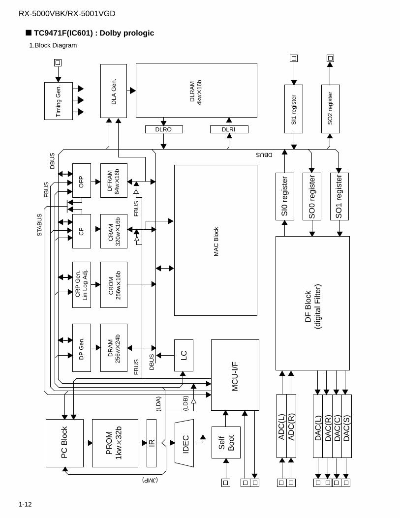
1.Block Diagram
Tim
ing
Gen
.
DLA
Gen
.
DLR
AM
4kw
16
b
DLRO DLRI
SI1
reg
iste
r
SO
2 re
gist
er
DBUS
DB
US
C
RA
M32
0w
16b
OF
PC
P
DF
RA
M64
w
16b
CR
P G
en.
Lin
Log
Adj
.
C
RO
M25
6w
16b
DP
Gen
.
D
RA
M25
6w
24b
FB
US
DB
US
FB
US
MA
C B
lock
SI0
reg
iste
r
SO
0 re
gist
er
SO
1 re
gist
er
DF
Blo
ck(d
igita
l Filt
er)
MC
U-I
/F
AD
C(L
)A
DC
(R)
DA
C(L
)D
AC
(R)
DA
C(C
)D
AC
(S)
Sel
fB
oot
IDE
CLC
IR
PR
OM
1kw
32
b
PC
Blo
ck
(JMP)
(LD
A)
(LD
B)
STA
BU
SF
BU
S
TC9471F(IC601) : Dolby prologic
RX-5000VBK/RX-5001VGD
1-13
123456789101112131415161718192021222324
25~29303132
33~4344
45.4647
48~5354555657
ECKOECKI
A.GNDA.GNDLchOUTV-REF1
A.5VA.5V
V-REF2RchOUTA.GNDA.GND
N.CCchOUTV-REF3
A.5VVROVRIA.5V
V-REF4SchOUT
NCA.GNDD.GND
NCD.5VD.5V
D.GNDNC
D.GNDNC
D.5VNC
RESET
Non connectAmplifier input terminal for external clock input.Ground terminal.(For crystal oscillator circuit)Ground terminal.(For DAC L channel)DAC analog signal output terminal.(L channel)Reference voltage terminal.(For DAC L channel)Power supply terminal.(For DAC L channel)Power supply terminal.(For DAC R channel)Reference voltage terminal.(For DAC R channel)DAC analog signal output terminal.(R channel)Ground terminal.(For DAC R channel)Ground terminal.(For DAC C channel)DAC analog signal output terminal.(C channel)DAC analog signal output terminal with attenuator.(For C channel)Reference voltage terminal.(For DAC C channel)Power supply terminal.(For DAC C channel)Reference voltage terminal for attenuator.(Output buffer)Reference voltage terminal for attenuator.(Input buffer)Power supply terminal.(For DAC S channel)Reference voltage terminal.(For DAC S channel)DAC analog signal output terminal with attenuator.(For S channel)Non connect.Ground terminal.(For DAC S channel)Ground terminal.Non connect.Power supply terminal.Power supply terminal.(For DLRAM)Ground terminal.(For DLRAM)Non connect.Ground terminal.Non connect.Power supply terminal.Non connect.Ground terminal.Power supply.Ground terminal.Power supply.
-I--O----O--OO--OI--O---------------I
Pin No. Symbol I/O Function
2.Pin Function (1/2)

RX-5000VBK/RX-5001VGD
1-14
5859~71
727374
75
7677787980
81,8283
84~8788899091
92,939495
96,979899100
D.5V
DSP-CSDSP-CLKDATA-IN
DATA-OUT
DSP-IFOKDSP-ACKDSP-ERR
I2CSBOOT
D.5V
D.GNDA.GNDLchIN
V-REF5A.5V
V-REF6RchINA.GND
XIXO
A.5V
Pin No. Symbol I/O Function
Power supply terminalNon connect.Chip select signal input terminal.(MCU interface)Data sift clock input terminal.(MCU interface)Data input terminal.(MCU interface)At the IC bus mode,data input /output terminal.Data output terminal.(MCU interface)At the IC bus mode,normally open.Operation flag output terminal.(MCU interface)Acknowledge signal output terminal.(MCU interface)Error flag output terminal.(MCU interface)IC bus mode select terminal.Self-boot control terminal.Non connect.Power supply terminal.Ground terminal.Digital ground terminal.(For ADC L channel)Analog ground terminal.(For ADC L channel)ADC analog signal input terminal.(L channel)Reference voltage terminal.(For ADC L channel)Analog power supply terminal.Reference voltage terminal.(For ADC R channel)ADC analog signal input terminal.(R channel)Analog ground terminal.(For ADC R channel)Crystal oscillator connection terminal.(input)Crystal oscillator connection terminal.(output)Power supply terminal.(For crystal oscillator circuit)
--II
I/O
O
OOOII
----I-----IO-
2.Pin Function (2/2)

RX-5000VBK/RX-5001VGD
1-15
Internal connections for FL display tubeQLF0002-001(DI401):FL DISPLAY TUBE

Printed in Japan200011(V)
VICTOR COMPANY OF JAPAN, LIMITEDAUDIO & COMMUNICATION BUSINESS DIVISIONPERSONAL & MOBILE NETWORK BUSINESS UNIT. 10-1,1Chome,Ohwatari-machi,maebashi-city,371-8543,Japan
No.20883
RX-5000VBKRX-5001VGD