1080p DLP™ LCD - Diagramas dediagramas.diagramasde.com/otros/LCD2005-2006_PTV_Training_Manu… ·...
72
T 2005 2006 ECHNICAL RAINING Projection Television Training Manual Including… Down-to-1 High Speed Troubleshooting COPYRIGHT © 2005 MITSUBISHI DIGITAL ELECTRONICS AMERICA, INC. ALL RIGHTS RESERVED 1080p DLP™ 720p LCD WD-52527 WD-52528 WD-62527 WD-62528 V28 V29 WD-52627 WD-62628 WD-52628 WD-62827 WD-73727 WD-62628 WD-73827 V31 WD-62927 WD-73927 V30
Transcript of 1080p DLP™ LCD - Diagramas dediagramas.diagramasde.com/otros/LCD2005-2006_PTV_Training_Manu… ·...

T 20052006
ECHNICALRAINING
Projection TelevisionTraining ManualIncluding…
Down-to-1High Speed Troubleshooting
COPYRIGHT © 2005 MITSUBISHI DIGITAL ELECTRONICS AMERICA, INC.ALL RIGHTS RESERVED
1080pDLP™
720pLCD
WD-52527 WD-52528WD-62527 WD-62528
V28V29WD-52627WD-62628
WD-52628 WD-62827 WD-73727WD-62628 WD-73827
V31WD-62927WD-73927
V30


I
IntroductionAbout Mitsubishi Electric US ................................................................................. 1
Chapter 1... Display Technologies and PTV Product LineDisplay Technologies ......................................................................................... 1-1PTV Product Line............................................................................................... 1-3
Chapter 2... Disassembly and ServiceEngines ............................................................................................................ 2-1Identification ....................................................................................................... 2-4Chassis ............................................................................................................ 2-4PWBs ............................................................................................................ 2-5Mirror Access..................................................................................................... 2-7LCD Access for Cleaning ................................................................................... 2-8
Chapter 3... Alignment ProceduresOption Menu ...................................................................................................... 3-1Service Mode .................................................................................................... 3-1Mechanical Adjustments ..................................................................................... 3-2Electrical Adjustments ........................................................................................ 3-8
Chapter 4... Down-to-1 TroubleshootingFront Panel LEDs .............................................................................................. 4-1Self Diagnostics................................................................................................. 4-2Interface Troubleshooting ................................................................................... 4-3Symptom/Cause Troubleshooting....................................................................... 4-4
Chapter 5... Circuit Block DiagramsPower Supplies ................................................................................................. 5-1Video Signal Path ............................................................................................ 5-11Sound Signal Path ........................................................................................... 5-15Control Circuitry ............................................................................................... 5-16Lamp Control Circuitry ..................................................................................... 5-17Protection Circuitry........................................................................................... 5-18
2005-2006 PROJECTION TELEVISION TECHNICAL TRAINING AND TROUBLESHOOTING MANUAL
TABLE of CONTENTS

II

1
IntroductionAbout Mitsubishi Electric US Companies
Mitsubishi Electric US markets an extensive line of consumer, commercial and industrial electrical and electronicsproducts. Mitsubishi Electric has more than 2,000 employees in 30 locations throughout the USA.www.MitsubishiElectric.com
Mitsubishi Digital Electronics America, Inc.Mitsubishi Digital Electronics America, Inc. (MDEA)manufactures and markets a premium line of high defini-tion, microdisplay, projection, plasma and LCD flat paneltelevisions and displays; advanced video products suchas DVD and digital VHS components; presentationproducts and projectors; dye sublimation printers; medi-cal and time-lapse VCRs; security digital video record-ers; and photo kiosks. www.mitsubishi-tv.com
Elevator & Escalator DivisionMitsubishi Electric’s Elevator & Escalator Division mar-kets and services elevators and escalators throughoutthe United States. The division designs and installs pre-mier vertical transportation systems, including high-speedelevators and the world’s only spiral escalators.www.MitsubishiElectric.com
Heating, Ventilation & Air Conditioning DivisionMitsubishi Electric HVAC Advanced Products Divisionoffers Mr. Slim split-ductless air conditioners; CITYMULTI, an inverter technology-driven simultaneouscooling and heating system; PlasmaPure room air puri-fication systems; and Jet Towel hand dryers.www.MitsubishiElectric.com/hvac
Semiconductor DivisionMitsubishi Electric’s Semiconductor Division marketsadvanced digital and mixed-signal products that pro-vide unmatched flexibility, design reuse, innovative pack-aging options, ultra-low power and proven high qualityacross a wide range of technologies.www.mitsubishichips.com.
Mitsubishi Electric Automotive America, Inc.Mitsubishi Electric Automotive America (MEAA) of-fers all aspects of engineering, manufacturing, sales andmarketing, distribution and service of electrical and elec-tronic systems and components for automobile manu-facturers and industrial engine manufacturers.www.meaa-mea.com
Mitsubishi Electric Automation, Inc.Mitsubishi Electric Automation, Inc. (MEAU) is a sup-plier of factory automation solutions that include auto-mation platforms; programmable logic controllers; hu-man machine interfaces; programming and control soft-ware; industrial computers; variable frequency drives,servo motors and amplifiers; motion controllers; com-puter numerical controllers; robots; uninterruptible powersupplies; and industrial sewing equipment.www.meau.com
Mitsubishi Electric Power Products, Inc.Mitsubishi Electric Power Products, Inc. (MEPPI) isresponsible for serving the North American electric util-ity, rail transportation, and water treatment industries withelectrical and electronic products, systems and services.MEPPI also provides equipment and services for broad-band over powerline systems.www.meppi.comWithin MEPPI is the Diamond Vision Division, whichmarkets and installs large-scale video displays for sta-diums and arenas, as well as LED displays for indoorand outdoor applications.www.diamond-vision.com

2
Automation Products• Computer Numerical Controllers• Industrial Sewing Equipment• Motion Control Systems• Programmable Logic Controllers• Uninterruptible Power Supplies• Variable Frequency Drives Human-Machine
Interfaces
Automotive Equipment• Automotive Electronics & Sensors• In-car Entertainment Systems• Ignition Coils• Starters• Alternators• ITS Components• Vehicle Navigation & Safety Systems
Elevators and Escalators• Elevators Escalators Maintenance & Refurbish-
ing
Heating and Air Conditioning• Mr Slim & CITY MULTI Climate Control
Systems• PlasmaPure Air Purifiers Jet Towel Hand
Dryers• Compressors
Semiconductors•Optoelectronic, Microwave/RF Semiconductors
Mitsubishi Electric US Products & Services
Home Theater, Presentation & Imaging Products• High Definition TVs• LCD Projectors• Big Screen TVs• Plasma & LCD Displays• DVD & VCR Players• DataWalls• Dye Sublimation & Thermal Imaging Printers• Time Lapse Recorders• Photo Kiosks
Power Products• Broadband Over Power Line (BPL)• Custom & Industrial Power Systems• Flexible AC Transmission• Gas Circuit Breakers• Gas Insulated Substations• Large Power Transformers• Ozone Water Treatment Systems• Rail Transportation Systems• Surge Arresters
Large Screen Displays• Stadium & Arena Displays• Scoreboards LED Signs
Other Technologies• PhotoVoltaic Power Systems• Car Vision Systems

1-1
Display TechnologiesMitsubishi’s Digital Television Product Line for 2005-2006 consists of several different display technologies.They are categorized as either Rear Projection or Di-rect View.Rear Projection Television Technologies:
• CRT• LCD• DLP™• LCoS
Direct View Television Technologies:• Plasma• LCD
This training manual is directed towards Projection Tele-vision technologies.
Each technology offers its own strengths and weak-nesses. Otherwise, only one type would need to be madeavailable. Understanding the differences in each tech-nology will aid the technician when discussing a givenset’s performance with a consumer. Tables 1-1 and 1-2 outline some of the strengths and weaknesses of eachone. Of course, the strengths and weaknesses will changeas each technology evolves over time.
CRT Technology - V27 ChassisThis is the most mature technology of the four. It mayeven be viewed as somewhat “low tech” by somepeople. However, Mitsubishi’s product line includes allthe latest digital features. As such, it can still offer thebest “bang for the buck” of all the technologies. TheV27 Chassis is used in 55”, 65” and 73” models.
LCD Technology - V28 ChassisWhile LCD projection television is certainly not new,recent strides have improved this technology so that Mit-subishi can offer it in 4 models this year.
DLP Technology - V29/V30/V31 ChassisMitsubishi, the first to bring DLP technology to marketin a rear projection television, marks another “first” byintroducing 1080p DLP in 9 different rear projectionmodels. This is twice the resolution of High Definition.It will come in 52, 62 and 73 inch screen sizes, with the73 inch models being the largest DLP models ever avail-able.
LCoSMitsubishi’s use of LCoS technology is in the form of a3 chip system carried over in the 82” rear projectionmodel WL-82913.
CRT LCD DLP LCoSExcellent Color Excellent Color Excellent Color Excellent ColorExcellent Contrast Improving Contrast Excellent Contrast Excellent ContrastRelatively Inexpensive Relatively Inexpensive Cost Improving Excellent Resolution
Light weight Light weightShallow depth Shallow depth
CRT LCD DLP LCoSHeavy Screen Door Potential for Fairly ExpensiveDeep Cabinet Effect Rainbow Effect Limited AvailabilityPotential for Slower refresh ratesPhosphor Burn
Table 1-1: Rear Projection Television Strengths
Table 1-2: Rear Projection Television Weaknesses
Chapter 1Display Technologies & PTV Product Line

1-2
Light EnginesThe CRT technology used in the V27 chassis is electri-cally the same as the V25 chassis. Since the V25 Train-ing Manual covers it in-depth, no further discussion willbe necessary.
LCD, DLP and LCoS are known as “Micro-Display”technologies. The Light Engines are configured differ-ently for each.
LCD uses the “light transmissive” method of producinga picture as light passes through the panel. DLP andLCoS use the “light reflective” method of producing a
Figure 1-1: LCD Light Engine
picture as light reflects off the surface of the display de-vice.
An LCD must use 3 devices to produce a color picture.DLP and LCoS can be configured as either single, or 3device engines. Mitsubishi currently uses a single chipDLP and a 3 chip LCoS system.
The LCD Light Engine, shown in Figure 1-1, uses 3LCD “Panels” to individually produce the red, greenand blue elements of the picture. Dichroic mirrors sepa-rate the red, green and blue elements of light, and an X-Prism is used to re-combine the 3 colors after the pic-tures have been produced.
ProjectionLens
Mirror
Red Blue
XPrism
DichroicMirror
Green
DichroicMirror
LensLens
Lens
Mirror
MirrorLamp
LCD
LCDLCD

1-3
Figure 1-2: DLP Light Engine
ProjectionLens
ShapingLens
Lamp
Condensing Lens RelayLens
DMD
TIRPrism
Color Wheel
The single device DLP Light Engine, shown in Figure1-2, produces a color picture using a color wheel andthe “field sequential” method of displaying the red, greenand blue elements of the picture.
Figure 1-3 shows an LCoS engine in a 3 chip arrange-ment. Like LCD, it produces each color individually.And like DLP, it uses reflective light to produce the pic-ture.
Figure 1-3: LCoS Light Engine
LCoS
ProjectionLens
LCoS
LCoS
Lamp
Mirror
Mirror Red
BlueTIR
Prism
TIRPrism
DichroicMirror
DichroicPrism
TIRPrism
XPrism
Green

1-4
Performance ImprovementTechnologies
The 2005-2006 PTV product line uses several newperformance improvement technologies for LCD andDLP displays.LCD Improvements:
• Quick Motion™• SmartShutter™
DLP Improvements:• 1080p• Dark Detailer™• 10,800 RPM Color Wheel
Quick Motion™ is an advanced high speed drive sys-tem that derives faster response from LCDs, virtuallyeliminating the blurs that often occur when the movingpicture has fast motion.
SmartShutter™ is a dynamic aperture system that im-proves black levels and adds a large palette of darkgrey shades. It does this by reducing light output duringdark scenes without negatively affecting other picturecharacteristics.
Shown in Figure 1-4, the SmartShutter High ContrastUnit (HCU) is located in the light path between the lampoutput and the optics.
The HCU is a motor driven device that dims the lampoutput by physically blocking it with movable louvers.See Figure 1-5. As dark scenes are detected, the lou-vers move from position A, full light output, throughpositions B, C and D to accurately control the amountof light necessary as the picture brightness varies. It iscontrolled by the PWB-Motor Driver.
Figure 1-4: Smart Shutter Location in LCD Light Engine
SmartShutterHigh Contrast Unit
(HCU)
SmartShutterControl PWB
FanLCDDrivePWB
ProjectionLens
Lamp
1-5
Motor
Louvers
Motor
Louvers
A
B
CDLighting
Area
A
B
CDLighting
Area
Figure 1-5: Smart Shutter High Contrast Unit
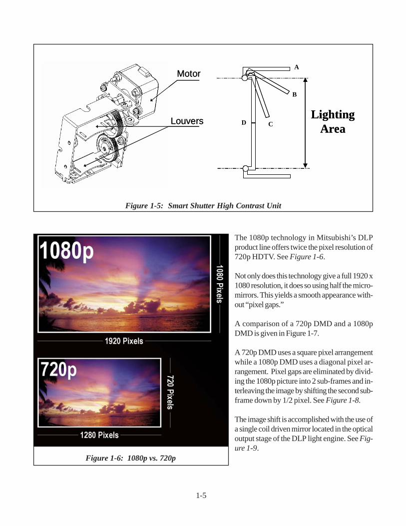
The 1080p technology in Mitsubishi’s DLPproduct line offers twice the pixel resolution of720p HDTV. See Figure 1-6.
Not only does this technology give a full 1920 x1080 resolution, it does so using half the micro-mirrors. This yields a smooth appearance with-out “pixel gaps.”
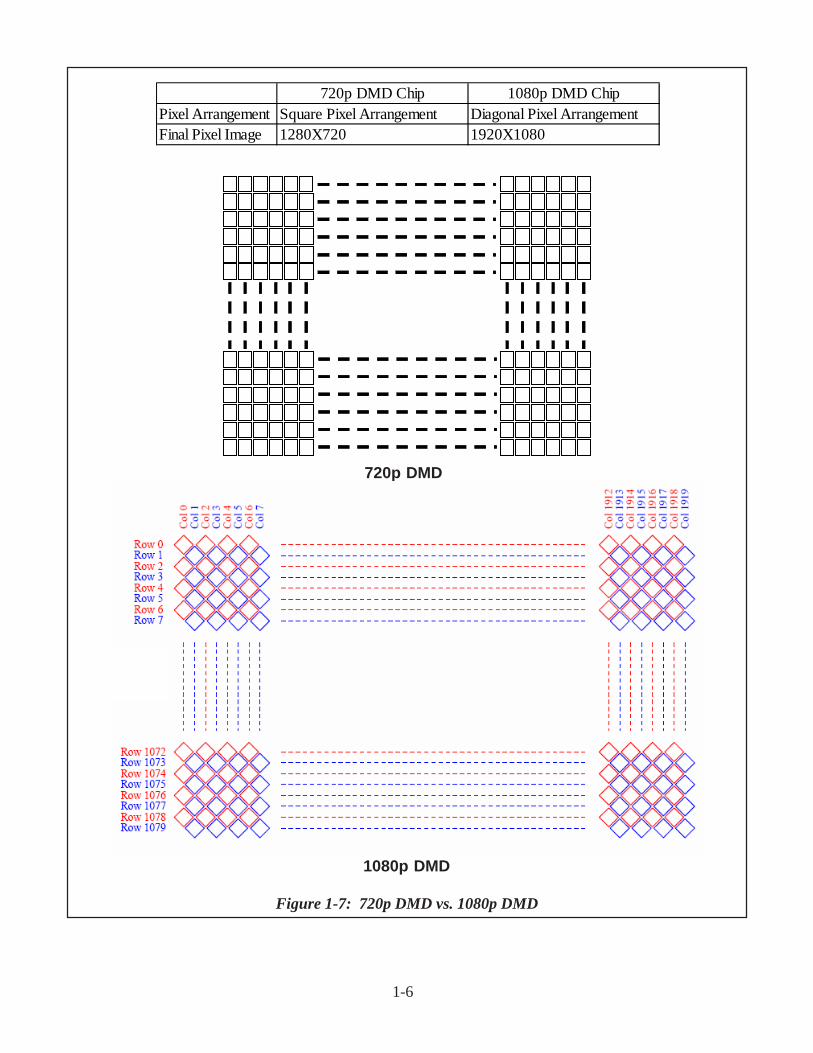
A comparison of a 720p DMD and a 1080pDMD is given in Figure 1-7.
A 720p DMD uses a square pixel arrangementwhile a 1080p DMD uses a diagonal pixel ar-rangement. Pixel gaps are eliminated by divid-ing the 1080p picture into 2 sub-frames and in-terleaving the image by shifting the second sub-frame down by 1/2 pixel. See Figure 1-8.
The image shift is accomplished with the use ofa single coil driven mirror located in the opticaloutput stage of the DLP light engine. See Fig-ure 1-9.
Figure 1-6: 1080p vs. 720p
1-6
Figure 1-7: 720p DMD vs. 1080p DMD
Pixel Arrangement Square Pixel Arrangement Diagonal Pixel ArrangementFinal Pixel Image 1280X720 1920X1080
720p DMD Chip 1080p DMD Chip
720p DMD
1080p DMD

1-7
Figure 1-8: Sub-frame Integration
The data is divided into two subframes, each with half the original data. During one of thesubframes, the image is shifted down by 1/2 pixel. The eye integrates the two consecutivesubframes to create the final image. This process is completd every 1/60 of a second, dis-playing all of the data, every frame, just as is the case for other traditional DMDs.
The resulting image exhibits the same pixel resolution as the original input data in both hori-zontal and vertical directions, using half the number of mirrors. The gaps are also minimizedin the process, resulting in an image that is not only full resolution, but smooth in appearance -without the typical pixel gaps.

1-8
Figure 1-9: DLP Light Engine - 1080p and Dark Detailer Modules
Dark Detailer™ is another type of dynamic aperturesystem used with DLP based models. It displays deeperblacks and better dark scene detail.
The location of the Dark Detailer, also referred to as theDynamic Black (DB) module, is shown with its coverremoved in Figure 1-9. It is located in the light pathbetween the lamp and DLP optics.
Figure 1-10 shows the DB module after it has been re-moved from the engine. The light shutter can be seen atthe top of the picture. It moves into and out of the lightpath to reduce the lamp output during dark scenes. Anaperture opening in the shutter can also be seen.
Figure 1-11 depicts how the one-sided aperture systemprovides the best reliability along with better contrastand uniformity over the entire TV picture.
1080p Module Dark DetailerDynamic Black(DB) Module
Figure 1-10: Dark Detailer Module

1-9
Figure 1-11: One Sided Dynamic Aperture
Because some people can experience a “rainbow ef-fect” due to differences in their persistence of vision, a10,800 RPM Color Wheel is now used in the 2005-2006 DLP product line. This represents a 50% speedincrease over last years 7,200 RPM wheel.
Service TechnologiesThe 2005-2006 PTV product line carries several tech-nologies that affect service. They are:
• PWBs are constructed with Lead Free Solder.• Mirror area is easier to access on 52” LCD &
all DLP to simplify cleaning.• Elimination of ribbon cables in the Electrical
Chassis improves reliability.
• The Interface PWB between the Chassis andLight Engine is convenient for troubleshooting.
• Access to the Electrical Chassis is improved fortroubleshooting and PWB replacement.
• LED diagnostics have been expanded tosimplify troubleshooting.
These topics will be discussed further in this manual.
2005-2006 PTV Product LineSpecifications for the 2005-2006 PTV product line aregiven starting on the following page.

1-10
V27 Chassis

1-11
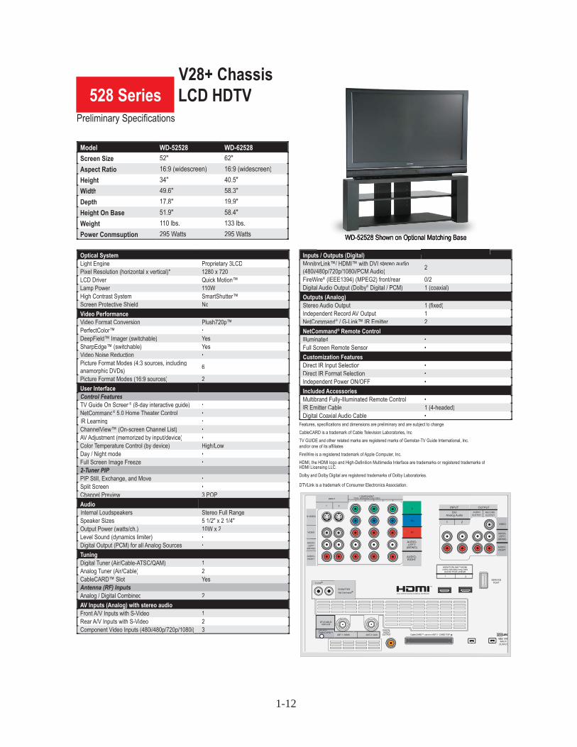
V28 Chassis
1-12
V28+ Chassis

1-13
V29 Chassis

1-14
V30 Chassis

1-15
V30 Chassis

1-16
V30+ Chassis

1-17
V31 Chassis

1-18

FAN-PLATE
LAMP-FAN
LAMP-FANBRACKET INTAKE
COVER
LIGHTENGINE
PWBINTERFACE
ENGINE-PLATE
BALLAST COVER& BALLAST
V28 / V28+ LCD Optical Engine
2
Chapter 2Disassembly and Service
2-1

(View from back)Ballast Fan
Ballast Cover
Lamp Cartridge
Interface PWB
Engine PWR PWB
Ballast Plate
Lamp Duct Lens Cushion(View from front)
Engine Plate
Bottom Plate
Lamp Fan(120W Version) (note on 150W version
Lamp Fan is in front)
V29 / V30 / V30+ / V31 DLP Optical Engine
Wedge locationUsed on 52” and 62” modelsafter adjustment/before locking
2-2

After engine has been installed the engine dataneeds to be copied to the chassis.
Press MENU + 2457 + 0Press ENTER to select copy light engineEEPROM to DM
From replacement engine:Remove Lens Cap and install tooriginal engine.Remove 2 protective foampieces and install to originalengine for shipping.
V28 engine picutred. V29-V31engines also require lens cap butdo not have protective foam.
Engine replacement instructions are included in the applicable service manuals aswell as being included with the replacement part when it is shipped.
2 Protective Foam pieces
Lens Cap
ENGINE DATA COPY (V29/30/31 Only)
ENGINE SHIPPING PREP
V28 ENGINE SHUTTER (Contrast control system)
LCD engine has a contrast control shutter unit. If this unit is notfunctioning the TV may not turn on. Error code can report “5-6”,you may want to check CN5.
2-3
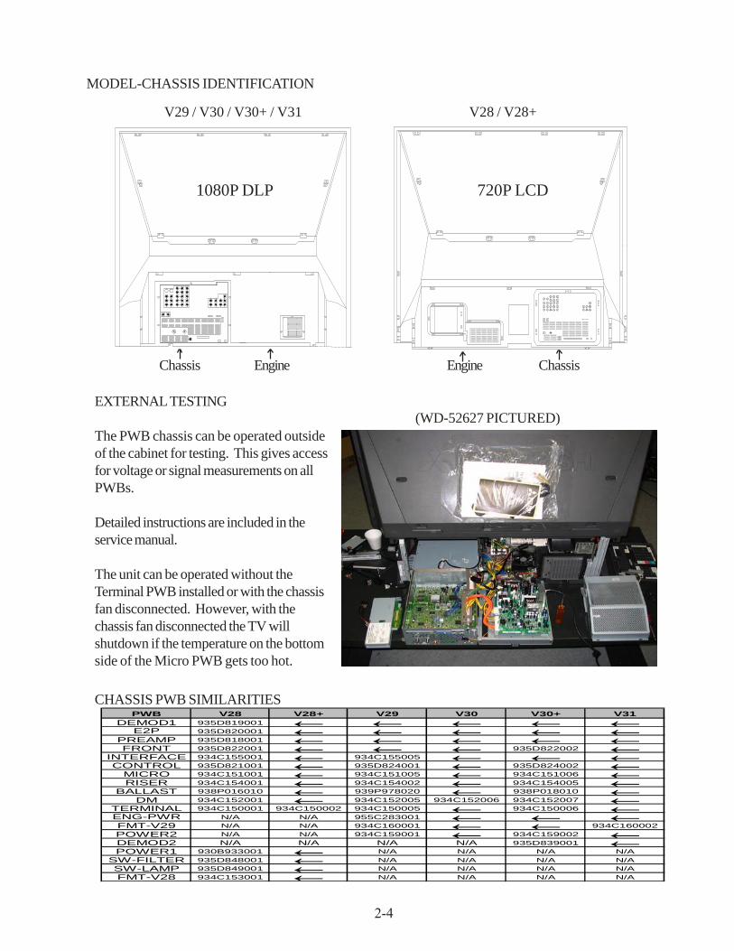
Chassis Engine
1080P DLP
V29 / V30 / V30+ / V31
ChassisEngine
720P LCD
V28 / V28+
MODEL-CHASSIS IDENTIFICATION
(WD-52627 PICTURED)EXTERNAL TESTING
The PWB chassis can be operated outsideof the cabinet for testing. This gives accessfor voltage or signal measurements on allPWBs.
Detailed instructions are included in theservice manual.
The unit can be operated without theTerminal PWB installed or with the chassisfan disconnected. However, with thechassis fan disconnected the TV willshutdown if the temperature on the bottomside of the Micro PWB gets too hot.
CHASSIS PWB SIMILARITIESPWB V28 V28+ V29 V30 V30+ V31
DEMOD1 935D819001 ← ← ← ← ←E2P 935D820001 ← ← ← ← ←PREAMP 935D818001 ← ← ← ← ←FRONT 935D822001 ← ← ← 935D822002 ←
INTERFACE 934C155001 ← 934C155005 ← ← ←CONTROL 935D821001 ← 935D824001 ← 935D824002 ←
MICRO 934C151001 ← 934C151005 ← 934C151006 ←RISER 934C154001 ← 934C154002 ← 934C154005 ←
BALLAST 938P016010 ← 939P978020 ← 938P018010 ←DM 934C152001 ← 934C152005 934C152006 934C152007 ←
TERMINAL 934C150001 934C150002 934C150005 ← 934C150006 ←ENG-PWR N/A N/A 955C283001 ← ← ←FMT-V29 N/A N/A 934C160001 ← ← 934C160002POWER2 N/A N/A 934C159001 ← 934C159002 ←DEMOD2 N/A N/A N/A N/A 935D839001 ←POWER1 930B933001 ← N/A N/A N/A N/A
SW-FILTER 935D848001 ← N/A N/A N/A N/ASW-LAMP 935D849001 ← N/A N/A N/A N/AFMT-V28 934C153001 ← N/A N/A N/A N/A
2-4

DM PWB
DEMOD1 PWB
DEMOD2 PWB
E2P PWB
PWB LOCATIONS
POWER PWB
RISER PWB
MICRO PWB
FMT PWB
2-5
RHS6352
Text Box
TERMINAL-PWB
RHS6352
Line
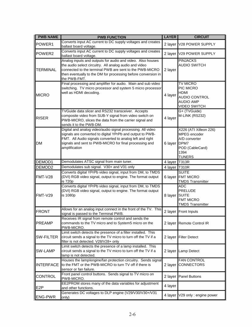
PWB NAME PWB FUNCTION LAYER CIRCUIT
POWER1 Converts input AC current to DC supply voltages and creates ballast board voltage. 2 layer V28 POWER SUPPLY
POWER2 Converts input AC current to DC supply voltages and creates ballast board voltage. 2 layer V29 POWER SUPPLY
TERMINAL
Analog inputs and outputs for audio and video. Also houses the audio select circuitry. All analog audio and video connected to the terminal PWB are sent to the PWB-MICRO then eventually to the DM for processing before conversion in the PWB-FMT.
2 layer
PINJACKSAUDIO SWITCH
MICRO
Final processing and amplifier for audio. Main and sub video switching. TV micro processor and system 5 micro processor well as HDMI decoding. 4 layer
TV MICROPIC MICROHDMIAUDIO CONTROLAUDIO AMP VIDEO SWITCH
RISER
TVGuide data slicer and RS232 transceiver. Accepts composite video from SUB-Y signal from video switch on PWB-MICRO, slices the data from the carrier signal and sends it to the PWB-DM.
4 layer
G+ (TVGuide)M-LINK (RS232)
DM
Digital and analog video/audio signal processing. All video signals are converted to digital YPrPb and output to PWB-FMT. All Audio signals converted to analog left and right signals and sent to PWB-MICRO for final processing and amplification
6 layer
X226 (ATI Xilleon 226) MPEG encoder A/D converter DPM7 POD (CableCard) 1394 TUNERS
DEMOD1 Demodulates ATSC signal from main tuner. 4 layer T313RDEMOD2 Demodulates sub signal. V30+ and V31 only 4 layer T310R
FMT-V28Converts digital YPrPb video signal, input from DM, to TMDS (DVI) RGB video signal, output to engine. The format output is 720p
6 layerSUITE FMT MICRO TMDS Transmitter
FMT-V29
Converts digital YPrPb video signal, input from DM, to TMDS (DVI) RGB video signal, output to engine. The format output is 1080p 8 layer
ADCPRELUDESUITEFMT MICROTMDS Transmitter
FRONT Allows for an analog input connect in the front of the TV. This signal is passed to the Terminal PWB. 2 layer Front Inputs
PREAMPReceives IR signal from remote control and sends the commands to the TV micro and to System5 micro on the PWB-MICRO.
2 layer Remote Control IR
SW-FILTERLimit switch detects the presence of a filter installed. This circuit sends a signal to the TV micro to turn off the TV if a filter is not detected. V28/V28+ only
2 layer Filter Detect
SW-LAMPLimit switch detects the presence of a lamp installed. This circuit sends a signal to the TV micro to turn off the TV if a lamp is not detected.
2 layer Lamp Detect
INTERFACEHouses the lamp/engine/fan protection circuitry. Sends signal to the FMT or the PWB-MICRO to turn TV off if there is sensor or fan failure.
2 layerFAN CONTROLCONNECTORS
CONTROL Front panel control buttons. Sends signal to TV micro on PWB-MICRO. 2 layer Panel Buttons
E2PEE2PROM stores many of the data variables for adjustment and other functions. 4 layer
ENG-PWRGenerates DC voltages to DLP engine (V29/V30/V30+/V31 only) 4 layer V29 only : engine power
2-6

A
MIRROR ACCESSRemove (10) screws maked “A” below for 52” and 62” models and (19) screws maked “A” below for73” models. Panel can then be removed to expose the mirror and inside of the upper cabinet
A
(73” models)
(52” and 62” models)
2-7

LCD ENGINE ACCESS PANEL
Remove (2) screws shown below to gain access to the LCD engine area for cleaning of debris(V28/V28+ only).
(View from Front of unit)
2-8

2-9
Lead Free SolderMitsubishi's 2005-2006 product line, including the V28,V29, V30 and V31 chassis, will be constructed usinglead free solder.
This is the first part of a 3 phase program to eliminatethe lead content in all MDEA's electronic products. The3 phases are:
• Phase 1… PCB's constructed using Pb-freesolder. PCB surface finishing and componentsmay contain Pb.
• Phase 2… Solder, PCB surface finishing andcomponent lead plating is Pb-free. Componentsmay have internal Pb.
• Phase 3… Solder, PCB surface finishing andcomponents are Pb-free. (100% Pb-free)
Pb-Free Phase Definition Display
Short Display (W hen the area is too small)
Phase-1 PCB's constructed using Pb-free solder.
Phase-2 Solder, PCB surface finishing and component lead plating is Pb-free. Components may have internal Pb.
Phase-3 Solder, PCB surface finishing and components are Pb-free. (100% Pb-free)
Table 2-1: Pb-Free Phases and Symbols
Pb PCA
Pb Joints
Pb S
Pb J
Pb P
Pb Solder
Displays used to indicate Pb-freePCBs will be marked, indicating the level of Pb-freeconstruction. Table 2-1 defines the levels by phase andshows the different symbols that will be displayed onthe PCB. Additionally, a PCB constructed using Pb-free solder may be simply marked LFS.
When possible, the indication will be placed close tothe part number that is screened onto the PCB (not thepart label). Figure 2-1 is an example of a PCB show-ing the display and its location.
Pb free solder differs from conventional leaded solder.• The amount of tin in Pb-free solder is greater.• The melting point of Pb-free solder is higher.
Figure 2-1: Pb-Free Display on PCB
Pb-FreeDisplay

2-10
Also, Lead-free solder does not "wet" as well as leadedsolder. That means it has trouble adhering to both thesoldering iron tip and the surface being soldered. Tocounteract this, the flux used is more corrosive. Lead-free solder also does not change from solid to liquid orback again all at once. It passes through a soft state.So, the melting process actually occurs through a rangeof temperatures.
This makes a significant impact when repairing PCBsusing Pb-free solder. Problems that can be encoun-tered working with Pb-free solder are:
• Excessive heat can cause the PCB to warp,detaching surface mount components.
• Excessive heat may cause thermal damage tocomponents.
• Excessive heat can cause plastics such asconnectors, relays, LEDs, electrolytic capaci-tors, etc. to melt or warp.
• Higher temperatures can cause surface oxida-tion resulting in poor solder spread-ability andwet-ability.
• The flux is more corrosive.• The time required for a good solder connection
may be longer.• Poor wet-ability can cause solder balls.• Higher temperatures can cause flux spattering.• Soldering iron tip life is shortened.• Duller finish solder joint can appear to be a
"cold" solder joint.
Pb-free Hand SolderingHand soldering with lead-free solder doesn’t necessar-ily require higher soldering temperatures. The meltingtime will be slightly slower than with leaded solder, re-quiring an increase in contact time. The solder joint willalso look different. It will have a dull finish that is similarin appearance to a "cold" solder connection when usingleaded solder.
To help eliminate problems working with lead free sol-der, consider the following points.
Temperature… Use the same soldering temperatureas you would with tin-lead solder, about 700 F. If hot-ter, you may be making it more difficult to solder. Thehigher temperature causes oxidation to form faster, mak-ing wetting even more difficult. Excessive temperaturescan also lengthen the cooling time, allowing micro-cracksto form within the joint.
Thermal Recovery… Use a soldering iron with goodthermal recovery. When the iron is first applied to acool joint, the heat transfer causes the tip temperatureto drop. A higher powered iron will bring the tip backup to the proper temperature faster. Using a shorter tipwill also improve thermal recovery.
Thermal Conduction… Use the widest tip possible inrelation to the joint being soldered. This will allow theheat to conduct to the joint better. Also keep the tipwetted for better heat transfer.
Tip Cleanliness… Important! Keep the solderingiron tip clean at all times using a damp sponge. Re-tinthe tip before returning the iron to its stand. To extendthe tip life, do not leave the iron on when it is not beingused for longer periods of time.
De-soldering… For the same reasons as soldering,increasing the temperature for de-soldering is not desir-able. However, if a vacuum de-soldering tool is used,the solder must remain molten from the tip, all the wayto the entrance to the filter. If the solder hardens alongthe way, it can clog the tool.
SolderWhen performing repairs, it is necessary to use solderas that is compatable with that used in the original manu-facture. Leaded solder cannot be used when solderingPCBs manufactured with Pb-free solder. And, Pb-freesolder cannot be used on PCBs manufactured usingleaded solder.
The Mitsubishi standard for service requires the use ofTin-Silver-Copper ( Sn-96.5, Ag-3.0, Cu-0.5) solder.It can be obtained through the Parts Department.Order part number: PB FREE SOLDER

3-1
Option MenuThe Option Menu and Option Menu access is the sameon all chassis. To activate the Option Menu press“MENU-2-4-7-0”. Figure 3-1 shows the OptionMenu.
Service ModeActivation of the Service Mode is also the sameon all chassis, Press “MENU-2-4-5-7”. Theprocedure for using the Service Mode has notchanged:
• “AUDIO” selects a function• “VIDEO” selects a specific adjust-
ment item• “UP & DN’ buttons adjusts data• “ENTER” saves data changes.
There are two Adjustment Function on Eachchassis type.V28 Adjustment Functions
1) AD9881 Sub2) fmt
V29/V30/V30+/V31 Adjustment Functions1) Doubler2) fmt
In either case, only the “fmt” function is used to performservice Adjustments.
Chapter 3Adustments
Data Transfer "MENU-2-4-5-7-0"Display Description
Restore Back Up Resets data to factory valuesUpload Terminal Data Not usedDown load WB data to FMT Use after replacing Engine PWB-FORMAT
Table 3-1: V28 Data Transfer Choices
Data TransferThe data Transfer mode is activated when in the Ser-vice Mode by pressing “0”. Table 3-1 show the DataTransfer choices in the V28 chassis, and Table 3-2 thechoices in the DLP chassis (V29/V30/V30+/V31)
All chassis types can:• Be Reset to Factory values• Down load WB data to the FMT board
Down loading WB (White Balance) data to the FMTboard is necessary if the PWB-FORMAT is replaced.The DLP chassis, “Copy Engine E2PROM data to theDM” is added. This is necessary if the DLP Engine isreplaced.
Figure 3-1: Option Menu

3-2
Service AdjustmentsAdjustments are divided into two categories, mechani-cal and electrical. The Electrical Adjustments are posi-tioning (centering) adjustments and the procedures arethe same on both the LCD and DLP models.
Mechanical AdjustmentsThe Mechanical Adjustments are similar, but differ dueto the different type Light Engines, Adjuster Assembliesand accessing procedures differ.
The Mechanical Adjustments on the V28 chasssis are:• Vertical Keystone Adjusment• Picture Rotation Adjustmennt
On the V29~V31 chassis the Mechanical Adjustmentsare:
• Picture Rotation Adjustment• Horizontal Keystone Adjusments• Vertical Keystone Adjustments.
Adjustment Test PatternFigure 3-2 shows the internal Test Pattern is used on allchassis to perform the adjustments. When adjustmentsare complete press “MENU” twice to
The internal Test Pattern can be activated when in theService Adjustment Mode:
1) Press “MENU-2-4-5-7” in sequence to activatethe Service Mode.
2) Press “REW” while in the Service Mode to acti-vate the Test pattern.
3) When Adjustments are complete press “ENTER”to save and “MENU” twice to exit the ServiceMode.
Red = 4% overscanWhite = 5% overscanGreen = 6% overscanCyan = 7% overscanYellow = 10% overscan
Figure 3-2: Internal Test Pattern
Data Transfer MENU-2-4-5-7-0Display Description
Copy Engine E2PROM to DM Transfers Engine data to DM E2PROMRestore Backup Restores data to factory valuesUPLOAD TERMINAL BOARD DATA DO NOT USEDownload WB Alignment to FMT Transfers Engine data to FMT
Table 3-2: DLP Chassis Data Transfer Choices

3-3
Preliminary(Refer to Figure 3-3)
1) Loosen the Fixing Screw (1) and (2) in theSlide -Lock-Mate.
2) Loosen Nuts (1) and (2) on the Adjuster3) Loosen [A-1] and [A-2] on the Adjuster (4mm
Allen wrench)
V28 Mechanical AdjustmentsIn the V28 chassis, the Mechanical Adjuster is accessedfrom the rear. Refer to the disassembly instructions andremove the BACK-COVER.
Tools Required:• 2mm L shaped Allen wrench• 4mm L shaped Allen wrench• Hex wrench
Figure 3-3: Locking Screws & Nuts

3-4
Keystone Distortion Adjustment(Figure 3-4)
1) Loosen [A-1] and [A-2] so they clear[A-3].
2) For distortion at the top of the picturerotate [A-3] counter-clockwise.
3) For distortion at the bottom of the pic-ture rotate [A-3] clockwise.
After Adjustment1) Tighten Nuts (1) and (2).2) Tighten Slide Lock-Mate screw (1) and (2).3) Insure [A-1] and [A-2] are flush against [A-3
Rotation Adjustment(Figure 3-5)
Clockwise Rotation Needed1) Loosen [A-2].2) Use [A-1] to adjust rotation.
Counter Clockwise Rotation Needed1) Loosen [A-1}.2) Use )A-2] to adjust rotation,
Figure 3-4: Keystone Adjustment
Figure 3-5: Rotation Adjustment

3-5
Test Signal ActivationUse the same procedure as in the V28 chassis.(MENU-2-4-5-7-REW)
Required Tools• 4mm hex wrench (10 inches long mnimum)• 5mm Allen wrench (10 inches long minimum)• 10mm hex or Phillips driver
PrelminaryMechanical Optical Engine Adjustments are made using the UNIT-ADJUSTER shown in Figure 3-6. The UNIT-AD-JUSTER is mounted under the Light Engine on the Engine Plate. It is accessed from the front of the set through theopening for the Card Reader. Refer to the model specific Disassembly Instructions and remove the:
• Back Cover• Speaker Grille• Card Reader
Locking Screws and Wedge RemovalBefore mechanical adjustments can be made, locking screw [B-1]and [B-2] must be loosened.
• [B-1] is located on the front of the UNIT-ADJUSTER,refer to Figure 3-6 and Figure 3-9.
• [B-2] is accessible from the rear of the unit on the right sideof the Optical Engine, refer to Figure 3-7.
• Remove the Rubber Wedge shown in Figure 3-8
NOTE: There is no Wedge used in 73 inch models[B-2]
Figure 3-7: [B-2] Lock ScrewWARNING: DO NOT loosen [B-2]too far. The nut on the other side maydrop off. Then the Optical Engine mustbe removed to re-install the nut.
DLP Chassis Mechanical Adjustments
[A-1]VERT. KEYSTONE
4mm Hex
[B-1]LOCKING SCREW
5mm Allen Wrench
[A-3]HORIZ. KEYSTONE
4mm Hex
[A-2]ROTATION4mm Hex
Figure 3-6: UNIT-ADJUSTER

3-6
Adjustment ProceduresAdjustment LocationsThe Mechanical Adjustment are accessed through thefront opening for the Card Reader. Locations of theadjustments are shown in Figure 3-9
CAUTION: Do Not force an adjustment pastthe end of it’s range, UNIT-ADJUSTER damagemay result.
[B-1]
[A-1]Access
[A-2]
[A-3]
Figure 3-9: Adjustment Locations
Figure 3-8: Rubber Wedge (52 and 62 inch models only)
RUBBERWEDGE

3-7
Rotation AdjustmentAdjust [A-2] to remove any picture rotation
Horizontal Keystone AdjustmentAdjust [A-3] to remove horizontal keystone distortion.NOTE: Vertical Positioning may shift
Vertical Keystone ADjustmentAdjust [A-1- To remove vertical keystone distortion.[A-1] can only be accessed by the front access holeshown above.NOTE: Horizontal Positioning may shift.
After Adjustment1) Slide the rubber wedge under the Engine slowly until it makes solid contact. (Figure 3-8 and Figure 3-11)2) Tighten side locking screw [B-2]. (Figure 3-7)3) Check the picture, re-adjustment may be required (usually Rotation).4) Tighten front locking screw. (Figure 3-9)
RUBBERWEDGE
Figure 3-11: Wedge Insertion
Figure 3-10: Adjustments

3-8
Electrical AdjustmentsThe only Servicer electrical adjustments are picture position (centering). These adjustments are the same on allchassis (V28 / V29 / V30 / V30+ / V31). They are also the same as last years DLP models. They are repeated hereas a reference.
Horizontal & Vertical Positioning1) Press “MENU-2-4-5-7”, activates the Service Mode..2) Select the “FORMAT” function (AUDIO button).3) Press “REWIND”, activates the Overscan Test Pattern4) Select “Item 1” HPOS (VIDEO button).5) Use the ADJUST buttons to center the picture horizontally.6) Press ENTER to save the new setting.7) Select “Item 2” VPOS (VIDEO button).8) Use the ADJUST buttons to center the picture vertically.9) Press ENTER to save the new setting.
10) Press MENU to exit the Service Mode.

4-1
Chapter 4Down-to-1 Troubleshooting
The goal of Down-to-1 troubleshooting is… using aminimum amount of time and test equipment, makean accurate diagnosis of a failure 9 out of 10 times.The 2005-2006 Micro-Display product line lends itselfto this discipline very well.
Using The Front Panel LEDsThe front panel LEDs, Figure 4-1, provide an indica-tion of the sets operation, and the possible cause of amalfunction. There are three front panel LEDs, “Power”,“Status” and “Lamp”. Which LED is lit, the color andwhether it is blinking or steady indicates to the customerthe current status, or a possible malfunction. Using theFront Panel LEDs is similar for LCD and DLP basedsets. The indications are also listed in the Owners Guide.
Figure 4-1: Front Panel LEDs
Normal Indications… The LEDs provide the cus-tomer with status information that indicates several nor-mal operational modes. Normal indications are give inTable 4-1.
Abnormal Indications… The LEDs also provide thecustomer with status information indicating abnormal con-ditions. Abnormal indications are give in Table 4-2.
POWER LED
STATUS LED
LAMP LED
Power Status Condition
Off Off Off Stby OffGreen Off Off P-0N Power On
Off Off Blinks Green
30 Seconds After Off
Set cannot be turned On until Lamp has cooled.
Blinks Green Off Off Stby Booting after AC applied
Slow Blinks Green Off Off Stby On Timer is set
POWER LED
STATUS LED
LAMP LED
Power Status Condition
Off Yellow Off Low Power Excess Temperature
Off or On Off Yellow No change Lamp time over 4000 Hrs.
Off Off Blinks Yellow
Low Power Lamp Cover open
Off Blinks Yellow Off " Filter Cover Open (V28 Only)
Off Off Red Stby Lamp did not turn On
Off Blinks Red Off Low
Power Fan Stopped
Off Red Off " Circuit Failure
Normal LED Indications
Abnormal LED Indications
Table 4-1
Table 4-2

4-2
Self Diagnostics…When an abnormal condition is in-dicated by the front panel LEDs. Or, when the TV turnsOn and then shuts Off, the Self Diagnostics help isolatethe problem. This is similar to the Self Diagnostic fea-ture on previous model TVs. For both the V28 andV29/30/31 Chassis, it has been greatly expanded.
The Self Diagnostics activation procedure is describedas follows:
1) With the TV Off2) Press and hold the front panel "MENU" and
"DEVICE" buttons for 5 seconds.3) The LED will flash the Error Code indicating
what caused the TV to shut Off.4) The Error Code will be repeated 5 times.
When the LED stops flashing, the mode isautomatically terminated.
Error Code Description12 No error detected32 Lamp Cover open33 Air Filter Cover open34 Lamp abnormality35 DM Fan failure36 Exhaust or Lamp Ballast Fan failure37 LCD Engine Fan failure38 Lamp temperature abnormally high39 LCD temperature abnormally high41 Short is detected42 Lamp Fan failure44 DVI cable between Format and Engine disconnected45 Shutter (PBS) Fan Failed46 JC connector disconnected47 DM Temperature too high48 Engine power supply short detected51 Speaker short detected56 Shutter not connected
Error Code Description
12 No error detected32 Lamp Cover open34 Lamp abnormality35 DM Fan failed (Chassis Fan)36 Exhaust or Lamp Ballast Fan failure37 DMD Engine Fan failure38 Lamp temperature abnormally high39 DMD temperature abnormally high41 Short is detected (Standby Power Supplies)42 Lamp Fan failure44 DVI cable between Format and Engine disconnected46 DMD Fan failed (JC connector disconnected)47 DM Temperature too high48 Engine power supply short detected51 Speaker short detected52 HDD excess temperature (V30+ & V31 only)55 HDD Fan Stopped (V30+ & V31 onlyt)
Table 4-3: Error Codes
V28 ERROR CODES
V29/V30/V31 ERROR CODES
Reading the Error CodesThe Error Codes are two digit numbers. The LED:
• Flashes the value of the most signifi-cant digit (MSD).
• Then there is a pause.• Flashes the value of the least signifi-
cant digit (LSD).• The Error Code is repeated 5 times.
Example: If the Error Code is “32”, the LEDwill flash three times, pause, and then flashtwo times then repeat the sequence 5 times.If the technician is still uncertain of the code,repeat the procedure.
After the error code is known, troubleshootthe area indicated. For instance, if excessivetemperature is indicated when the set is knownto be cool, suspect a failed sensor.

4-3
Interface TroubleshootingThe Interface PWB provides the service technician witha convenient test point for many of the peripheral com-ponents such as the Engine, Lamp Circuit, Fans andSensors. It is easily accessible as it is located in thecenter of the set, directly in the rear of both the LCDand DLP models.
Figure 4-2 shows the layout of the Interface for theLCD, V28 Chassis. Figure 4-3 shows the layout forthe DLP, V29/30/31 chassis. These layouts are as thetechnician is viewing the PWB from the rear of the set.
To save time, use the Symptom/Cause information alongwith the Circuit Block Diagrams to make checks on theInterface PWB first.
Figure 4-2: V28 Chassis PWB Interface Layout… As viewed from the rear.
Figure 4-3: V29/30/31 Chassis PWB Interface Layout… As viewed from the rear.
V28
V29/30/31

4-4
Symptom/Cause TroubleshootingUse the following symptom/cause charts to determinethe most likely cause of a failure.
The areas covered are:• PWB Symptom/Cause• Optical Engine
• Power Supply PWB• Micro & Terminal PWB
First use the PWB Symptom Cause chart to narrowdown the problem to a PWB. Then check the connec-tions to the PWB specified. The additional charts canhelp repair the set without ordering a PWB.
Symptom Most Likely Other PossibilityVideo Problems, all Inputs & Menu bad. Audio OK
Reseat DVI Cable between Engine and Chassis
Analog Tuning problems. External Inputs & Digital OK PWB-DM PWB-MICROAnalog Tuning & External Inputs Problems. Digital OK PWB-MICRO PWB-TERMINALDigital Tuning problems. Analog OK PWB-DMAnalog & Digital Tuning Problems. External Inputs OK PWB-DMExternal Input Problems. Tuning OK PWB-TERMINAL PWB-MICRONo Sync PWB-FMTVideo Problems. Digital noise, lines or artifacts in picture PWB-FMT Optical EngineCard Reader Problems Memory Card Reader PWB-DM1394 Problems PWB-DMAudio Problems. Speakers Bad. Analog & Digital Out good PWB-MICROAudio Problems. Speakers, Monitor A/V 1, Audio 2, Digital Out Bad PWB-DMAudio Problems. Digital Good. Analog Bad PWB-TERMINALPower LED blinking constantly. Won't power on. PWB-DMCableCARD problems PWB-DMNetCommand problems PWB-DMControl problems PWB-DMControl problems (Front Panel) PWB-CONTROL PWB-INTERFACEControl problems (Remote) PWB-PREAMP PWB-INTERFACE
PWB Symptom/Cause Troubleshooting

4-5
Symptom Cause What to checkFMT does not turn on lamp due to fault detection
Check error code on front pannel. Check problem indicated.
No DC supply to ballast Check power PWB PL connector for approx. 340VDC. Check connections PL-JE, JE-CN2
No Lamp enable signal Check FMT output Lamplitz FB pin 1. Check connections FB-FB, CJ3-CJ3
Lamp end of life Repace lamp and check Ballast Broken Replace ballast and check
FMT does not turn on video Check diagnostic code. Check circuit indicated.DVI cable not connected check DVI connectionsEngine power missing Check connections PA2-CN102Engine is blanked. Check control connections FC-FC, KC-CN3100.FMT not providing video signal Check FMT Board.Engine broken Replace engine and check.
No power to Shutter Check 18V from Power board PB pin4. Check connections PB-PB, KD-CN1
No control of shutter Check connections CN5-JG, JG-KD, KD-CN2FMT does not control shutter Replace FMT and check.Shutter broken Replace engine.
Fan not working. Temp sensor. Check error code and check indicated fan or sensor.Filter clogged (V28) Check filter and clean or replace.Temp sensor problem Check error code. Check connections DT-KB, LT-KB.
Check sensor Air path blocked Check air flow from each engine fan.
Set Shuts down after
a while
OPTICAL ENGINE TROUBLESHOOTING
No Light
No Picture,
bad picture
High Contrast Unit not W ork ing
(V28)

4-6
POWER PWB TROUBLESHOOTING
SYMPTOM CHECK POINT POSSIBLE CAUSECheck +15VS @ connector PD pin 1 Check Q9E00 circuitCheck -15VS @ connector PD pin 7 Check Q9E00 circuit
Check doubler circuitCheck ballast circuitIC9A24 circuitZener D9A43
Check 18V @ L9A45/C9A82 Q9A13 circuitIC9A23 circuitZener D9A41IC9A21 circuitQ9A12 circuitZener D9A47F9E10F9E11
CHECK ALL FUSEST9A10 circuitIC9A10 circuitIC9A22 circuitZener D9A39
Check connector PD pin 20 for HIGH (active) PC9A21 circuit
NO POWER
Check 340VDC @ connector PL
Check 3.3V @ connector PA2 pin 1
Check 12VS @ connector PD pin 14
Check 5VS @ connector PC pin 8
Check 4.5V @ connector PD pin 19
Check 18V @ TP18VS
Check 5VSL @ connector PD pin 16
ERROR CODE 51
ERROR CODE 34
ERROR CODE 48
ERROR CODE 41
4-7
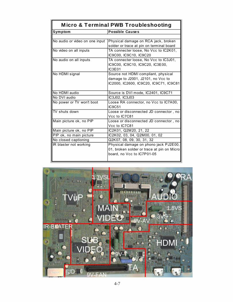
Symptom Possible Causes
No audio or video on one input Physical damage on RCA jack, broken solder or trace at pin on terminal board
No video on all inputs TA connecter loose, No Vcc to IC2K01, IC9C00, IC9C10, IC9C20
No audio on all inputs TA connecter loose, No Vcc to IC3J01, IC9C00, IC9C10, IC9C20, IC3E00, IC3E01
No HDMI signal Source not HDMI compliant, physical damage to J2001, J2101, no Vcc to IC2000, IC2600, IC9C20, IC9C71, IC9C81
No HDMI audio Source is DVI mode, IC2401, IC9C71No DVI audio IC3J02, IC3J03No power or TV won't boot Loose RA connector, no Vcc to IC7A00,
IC9C51TV shuts down Loose or disconnected JD connector , no
Vcc to IC7C81Main picture ok, no PIP Loose or disconnected JD connector , no
Vcc to IC7C81Main picture ok, no PIP IC2K01, Q2M20, 21, 22PIP ok, no main picture IC2K02, 03, 04, Q2M00, 01, 02No closed captioning Q2K07, 08, 09, 30, 31, 32IR blaster not working Physical damage on phono jack PJ2E00,
01, broken solder or trace at pin on Micro board, no Vcc to IC7P01-05
M icro & Terminal PWB Troubleshooting

4-8

5-1
Chapter 5Block Diagrams & Signal Path
Power SuppliesAlthough the LCD Light Engine models (V28 chassis)and DLP Light Engine models (V29, V30, V30+,V31)are different, a large part of the circuitry is the same orvery similar in all chassis types.
The material in this chapter covers differences in cir-cuitry between the LCD and DLP chassis. Sincetroubleshooting will be mainly to board level, the PowerSupplies, Signal Path and Control circuitry connectionsand paths between the various PWBs is also described.
The simplified Block Diagrams should help in isolatingproblems to a specific PWB.
Power Supply Basic DescriptionFigure 5-1 shows the Basic Power Supply that is thebasis for all the chassis types. The Main Power Supplyis on PWB-POWER. The main Standby, Switched andBallast DC supplies are generated on the PWB-POWER. It is also the source for the Fan Power Sup-plies located on the PWB-INTERFACE.
On the DLP chassis, a PWB-ENG-PWR board isadded. This board generates the DC supplies requiredby the DLP Engine.
In the V30+ and V31 chassis models, a Hard Disc Drive(HDD) has been added. The additional Power Supply
Figure 5-1: Basic Power Supply Block Diagram

5-2
for the HDD is located on the PWB-POWER for thesetwo chassis types.
Due to differences between the various chassis thereare three version of the PWB-POWER. These are listedin Table 5-1.
Switch Mode RegulatorThe Switch Mode Regulator (SMR) on the PWB-POWER is the initial source for all DC Supplies exceptthe DC supply for the Ballast.
Figure 5-2 shows a simplified diagram of the SwitchMode Regulator. This circuitry is conventional and is
Figure 5-2: Switch Mod Regulator
PWB Part Number Models
ASSY-PWB-POWER1 930B933001 All V28 models
ASSY-PWB-POWER2 934C159001 WD-52627 / WD-52628 / WD-62627 / WD-62628 / WD-73727
ASSY-PWB-POWER2 934C159002 WD-62727 / WD-62927 / WD-73827 / WD-73927
Table 5-1: PWB-POWER Part Numbers

5-3
the same on all three of the PWB-POWER boards. Itis the original source for both Standby and Switchedsupplies.
With the TV Off, AC from the PS connector is appliedto D9A00 through R9A01. The SMR generates +15V,-15V and 18V standby supplies. The +15V and -15Vsupplies are the source for switched +15V and -15Vsupplies. The 18V supply is the source for all otherstandby supplies.
Regulation is achieved by monitoring the 18V supply,and comparing it to a reference in IC9A20, Any errorin voltage is coupled through PC9A10 to the SMRIC9A10.
When the TV is switched ON the MAIN RELAY com-mand goes High, closing K9A10 which removes cur-rent limiting resistor R9A01 from the circuit.
AC AppliedSTBY
Command Sw Supply Command18VS 5VS 18V 18V-ON18VF 12VS 3.3V ENG-PWR-ON5VSL
+15VSA-15VSA +15VS PWR-ON
-15VS PWR-ON340V LMP-RLY
V28 Chassis PWB-POWER SuppliesSWITCHED SUPPLIESSTANDBY SUPPLIES
Table 5-2
AC AppliedSTBY
Command Sw Supply Command18VS 5VS18VF 12VS 3.3V ENG-PWR-ON5VSL 12V ENG-PWR-ON
+15VSA 5VR PWR-ON-15VSA +15VS PWR-ON
-15VS PWR-ON340V LMP-RLY
V29 /V30 /V30+ /V31 Chassis PWB-POWER SuppliesSTANDBY SUPPLIES SWITCHED SUPPLIES
Table 5-3
Although the SMR circuitry is the same on all PWB-POWER boards, the Standby and Switched DC to DCConverter circuitry does vary according to chassis type.
DC to DC Converters.A comparison of DC supplies generated on the LCDand DLP Power Supply boards is shown in Tables 5-2and 5-3. Note that there is no Switched 12V or 5VRsupplies generated on the LCD Power board, and noswitched 18V supply is generated on the DLP Powerboard.
The DC to DC Converter circuitry on the LCD Powerboard is illustrated in Figure 5-3A. The DC to DCConverter circuitry on the DLP Power board is shownin Figure 5-3B. The difference in circuitry in Figure 5-3 is high lighted by shading.

5-4
Figure 5-3A: V28 PWB-POWER DC to DC Supplies

5-5
Figure 5-3B: DLP PWB-POWER DC to DC Supplies
5-6
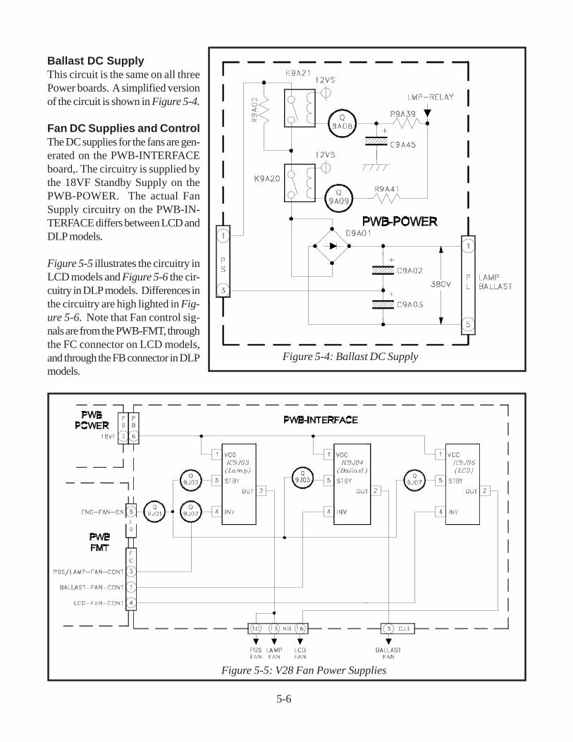
Ballast DC SupplyThis circuit is the same on all threePower boards. A simplified versionof the circuit is shown in Figure 5-4.
Fan DC Supplies and ControlThe DC supplies for the fans are gen-erated on the PWB-INTERFACEboard,. The circuitry is supplied bythe 18VF Standby Supply on thePWB-POWER. The actual FanSupply circuitry on the PWB-IN-TERFACE differs between LCD andDLP models.
Figure 5-5 illustrates the circuitry inLCD models and Figure 5-6 the cir-cuitry in DLP models. Differences inthe circuitry are high lighted in Fig-ure 5-6. Note that Fan control sig-nals are from the PWB-FMT, throughthe FC connector on LCD models,and through the FB connector in DLPmodels.
Figure 5-4: Ballast DC Supply
Figure 5-5: V28 Fan Power Supplies

5-7
PWB-ENG-PWRIt was previously mentioned that the PWB-ENG-PWRboard is added in DLP models. Figure 5-7 shows thiscircuitry. It is basically a PWM Regulator with a pushpull FET output circuit, generating a 2.5V supply for theDLP Engine. The board also serves as an interface forthe 12V, 5V and 3.3V Standby supplies from PWB-POWER.
Hard Disc 7Drive (HDD) SupplyAdditional power supply circuitry is required for theV30+ and V31 chassis. Both of these chassis typesfeature a Hard Disc Drive. Added power circuitry forthe HDD is on the PWB-POWER, refer to Figure 5-8.Note that the Fan Stop monitoring circuit for the HDDis also added to PWB POWER.
Power DistributionWhen a specific PWB is suspected as the cause of aproblem, the following should be checked before or-dering a new board:
• Power supply voltages supplied to the PWB.• Signals supplied to the PWB.
Power Distribution diagrams are helpful in locating thesource of a missing power supply voltage. Figure 5-9shows the Power Distribution for the V28 chassis. Fig-ure 5-10 illustrates Power Distribution in the DLP chas-sis. Although the two chassis types are similar there aresome differences. The shaded areas in Figure 5-10indicate differences from the V28 chassis.
Figure 5-6: V29/V30/V30+/V31 Fan Supplies

5-8
Figure 5-7: DLP Engine Power Supply
Figure 5-8: Hard Disc (HDD) Power Supply(V30+ and V31 Only)

5-9
Figure 5-9

5-10
Figure 5-10

5-11
Video Signal PathAnalog Video PathThe Video signal path is also similar on all the chassistypes. Figure 5-11 illustrates the Basic Analog VideoSignal Path. The Tuners are located on the PWB-DM.The Analog video from the Tuners is directed throughPWB-RISER to the Video Select Circuitry on PWB-MICRO.
The Video Select circuitry is comprised of IC2K01 andIC2KO2. IC2K01 selects the Sub Video signal sourceand the External Video Input source for the Main Pic-ture. It then forwards the External Main Picture signalto IC2K02. IC2K02 selects the main picture sourcefrom the signals from IC2K01, an External Componentinput or the Main Tuner..
The selected Main and Sub Video signals are directedthrough the PWB-RISER to A/D Converters on PWB-DM. The outputs from the A/D Converters are directedto 3DYC, Line Double and PIP/POP circuitry.
The signals from the PWB-DM are directed to thePWB-FORMAT. The signals are digital Y,Pb,Pr. Inthe V28 chassis the signals are in 720p format. In theDLP chassis the signals are in the 1080i format.
On the PWB-FORMAT the signals are processed andconverted to the drive format for that specific Engine. Inthe DLP PWB-FORMAT, the signals are converted from1080i to 1080p.
Figure 5-11:Basic Analog Signal Path

5-12
Digital Video Signal PathFigure 5-12 illustrates the Basic Digital Video SignalPath. The Digital Signal output from the Main Tuner isan I.F. signal. The signal from the Main Tuner is di-rected to PWB-DEMOD1.
The Demodulated Output (MPEG) signals are directback to PWB-DM and via the POD circuitry to theMPEG Decoder. The output of the MPEG Decoder isprocessed by Doubler and PIP/POP circuitry and is di-rected to the PWB-FORMAT.
Note that Prelude and A/D Converter circuitry addedin the DLP chassis PWB-FORMAT. These used forsignal conversion to 1080p and to process signals froma PC. In V29 through V30+ chassis PC connection isthough one of the HDMI inputs on the rear of the TV.
In the V31 chassis a conventional VGA input is addedon the PWB-FORMAT.
Note the in the V30+ and V31 chassis the PWB-DEMOD2 is added to process HD signals from the SubTuner. This allows the Sub Tuner HD signals to be se-lected as the PIP/POP sub picture signal source.
As a reference for troubleshooting, Figures 5-13 through5-15 are more detailed Video Signal Path diagrams:
Figure 5-13: Analog Video Signal PathFigure 5-14: Digital Video Signal PathFigure 5-15: Record Signal Path
Shaded Areas differ from the V28 circuity.
Figure 5-12: Basic Digital Video Signal Path

5-13
Figure 5-13: Analog Video Signal Path

5-14
Figure 5-15: Video Record Path(V30+ and V31 only)
Figure 5-14: Analog Video Signal Path

5-15
Figure 5-16: Sound Signal Path
Sound Signal PathFigure 5-16 shows the Sound Signal Path in both LCDand DLP chassis. The Sound Circuitry is the same onboth LCD and DLP chassis. IC3J01 on PWB-TER-MINAL select the analog sound signal source.The selected signal is directed to PWB-DM.The signal is converted to a digital I2S formatand is applied the Digital Sound Selection por-tion of the HD Processor.
The signal is then directed to an MP3 Switch.If the signal source is digital, it is processed byan MP3 Decoder and is also directed to aninput on the MP3 Switch.
An I2S Decoder converts the selected signalto analog left and right audio. The signals aredirected through PWB-RISER and are pro-cessed by a sound processing IC, then ampli-fied and directed to the set’s speakers.
The only new circuitry is Speaker Short Detect circuitshown in Figure 5-17.
Figure 5-17: Speaker Protect Circuitry

5-16
Control CircuitryOverall Control CircuitryThere are 5 Control µPCs in the LCD and DLP chassis.
• IC7A00 TV µPC on PWB-MICRO• IC8001 DM µPC on PWB-DM• IC7P01 SYS-5 µPC on PWB-MICRO
Figure 5-18: Overall Control Circuitry Block Diagram
• IC8G01 FORMAT µPC on PWB-FORMAT• IC7R05 TVGOS µPC on PWB-RISER
Figure 5-18 shows the interconnect paths between thefive µPCs, and the command input paths from the Re-mote Control and the Front Panel buttons.

5-17
Figure 5-19: V28 Lamp Control Circuitry
Lamp Control CircuitryFigure 5-19 shows the Lamp Control Circuitry in V28chassis, and Figure 5-20 the circuitry in the DLP chas-sis. Differences from the V28 chassis are shaded in
Figure 5-20. Mainly in the V28 the LAMP-EN com-mand is from the FMT µPC, and in the DLP chassis itcomes from the Light Engine
Figure 5-20: DLP Chassis Lamp Control Circuitry
5-18
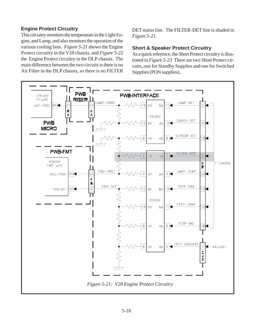
Engine Protect CircuitryThis circuitry monitors the temperature in the Light En-gine, and Lamp, and also monitors the operation of thevarious cooling fans. Figure 5-21 shows the EngineProtect circuitry in the V28 chassis, and Figure 5-22the Engine Protect circuitry in the DLP chassis. Themain difference between the two circuits is there is noAir Filter in the DLP chassis, so there is no FILTER
DET status line. The FILTER-DET line is shaded inFigure 5-21.
Short & Speaker Protect CircuitryAs a quick reference, the Short Protect circuitry is illus-trated in Figure 5-23 There are two Short Protect cir-cuits, one for Standby Supplies and one for SwitchedSupplies (PON supplies)..
Figure 5-21: V28 Engine Protect Circuitry

5-19
Figure 5-22: DLP Engine Protect Circuitry
Figure 5-23: Short Detection Circuitry

5-20


Copyright © 2005 Mitsubishi Digital Electronics America, Inc.9351 Jeronimo Road • Irvine, CA 92618-1904