SEMINAR ON IC FABRICATION MD.ASLAM ADM NO:05-125,ETC/2008.
23
SEMINAR ON IC FABRICATION MD.ASLAM ADM NO:05-125,ETC/2008
-
Upload
candice-andrews -
Category
Documents
-
view
220 -
download
0
Transcript of SEMINAR ON IC FABRICATION MD.ASLAM ADM NO:05-125,ETC/2008.

SEMINAR ON IC FABRICATION
MD.ASLAMADM NO:05-125,ETC/2008

INTRODUCTIONOXIDATIONPHOTOLITHOGRAPHYETCHINGSPUTTERINGDIFFUSIONCHEMICAL DEPOSITIONION IMPLANTIONEPITAXY
HIGHLIGHTS

INTRODUCTION
INTEGRATED CIRCUITS(IC)SARE THE TWENTIETHCENTURY’S MOST IMPORTANTINVENTION.
THE FIRST IC WAS INTRODUCED BY JHON KILBYOF TEXAS INSTRUMENTS

OXIDATION
Oxidation is the processes of converting silicon into silicon dioxide. This process involves directing oxygen against a silicon wafer at a high temperature. The chemical
process is as follows:Method 1) using Oxygen: Si + O2> SiO2Method 2) using Water vapor:Si + H2O SiO2 + 2H2

Above DemonstratesThe wafer oxidation
On the right is the Device containing Several diffusion tubes.

PHOTOLITHOGRAPHY
Photolithography is the process of mask fabrication.This includes the process of transferring a pattern from a mask to the silicon surface.This step is applied many times. The number of masks applied to make the IC is often considered to be a measure of how complex the circuit is.

DEMONSTRATION OF PHOTO-LITHOGRAPHY

ETCHING
Etching is the process of removing layers of unwanted silicon, silicon dioxide, aluminum, and other materials from a wafer. This occurs after a wafer has a layer of photoresist which has been exposed to uv light through a mask.

IMPORTANT THINGS FOR ETCHING
1) Repeatability: being able to reproduce the mask details accurately in the silicon.2) Uniformity: Etch uniformity across the wafer must be consistent.3) Selectivity: Etch Contrast across the wafer must be hightypically 7:1 to 30:1.4) Slope angle control: The slope of the holes created for etching from 0 to 45 degrees must be accurate to allow for later stages of fabrication.5) Operator and Environment Safety: The etching process should have operator safety, plant safety, and environmental safety regulations.

6) Radiation damage: The radiation used in etching must not damage the devices created.
7) Thermal distortion: The heat from etching must not damage the silicon in the wafer.
8) Throughput and capital expense: The wafer throughput must be high enough to satisfy the economic requirements and production demands.
9) Cleanliness: The etching equipment must not contaminate the wafer.
10) Mask removal: The photoresist mask must be completely and easily removed
DEMONSTRATION OF THE ETCHING PROCESS

SPUTTERING
Sputtering and evaporating are non chemical methods of depositing thin films of material, usuallymetals, onto a wafer. Some materials deposited include: aluminum, gold, tungsten, molybdenum,silicon dioxide, and silicon. The process of sputtering and evaporating do not involve a chemical reaction between the silicon and the material being deposited onto it.

MATERIALS ARE THROWN ATTHE SILICON WAFER.

ATOMS BREAK OFF OR SPUTTER

SPUTTERING MACHINE

DIFFUSION
Diffusion is the uniform distribution of impurity atoms (dopants) into a silicon crystal lattice in a wafer. The purpose of introducing impurities is to change the electrical characteristics of silicon to make it either P-type silicon or N-type silicon. Some of the impurities used to produce N-type include: Antimony, Arsenic, and Phosphorus. Some of the impurities used to produce P-type include: Boron, Gallium, and Aluminum.

The P and N sections ,. When joined create an equilibrium. The focus of diffusion is to create these regions on the silicon wafer.
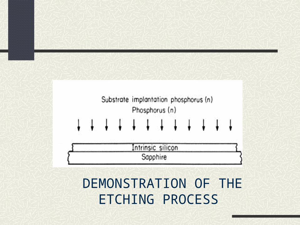
CHEMICAL DEPOSITION
The CVD reactor system shown above is a “hot-wall LPDCVD system using a three-zone furnace”. (Whew say that ten time fast) This would be commonly used to deposit polysilicon, silicon dioxide and silicon nitride. This is referred to as a low pressure CVD (LPCVD) system. The reactant gases are introduced at one end and forced through a three-zone furnace out the other end. (The spike thermo-couples are the 3 zones)

ION IMPLANTATION
Ion implantation is a another procedure to introduce impurity atoms to a silicon wafer. It is like diffusion in its goal but has some advantages. An ion implanter is a high-voltage particle accelerator that produces a beam of impurity atoms which can penetrate the surface of the wafer. The basic parts are described in detail.1. Ion Source. The source operates at a high voltage and produces plasma containing the desired impurity. Solids can be sputtered to give a wide degree of choice in impurities.2. Mass Spectrometer. A big magnet bends the ion beam through a right angle to select the desired impurity. The select ion then passes through a small slit into the main accelerator column. (Consult figure above.)

MAIN COMPONENTS OF AN ION IMPLANTER

3. High-Voltage Accelerator. The accelerator adds up to 175 ke V of energy to accelerate the ions to their final velocity. These are operated at high voltage so they are encased in a protective shield.
4.Scanning System. X and Y deflection plates scan the beam across the wafer to give uniform distribution and dose of impurity to the wafer. 5. Target Chamber. Silicon wafers are the target for impurity ions. For safety the target area is located near a ground and operates in a vacuum.

EPITAXY
The term “epitaxial” means “arranged upon”. An epitaxial film is an essential part of IC fabrication. The process of growing a uniform epitaxial layer on a uniformly doped silicon substrate is known as epitaxy. The use of epitaxy results in a huge (tenfold) increase in yield during the manufacturing process over the old method of applying diffusion three times.