Semiconductor Manufacturing in Japan
21
MAKIMOTO LIBRARY / Exhibit VI / No.1 1 Semiconductor Manufacturing in Japan Dataquest Conference, Phoenix, 1981 Invited Speech Commentary This conference, hosted by Dataquest, was the largest at that time as a semiconductor- related conference, and was held for three days from October 14 to 16 in 1981. In this conference, eminent figures in the leadership position of the semiconductor industry were present including Intel's Robert Noyce, AMD's Jerry Sanders, and Motorola's Gary Tooker. It was the first presentation I made at an international conference; my debut game, so to speak. It still remains in my mind as an unforgettable memory. It can be said that Japan - US semiconductor friction started substantially in this year of 1981. In March of this year, Gene Bylinsky, a magazine-writer wrote a sensational article titled "The Japanese Chip Challenge" in Fortune magazine in the United States. In this period, the 64K bit DRAM generation started to rise and Japanese makers were dominating the market. The basic tone of the article was like this: "If the US loses to Japan in the 64K DRAM competition, the risk is not only limited to the semiconductor industry, but it is also for the computer industry which is much larger than semiconductor." In the autumn of this year, an industry research company reported that Japan acquired 70% of market share with 64 Kbit DRAM, and among them Hitachi took 30% of the world share. In such circumstances, I was the only person invited from Japan to make a speech. It was on the most delicate theme in the situation surrounded by all enemies so to speak. Based on the background of the time, I described the characteristics of semiconductor manufacturing in Japan, quoting examples as familiar as possible. Beginning with the geographical setting in which Japan was placed, I touched on the characteristic features of the Japanese market (consumer field orientation), the technology (strong orientation to lower power, and leading with high speed CMOS) and so on. I then introduced annual events and small group activities which were somewhat special to Japan, and then emphasized the importance of education. An important message I provided in this lecture was that "the future mainstream of semiconductors will shift from NMOS to CMOS". There were many questions from the executives who were familiar with the technology such as, "performance is amazing but how about the manufacturability?“. I think, however, it gave a strong impression as a whole. In conclusion, I sent a cheering message that, "The US is in the top position by far in the semiconductor industry, and particularly strong in the microprocessor field.” I told that Japan was demonstrating the strength in the manufacturing of microfabrication products, in which team works nurtured by small group activities were playing important roles, and emphasized the importance of education to cope with the extremely fast technological advancement in semiconductor industry.
Transcript of Semiconductor Manufacturing in Japan

MAKIMOTO LIBRARY / Exhibit VI / No.1
1
Semiconductor Manufacturing in JapanDataquest Conference, Phoenix, 1981
Invited Speech
Commentary
This conference, hosted by Dataquest, was the largest at that time as a semiconductor-
related conference, and was held for three days from October 14 to 16 in 1981. In this
conference, eminent figures in the leadership position of the semiconductor industry were
present including Intel's Robert Noyce, AMD's Jerry Sanders, and Motorola's Gary
Tooker. It was the first presentation I made at an international conference; my debut
game, so to speak. It still remains in my mind as an unforgettable memory.
It can be said that Japan - US semiconductor friction started substantially in this year of
1981. In March of this year, Gene Bylinsky, a magazine-writer wrote a sensational article
titled "The Japanese Chip Challenge" in Fortune magazine in the United States. In this
period, the 64K bit DRAM generation started to rise and Japanese makers were
dominating the market. The basic tone of the article was like this: "If the US loses to
Japan in the 64K DRAM competition, the risk is not only limited to the semiconductor
industry, but it is also for the computer industry which is much larger than
semiconductor."
In the autumn of this year, an industry research company reported that Japan acquired
70% of market share with 64 Kbit DRAM, and among them Hitachi took 30% of the world
share. In such circumstances, I was the only person invited from Japan to make a
speech. It was on the most delicate theme in the situation surrounded by all enemies so
to speak.
Based on the background of the time, I described the characteristics of semiconductor
manufacturing in Japan, quoting examples as familiar as possible. Beginning with the
geographical setting in which Japan was placed, I touched on the characteristic features
of the Japanese market (consumer field orientation), the technology (strong orientation to
lower power, and leading with high speed CMOS) and so on. I then introduced annual
events and small group activities which were somewhat special to Japan, and then
emphasized the importance of education.
An important message I provided in this lecture was that "the future mainstream of
semiconductors will shift from NMOS to CMOS". There were many questions from the
executives who were familiar with the technology such as, "performance is amazing but
how about the manufacturability?“. I think, however, it gave a strong impression as a
whole.
In conclusion, I sent a cheering message that, "The US is in the top position by far in the
semiconductor industry, and particularly strong in the microprocessor field.” I told that
Japan was demonstrating the strength in the manufacturing of microfabrication products,
in which team works nurtured by small group activities were playing important roles, and
emphasized the importance of education to cope with the extremely fast technological
advancement in semiconductor industry.

MAKIMOTO LIBRARY / Exhibit VI / No.1
2
This speech was given by the invitation from Dataquest. My post at that time was
the Deputy General Manager of Musashi Works of Hitachi, Ltd., to be responsible
for overseeing the all technical departments of MOS products in general.
It was in the midst of the Japan-U.S. semiconductor friction at this time, and I had to
be careful about this point, too.

MAKIMOTO LIBRARY / Exhibit VI / No.1
3
First of all, I touch on the characteristic features of Japan such as geographical setting and natural
disasters. Japan’s land area is about 1/30 of the US, the population about 1/2, and the population
density about 15 times higher. Many natural disasters such as earthquakes, typhoons, volcanic
eruptions etc. have affected the mentality of the Japanese people.
The Japanese semiconductor market grew mainly in consumer applications, however the
proportion of computers and industry sectors is gradually increasing.

MAKIMOTO LIBRARY / Exhibit VI / No.1
4
Technological development and market structure are closely related. In the early 1970s, watches
and calculators were the main drivers in MOS, and TVs and VCRs in bipolar. For watches and
calculators, low cost, low power, and high reliability were required, which led to the development of
highly integrated CMOS, which then spread to memories and microprocessors.
Then I touched on annual events in Japanese business activities; starting from “Hatsumode” in
January (practice of visiting shrines) to year-end parties in December.

MAKIMOTO LIBRARY / Exhibit VI / No.1
5
The Small Group Activity which originally started in the US in the 1950s, and has
settled itself in Japan is explained with some actual examples. This activity is
playing an important role in the Japanese industry. The importance of education can
never be emphasized too much, and some examples are presented.
MAKIMOTO LIBRARY / Exhibit VI / No.1
6
The education of new college graduate employees is introduced with Hitachi’s examples.
As a conclusion, the influence of geographical setting on the differences in mentality between
Japan and the United States was pointed out. Strength of the US was commented; “US is by far
the No. 1 in the semiconductor industry, especially in the field of microprocessors.” Japan's
strength is in the manufacturing of microfabrication products, owing to market background, trends
in technology development, and Small Group Activities, etc.
Figures and explanations follow.

MAKIMOTO LIBRARY / Exhibit VI / No.1
7
The Figure shows locations of semiconductor factories in Japan. Many factories are
concentrated in Kyushu Island, and it is also called "Silicon Island". As one of its
backgrounds, Kyushu has abundance of good water, as is shown by its good
Shochu liquor for which clean water is indispensable. Semiconductor manufacturing
requires abundance of good water, too.

MAKIMOTO LIBRARY / Exhibit VI / No.1
8
It shows the trend of Japanese semiconductor market. In 1975, calculators and
consumer sectors shared large portion, but the proportion of computers,
communications, and industries started to increase in 1980. In the consumer field,
TV market has shrunk, and VCR market has grown.

MAKIMOTO LIBRARY / Exhibit VI / No.1
9
The comparison of the market structure between Japan and the US is shown. As of
1975, the largest market in Japan was the consumer field, and it was the computer
market in the US. In 1980, the proportion of computers has risen in Japan, and the
growth of communication field became prominent in the US.
MAKIMOTO LIBRARY / Exhibit VI / No.1
10
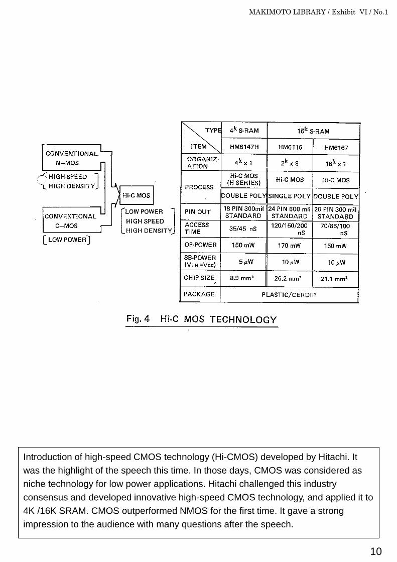
Introduction of high-speed CMOS technology (Hi-CMOS) developed by Hitachi. It
was the highlight of the speech this time. In those days, CMOS was considered as
niche technology for low power applications. Hitachi challenged this industry
consensus and developed innovative high-speed CMOS technology, and applied it to
4K /16K SRAM. CMOS outperformed NMOS for the first time. It gave a strong
impression to the audience with many questions after the speech.

MAKIMOTO LIBRARY / Exhibit VI / No.1
11
The cutting edge technology at the time was with the wafer diameter of 100 mm,
processing level in 3 μ, and the DRAM integration level was 64 Kbits. The prediction
for 1985 was the wafer diameter of 125 mm, the processing level of 2 μ, and the
DRAM integration level of 256 Kbits.

MAKIMOTO LIBRARY / Exhibit VI / No.1
12
This table shows the past and present situations, and the future prospect for MOS
device types; PMOS, NMOS, and CMOS. PMOS ends in the 5 μ era. NMOS leads
its way to 2 μ DRAM (256 K). CMOS was used for watches and calculators in the
past, and it started to be used for SRAM from the 3 μ era, and it will be used for
64Kbit SRAM in 2 μ era. It was a novel and drastic assertion at this time that high
speed devices would also shift from NMOS to CMOS in the future.

MAKIMOTO LIBRARY / Exhibit VI / No.1
13
The rise and fall of MOS devices are shown. Up to 1975, PMOS for calculators
occupied an overwhelming share, but its share gradually decreased, and NMOS
and CMOS grew. In CMOS, the ratio of memory and microprocessor has been
increasing in place of calculators and watches which shared the major portion.

MAKIMOTO LIBRARY / Exhibit VI / No.1
14
National events are shown on the left side, semiconductor-related shows and
conferences in the center, and internal activities are shown on the right side. MMM
was the slogan of Small Group Activities in Hitachi intended to eliminate three bad
M’s; Muri (unreasonable deed), Muda (waste), and Mura (unevenness).

MAKIMOTO LIBRARY / Exhibit VI / No.1
15
A ceremony of "Hatsumode" held on New Year's Day every year. Employees visit a
shrine, purify themselves first and pray to God for safety and prosperity. This is an
extremely Japanese-style event, and it may not have been clearly understood by the
audience. I am afraid that many of them felt rather strange.

MAKIMOTO LIBRARY / Exhibit VI / No.1
16
The Small Circle Activities first started in the United States in the 1950s, and then
spread to Japan in the 1960s, and settled there. It was started in 1972 in Hitachi's
semiconductor operation. Initially it was started as MI (Management Improvement)
movement, then was developed into MMM activities in the next phase intended to
eliminate three bad M’s (Muri, Muda, and Mura).

MAKIMOTO LIBRARY / Exhibit VI / No.1
17
The list A shows the number of company wise annual proposals (in thousands), and
the list B shows the number of annual proposals per employee, both in 1980. In
Hitachi, 4.2 million cases were proposed annually, and 2.61 million cases in
Matsushita (now, Panasonic). Surprised voices were heard among the audience to
the size of such numbers, but we also have similar feeling today (as of 2018).

MAKIMOTO LIBRARY / Exhibit VI / No.1
18
This is to summarize the purpose of Small Circle Activities.

MAKIMOTO LIBRARY / Exhibit VI / No.1
19
Two examples of semiconductor related proposals are shown. These are the cases
which realized actual effects.
A) In order to eliminate the leakage, a glass plate is applied to strengthen the cap.
B) A Teflon rod is used to prevent silver paste from scattering at the last part.

MAKIMOTO LIBRARY / Exhibit VI / No.1
20
Wavy transitions of semiconductor technology are shown here. The figure shows
how intense technological innovation occurs in this field. A new wave rises every five
to ten years, overtaking the previous wave. In other words, technology becomes
obsolete at such a pace in the semiconductor field. Prediction was made that VLSI
would be the biggest segment after 10 years in 1990.
This concept was repeatedly introduced in the later speeches including Keynote at
IEDM in 1982.

MAKIMOTO LIBRARY / Exhibit VI / No.1
21
Educational programs for engineers and managers are introduced, taking the case
of Hitachi semiconductor as the examples. Strong emphasis was made on the
importance of education based on the fact that technology would become obsolete
in 5 to 10 years, as shown in the previous slide (Fig.14).
My concluding remark was that "Human resource is the core of semiconductor
business".