Semiconductor Light Sources and Detectors
21
응용광학 - Optoelectronics Semiconductor Light Sources and Detectors
Transcript of Semiconductor Light Sources and Detectors

응용광학 - Optoelectronics
Semiconductor Light Sources and Detectors

Light Emitting Diodes
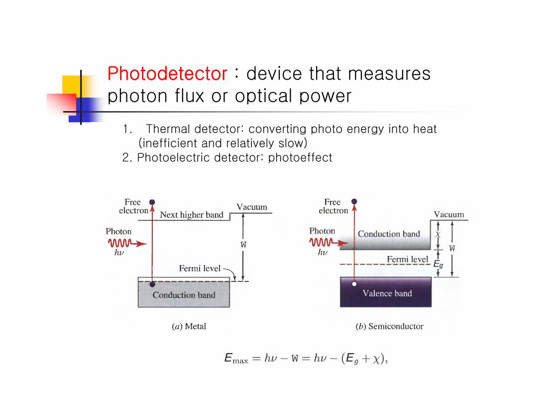
Photodetector : device that measuresphoton flux or optical power
1. Thermal detector: converting photo energy into heat(inefficient and relatively slow)
2. Photoelectric detector: photoeffect
Ec
Ev
Ec
EFp
M
EFn
eVo
p nEo
Evnp
(a)
VI
np
Eo–E
e(Vo–V)
eV
EcEFn
Ev
Ev
Ec
EFp
(b)
(c)
Vr
np
e(Vo+Vr)
EcEFn
Ev
Ev
Ec
EFp
Eo+E (d)
I = Very SmallVr
np
Thermalgeneration Ec
EFnEv
Ec
EFp
Ev
e(Vo+Vr)
Eo+E
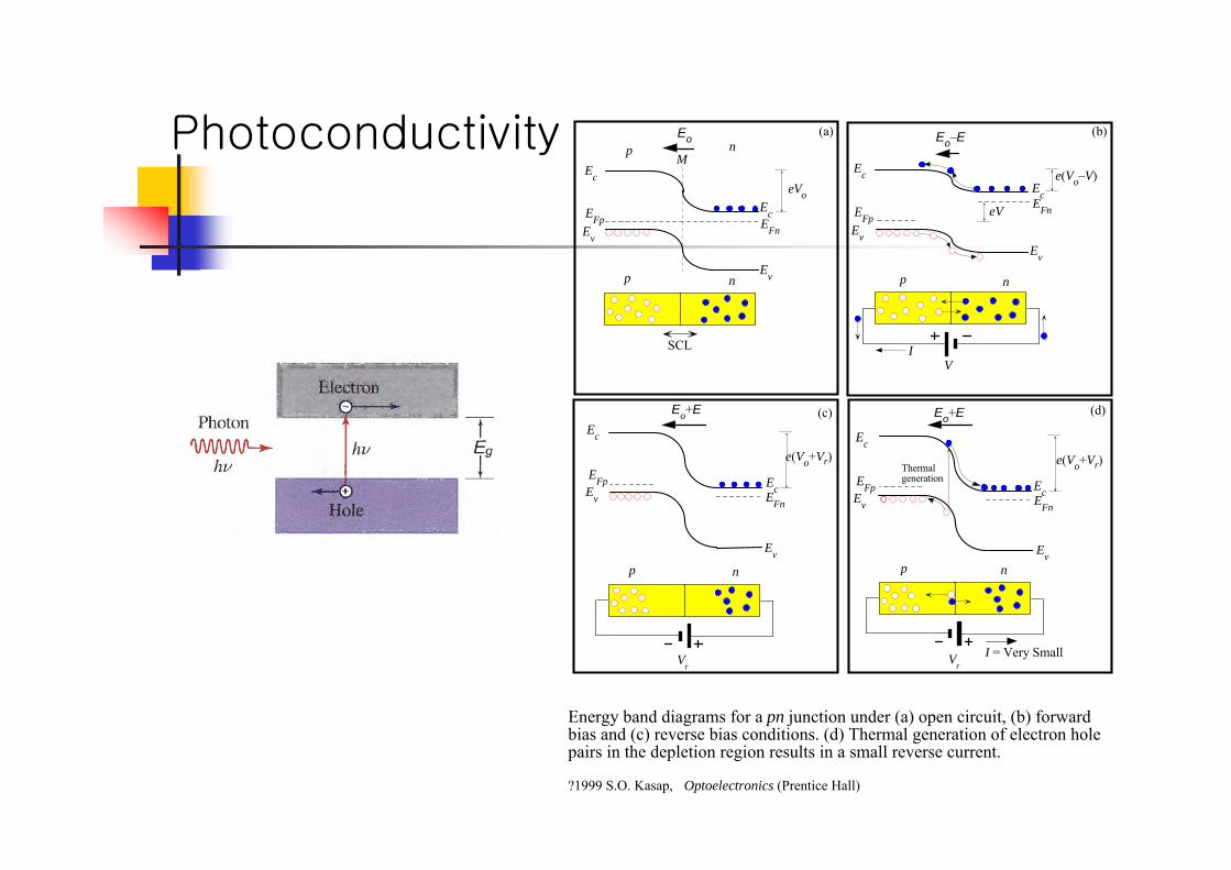
Energy band diagrams for a pn junction under (a) open circuit, (b) forwardbias and (c) reverse bias conditions. (d) Thermal generation of electron holepairs in the depletion region results in a small reverse current.
SCL
?1999 S.O. Kasap, Optoelectronics (Prentice Hall)
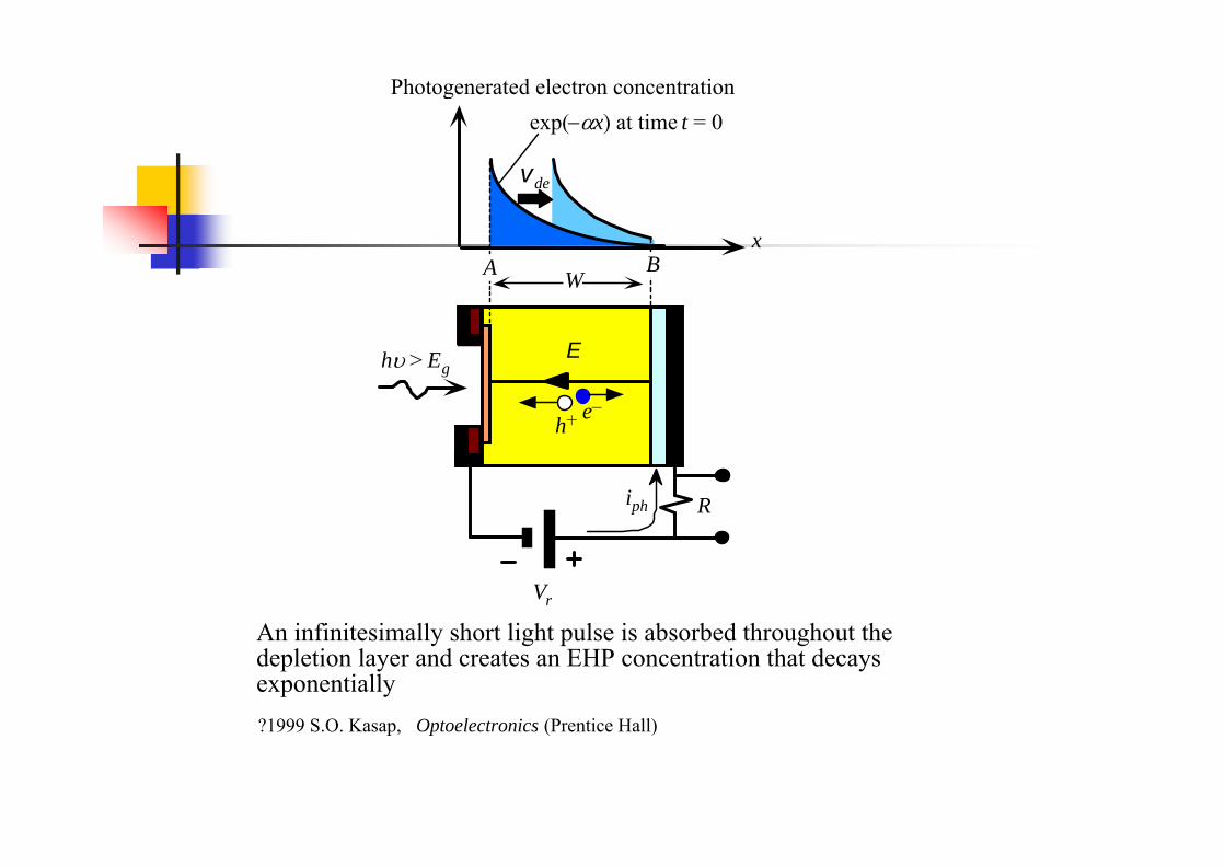
Photoconductivity
x
R
E
e–h+
iph
h> Eg
W
Vr
An infinitesimally short light pulse is absorbed throughout thedepletion layer and creates an EHP concentration that decaysexponentially
Photogenerated electron concentrationexp(x) at time t = 0
BA
vde
?1999 S.O. Kasap, Optoelectronics (Prentice Hall)

xeeIxI )(
0.2 0.4 0.6 0.8 1.2 1.4 1.6 1.8
Wavelength (m)
In0.53Ga0.47As
Ge
Si
In0.7Ga0.3As0.64P0.36
InPGaAs
a-Si:H
12345 0.9 0.8 0.7
1103
1104
1105
1106
1107
1108
Photon energy (eV)
Absorption coefficient () vs. wavelength () for various semiconductors(Data selectively collected and combined from various sources.)
(m-1)
1.0
E
CB
VB
k–k
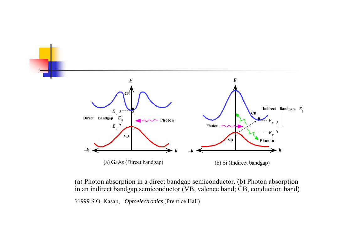
Direct Bandgap Eg Photon
Ec
Ev
(a) GaAs (Direct bandgap)
E
k–k
(b) Si (Indirect bandgap)
VB
CB
Ec
Ev
Indirect Bandgap, Eg
Photon
Phonon
(a) Photon absorption in a direct bandgap semiconductor. (b) Photon absorptionin an indirect bandgap semiconductor (VB, valence band; CB, conduction band)
?1999 S.O. Kasap, Optoelectronics (Prentice Hall)

00.10.20.30.40.50.60.70.8
0.5 1 1.5 2탆Wavelength( )
The responsivity of a commercial Ge pnjunction photodiode
Responsivity(A/W)
?1999 S.O. Kasap, Optoelectronics (Prentice Hall)
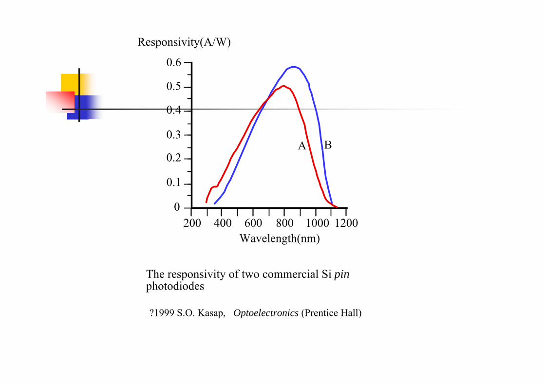
0
0.1
0.2
0.3
0.4
0.5
0.6
200 400 600 800 1000 1200Wavelength(nm)
A B
The responsivity of two commercial Si pinphotodiodes
Responsivity(A/W)
?1999 S.O. Kasap, Optoelectronics (Prentice Hall)
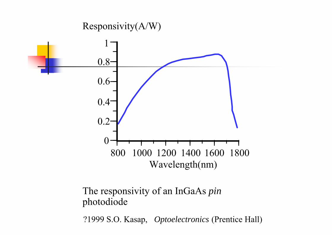
0
0.2
0.4
0.6
0.8
1
800 1000 1200 1400 1600 1800Wavelength(nm)
The responsivity of an InGaAs pinphotodiode
Responsivity(A/W)
?1999 S.O. Kasap, Optoelectronics (Prentice Hall)
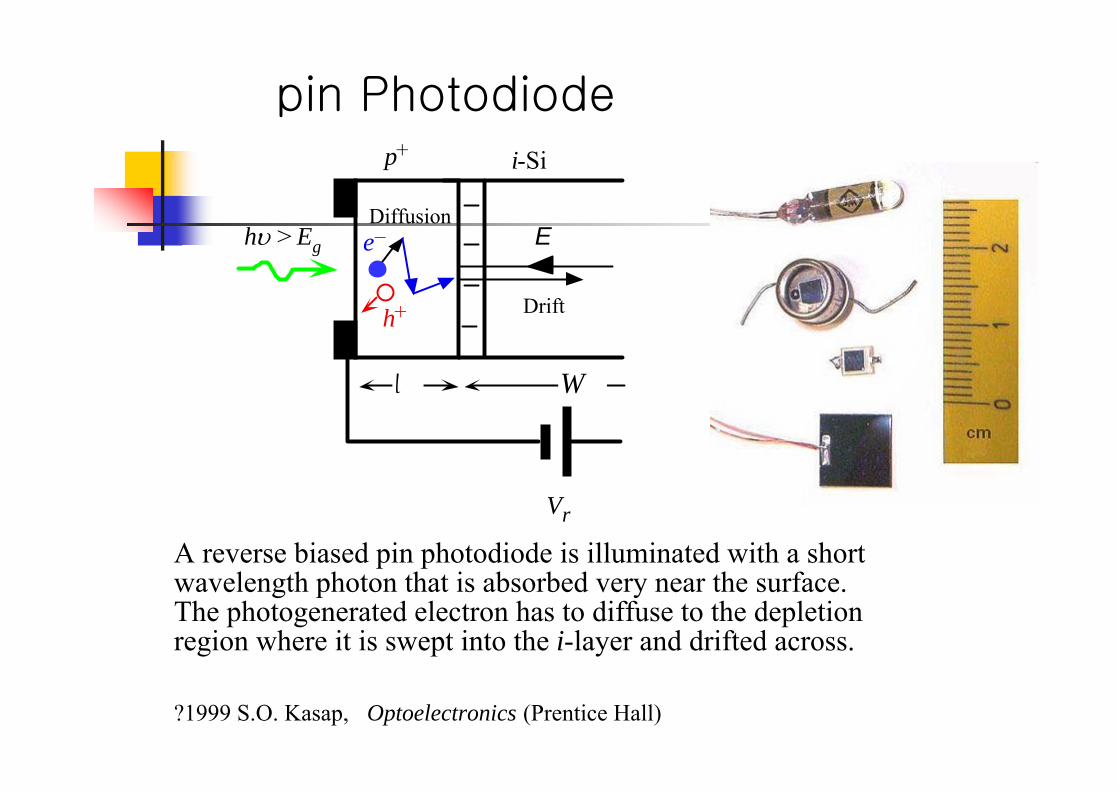
h> Eg
p+ i-Si
e– E
h+
Wl
Drift
Diffusion
A reverse biased pin photodiode is illuminated with a shortwavelength photon that is absorbed very near the surface.The photogenerated electron has to diffuse to the depletionregion where it is swept into the i-layer and drifted across.
Vr
?1999 S.O. Kasap, Optoelectronics (Prentice Hall)
pin Photodiode
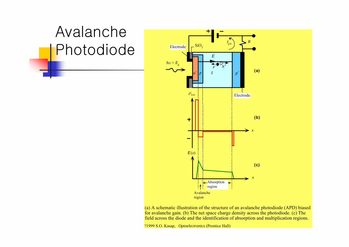
AvalanchePhotodiode
š p+
SiO2Electrode
net
x
x
E(x)
R
Eh > Eg
p
Ip h
e– h+
Absorptionregion
Avalancheregion
(a)
(b)
(c)
(a) A schematic illustration of the structure of an avalanche photodiode (APD) biasedfor avalanche gain. (b) The net space charge density across the photodiode. (c) Thefield across the diode and the identification of absorption and multiplication regions.
Electrode
?1999 S.O. Kasap, Optoelectronics (Prentice Hall)
n+

Vou
Current
Time
Id
Vr
In pn junction and pin devices the main source of noise is shotnoise due to the dark current and photocurrent.
pn
Po
Dark
IlluminatedId + IphId + Ip h + in
R A
?1999 S.O. Kasap, Optoelectronics (Prentice Hall)
Noise of Photodiode
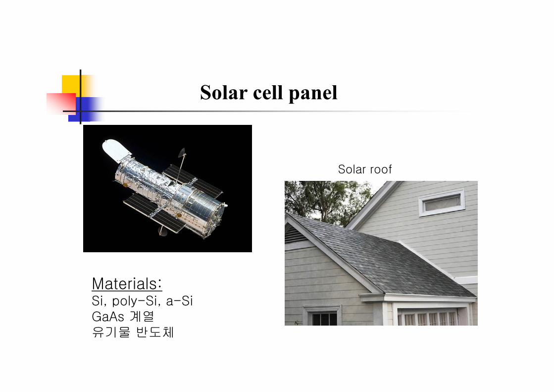
Solar cell panel
Solar roof
Materials:Si, poly-Si, a-SiGaAs 계열유기물 반도체

http://www.nobelprize.org/nobel_prizes/physics/laureates/2009/
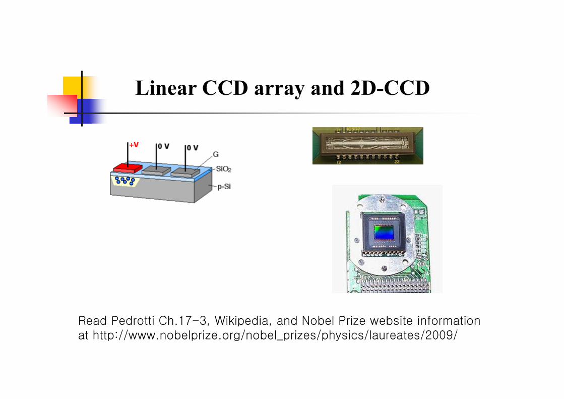
Linear CCD array and 2D-CCD
Read Pedrotti Ch.17-3, Wikipedia, and Nobel Prize website information at http://www.nobelprize.org/nobel_prizes/physics/laureates/2009/
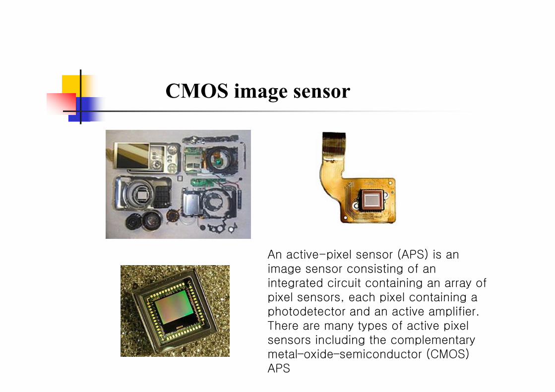
An active-pixel sensor (APS) is an image sensor consisting of an integrated circuit containing an array of pixel sensors, each pixel containing a photodetector and an active amplifier. There are many types of active pixel sensors including the complementary metal–oxide–semiconductor (CMOS) APS
CMOS image sensor