Semiconductor devices
61
Semiconductor Devices Dr G.S. Virdi Director R & D Former Director Grade Scientist GGS College of Modern Technology CSIR- Central Electronic Engineering Kharar Mohali Research Institute- Pilani
-
Upload
gs-virdi -
Category
Technology
-
view
72 -
download
1
Transcript of Semiconductor devices
Semiconductor Devices
Dr G.S. VirdiDirector R & D Former Director Grade Scientist GGS College of Modern Technology CSIR- Central Electronic EngineeringKharar Mohali Research Institute- Pilani
In the modern world no other technology permeates every nook and cranny of our existence as does electronics.
Application of electronics are : Televisions, radios, stereo equipment, computers, scanners, electronic control systems (in cars for example) etc.
Introduction to Electronic Devices

Outline Presentation Introduction Diodes Electrical Properties of Solids Semiconductors P-n Junctions Semiconductor Diodes Diode Circuits
Introduction This course adopts a top-down approach to the
subject and so far we have taken a ‘black-box’ view of active components
It is now time to look ‘inside the box’ we will start by looking at diodes and
semiconductors then progress to transistors later we will look at more detailed aspects of
circuit design

Electronics Components

The p-n junction is at the heart of electronics technology. Most electronics is silicon based, that is, the devices are made of silicon. Silicon wafers are subjected to special procedures which result in what is called p-type silicon material and n-type silicon material. Where these two types of materials meet we have a p-n junction.
p-n junction

Diodes
An ideal diode passing electricity in one direction but not the other

Diodes One application of diodes is in rectification
the example below shows a half-wave rectifier
Inpractice, no real diode has ideal characteristics but semiconductor p-n junctions make good diodes
To understand such devices we need to look at some properties of materials

Atomic Structure of atom,
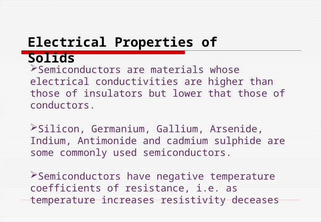
Semiconductors are materials whose electrical conductivities are higher than those of insulators but lower that those of conductors. Silicon, Germanium, Gallium, Arsenide, Indium, Antimonide and cadmium sulphide are some commonly used semiconductors.
Semiconductors have negative temperature coefficients of resistance, i.e. as temperature increases resistivity deceases
Electrical Properties of Solids

Energy Band Diagram Conduction band Ec
Ev
Eg
Band gap
Valence band
Energy band diagram shows the bottom edge of conduction band, Ec , and top edge of valence band, Ev .
Ec and Ev are separated by the band gap energy, Eg .

Energy Bands in Insulators and Conductors
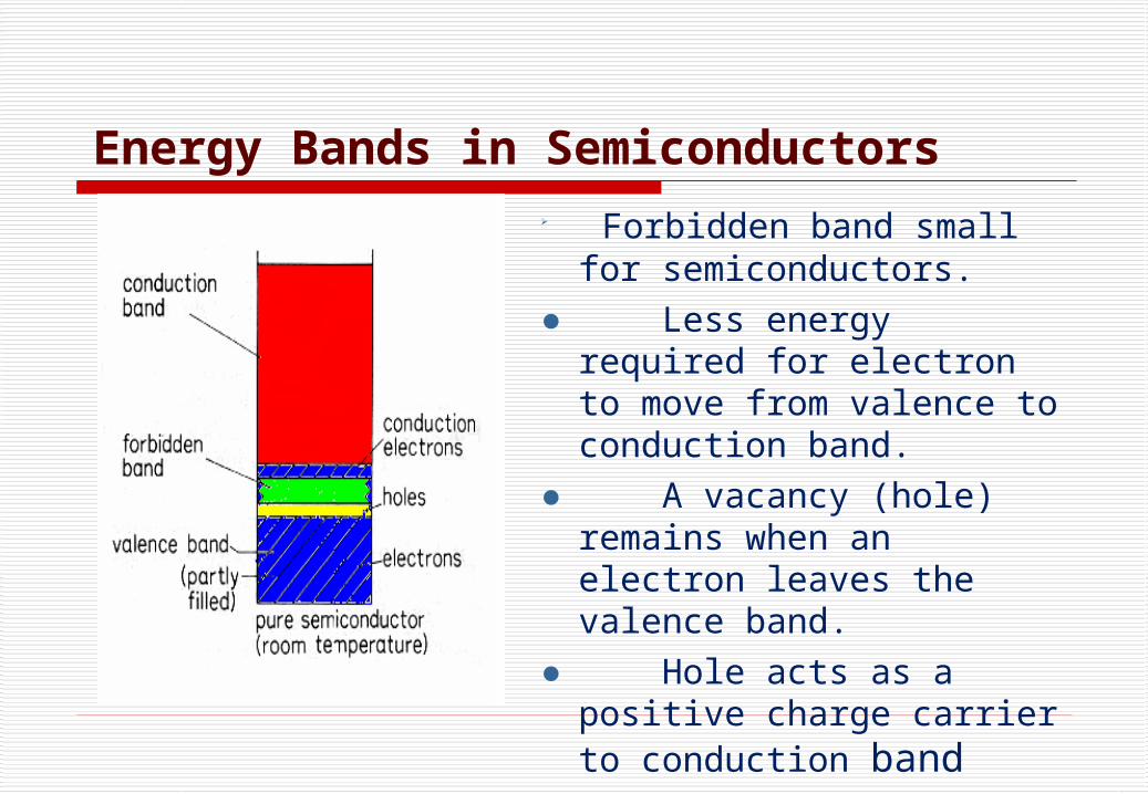
Energy Bands in Semiconductors Forbidden band small for
semiconductors.● Less energy required
for electron to move from valence to conduction band.
● A vacancy (hole) remains when an electron leaves the valence band.
● Hole acts as a positive charge carrier to conduction band

Energy gap in a conductor, semi conductor, and insulator?.Conductor - no energy gapSemi Conductor - 1. 1 ev.Insulator 6 -9 ev.
Energy Bands in Insulators & Semiconductors and Metals

Electrical Properties of Solids Conductors
e.g. copper or aluminium have a cloud of free electrons (at all temperatures
above absolute zero). If an electric field is applied electrons will flow causing an electric current
Insulators e.g. polythene electrons are tightly bound to atoms so few can
break free to conduct electricity

Electrical Properties of Solids
Semiconductors e.g. silicon or germanium at very low temperatures these have the properties of
insulators as the material warms up some electrons break free
and can move about, and it takes on the properties of a conductor - albeit a poor one
however, semiconductors have several properties that make them distinct from conductors and insulators

Silicon Crystal Structure
Unit cell of silicon crystal is cubic.
Each Si atom has 4 nearest neighbors.
Electrical Properties of Solids

Electrical Properties of Solids Pure semiconductors
thermal vibration results in some bonds being broken generating free electrons which move about
these leave behind holes which accept electrons from adjacent atoms and therefore also move about
electrons are negative charge carriers holes are positive charge carriers At room temperatures there are few charge carriers pure semiconductors are poor conductors this is intrinsic conduction

Electrical Properties of Solids
Doping the addition of small amounts of impurities
drastically affects its properties some materials form an excess of electrons
and produce an n-type semiconductor some materials form an excess of holes and
produce a p-type semiconductor both n-type and p-type materials have much
greater conductivity than pure semiconductors this is extrinsic conduction
Extrinsic Semiconductors / Doping
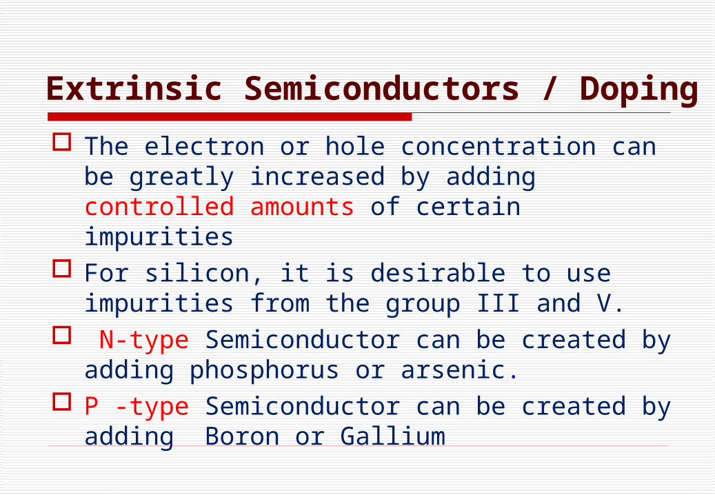
The electron or hole concentration can be greatly increased by adding controlled amounts of certain impurities
For silicon, it is desirable to use impurities from the group III and V.
N-type Semiconductor can be created by adding phosphorus or arsenic.
P -type Semiconductor can be created by adding Boron or Gallium
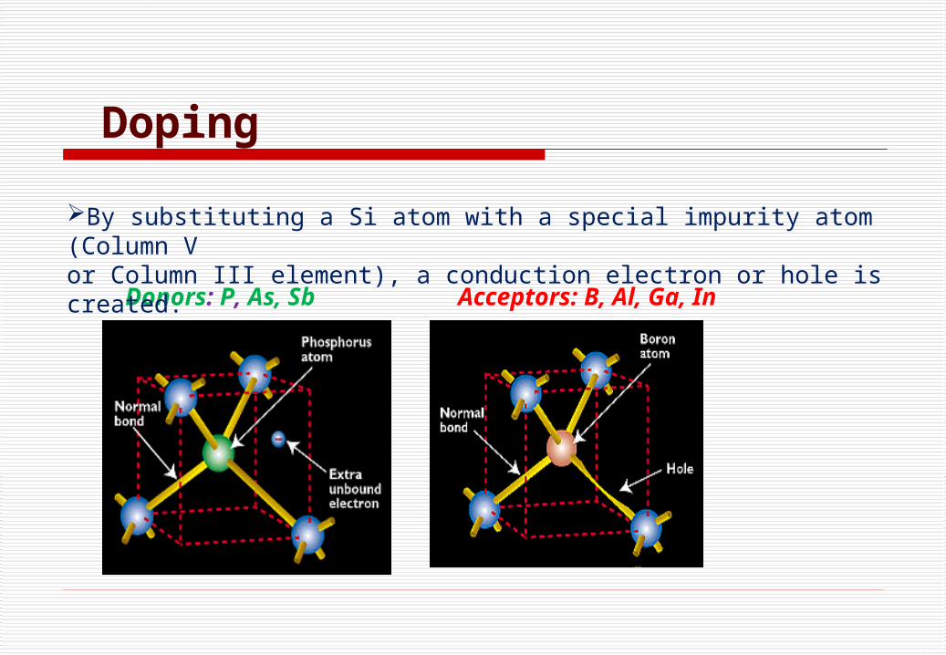
Donors: P, As, Sb Acceptors: B, Al, Ga, In
By substituting a Si atom with a special impurity atom (Column Vor Column III element), a conduction electron or hole is created.
Doping

Electrical Properties of Solids
The dominant charge carriers in a doped semiconductor (e.g. electrons in n-type material) are called majority charge carriers. Other type are minority charge carriers
The overall doped material is electrically neutral
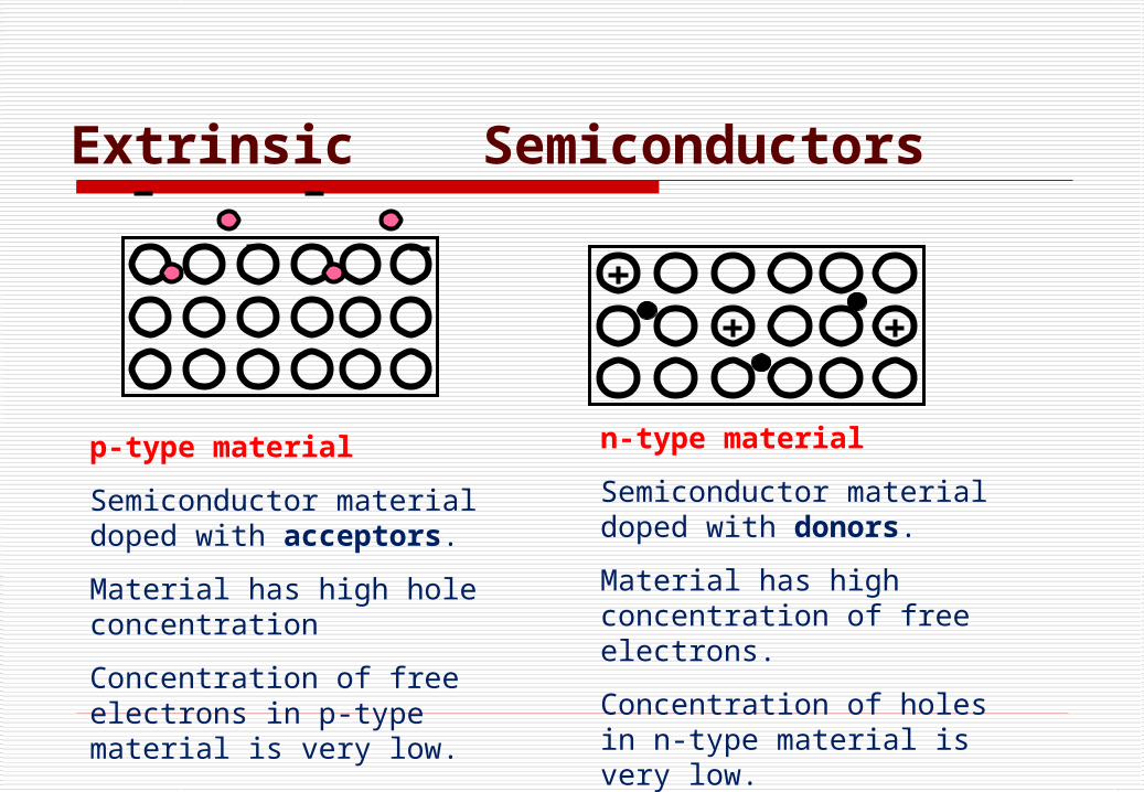
p-type material
Semiconductor material doped with acceptors.
Material has high hole concentration
Concentration of free electrons in p-type material is very low.
n-type material
Semiconductor material doped with donors.
Material has high concentration of free electrons.
Concentration of holes in n-type material is very low.
Extrinsic Semiconductors

p-type material
Contains NEGATIVELY charged acceptors (immovable) and POSITIVELY charged holes (free).
Total charge = 0
n-type material
Contains POSITIVELY charged donors (immovable) and NEGATIVELY charged free electrons.
Total charge = 0
Extrinsic Semiconductors
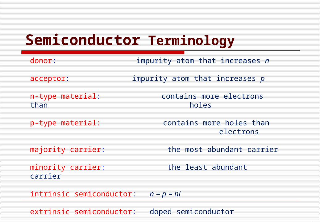
donor: impurity atom that increases n
acceptor: impurity atom that increases p
n-type material: contains more electrons than holes
p-type material: contains more holes than
electrons
majority carrier: the most abundant carrier
minority carrier: the least abundant carrier
intrinsic semiconductor: n = p = ni
extrinsic semiconductor: doped semiconductor
Semiconductor Terminology
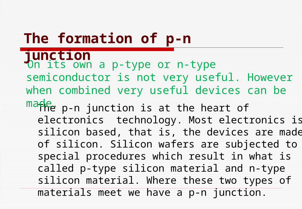
The p-n junction is at the heart of electronics technology. Most electronics is silicon based, that is, the devices are made of silicon. Silicon wafers are subjected to special procedures which result in what is called p-type silicon material and n-type silicon material. Where these two types of materials meet we have a p-n junction.
On its own a p-type or n-type semiconductor is not very useful. However when combined very useful devices can be made.
The formation of p-n junction

The p-n junction is the basic element of all bipolar devices. Its main electrical property is that it rectifies (allow current to flow easily in one direction only).The p-n junction is often just called a DIODE. Applications;
>photodiode, light sensitive diode,>LED- ligth emitting diode,>varactor diode-variable capacitance diode
transistors and integrated circuits
The formation of p-n junction
The p-n junction can be formed by pushing a piece of p-type silicon into close contact with a piecce of n-type silicon. But forming a p-n junction is not so simply. Because;
There will only be very few points of contact and any current flow would be restricted to these few points instead of the whole surface area of the junction.
Silicon that has been exposed to the air always has a thin oxide coating on its surface called the “native oxide”. This oxide is a very good insulator and will prevent current flow.
Bonding arrangement is interrupted at the surface; dangling bonds.
The formation of p-n junction

A P-N Junction cannot be produced by simply pushing two pieces together or by welding etc…..Because it gives rise to discontinuities across the crystal structure.
Special fabrication techniques are adopted to form P-N Junction, e.g. Crystal Preparation , Masking, Photolithographic Process , Deposition ,Implantation , Diffusion ,Oxidation ,Epitaxy ,Contacts, Interconnects ,Metallization and Planarization.
The formation of p-n junction

To overcome these surface states problems
p-n junction can be formed in the bulk of the semiconductor, away from the
surface as much as possible.
Surface states
The formation of p-n junction

The formation of p-n junction
PN junction is present in perhaps every semiconductor device.
diodesymbol
N P
VI
– + Building Blocks of the PN Junction Theory
V
I
Reverse bias Forward bias
Donor ions
N-type
P-type

The formation of p-n junction
When p-type and n-type materials are joined this forms a pn junction majority charge carriers on each side diffuse
across the junction where they combine with (and remove) charge carriers of the opposite polarity
hence around the junction there are few free charge carriers and we have a depletion layer (also called a space-charge layer)
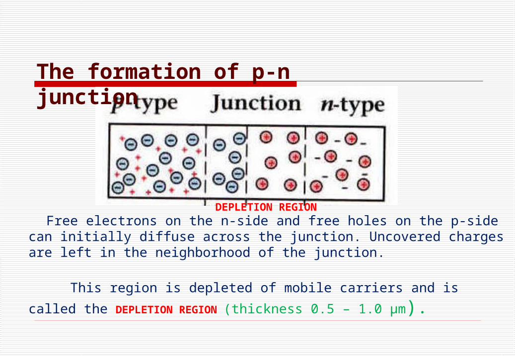
DEPLETION REGION Free electrons on the n-side and free holes on the p-side can initially
diffuse across the junction. Uncovered charges are left in the neighborhood of the junction.
This region is depleted of mobile carriers and is called the
DEPLETION REGION (thickness 0.5 – 1.0 µm).
The formation of p-n junction

The formation of p-n junction
The diffusion of positive charge in one direction and negative charge in the other produces a charge imbalance this results in a
potential barrier across the junction

++++++++++++++++++++++++++++++++++++++++
- - - - - - - - - - - - - - - - - - - - - - - - - - - - - - - - - - - - - - - -
Hole Movement
ElectronMovement
++++++++++++
Fixed positive space-charge
- - - -- - - -- - - -
Fixed negativespace-charge
Ohmic end-contact
n-type p-type
Metallurgical junction
The formation of p-n junction

The formation of p-n junction
Potential barrier the barrier opposes the flow of majority charge
carriers and only a small number have enough energy to surmount it this generates a small diffusion current
the barrier encourages the flow of minority carriers and any that come close to it will be swept over this generates a small drift current
for an isolated junction these two currents must balance each other and the net current is zero

Forward bias to p-n junction
When an external voltage is applied to the P-N junction making the P side positive with respect to the N side the diode is said to be forward biased (F.B). The barrier p.d. is decreased by the external applied voltage. The depletion
band narrows which urges majority carriers to flow across the junction.
A F.B. diode has a very low resistance.

Forward bias to p-n junction
Forward bias if the p-type side is made positive with respect to
the n-type side the height of the barrier is reduced
more majority charge carriers have sufficient energy to surmount it
the diffusion current therefore increases while the drift current remains the same
there is thus a net current flow across the junction which increases with the applied voltage

When an external voltage is applied to the PN junction making the P side negative with respect to the N side the diode is said to be Reverse Biased (R.B.).
The barrier p.d. increases. The depletion band widens preventing the movement of majority carriers across the junction.
A R.B. diode has a very high resistance.
Reversed bias to p-n junction

Reversed bias to p-n junction
Reverse bias if the p-type side is made negative with respect to the
n-type side the height of the barrier is increased the number of majority charge carriers that have
sufficient energy to surmount it rapidly decreases the diffusion current therefore vanishes while the drift
current remains the same thus the only current is a small leakage current caused
by the (approximately constant) drift current the leakage current is usually negligible (a few nA)

Currents in a pn junction
Currents in a pn junction

Forward and reverse currents
Forward and reverse currents pn junction current is given approximately by
where I is the current, e is the electronic charge, V is the applied voltage, k is Boltzmann’s constant, T is the absolute temperature and (Greek letter eta) is a constant in the range 1 to 2 determined by the junction material
for most purposes we can assume = 1
1exp
ηkTeV
II s

Semiconductor Diodes
Thus
at room temperature e/kT ~ 40 V-1
If V > +0.1 V
If V < -0.1 V
IS is the reverse saturation current
1exp
kTeV
II s
VIkTeV
II ss 40expexp
ss III 10

Semiconductor Diodes
Forward and reverse currents
19.6

Silicon diodes
Silicon diodes generally have a turn-on voltage of about 0.5 V generally have a conduction voltage of about 0.7 V have a breakdown voltage that depends on their
construction perhaps 75 V for a small-signal diode perhaps 400 V for a power device
have a maximum current that depends on their construction perhaps 100 mA for a small-signal diode perhaps many amps for a power device

I-V characteristics of electronic components.
Resistor
The I-V plot represents is the dependence of the current I through the component on the voltage V across it.
VR
IRIV
1;I = V /
R;R = V/I
V
I
R
VI
tg() = 1/R
The I-V characteristic of the resistor

Silicon diodesTurn-on and breakdown voltages for a silicon
device

There is no turn-on voltage because current flows in any case. However , the turn-on voltage can be defined as the forward bias required to produce a given amount of forward current.
If 1 m A is required for the circuit to work, 0.7 volt can be called as turn-on voltage.
VVbb
II00VVbb ; Breakdown voltage
II0 ;0 ; Reverse saturation current
Forward BiasForward BiasReverse BiasReverse Bias
I(current)
V(voltage)
Ge ~ 0.2 – 0.4 V
Si ~ 0.6 – 0.8 V
Applying bias to p-n junction

The experimental I-V characteristic of a Si diode
Small leakagecurrent

Temperature dependence of the volt ampere of a p-n diode

Diode Circuits
Half-wave rectifier peak output voltage
is equal to the peak input voltage minus the conduction voltage of the diode
reservoir capacitor used to produce a steadier output

Diode Circuits
Full-wave rectifier use of a diode
bridge reducesthe time for whichthe capacitor hasto maintain theoutput voltageand thus reducedthe ripple voltage

Diode Circuits Signal rectifier
used to demodulatefull amplitudemodulated signals(full-AM)
also known as anenvelope detector
found in a wide rangeof radio receivers fromcrystal sets to super heterodynes

Diode Circuits
Signal clamping a simple form of
signal conditioning
circuits limit theexcursion of thevoltage waveform
can use a combination of signal and Zenerdiodes

Key Points of Diode
Diodes allow current to flow in only one direction At low temperatures semiconductors act like insulators At higher temperatures they begin to conduct Doping of semiconductors leads to the production of p-
type and n-type materials A junction between p-type and n-type semiconductors
has the properties of a diode Silicon semiconductor diodes approximate the behavior
of ideal diodes but have a conduction voltage of about 0.7 V
There are also a wide range of special purpose diodes Diodes are used in a range of applications

Parameter Germanium Silicon Comments
Depletion layer p.d. 0.15V 0.6VGermanium can be useful for low voltage applications.
Forward currentA few milli-Amperes
Tens of Amperes
Silicon much better for high current applications.
Reverse leakage current A few micro-amperes
A few nano-amperes
Germanium 1000 times more leaky than silicon.
Max. reverse voltage VoltsHundreds of volts
Silicon the only real choice for high voltage applications.
Temperature stability Poor GoodGermanium more sensitive to temperature. Can be a problem or can be useful.
Junction capacitanceVery low (point contact)
Comparatively high
This is a useful feature for high frequency use. Note: low capacitance silicon diodes are also available but their capacitance is still higher than point contact type.
Silicon & Germanium diode Comparison

Semiconductor Devices
G.S.VIRDI
• Crystal Preparation
• Masking
• Photolithographic Process
• Deposition
• Implantation
• Diffusion
• Oxidation
• Epitaxy
• Contacts, Interconnect ,Metalization and Planarizatiomn
IC Fabrication Techniques

IC Fabrication LaboratoryG.S.VIRDI
Semiconductor Devices

Design of an Integrated Circuit
Thorough Inspection of Design
Fully Processed WaferSTAGES OF IC FABRICATION
G.S.VIRDI
Semiconductor Devices

60Micro-Fabrication Facilities, CEERI
Fabricated 4” Silicon Wafer – MEMS Acoustic Sensor
MEMS Devices
Semiconductor Devices
G.S.VIRDI

G.S.VIRDI
Semiconductor Devices

![Semiconductor Devices [Kanaan Kano]](https://static.fdocuments.in/doc/165x107/55cf931a550346f57b9bb747/semiconductor-devices-kanaan-kano.jpg)