Segmented-Channel Si 1-xGe /Si pMOSFET for Improved ION ...tking/presentations/Ho_2012VLSI... ·...
23
Symposia on VLSI Technology and Circuits Segmented-Channel Si 1-x Ge x /Si pMOSFET for Improved I ON and Reduced Variability Byron Ho 1 , Nuo Xu 1 , Bingxi Wood 2 , Vinh Tran 2 , Saurabh Chopra 2 , Yihwan Kim 2 , Bich-Yen Nguyen 3 , Olivier Bonnin 3 , Carlos Mazure 3 , Satheesh Kuppurao 2 , Chorng-Ping Chang 2 , Tsu-Jae King Liu 1 1 University of California at Berkeley, 2 Applied Materials, Inc. 3 Soitec
-
Upload
phamnguyet -
Category
Documents
-
view
214 -
download
0
Transcript of Segmented-Channel Si 1-xGe /Si pMOSFET for Improved ION ...tking/presentations/Ho_2012VLSI... ·...
Symposia on VLSI Technology and Circuits
Segmented-Channel Si1-xGex/Si pMOSFETfor Improved ION and Reduced Variability
Byron Ho1, Nuo Xu1, Bingxi Wood2, Vinh Tran2, Saurabh Chopra2, Yihwan Kim2, Bich-Yen Nguyen3,
Olivier Bonnin3, Carlos Mazure3, SatheeshKuppurao2, Chorng-Ping Chang2, Tsu-Jae King Liu1
1University of California at Berkeley, 2Applied Materials, Inc. 3Soitec
Outline• Introduction
– Why silicon-germanium (Si1-xGex) ?– Segmented-channel MOSFET (SegFET) design
• Device Fabrication– Corrugated substrate– p-channel MOSFETs
• Results and Discussion• Conclusion
Slide 1
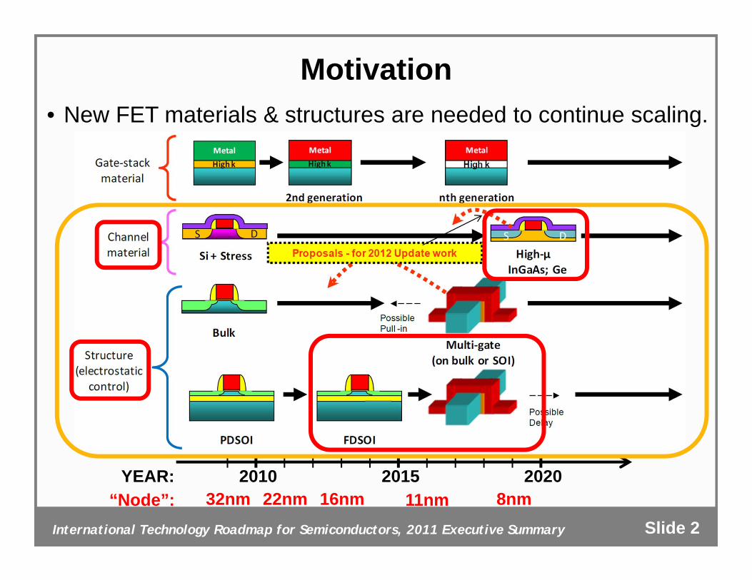
Motivation• New FET materials & structures are needed to continue scaling.
Slide 2International Technology Roadmap for Semiconductors, 2011 Executive Summary
2010 2015 2020YEAR:“Node”: 16nm32nm 22nm 11nm 8nm
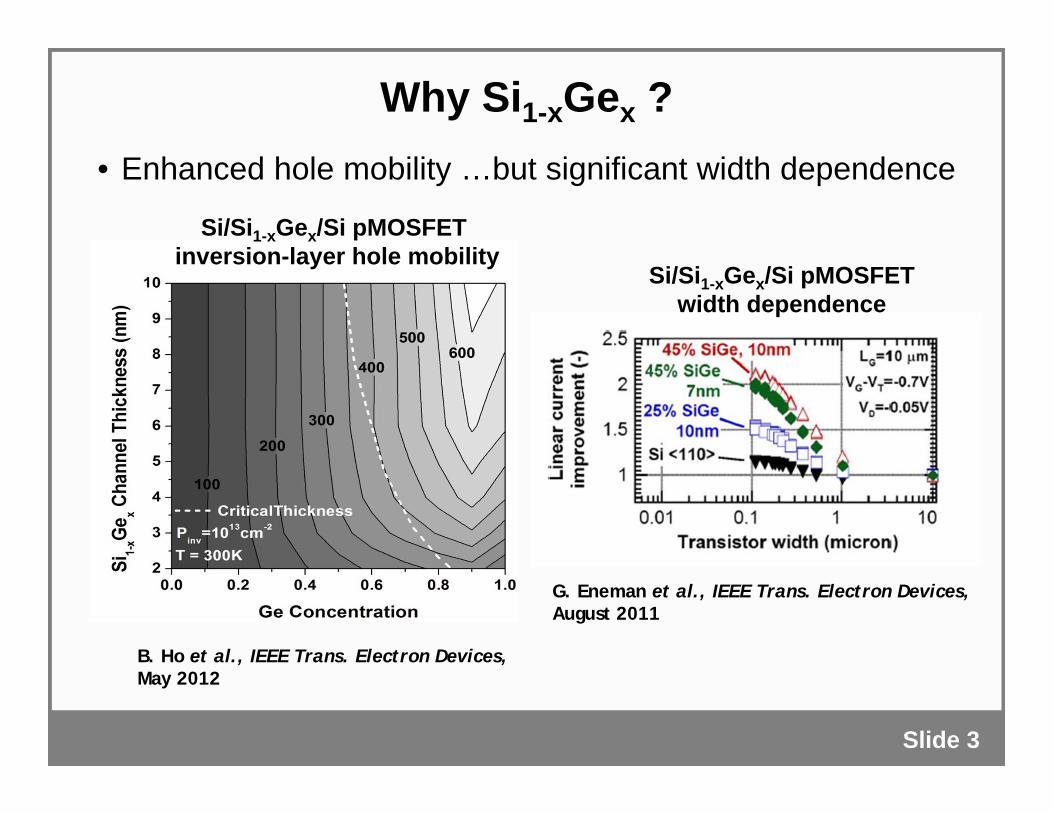
Why Si1-xGex ?
Slide 3
• Enhanced hole mobility …but significant width dependence
Si/Si1-xGex/Si pMOSFETinversion-layer hole mobility
B. Ho et al., IEEE Trans. Electron Devices,May 2012
G. Eneman et al., IEEE Trans. Electron Devices, August 2011
Si/Si1-xGex/Si pMOSFETwidth dependence
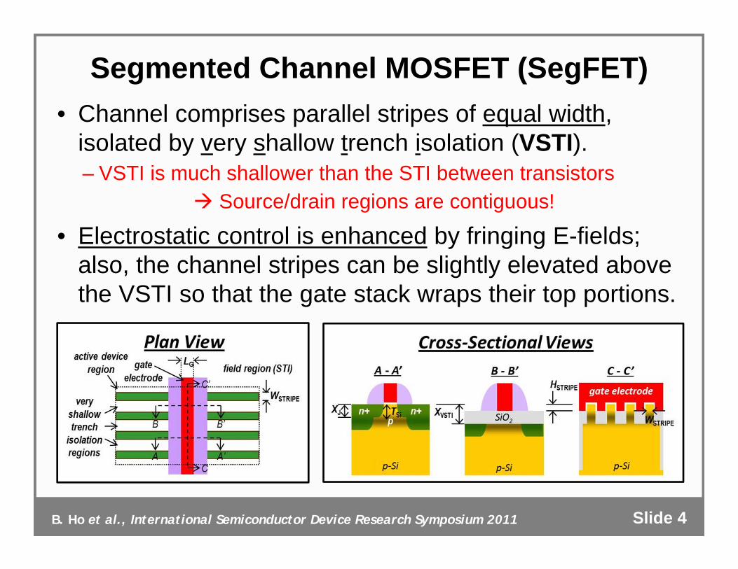
Segmented Channel MOSFET (SegFET)• Channel comprises parallel stripes of equal width,
isolated by very shallow trench isolation (VSTI).– VSTI is much shallower than the STI between transistors
Source/drain regions are contiguous!
• Electrostatic control is enhanced by fringing E-fields; also, the channel stripes can be slightly elevated above the VSTI so that the gate stack wraps their top portions.
Slide 4B. Ho et al., International Semiconductor Device Research Symposium 2011
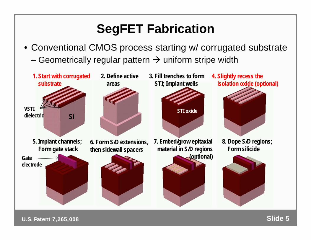
SegFET Fabrication• Conventional CMOS process starting w/ corrugated substrate
– Geometrically regular pattern uniform stripe width
Slide 5U.S. Patent 7,265,008
Gate electrode
STI oxideSi
VSTIdielectric
1. Start with corrugated substrate
2. Define active areas
3. Fill trenches to formSTI; Implant wells
4. Slightly recess theisolation oxide (optional)
5. Implant channels;Form gate stack
7. Embed/grow epitaxial material in S/D regions
(optional)
8. Dope S/D regions;Form silicide
6. Form S/D extensions, then sidewall spacers
This Work
• Fabrication of segmented vs. conventional (non-segmented) Si1-xGex/Si pMOSFETs using the same process flowi.e., corrugated substrate vs. non-corrugated substrate
• Comparison of MOSFET drive current per unit layout widthi.e., layout area efficiency
• Comparison of active area width dependence
Slide 6
Outline• Introduction
– Why silicon-germanium (Si1-xGex) ?– Segmented-channel MOSFET (SegFET) design
• Device Fabrication– Corrugated substrate– p-channel MOSFETs
• Results and Discussion• Conclusion
Slide 7
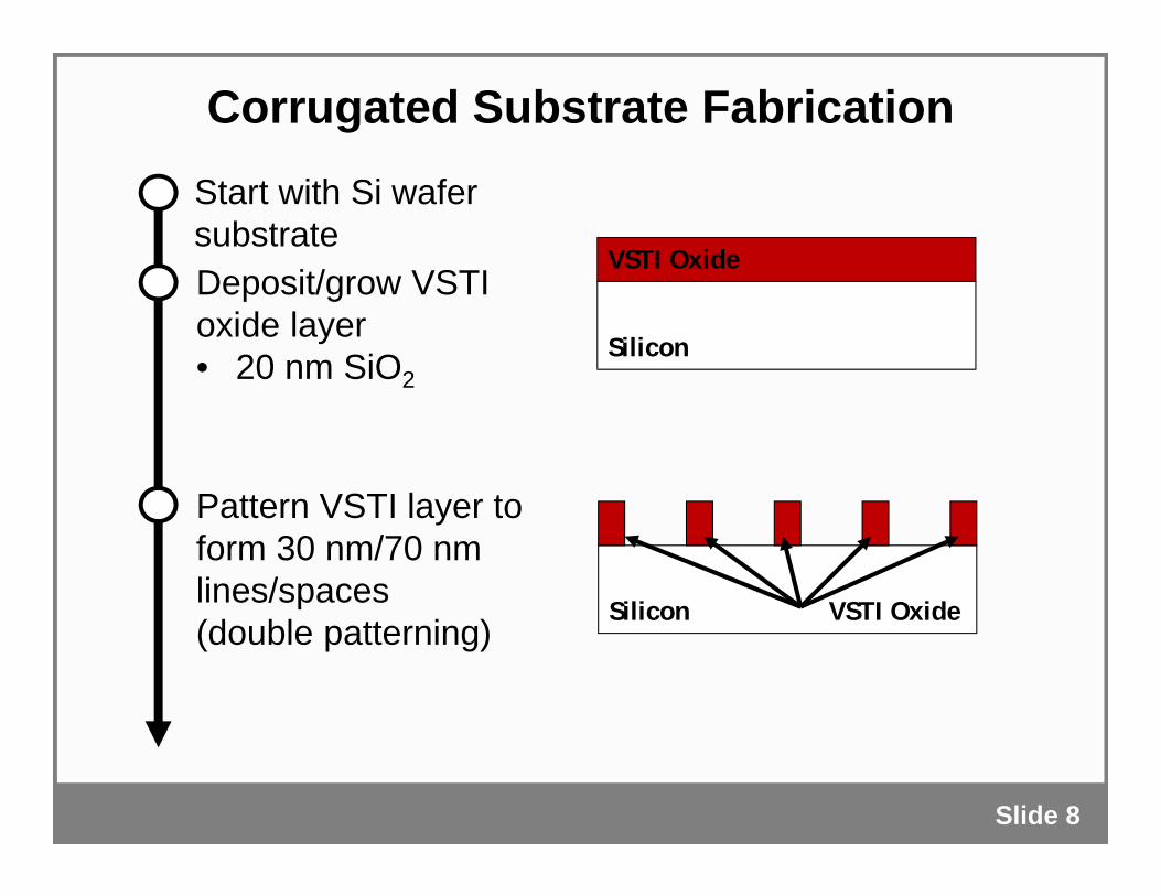
Corrugated Substrate Fabrication
Slide 8
VSTI Oxide
Silicon
Silicon VSTI Oxide
Start with Si wafersubstrateDeposit/grow VSTI oxide layer• 20 nm SiO2
Pattern VSTI layer to form 30 nm/70 nm lines/spaces(double patterning)
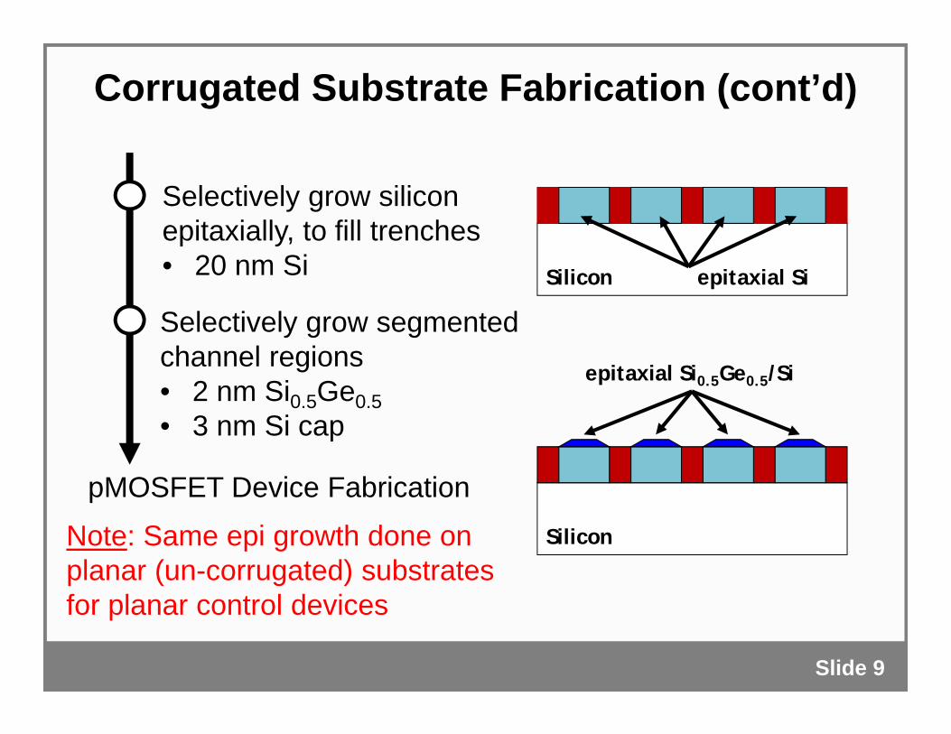
Corrugated Substrate Fabrication (cont’d)
Slide 9
Silicon epitaxial Si
Silicon
epitaxial Si0.5Ge0.5/Si
Selectively grow silicon epitaxially, to fill trenches• 20 nm Si
Selectively grow segmented channel regions • 2 nm Si0.5Ge0.5• 3 nm Si cap
pMOSFET Device Fabrication
Note: Same epi growth done on planar (un-corrugated) substrates for planar control devices
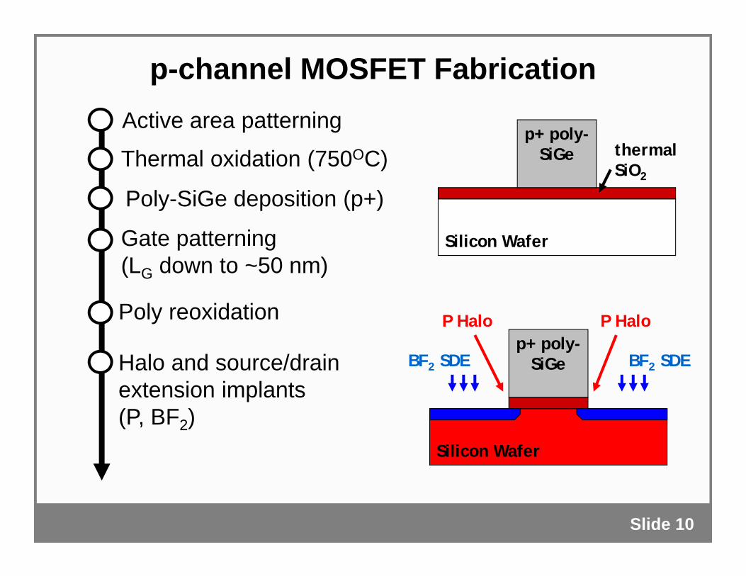
p-channel MOSFET Fabrication
Slide 10
thermal SiO2
Silicon Wafer
p+ poly-SiGe
Silicon Wafer
p+ poly-SiGe
P Halo P Halo
BF2 SDEBF2 SDE
Active area patterning
Thermal oxidation (750OC)
Poly-SiGe deposition (p+)
Gate patterning(LG down to ~50 nm)
Poly reoxidation
Halo and source/drain extension implants(P, BF2)
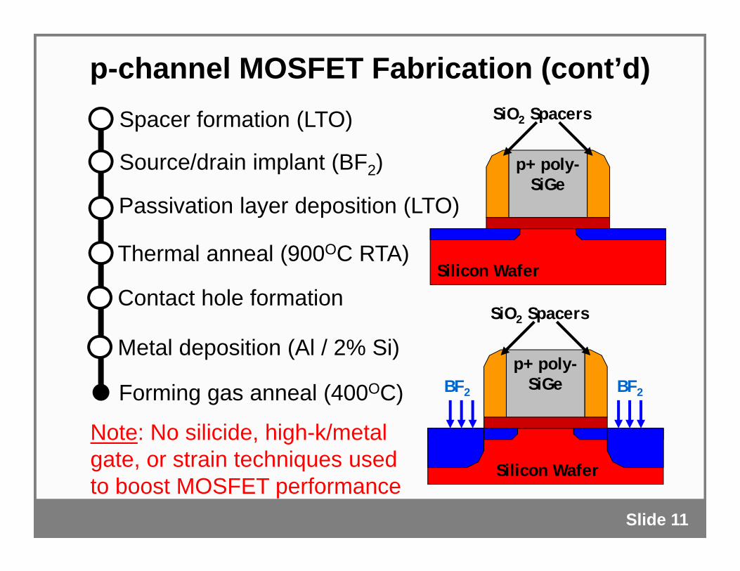
p-channel MOSFET Fabrication (cont’d)
Slide 11
Silicon Wafer
p+ poly-SiGe
SiO2 Spacers
Silicon Wafer
p+ poly-SiGe
SiO2 Spacers
BF2 BF2
Spacer formation (LTO)
Source/drain implant (BF2)
Passivation layer deposition (LTO)
Thermal anneal (900OC RTA)
Contact hole formation
Metal deposition (Al / 2% Si)
Forming gas anneal (400OC)
Note: No silicide, high-k/metal gate, or strain techniques used to boost MOSFET performance

Outline• Introduction
– Why silicon-germanium (Si1-xGex) ?– Segmented-channel MOSFET (SegFET) design
• Device Fabrication– Corrugated substrate– p-channel MOSFETs
• Results and Discussion• Conclusion
Slide 12
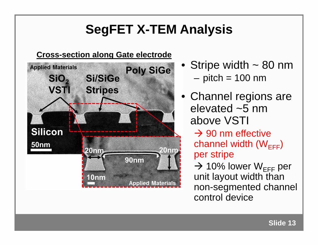
SegFET X-TEM Analysis
Slide 13
Cross-section along Gate electrode• Stripe width ~ 80 nm
– pitch = 100 nm
• Channel regions are elevated ~5 nm above VSTI 90 nm effective channel width (WEFF) per stripe 10% lower WEFF per unit layout width than non-segmented channel control device
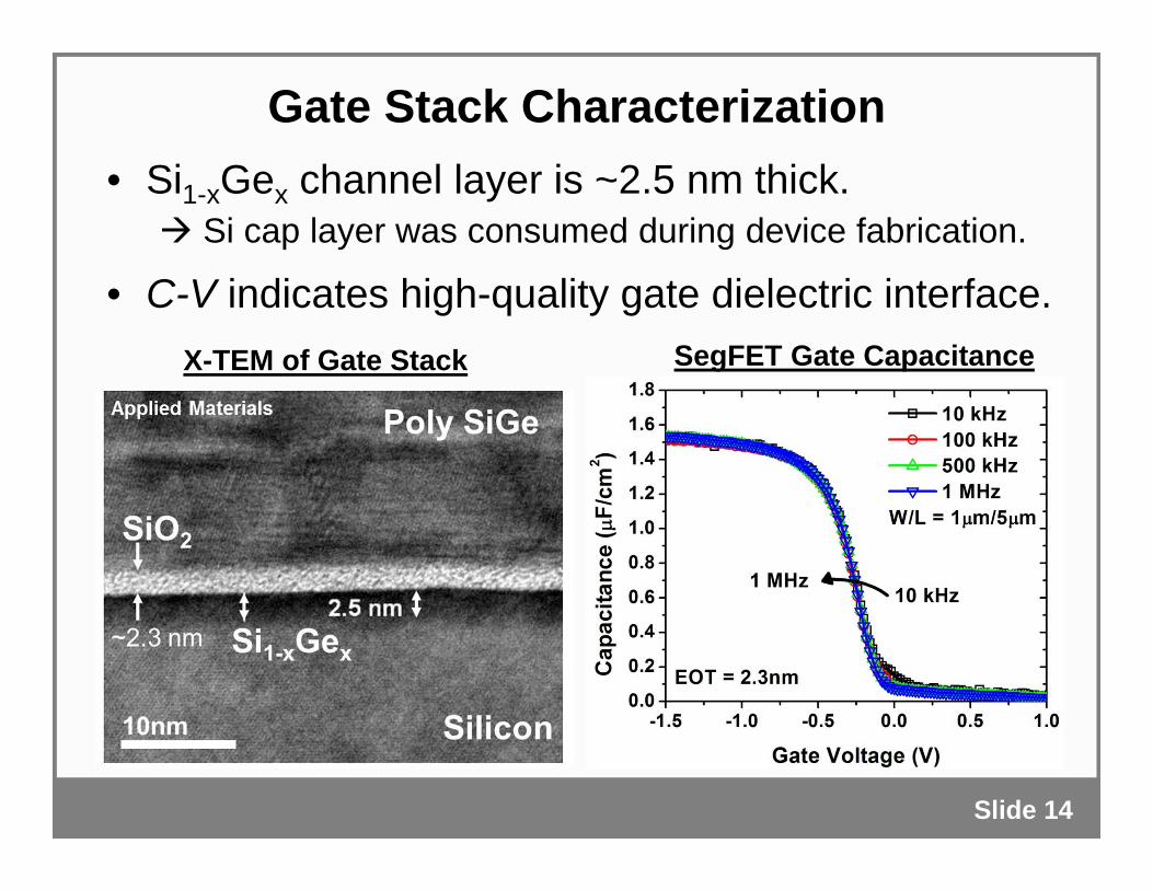
Gate Stack Characterization
Slide 14
• Si1-xGex channel layer is ~2.5 nm thick. Si cap layer was consumed during device fabrication.
• C-V indicates high-quality gate dielectric interface.SegFET Gate CapacitanceX-TEM of Gate Stack
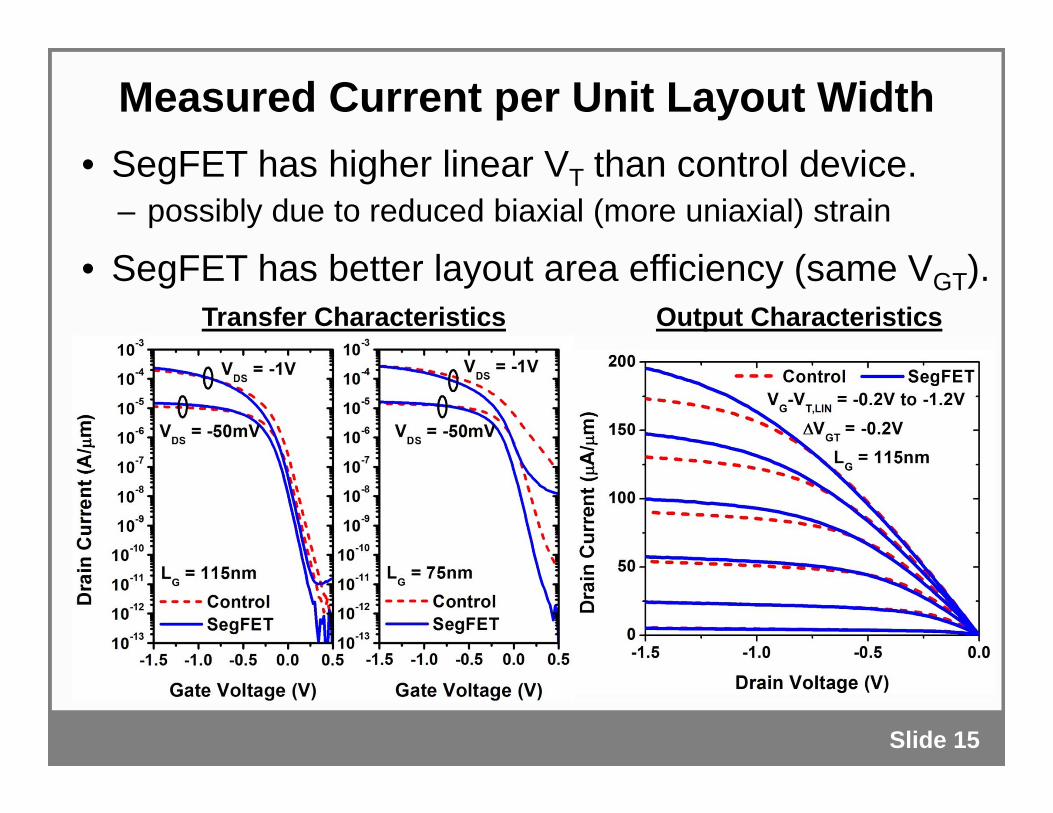
Measured Current per Unit Layout Width
Slide 15
• SegFET has higher linear VT than control device.– possibly due to reduced biaxial (more uniaxial) strain
• SegFET has better layout area efficiency (same VGT).Output CharacteristicsTransfer Characteristics
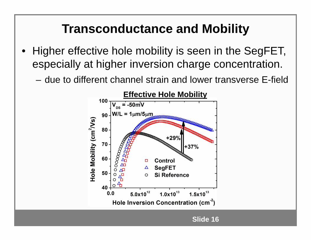
Transconductance and Mobility
Slide 16
• Higher effective hole mobility is seen in the SegFET, especially at higher inversion charge concentration.– due to different channel strain and lower transverse E-field
Effective Hole Mobility
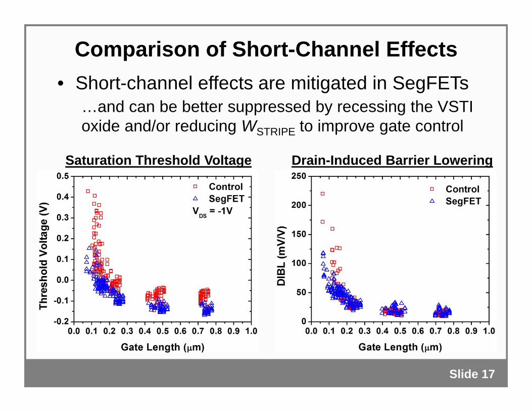
Comparison of Short-Channel Effects
Slide 17
• Short-channel effects are mitigated in SegFETs…and can be better suppressed by recessing the VSTI oxide and/or reducing WSTRIPE to improve gate control
Drain-Induced Barrier LoweringSaturation Threshold Voltage
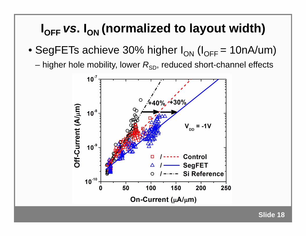
IOFF vs. ION (normalized to layout width)
Slide 18
• SegFETs achieve 30% higher ION (IOFF = 10nA/um)– higher hole mobility, lower RSD, reduced short-channel effects
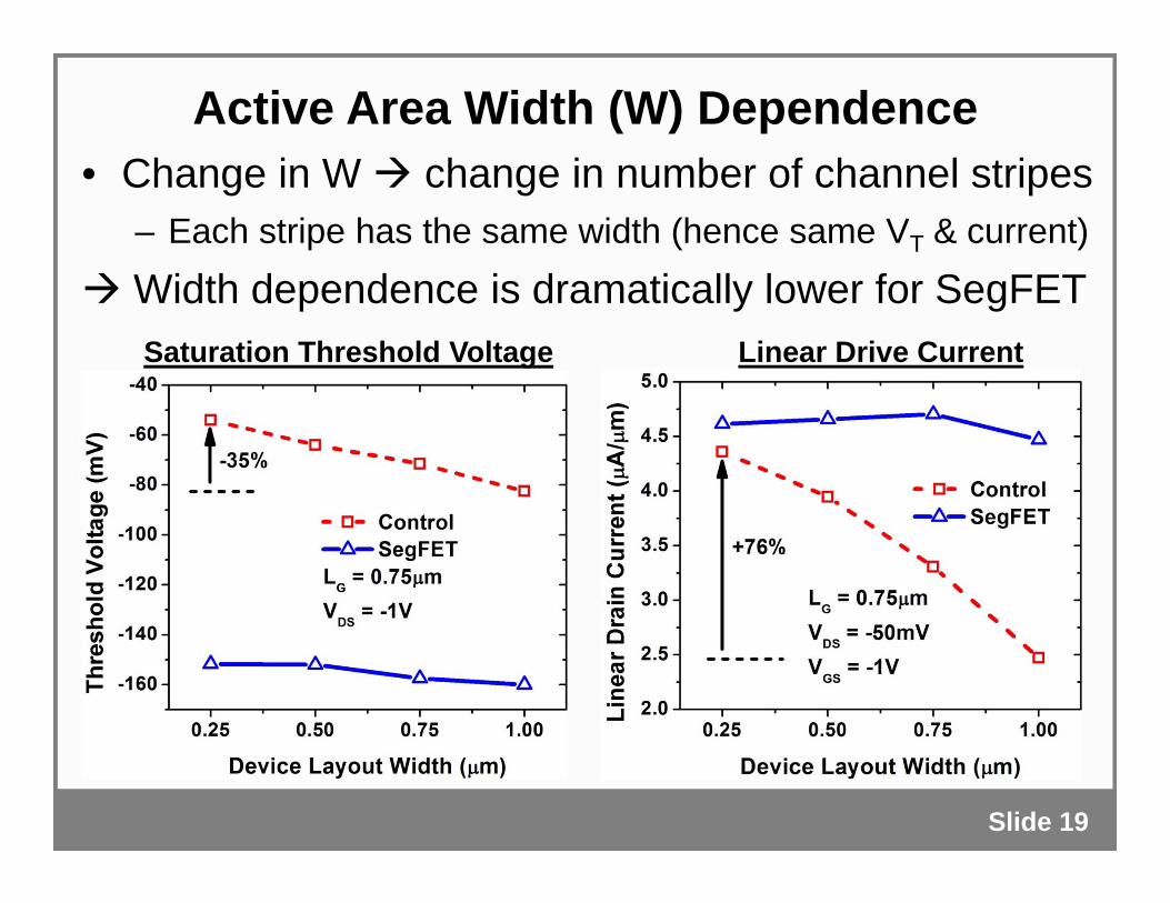
Active Area Width (W) Dependence
Slide 19
• Change in W change in number of channel stripes– Each stripe has the same width (hence same VT & current)
Width dependence is dramatically lower for SegFETSaturation Threshold Voltage Linear Drive Current
Outline• Introduction
– Why silicon-germanium (Si1-xGex) ?– Segmented-channel MOSFET (SegFET) design
• Device Fabrication– Corrugated substrate– p-channel MOSFETs
• Results and Discussion• Conclusion
Slide 20
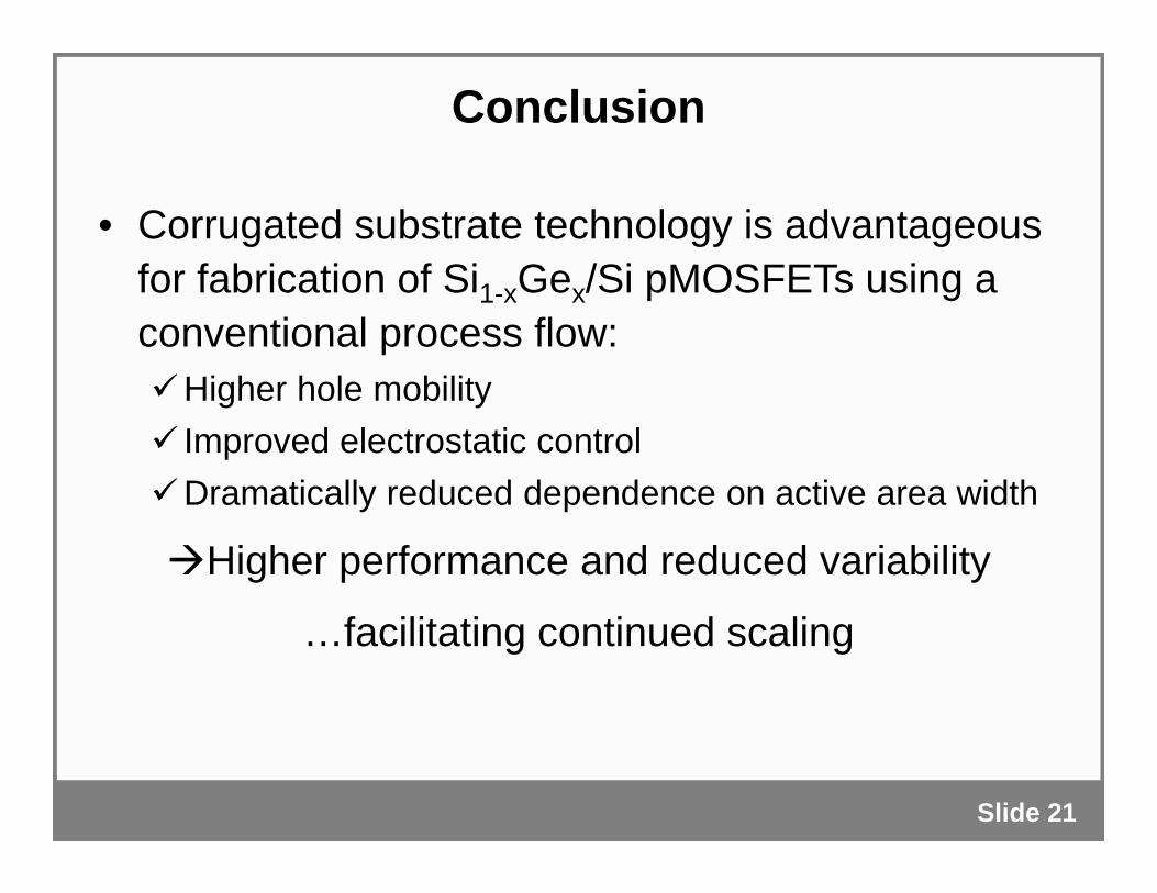
Conclusion
Slide 21
• Corrugated substrate technology is advantageous for fabrication of Si1-xGex/Si pMOSFETs using a conventional process flow:Higher hole mobility Improved electrostatic controlDramatically reduced dependence on active area width
Higher performance and reduced variability
…facilitating continued scaling
Acknowledgements
Slide 22
• Semiconductor Research Corporation– GRC Graduate Fellowship– Contract 2007-VJ-1631
• UC Berkeley Marvell Nanofabrication Laboratory