
SECTION 3 Additional Upgrades
20
SECTION 3 Additional Upgrades
Transcript of SECTION 3 Additional Upgrades

SECTION 3 Additional Upgrades


64K SIDEWAYS RAM DAUGHTER BOARD FITTING INSTRUCTIONS
These instructions are intended for use with the Acorn 64K upgrade board which may be fitted to the BBC microcomputer model B+. This upgrade should only be carried out by an Acorn authorised dealer and should not be attempted by members of the general public.
The upgrade kit should contain:
1. The 64K Sideways RAM Daughter Board2. Acorn 64K Sideways RAM Support Disc3. 1770 IFS4. Instructions for use
If any of these items are missing then you should contact your supplier.
To carry out this upgrade it is first necessary to dismantle the BBC microcomputer and remove the main PCB. Before removing the lid of any microcomputer ensure that it is not connected to the mains power supply.
When the PCB has been removed from the machine proceed as follows:
Modifications to the Main PCB.
1. On the solder side of the main PCB locate and cut the track that connects pin 13 to pin 14 of IC40. When cutting the track, take care not to damage the adjacent signal tracks on the PCB.
2. Locate and cut the track connecting to pin 10 of IC52.
Having completed the modifications, the daughter board may be fitted. The daughter board should be positioned such that the solder side of the daughter board is to the outside (adjacent to the case) of the machine. Insert the pins of the daughter board into position IC96, having previously cleared this position of any excess solder, and solder the board in place. Great care must be taken to ensure that the board is vertical. If the daughter board is permitted to lean towards the side of the case it will prevent the case lid from being fitted.
Having installed the daughter board, the 10 flying leads must be connected. With one exception (the Black lead) all the leads are routed around the rear of the daughter board and under the PCB, the solder connections to be made on the solder side of the main PCB. The Black lead travels over the component side of the main PCB and will be-connected by means of the shell housing already fitted to the lead.

The points to which the 10 leads must be connected are detailed in the table below.
WIRING CONFIGURATION TABLE
* The VIA hole to which the green lead must be connected is located next to pins 10 and 11 of IC63.
When all the connections have been made the PCB should be replaced inside the case and the machine should be reassembled.
Before replacing the lid replace the original 1770 DFS with the one supplied with the upgrade kit. This replacement is essential since the new DFS contains the utilities for use with the RAM upgrade.
Having completed the upgrade and replaced the lid, the upgraded machine should be tested.
A test routine is supplied on the support disc that accompanies the upgrade.
To run this test enter CHAIN "TEST" <RETURN> and when the > prompt reappears press the BREAK key. Upon completion of the test a pass or fail message will be displayed.
BBC MICROCOMPUTER MODEL B
1770 DISC INTERFACEUPGRADE KITFITTING INSTRUCTIONS

CONTENTS
Section Page
FOREWORD 3
1 INTRODUCTION 4
1.1 General 41.2 Component Location 41.3 Integrated Circuit Pin Numbering 41.4 Removal of an Integrated Circuit 51.5 Insertion of an Integrated Circuit 5
2 DISMANTLING PROCEDURE 5
3 PRINTED CIRCUIT BOARD CONFIGURATIONS 6
4 FITTING THE 1770 DISC INTERFACE MODULE 6
5 FITTING THE 1770 DISC FILING SYSTEM ROM 7
6 REASSEMBLY PROCEDURE 9
7 TESTING THE COMPUTER 9
8 PRINTED CIRCUIT BOARD MODIFICAT]KONS 10
FOREWORD
These upgrade instructions are for the use of persons fitting the 1770 Disc Interface Module to any issue of the BBC microcomputer Model B. This 1770 disc upgrade is NOT suitable for the BBC microcomputer model B+. The upgrade kit should contain the following component parts:
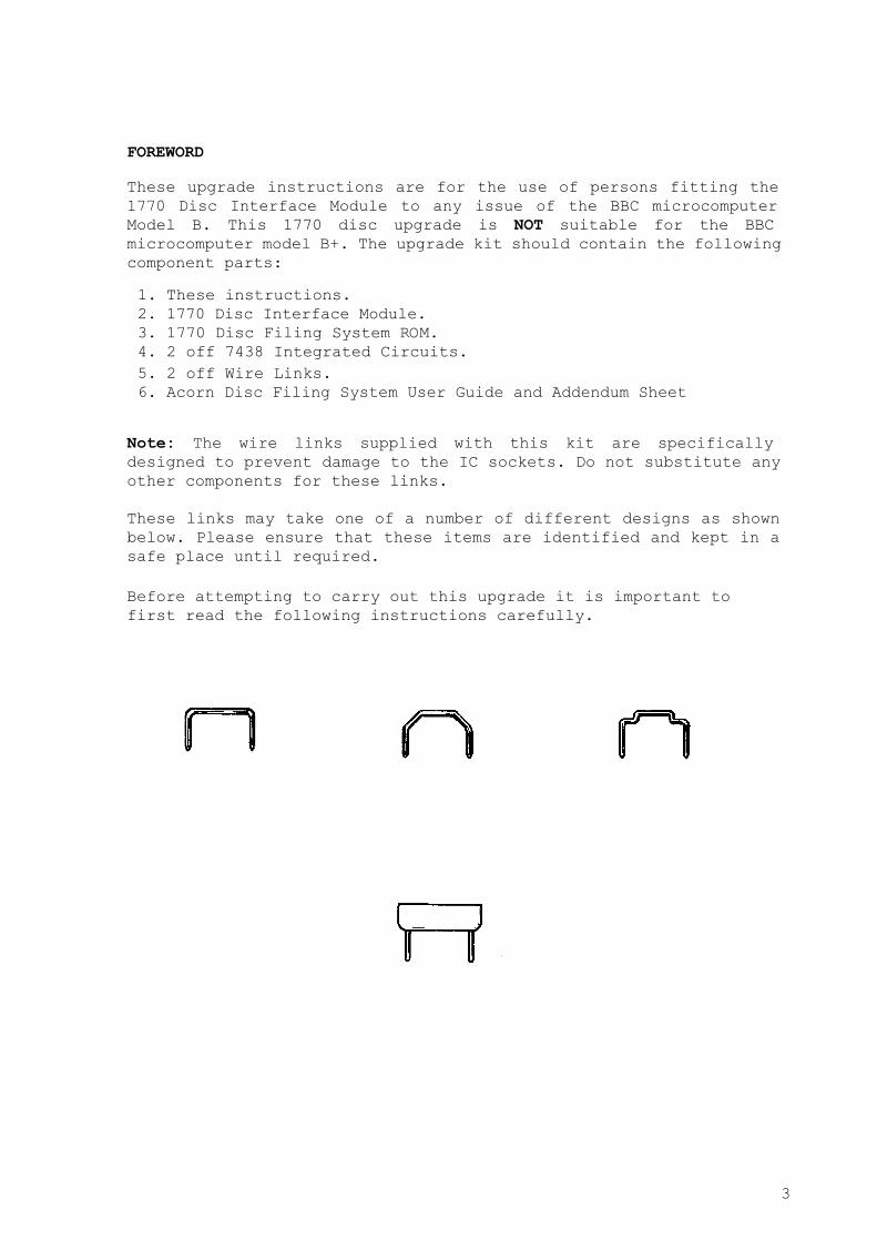
1. These instructions.2. 1770 Disc Interface Module.3. 1770 Disc Filing System ROM.4. 2 off 7438 Integrated Circuits.
5. 2 off Wire Links.6. Acorn Disc Filing System User Guide and Addendum Sheet
Note: The wire links supplied with this kit are specifically designed to prevent damage to the IC sockets. Do not substitute any other components for these links.
These links may take one of a number of different designs as shown below. Please ensure that these items are identified and kept in a safe place until required.
Before attempting to carry out this upgrade it is important to first read the following instructions carefully.
3

1 INTRODUCTION
1.1 General
The BBC microcomputer model B main Printed Circuit Board currently stands at Isuue 7. There should be no Issue 1 PCBs in the field, so these upgrade instructions will only cover upgrading Issues 2,3,4 and 7 (Issues 5 and 6 were never produced). There are no modifications required to the PCB for the Issue 4 and 7 boards, whereas Issues 2 and 3 may require modification. It is therefore important to identify the issue of the PCB before starting work. The issue number appears on the PCB in the silk screen legend just to the left of the board centre. If you look there you will see:
COPYRIGHT 1982 203,000 Issue X ACORN COMPUTERS Ltd
where X is the issue number.
1.2 Component location
It is necessary to understand the Acorn notation for locating a point on the PCB. This is done by considering the board as a compass. Position the PCB so that the components are facing upwards and the IDC headers (PLs 8,9,10,11 and 12) are closest to you. The edge furthest away from you (with the DIN sockets and modulator on it) is then NORTH, to your right is EAST, to your left is WEST and nearest is SOUTH.
1.3 Integrated circuit pin numbering
To install the 1770 module, an understanding of the pin numbering convention for integrated circuits is required.
With two exceptions, all ICs on the main PCB face NORTH, with pin one being located at the NORTH WEST corner of the chip. Pin one is indicated in one of two ways. Either a small dot or dimple is placed directly next to pin 1, or a half-moon shaped notch is cut into the pin 1 end of the IC, with pin 1 always being to the left of the notch when the notch is held uppermost. In some instances both of these indicators will be present.
Figure 1
4

The numbering sequence for a 14 pin device is shown in fig.l. As can be seen pin 1 is at the NORTH WEST corner, all the other pins are numbered consecutively in an anti-clockwise direction.
1.4 Removal of an integrated circuit
To avoid bending or breaking any pins, ICs must be removed very gently. Take a flat bladed screwdriver or similar tool and insert it between the body of the IC and the socket frame; gently prise up each end a bit at a time. Care must be taken to ensure that damage is not done to any PCB tracks that may be underneath the IC. Please note that frequent removal and insertion of an IC will inevitably lead to damage of both the IC and its socket.
1.5 Insertion of an integrated circuit
Before removing the IC from its protective packaging, identify pin1 (see section 1.3).
Before inserting the IC into the socket first check to see if the legs of the IC are parallel with each other. If they appear crooked or splayed apart then they should be realigned. To do this hold the IC sideways on and press it gently against a firm flat surface, repeat for the other side of the IC.
Hold the ends of the IC between thumb and forefinger, and line up all the pins over the destination socket. Pin 1 should face to the NORTH (see section 1.2).
Apply firm pressure to the IC, but do not force it. When the chip is in place it may appear to be slightly raised. Check that all the pins have entered the socket and that none are bent either outwards or under the body of the IC.
2 DISMANTLING PROCEDURE
Before starting to dismantle the computer, first ensure that the unit is disconnected from the mains supply.
Locate and remove the four case fixing screws (sometimes labelled FIX); two are located at the rear and two underneath at the front.
Remove the upper half of the case.
Locate and remove the keyboard securing bolts; taking note of the assembly order of the nut and various washers. There will be either two or three of these bolts depending on the issue of the machine.
Unplug the 17 way keyboard ribbon cable from the main PCB at PL13. Care shbuld be taken to ensure that the Molex strip at PL13 is not damaged.
Unplug the speaker lead from PL15.
5

If the Speech option is fitted to the machine, it will be necessary to unplug the 10 way ribbon cable from PL14.
The keyboard may now be removed from the machine.
3 PCB CONFIGURATIONS
Before commencing the upgrade it is necessary to check the following points. Check location IC 78 on the PCB for the presence of a 40 pin IC DIL socket. In the unlikely event that this socket is not present (either with or without the 8271 IC fitted), refer to section 8.
3.1 Check for the presence of a 14 pin IC DIL socket at location IC86. If a socket is not present, refer to section 8.
3.2 If the PCB is either an Issue 2 or an Issue 3, and a disc interface is not already installed, additional modifications are required, refer to section 8.
4 FITTING THE 1770 DISC INTERFACE MODULE
4.1 Locate link S9 which is located 1 inch to the WEST of pin 1 of IC78. If a wire link is fitted at this position, it must be cut using a small pair of wire cutters.
4.2 Locate ICs 79 and 80 which are situated directly to the SOUTH WEST of PL13 (the keyboard ribbon cable connector). If a disc interface was previously fitted to the machine, these two sockets will both contain ICs identified on top by the numbers 7438.
If a disc interface was not already fitted to the machine, these two ICs will be absent. In this instance insert the two 7438 ICs contained within the 1770 disc interface kit into these two sockets. Take care to follow the instructions on chip orientation and insertion contained within section 1.
4.3 Locate and remove the 8271 IC which is fitted at position IC78, the procedure for IC extraction is described in section 1.4.
4.4 If a socket is fitted at IC86, remove the 74LS393, taking care not to damage the socket or surrounding PCB.
Fit one of the wire links provided with the upgrade kit into socket IC86 connecting between pin 1 and pin 4 (see fig.2).
Locate position IC87. If this position is occupied by a 74LS123, the second link supplied with the upgrade should be disregarded. If the 74LS123 is not present the second link should be fitted between pins 9 and 12.
6
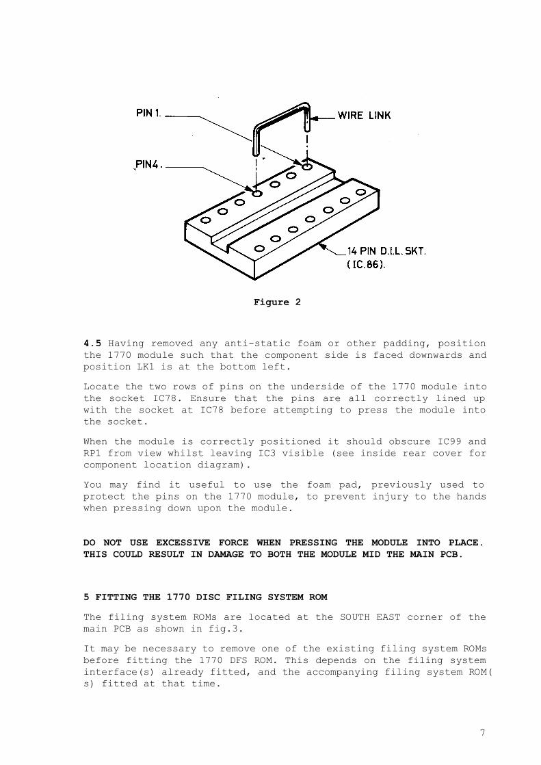
Figure 2
4.5 Having removed any anti-static foam or other padding, position the 1770 module such that the component side is faced downwards and position LK1 is at the bottom left.
Locate the two rows of pins on the underside of the 1770 module into the socket IC78. Ensure that the pins are all correctly lined up with the socket at IC78 before attempting to press the module into the socket.
When the module is correctly positioned it should obscure IC99 and RP1 from view whilst leaving IC3 visible (see inside rear cover for component location diagram).
You may find it useful to use the foam pad, previously used to protect the pins on the 1770 module, to prevent injury to the hands when pressing down upon the module.
DO NOT USE EXCESSIVE FORCE WHEN PRESSING THE MODULE INTO PLACE. THIS COULD RESULT IN DAMAGE TO BOTH THE MODULE MID THE MAIN PCB.
5 FITTING THE 1770 DISC FILING SYSTEM ROM
The filing system ROMs are located at the SOUTH EAST corner of the main PCB as shown in fig.3.
It may be necessary to remove one of the existing filing system ROMs before fitting the 1770 DFS ROM. This depends on the filing system interface(s) already fitted, and the accompanying filing system ROM(s) fitted at that time.
7

Inserting ROMS — BBC Microcomputer Model BThis diagram shows a plan view of the BBC Microcomputer Model B. The top of the computer casing has been removed to reveal the four sideways ROM sockets. ROM software may be inserted in any of these sockets.
Figure 3
The options are:
ROM type Filing system(s) already fitted Action to be taken
0.90 DFS DISC ONLY Replace with 1770 DFS ROM.
0201,666-01 Replace with 1770or DISC ONLY DFS ROM. 3.0 DNFS
As above ECONET ONLY ADD 1770 ROM to spare socket.
As above DISC and ECONET ADD 1770 ROM to spare socket.
2 ROMs : Replace 0.90 DFS0.90 DFS DISC and ECONET with 1770 ROM.and Leave 3.34 NFS3.34 NFS fitted.
For instruction on removal and insertion of ROMs or any other IC please refer to sections 1.4 and 1.5.
8

6 REASSEMBLY PROCEDURE
When the upgrade has been completed the unit should be reassembled as follows:
6.1 Ensure that no foreign objects are left inside the unit since they may cause shorting and damage to the unit after reassembly.
6.2 Reconnect the speaker lead to PL15
6.3 Reconnect the 17 way keyboard ribbon cable to PL13 taking care to ensure that the socket is correctly positioned (it is easy to offset the socket on the plug either one pin to the right or to the left).
6.4 If the Speech option is fitted, the 10 way ribbon cable must be connected to PL14. Care must again be taken to ensure that the socket is not offset on the plug.
6.5 Relocate the keyboard securing bolts and replace the washers and nuts in the correct order.
6.6 Replace the upper half of the case, relocate the four fixing screws and tighten them securely.
6.7 Check the working area to ensure that all components have been refitted to the unit and that nothing has been overlooked.
7 TESTING THE COMPUTER
When the upgrade has been completed and the unit has been reassembled connect the computer to a compatible disc drive in the manner described in the Acorn Disc Filing System User Guide.
Following the instructions contained within the Acorn Disc Filing System User Guide, prepare a disc for use and then attempt to load and save programs to and from the disc. If these operations can be carried out satisfactorily, it may be assumed that the upgrade was successful and that the disc interface is working correctly.
Any dealer performing this upgrade should test the completed unit using the Acorn PORT tester.
NOTE: Some pieces of commercial software may not function when used in conjunction with the 1770 disc interface. This is due to the nature of the protection employed by certain software houses. If this is the case then advice should be sought from the software supplier.
9

8 PRINTED CIRCUIT BOARD MODIFICATIONS
!WARNING PLEASE READ IN FULL!
THIS SECTION IS INTENDED FOR THE USE OF ACORN DEALER SERVICE PERSONNEL. MEMBERS OF THE PUBLIC SHOULD NOTE THAT ANY MODIFICATIONS CARRIED OUT TO THE PRINTED CIRCUIT BOARD OF ANY ACORN EQUIPMENT IS UNDERTAKEN AT THE SOLE RISK OF THE PERSON CARRYING OUT THE MODIFICATION. NO CLAIM FOR LOSS OR DAMAGE TO THE MICROCOMPUTER CAUSED THROUGH THE MODIFICATION OF THE PRINTED CIRCUIT BOARD BY UNQUALIFIED PERSONNEL SHALL BE ACCEPTED BY ACORN COMPUTERS LIMITED.
PLEASE READ ALL INSTRUCTIONS CAREFULLY. IF YOU ARE IN DOUBT ABOUT YOUR ABILITY TO CARRY OUT THE NECESSARY MODIFICATIONS, THE 1770 DISC UPGRADE MODULE, AND THE BBC MICROCOMPUTER SHOULD BE TAKEN TO YOUR NEAREST AUTHORISED ACORN DEALER.
A CHARGE MAY BE LEVIED BY THE DEALER FITTING THIS UPGRADE TO YOUR BBC MICROCOMPUTER; SUCH A CHARGE SHALL BE ENTIRELY AT THE DISCRETION OF THE DEALER CONCERNED.
10

8.1 Removing the main printed circuit board
Having removed both the upper half of the case and the keyboard assembly proceed as follows:
Disconnect the seven flying leads connecting the computers power supply to the main PCB, 3 red, 3 black and 1 purple.
Disconnect the two leads connecting the composite video socket (SK2) to the PCB.
Locate and remove the four (sometimes five or seven) PCB securing screws; two of which are situated on the SOUTH edge, one in the NORTH WEST corner and one in the NORTH EAST corner of the PCB.
The PCB may now be removed from the case by sliding it forwards and then lifting it from the rear.
Upon completion of all the necessary modifications, the PCB should be refitted by following the reverse of the above procedure. Having refitted the PCB the upgrade should be completed by following the procedure detailed in section 4.
8.2 Modification required when fitting a disc interface to an Issue 2 or 3 PCB
If the machine is fitted with an Issue 2 or 3 PCB then the following modification must be performed.
On the component side of the PCB, locate and cut the track connected to pin 9 of 1027. This cut should be made as close to 1027 as possible.
Locate and cut pin 9 of 1027. The cut should be made as close to the PCB as possible. If 1089 is fitted then its temporary removal will make this operation easier.
Bend pin 9 of 1027 into a horizontal position.
Solder a piece of insulated wire between pin 9 of 1027 and the EAST pad of link S9.
NOTE: Excercise extreme caution when making solder joints. Damage may easily be done to the IC when performing this operation.
8.3 Modification required where a socket is not fitted at position IC 86
There are three possible options:
1. Remove the PCB as detailed in section 8.1. Desolder and remove 1086 and fit a 14 pin DIL IC socket at position 1086. The upgrade may then be performed as described in section 4.
11

Figure 4
12
2. Remove the PCB as detailed in section 8.1. Locate and cut LK1 on the 1770 module. Using a piece of insulated wire, connect the pad of LK1 (indicated with an 'X' in fig.4), to the plate through hole directly to the NORTH of pin 1 of IC86 (see assembly diagram on inside back cover).
3. Locate and cut LK1 on the 1770 module. Using a piece of insulated wire, connect the pad of LK1 (as detailed in 2 above) to pin 1 of IC86.
If either option 2 or option 3 is used, the procedure detailed in section 4.1 is not required. If option 1 is used then section 4.1 still applies.
Option 3 is not recommended due to the likelyhood of damage to the IC. Option 1 or 2 should be used in preference.
8.4 Modification required where a 40 pin DIL socket is not fitted at position IC78
Remove the PCB as detailed in section 8.1
Desolder and remove, where fitted, the 8271 disc controller IC.
Fit a 40 pin DIL IC socket at position IC78. Do NOT attempt to solder the 1770 disc interface module directly to the printed circuit board.
8.5 Upon completion of the appropriate modification(s), complete the installation of the upgrade as detailed in section 4.0.

MAIN PCB COMPONENT LAYOUT