Sebastian Bartlett, Josh Noel Professors Hom, Steinmeyer ...
87
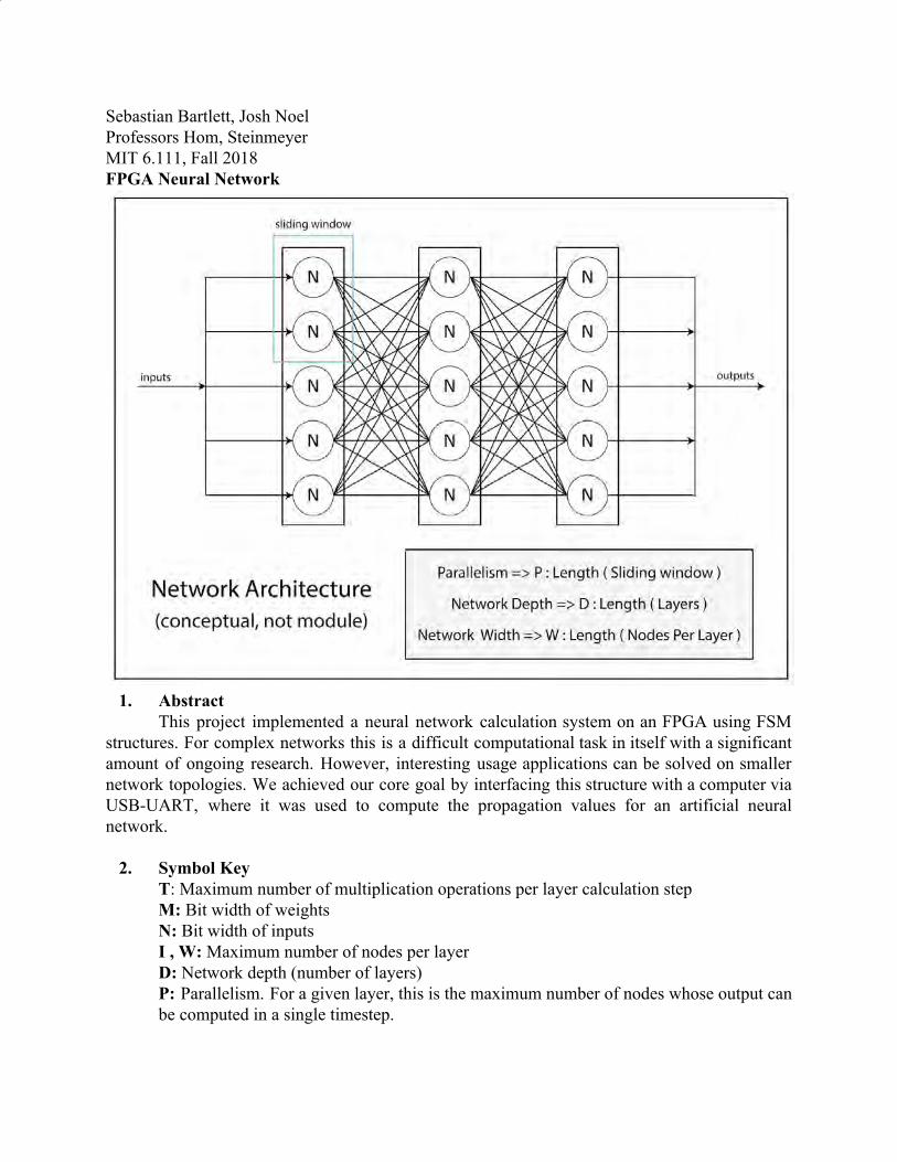
Sebastian Bartlett, Josh Noel Professors Hom, Steinmeyer MIT 6.111, Fall 2018 FPGA Neural Network 1. Abstract This project implemented a neural network calculation system on an FPGA using FSM structures. For complex networks this is a difficult computational task in itself with a significant amount of ongoing research. However, interesting usage applications can be solved on smaller network topologies. We achieved our core goal by interfacing this structure with a computer via USB-UART, where it was used to compute the propagation values for an artificial neural network. 2. Symbol Key T : Maximum number of multiplication operations per layer calculation step M: Bit width of weights N: Bit width of inputs I , W: Maximum number of nodes per layer D: Network depth (number of layers) P: Parallelism. For a given layer, this is the maximum number of nodes whose output can be computed in a single timestep.
Transcript of Sebastian Bartlett, Josh Noel Professors Hom, Steinmeyer ...
Sebastian Bartlett, Josh Noel Professors Hom, Steinmeyer MIT 6.111, Fall 2018 FPGA Neural Network
1. Abstract
This project implemented a neural network calculation system on an FPGA using FSM structures. For complex networks this is a difficult computational task in itself with a significant amount of ongoing research. However, interesting usage applications can be solved on smaller network topologies. We achieved our core goal by interfacing this structure with a computer via USB-UART, where it was used to compute the propagation values for an artificial neural network.
2. Symbol Key
T: Maximum number of multiplication operations per layer calculation step M: Bit width of weights N: Bit width of inputs I , W: Maximum number of nodes per layer D: Network depth (number of layers) P: Parallelism. For a given layer, this is the maximum number of nodes whose output can be computed in a single timestep.
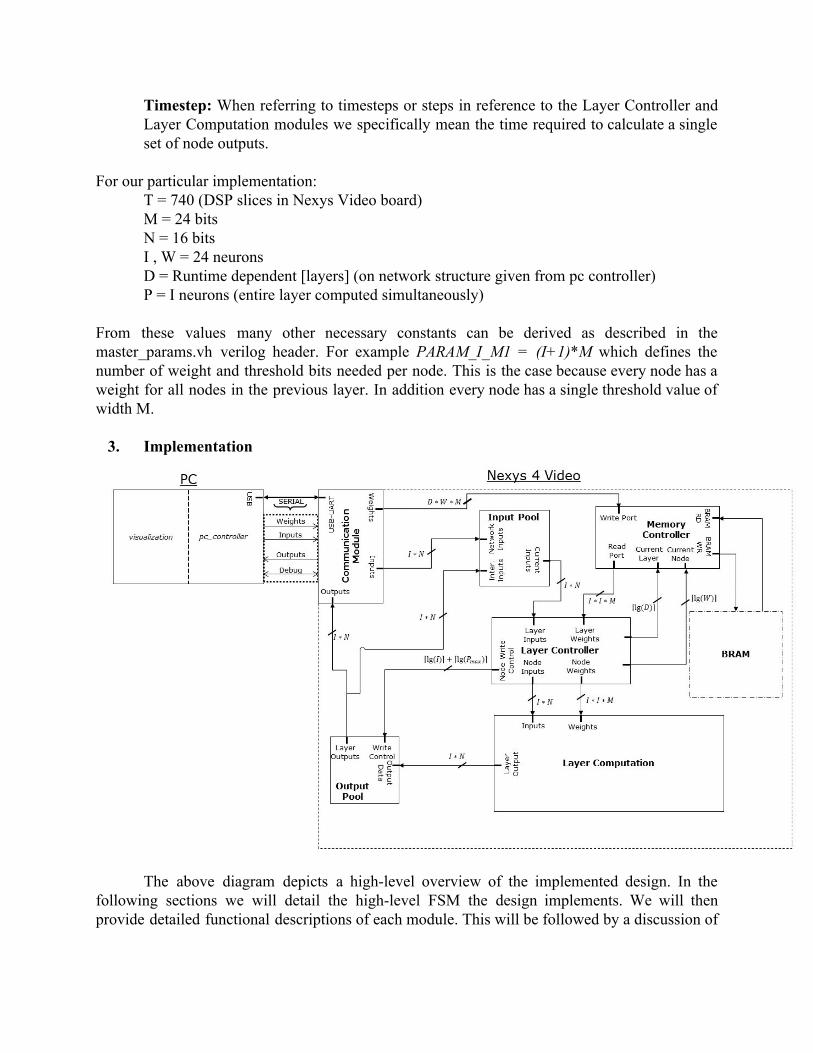
Timestep: When referring to timesteps or steps in reference to the Layer Controller and Layer Computation modules we specifically mean the time required to calculate a single set of node outputs.
For our particular implementation:
T = 740 (DSP slices in Nexys Video board) M = 24 bits N = 16 bits I , W = 24 neurons D = Runtime dependent [layers] (on network structure given from pc controller) P = I neurons (entire layer computed simultaneously)
From these values many other necessary constants can be derived as described in the master_params.vh verilog header. For example PARAM_I_M1 = (I+1)*M which defines the number of weight and threshold bits needed per node. This is the case because every node has a weight for all nodes in the previous layer. In addition every node has a single threshold value of width M.
3. Implementation
The above diagram depicts a high-level overview of the implemented design. In the following sections we will detail the high-level FSM the design implements. We will then provide detailed functional descriptions of each module. This will be followed by a discussion of

our visualization and testing frameworks along with a performance analysis of our final implementation.
3.1. State Machine
The diagram above describes the implemented FSM which computes the outputs of a multi-layer network on the FPGA. We begin in the weight_transfer communication state. In this state the weights for the entire neural network (in this case a single layer) are sent across the USB-UART interface from the PC to the FPGA Communication Controller module. The FPGA then stores these weights through the Memory Controller module. Along with these weights additional network topology information is sent. This currently includes the layer’s parallelism, “P”, and maximum node index.
Once all network information is transferred successfully, we enter the input_transfer state. In this state the network input layer values are sent to the FPGA via the UART interface in a similar fashion to the weights. These inputs are then stored in the Input Pool module as opposed to the Memory Controller module.
When all values for the input layer have been transferred, we begin the network_compute step. This state contains the bulk of our logic and computation. The parallelism “P”, discussed earlier, defines the number of nodes that can be computed in parallel for a given layer. In order to perform parallel computation of the forward propagation values for a given set of active nodes, the Layer Controller module reads in the appropriate inputs from the Input Pool and weights from the Memory Controller, and forwards these values to the Layer Computation module. The number of nodes that can be computed in parallel “P” is given by the expression T / I, where T represents the total number of DSP multipliers, and I represents the number of inputs to any given node in the layer. After this computation is complete, the outputs are written to the output pool. When multiple layers are being computed we signal a transfer from the output pool to input pool and computation restarts. When all final layer outputs are in the output pool, the layer controller signals a transition to the output_transfer state.
In the output_transfer state, the communication module reads the layer’s outputs from the output pool, and sends them to the PC as described in the protocol section. Upon reception of all output data the pc_controller can begin using the outputs received.
3.2. Communication Protocol (Josh)
3.2.1. Overview
In order to perform inference on the FPGA we must have the ability to transfer data between the Host PC and FPGA. A common protocol is shared between the PC and FPGA in order to encode all the necessary data. Specifically, we have a process running on a computer that feeds network topology information, including weights, and network inputs to the FPGA. This process is referred to as the pc_controller. On the FPGA side the communication_module receives this information and decodes it for use. The module also handles the transfer of network outputs back to the PC.
Our serial communication protocol has two actors: a sender and a receiver. For the weight_transfer and input_transfer states, pc_controller is the sender and the communication_module is the receiver. The roles are reversed in the output_transfer state.
3.2.2. Packet Streams
The protocol itself is defined as follows. All data is sent as a packet stream. A stream is defined to be 1 header packet and 9 data packets where a packet is a single byte. This stream abstraction allows for data to be sent in indepent chunks, and any data that would span multiple chunks is sent across multiple packet streams. Note that any leftover space in a packet stream after data insertion is zero-padded. The decision to make the packet stream 10 packets or 80 bits is that it aligns well with out weight bit-width of 24 bits and input/output bit-width of 16 bits. Excluding the header, there are 72 data bits per stream. This means that a single stream can contain 3 weight values with no wasted space or overflow. For inputs there is an overflow of 8 bits per stream (72 data bits % 16 bit input/outputs = 8 bits). This slight overlap does not add much complexity to input encoding as all data can still be handled on a byte-level granularity.
3.2.3. Packet Stream Headers

Header packets contain metadata for the packet stream as a whole. The first 2 bits specify
the mode for the following data packets. The supported modes are, weight, input, output, and debug. The next bit is whether CRC data for the stream should be expected immediately after the stream ends . The final 5 bits may contain additional metadata dependent on the mode of the 1
stream. Mode 0 is weight transfer mode, which indicates the data packets are weight packets. The
mode dependent header data is the layer id of the weights. Note that the communication protocol for weight transfer contains additional requirements so network metadata can be sent as data packets. Specifically, in the first packet stream for each layer (i.e. whenever the layer id portion of the weight header changes), the first 6 data packets must be the parallelism and maximum node id for the layer respectively. Note that 3 data packets per information is 24-bits the same width as a weight. This ensures that no special encode or decode logic must exist to locate this data within a stream, however the pc_controller and communication_module must know to treat the first two “weights” for each layer specially. In addition the first actual weight for every node is the node’s threshold rather than a weight connecting it to the previous layer.
Mode 1 is input transfer mode and mode 2 is output transfer mode. These types contain the same data, however in input transfer mode data flows from pc_controller to communication_module and in the opposite direction in output transfer mode. In this mode the dependent data is just zeroed. The input packets flow PC to FPGA and output packets from FPGA to PC.
Mode 3 is debug mode, indicating debug packets which are used to transfer debug data from FPGA to PC. In this mode the dependent data is an error code. Different error codes define different interpretations of the debug data packets.
As described in annotation 1, crc check is currently disabled, however this the protocol still defines its use as follows. If CRC_EN=1 every packet stream will be followed by a corresponding CRC bit sequence. This sequence will be checked on the receiver by recalculating the CRC of the concatenation [packet_stream, CRC]. If this does not yield 0 an ERROR header packet is sent. Otherwise a SUCCESS packet is sent (All 0 bits). Note that this means communication with CRC_EN=1 is necessarily two-way as confirm messages must be sent from
1 Note that the CRC_EN bit is always disabled in our current implementation as we did not encounter any errors during data transfer. However, the bit was left as it allows for easy extension in the future if some error correction must be implemented.

the receiver after every packet stream from the sender. Note that an LED on the FPGA is lit if any CRC error is detected or error packet received. If any error packet is received by the sender, it restarts transmission of the current state from the beginning.
3.3. Communication Module (FPGA) This module will implement the FPGA end of the communication protocol described
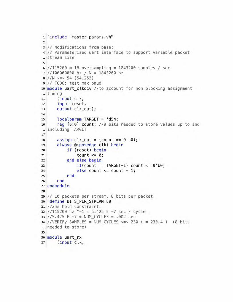
above. The input will be the TXD port (C4) of the FTDI FT232R USB-UART bridge. The output is the RXD port (D4). This module will operate at 115,200 baud. Note that the FT232R bridge is rated for up to 12MBaud, but we used a lower baud rate to simplify debugging as well as to better demonstrate the performance implications of a high communication overhead. These implications will be discussed further in section 7.
The implementation is similar to Lab 2B and Lab 5C. For this reason the uart interface was abstracted away in the modules uart_rx and uart_tx for receiving and transmission respectively. uart_rx was Sebastian’s Lab5C module modified to buffer an entire packet stream before sending it for decode. uart_tx was based on lab2b, but it takes in a packet stream and transmits at the necessary baudrate. Note that the 16x supersample clock generator was also abstracted into the uart_clkdiv module. The communication_module itself handles the decoding and encoding of packet streams for the previously described uart interfaces.
For decoding weight streams, every 3 data packets are combined to form a single 24-bit weight. The current layer_id is extracted from the header and also output from this module. The module must keep some state regarding the last layer received in order to decode the network metadata described in the communication protocol section. If it detects that it has received the first packet stream for a new layer, it will treat the first two weights as the layer’s parallelism and maximum node id respectively. These values are stored into output registers and sent to the parallelism_pool and max_node_id_pool. Note that the fact the first weight per node is a threshold is completely ignored by the communication module to cut down on complexity. It simply assumes every node has I+1 weights. Once all weights for a single node are received the communication module asserts a signal that the weight buffer is full. This signal is handled by the memory controller as described in section 3.4. This process continues as long as weight packets are received.
Input decoding is much simpler than weight decoding. Even though a single input may span multiple packet streams, all streams are buffered contiguously in the ordered received. This places the split input bytes consecutively. The communication module expects I inputs, so once it receives this many it asserts to the input pool that it should read the input buffer.
Note than sending an invalid number of weight or input bits such that it only partially fills the communication module weight or input buffer is disallowed by the communication protocol.
Once a debug packet with all 0 data packets is received, the communication module asserts that transfer in is completed and the layer controller begins working.
This module will also handle the sending of output data from the FPGA to the computer once the layer_controller asserts that the last layer’s outputs are in the output pool. These outputs will be read from the output pool, translated to packet streams, and each stream is then sent through uart_tx.
The main lesson learned through this project is in regards to this module. As I was testing communication it would have been very useful to create a test that combined only this module with the memory controller and input pool, and then used this test actually integrated with the

computer. I wrote a test similar to this clsoer to the end of the project that would simply send back to the computer the weights or inputs it had received. This tests not only the communication and decoding aspect, but also it’s interaction with the elements it needs to store persistent data to. This exposed a couple of bugs that would have been nice to find much earlier in the process. My main takeaway from this experience is to begin testing modules closer to the the environment they will be used in as soon as possible rather than relying on tests in isolation to prove correctness of the system as a whole.
3.4. Memory Controller (Josh) As we have defined our maximum network width and depth we can derive how much
memory is needed for the storage of weights. As described in the symbol key, we have a maximum network width of 24 and depth of 4. Every node has 24 weights + 1 threshold worth of bits to store through the memory controller. Multiplying all of this by a weight width of 24-bits yields:
57,600 bits4weightwidth 24netwidth netdepth 24netwidth threshold))2 * ( * 4 * ( + 1 =
The Nexys Video has 13 MBits of fast BRAM, so this is well within the limitations of the
board. As described in section 3.2, the communication module sends the weights and thresholds a single node at a time (I weights + 1 threshold). This yields a write port width of:
4weightwidth (24netwidth ) 00 bits2 * + 1 = 6
We synthesized a BRAM IP core with this port width, and depth defined as the maximum
number of nodes in a network. In regards to the memory controller implementation itself it has two distinct operating modes: writing and reading.
For writing the memory controller keeps an internal counter tracking the number of nodes that have been written so far. It then writes to this index in BRAM. The resulting memory layout is such that any reads will be from consecutive indices, as all nodes within a layer will have been stored one after another.
For reading the layer computation module expects to receive weights and thresholds for P (parallelism) nodes in the current layer. For this reason two output shift registers are created read_weights and read_thresholds. In order to read all necessary values from memory, a single layer read request is broken up into a BRAM read request for P nodes in the layer. The initial read address is calculated from the signals read_layer_id and read_node_id. Since data is written layer-by-layer we can reconstruct the start index for a given layer and node as:
read_layer_id*MAX_NET_WIDTH + read_node_id Once a single node read response is returned from BRAM, the first weight is shifted into
the output threshold shift register and the remaining weights shifted into the output weight shift register. P defines the parallelism of the current layer, but if MAX_NET_WIDTH % P != 0 then it is possible that less than P reads must be done for the final nodes in a layer. For this reason the layer controller checks the current node id being read against the maximum node id for the layer. Note that this id verification functionality is not needed in the current implementation given that
we have enough DSP slices to support calculating an entire layer per computation step. Thus, P will never cause a read past max_node_id as P = LayerWidth. Once all consecutive BRAM reads are completed the output shift registers are full and a read_rdy signal is asserted.
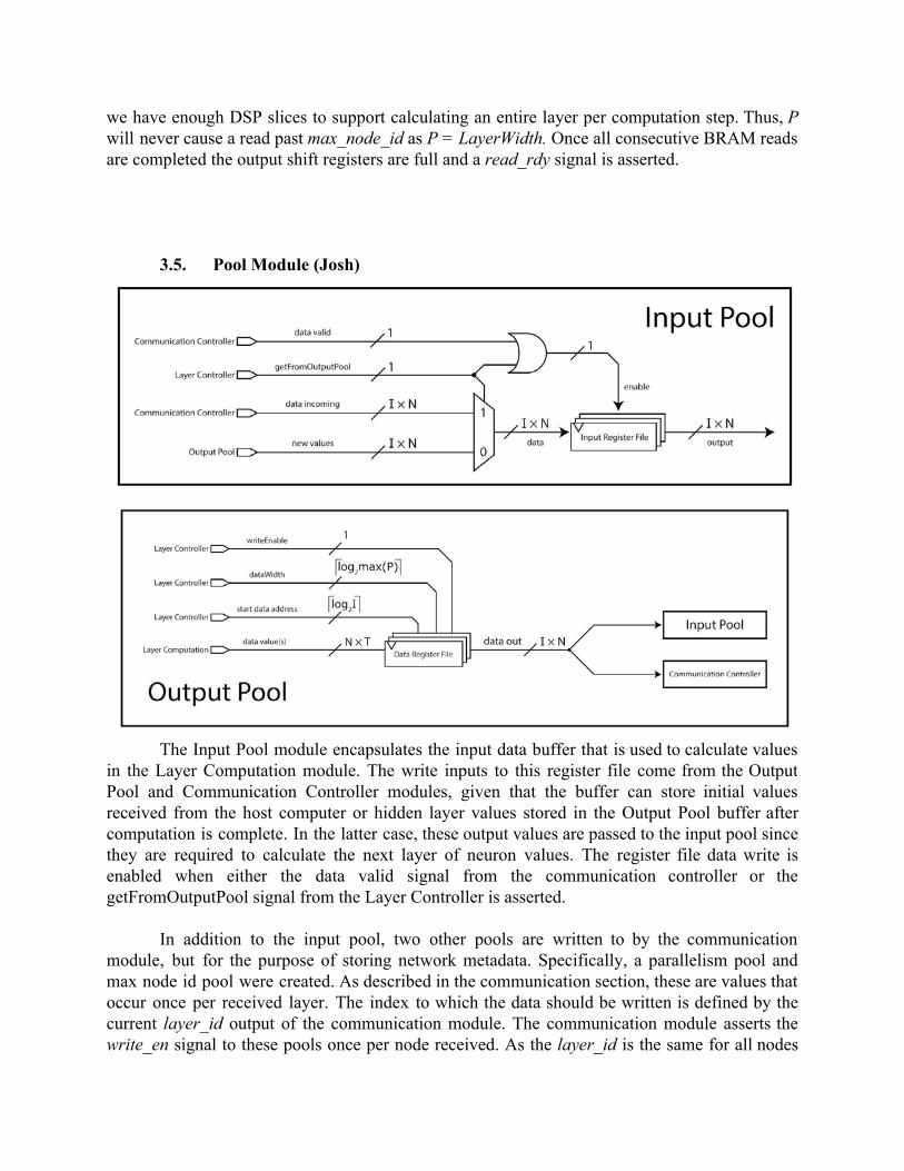
3.5. Pool Module (Josh)
The Input Pool module encapsulates the input data buffer that is used to calculate values
in the Layer Computation module. The write inputs to this register file come from the Output Pool and Communication Controller modules, given that the buffer can store initial values received from the host computer or hidden layer values stored in the Output Pool buffer after computation is complete. In the latter case, these output values are passed to the input pool since they are required to calculate the next layer of neuron values. The register file data write is enabled when either the data valid signal from the communication controller or the getFromOutputPool signal from the Layer Controller is asserted.
In addition to the input pool, two other pools are written to by the communication
module, but for the purpose of storing network metadata. Specifically, a parallelism pool and max node id pool were created. As described in the communication section, these are values that occur once per received layer. The index to which the data should be written is defined by the current layer_id output of the communication module. The communication module asserts the write_en signal to these pools once per node received. As the layer_id is the same for all nodes

in the same layer, multiple writes of the same data occur for every layer, but this has no negative effects. To read from these pools the index input is used to extract a value from the internal buffers and store it in an output register. Reads are initiated by the layer controller in order to read from memory controller as this module needs to know the parallelism and maximum node id of the layer being read.
The Output Pool serves as the buffer for Layer Computation outputs. As opposed to the Input Pool, which modifies the entire register file on a write operation, the output pool uses the data start address and data width values from the Layer Controller to determine which registers to write to when writeEnable is asserted. This occurs because the output pool was designed to allow for partial computation of layers where some outputs will be sent after one computation step, and the rest of the outputs will be sent across some number of computation timesteps. Note, however, that although the output pool supports this functionality, the rest of the system currently always calculates a full layer per computation step. This change occurred as with the increased number of DSP slices on the Nexys Video, we had enough multipliers to do so. The data from this register file is forwarded to the Input Pool upon layer computation completion and the Communication Controller once all layers finish.
3.6. Layer Controller (Sebastian)
The Layer Controller module acts as the primary control FSM for calculating the neural
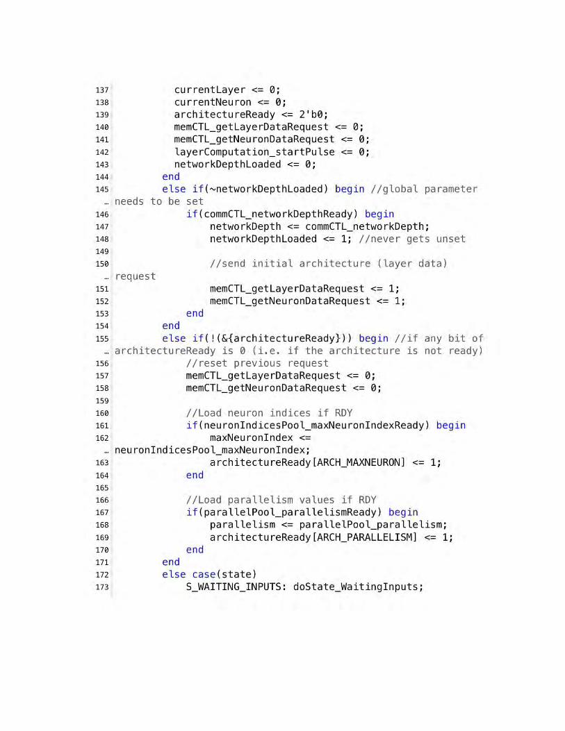
network layers. To begin, the network depth is loaded from the Communication Controller via the commCTL_networkDepth bus and corresponding ready signal. During this data latching the requests for layer architecture data and neuron weight data for the primary layer are initiated via memCTL_getLayerDataRequest and memCTL_getNeuronDataRequest signals. These values are latched once the requests have valid data on their respective buses and active ready signals. The Layer Controller then waits until the Input Pool has neuron input data ready for calculation, which forms the S_WAITING_INPUTS state of the FSM. Once these conditions are met, the Layer Controller sends a pulse to the Layer Computation module (layerComputation_startPulse) to initiate the calculations for the layer. The Layer Controller FSM waits for the layer computation to finish (state S_WAITING_LAYERCOMP ), and if the current layer being considered is the last layer, a signal is asserted for the communication controller to fetch data outputs from the Output Pool (commCTL_isStateDone ). If the layer being processed is an intermediate ("hidden") layer, the layer counter is incremented, and requests for the next layer architecture and neuron weights are sent to the memory controller. The FSM then returns to the input waiting state as previously delineated.
As inputs, the Layer Controller receives the network depth, parallelism values, maximum neuron index for the given layer, as well as flags from other modules indicating the ready status of weights, inputs, and valid data outputs. The Layer Controller outputs the data ready signal to the Input Pool so that values are cycled from the Output Pool, parameters for the Memory Controller to fetch the appropriate data values, request signals to assert data fetch, as well as flags to the Communication Controller and Layer Computation modules regarding data-flow validity and timing, respectively.
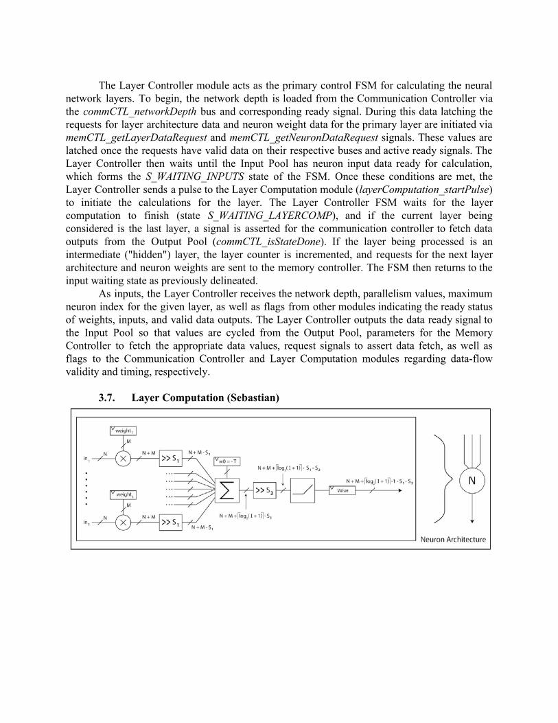
3.7. Layer Computation (Sebastian)

The Layer Computation module serves as the central data processor for the project. The inputs of this module include the incoming weights, thresholds, and inputs for the neurons in the current layer of computation, as well as a start pulse from the Layer Controller. To begin, the set of weights and inputs are multiplied in pairs, effectively calculating the dot product between the two value vectors. These values are then right shifted by a quantity “S1”, in order to reduce the

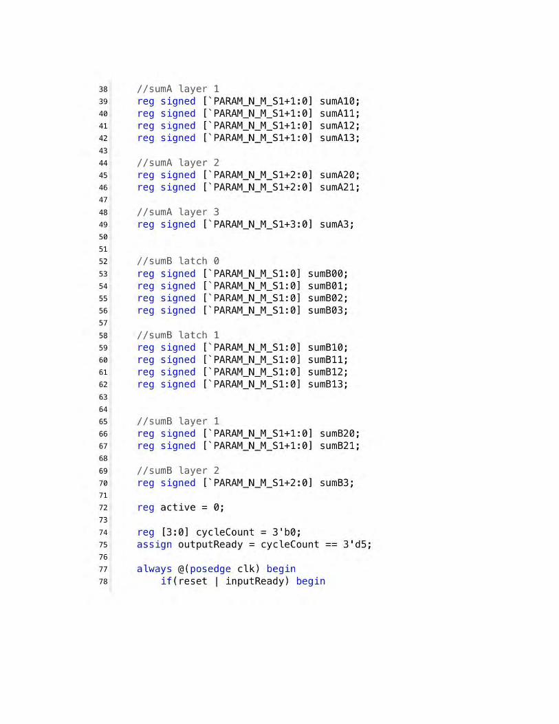
hardware needed for summation as well as reduce the probability of an overflow result. The results of this shift are stored in the multiplicationResult bit array. The values are then added together using an array of one tree adder per neuron TreeAdder24(0-23), and then right shifted by another quantity “S2” to reduce the bit width of the output values to be the same as the input values, given the cyclic implementation of calculating layers in this hardware implementation. Once all values are computed, they are sent to the Output Pool for further data routing along with an enable signal to indicate that valid data is being sent across the outputPool_finishedVals bus. Once the values are latched by the Output Pool, the Layer Computation module waits for the next set of weights and inputs to be sent, and initiates the next round of calculation once the startPulse signal from Layer Controller is asserted. The module uses a FSM to keep track of arithmetic steps, consisting of states S_WAITING , S_SUM , and S_DONE .
4. Neural Net Implementation / Visualization (Sebastian) The visualization software was critical to showcasing the functionality of the system.
This code interfaced with the Lab 6 code provided by staff in 6.034 to use our FPGA solution. An encoding function was created to translate the Lab API to a format consisting of list of lists for layer inputs, weights, and thresholds ("neuronal biases"), that could then be sent over USB UART communication. The biggest challenge in modifying the lab code was changing the activation function from a sigmoid curve to a rectified linear unit, in order to match the FPGA neural net implementation. The data sets used would quickly cause the well-known "dying ReLU" problem to occur, at which point no further training could be performed. Forcing data inputs and weights to be integers to match the FPGA implementation caused this problem to worsen. Solving this issue took a large portion of time, proving to be non-trivial. The solution used was implementing leaky ReLUs as opposed to rigid ReLUs, and then iteratively reducing the leakage factor to determine hyperparameters such as training rate that would allow for the net to be successfully trained with regular ReLUs. In addition, rather than training on the FPGA using only integers, the training was instead performed on the host computer using floating point arithmetic. Once the training was complete the network weights and thresholds were converted into integers. The FPGA would then perform inference on the training space, and the data received was displayed on the screen in a two-dimensional chart.
5. PC_Controller (Josh) The implementation of the PC side of the communication protocol was done near the end
of the project similar to the visualization code. The code for it can be seen in the app.py and uart.py files. Since the FPGA side was finished at this point the implementation in python was not very difficult. The underlying UART implementation is based off of the code given in lab5c with slight updates to support user-specified COM port selection through the command line. The communication protocol was implemented on top of this. In summary, weights and inputs were stored as multidimensional python int arrays, sent from the neural network implementation described above. Two modifications were required on these arrays before transfer. First, all non-layer arrays were zero-padded to length “I” in order to provide a constant length shared by the FPGA and PC. Once this was done, the multidimensional arrays would be flattened. At this point the “send_data_stream” method would be called specifying the data type being sent and the corresponding data array. Python would then iterate over this array creating and sending packet streams. Doing so involved converting the data array to bytes where the number of bytes per

entry is stream-type dependent as specified in the communication protocol (i.e. weights are 3 bytes and inputs 2-bytes). Once the entire array is in bytes form the code takes every 72 data bytes, prepends a header byte, and transfers it using pyserial. If there are less than 72 data bytes the stream is zero-padded.
6. Top Level Module Implementation & Debugging (Josh)
Implementation of the top-level module _top involved modifying the constraints file with all I/O ports necessary for implementation and debugging as well as connecting the modules described above. As we had a well-defined block diagram, connecting the modules took very little time.
The main hurdles came while debugging all of the modules integrated together at the top level, taking more time than implementing the modules themselves. Though all modules worked in isolation, once connected there were some mismatches in control signals and data layout as some modules were not changed to reflect design updates since the proposal. Along with this, connecting the modules would sometimes expose internal bugs within modules that had not been tested for prior. This full system testing was done partially in simulation using the full_test.v testbench. This testbench supported sending packet streams across the uart_rx interface and then having the final network outputs flow all the way through a dummy uart_rx interface to mimic the PC receiving the outputs. This test would check all aspects of the design, which was very useful. However, when debugging the entire system rather than single modules it was much harder to track down where incorrect outputs were coming from.
app.py contained testing code in addition to the code necessary to support visualization. This eased the process of constructing meaningful test data as app.py provides python constructs, while in the simulation testbench, full_test, packet streams had to be manually constructed.

7. Performance
Depiction in simulation of the entire process from the simulated transmission of weights and inputs, computation of outputs, and transmission of these outputs.
Same simulation as the first picture, zoomed into the computation step. The simulated receive and transmission rate is 1:1 with real usage since the uart_clkdiv module was driven by the simulation clock, and the uart_tx module assumes a 100MHz system clock when transmitting at 115KBaud. Note how transmission of weights and inputs takes ~40ms,

while computation takes about 10 clock cycles with a 1ns clock. Increasing the baudrate would help relieve this issue. Appendix A: Verilog Implementation (Note: lines prefaced with “...” are continuations of code in the previous line, and do not denote line breaks in the source code file.) Top Level Module


Communication Module


Constant Functions

Layer Computation


Layer Controller


Master Parameters


Memory Controller


Pool


Tree Adder


UART


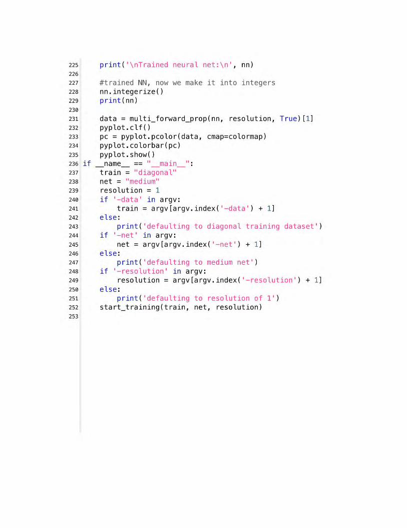
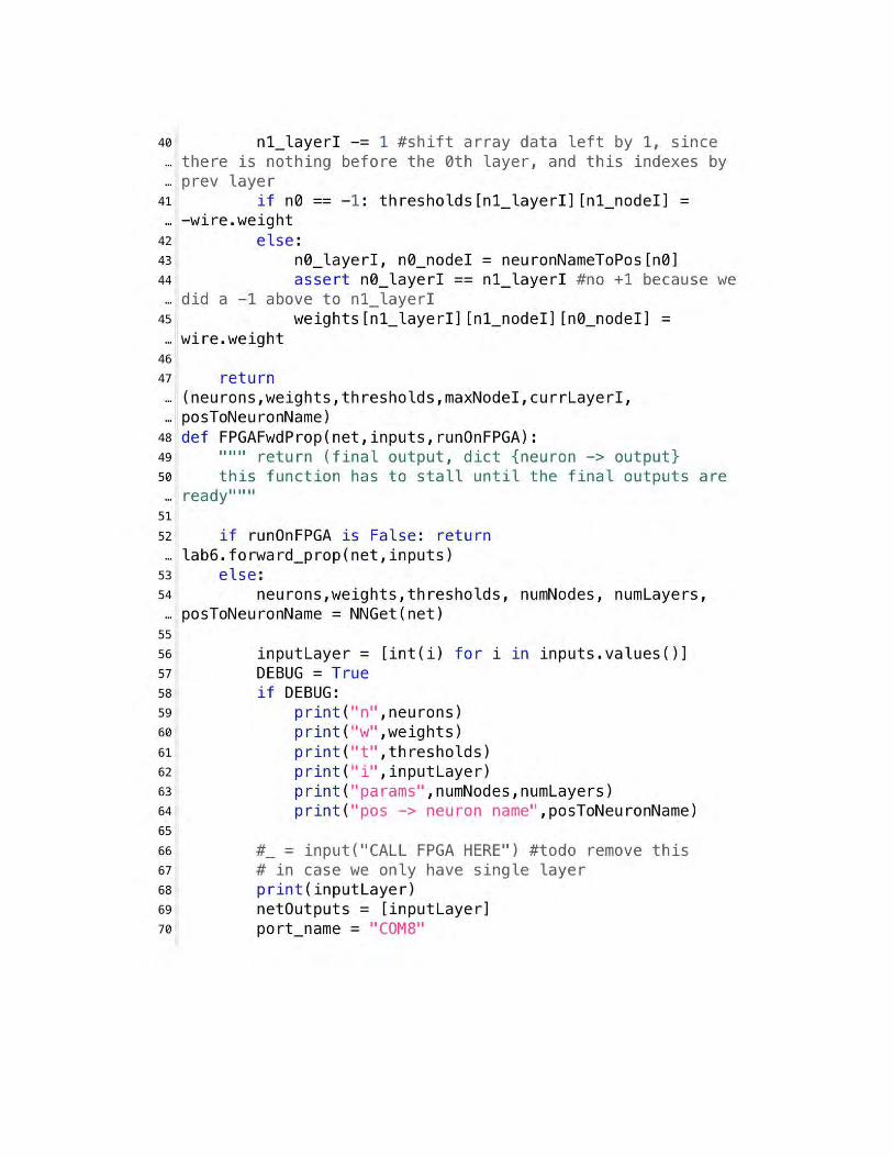
Appendix B: Python Visualization Code (Note: Solutions to the 6.034 lab assignment have been intentionally omitted. These are not key files in interfacing the FPGA neural network with the “training.py” script that is given as part of the 6.034 starting lab material, which has been modified to suit this project.) Main Script (app.py)


Communications (comm.py)


Lab Interface (labinterface.py)


Training (training.py, modified version of 6.034 starting code)