O Marketing Guiado por Dados – Mais conversão e Mais Retorno ao seu Investimento

Satellite Electrical Power System
Nuno Laranjeira Ramos
Thesis to obtain the Master of Science Degree in
Electronics Engineering
Supervisors: Prof. Maria Beatriz Mendes Batalha Vieira Vieira Borges
Prof. Moisés Simões Piedade
Examination Committee
Chairperson: Prof. Pedro Miguel Pinto Ramos
Supervisor: Prof. Maria Beatriz Mendes Batalha Vieira Vieira Borges
Members of the committee: Prof. Marcelino Bicho dos Santos
October 2018

1
Abstract
The Electrical Power System (EPS) is an electronic circuit board that is designed to supply and
manage process the energy in an efficient way. This document describes the design architecture and
circuits involved for an EPS deployed in the ISTsat ONE nano satellite project. The EPS generates
energy through its solar panels which is stored in the battery and then, using DC-DC switching voltage
regulators, converts it to the final voltage of +3.3 V and +5 V, supplying these voltage rails for the rest
of the subsystems of the satellite. This architecture meets the performance and size requirements of
CubeSat architecture (cubic shape with 10 cm of edge, satellite with less than 10 kg). The EPS is
composed by various systems, namely: Maximum Power Point Tracking mechanism to achieve
maximum efficiency in the conversion of solar energy, a 20.8 Wh battery, solar panels and redundant
circuitry to continuously ensure the power supply to the satellite. The EPS is a subsystem of the
ISTsat ONE and as such, it communicates with other subsystems present in the satellite sending data
logs, error warnings as well as receiving commands.
Keywords – EPS, Electrical Power System, Battery, Space, CubeSat, Nano satellite, ISTsat ONE,
Power System, DC/DC Converter, Solar Panel, Energy Management, Maximum Power Point tracker,
Solar Panels
2
Resumo
O sistema de energia elétrica (EPS – Electrical Power Supply) é constituído por uma placa de
circuito eletrónico projetado para fornecer e gerir a energia de forma eficiente. Este documento
descreve a arquitetura e o desenvolvimento dos circuitos eletrónicos envolvidos num sistema de
energia elétrica implementado para o nano satélite ISTsat ONE. O sistema gera energia elétrica através
de painéis solares. A energia é armazenada na bateria que por sua vez alimenta reguladores de tensão
comutados de corrente contínua (DC-DC), convertendo e regulando a tensão final nos valores de +3.3 V
e +5 V, fornecendo alimentação para o resto dos subsistemas do satélite. Esta arquitetura considera
os requisitos de desempenho e as características físicas da arquitetura CubeSat (satélite com menos
de 10 kg, com formato cúbico e 10 cm de aresta). Para garantir a alimentação do satélite, são
implementados vários sistemas: o mecanismo de rastreamento de ponto de potência máxima para
alcançar a máxima eficiência na conversão da energia solar, uma bateria de 20.8 Wh, painéis solares
e circuitos redundantes. O EPS sendo um subsistema do ISTsat ONE comunica com outros
subsistemas presentes no satélite recebendo comandos e enviando registos de dados e avisos de
anomalias.
Palavras chave – 1 U, Sistema de Energia Elétrica, EPS, Espaço, CubeSat, Nano satélite, ISTsat ONE,
Sistema de Gestão de Energia, Conversor DC/DC, Painel Solar, Módulo de Alimentação do satélite.

3
Acknowledgements
Firstly I would like to thank my mentors Professor Maria Beatriz Mendes Batalha Vieira Vieira
Borges and Professor Moisés Simões Piedade for all their support, dedication and knowledge without
whom this work would have not been possible. Their guidance and teachings, both scientifically and life
experience, contributed for me to be a better engineer as well as a better person, I shall embrace them
for life.
I wish to thank Professor Rui Manuel Rodrigues Rocha, for the opportunity to work and be a part
of the ISTsat ONE project as well as his support throughout this dissertation.
In this project I have had the pleasure to work with the ISTsat ONE team, to whom I am grateful
for their support and contribution to this project.
Nobody has been more important to me in the pursuit of my academic goals than my parents. I
am especially grateful to my father Alfredo Ramos and my mother Maria Ramos. Their special love,
care and guidance helped me to achieve all my goals and overcome all challenges in life.
Finally, for the financial support I would like to thank to Instituto de Telecomunicações (IT),
Instituto de Engenharia de Sistemas e Computadores (INESC-ID), Associação Portuguesa de
Amadores de Rádio para Investigação, Educação e Desenvolvimento (AMRAD) and Instituto Superior
Técnico (IST).

4
Table Contents
Abstract ................................................................................................................................................... 1
Resumo .................................................................................................................................................... 2
Acknowledgements ................................................................................................................................. 3
Table Contents ........................................................................................................................................ 4
List of Figures ........................................................................................................................................... 7
List of Tables .......................................................................................................................................... 10
List of Abbreviations .............................................................................................................................. 11
Chapter 1 Introduction ....................................................................................................................... 13
1.1 Motivation ............................................................................................................................. 13
1.2 Project Goals ......................................................................................................................... 14
1.3 System Requirements ........................................................................................................... 14
1.4 Document Layout/Organization ............................................................................................ 16
State of Art ........................................................................................................................ 17
2.1 Nano satellites and CubeSat .................................................................................................. 17
2.2 Commercially available EPS ................................................................................................... 19
2.2.1 Clyde-Space EPS............................................................................................................. 19
2.3 Related EPS Components ...................................................................................................... 21
2.3.1 Solar panels ................................................................................................................... 21
2.3.2 MPPT and Battery Charger Regulator ........................................................................... 22
2.3.2.2 Direct Energy Transfer (DET) with Regulated Bus ......................................................... 23
2.3.2.3 Maximum Power Point Tracker and Battery Charge Regulated Bus ............................. 23
2.3.3 Battery ........................................................................................................................... 24
2.4 ISTSat ONE first EPS prototype .............................................................................................. 25
ISTSat ONE EPS .................................................................................................................. 27
3.1 Solar Panels ........................................................................................................................... 29
3.1.1 Solar Cell Model............................................................................................................. 29
3.1.2 Series Connection of two cells ...................................................................................... 30
3.1.3 Parallel connection of solar cells. .................................................................................. 31
3.1.4 Electrical Connection of Solar panels ............................................................................ 32
3.2 MPPT Converters ................................................................................................................... 32
3.3 Battery Charger ..................................................................................................................... 37
3.4 Battery ................................................................................................................................... 38

5
3.5 Multiplexer Switches ............................................................................................................. 42
3.6 RBF pin & deployment switches ............................................................................................ 42
3.7 Latch Memory circuit ............................................................................................................ 44
3.8 Buck Converters .................................................................................................................... 45
3.9 Power Distribution Module ................................................................................................... 46
3.10 Microcontroller ..................................................................................................................... 47
3.11 EPS Analog Sensors................................................................................................................ 48
3.11.1 Voltage Sensing ............................................................................................................. 49
3.11.2 Current sensors ............................................................................................................. 50
3.11.3 Temperature Sensors .................................................................................................... 52
3.12 Software ................................................................................................................................ 52
3.12.1 Functions Overview ....................................................................................................... 53
3.12.2 Operation modes ........................................................................................................... 55
3.12.3 Interrupt Service Routines ............................................................................................. 56
Energy Budget ................................................................................................................... 58
4.1 Expected Energy Generation ................................................................................................. 58
4.2 ISTSat ONE Power Consumption ........................................................................................... 59
4.3 ISTSat ONE Energy Budget..................................................................................................... 61
Testing platforms ............................................................................................................... 63
5.1 Automated Measurement System ........................................................................................ 63
5.1.1 Battery Tester ................................................................................................................ 64
5.2 FlatSat Board ......................................................................................................................... 66
EPS Prototype .................................................................................................................... 67
6.1 EPS PCB Layout ...................................................................................................................... 67
6.2 Battery Layout ....................................................................................................................... 68
6.3 EPS electrical Specifications & requirements ........................................................................ 69
EPS Performance ............................................................................................................... 71
7.1 Analog Sensors ...................................................................................................................... 71
7.2 MPPT Converter .................................................................................................................... 72
7.3 Battery Charger ..................................................................................................................... 76
7.4 Battery ................................................................................................................................... 78
7.5 Deployment Switches, Remove Before Flight Cut off Circuitry and Initialization Latch circuit
(MUX Module) ................................................................................................................................... 79
7.6 Buck Converters .................................................................................................................... 80
7.7 Power Distribution Module ................................................................................................... 83

6
7.8 EPS Performance ................................................................................................................... 86
Conclusion ......................................................................................................................... 89
Future Work .......................................................................................................................................... 91
References ............................................................................................................................................. 92
Annexes ................................................................................................................................................. 93

7
List of Figures
Figure 1.1 – Example of an ADS-B network with a satellite. ................................................................. 13
Figure 1.2 – Physical layout design of the Clyde Space 3rd generation 1U EPS with integrated battery
(all values presented are in millimetres) [7]. .......................................................................................... 16
Figure 1.3 – PC104 connector and typical pin out connections [21]. .................................................... 16
Figure 2.1 – Nano satellites launched and announced, until December 2017 [5]. ............................... 18
Figure 2.2 – CubeSat classes launched, until December 2017 [5]. ...................................................... 19
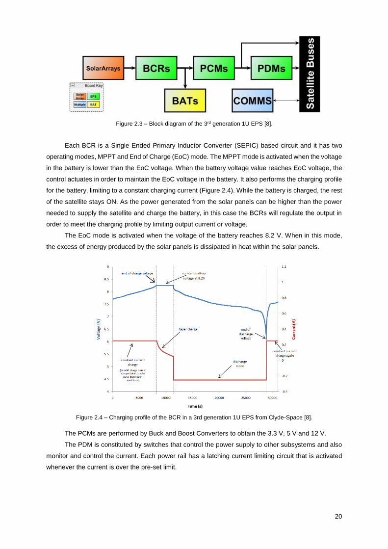
Figure 2.3 – Block diagram of the 3rd generation 1U EPS [8]. .............................................................. 20
Figure 2.4 – Charging profile of the BCR in a 3rd generation 1U EPS from Clyde-Space [8]. ............. 20
Figure 2.5 – Deployable solar panels installed on a CubeSat. ............................................................. 21
Figure 2.6 – Representative layers of a triple junction solar cell [6]. ..................................................... 22
Figure 2.7 – Design architecture of the Direct Energy Transfer [16]. .................................................... 22
Figure 2.8 – Design architecture of the Direct Energy Transfer using a Battery Charge/Discharge
Regulator [16]. ....................................................................................................................................... 23
Figure 2.9 – Design architecture of a Maximum Power Point Tracker and Battery Charge Regulated Bus
[16]. ........................................................................................................................................................ 24
Figure 2.10 – ISTSat ONE first EPS developed prototype [17]............................................................. 25
Figure 2.11 – Blocks diagram of the ISTSat ONE first EPS prototype. ................................................ 25
Figure 3.1 – Block diagram representing the EPS power flow. ............................................................. 27
Figure 3.2 – Detailed functional diagram of the ISTSat ONE EPS. ...................................................... 28
Figure 3.3 – 1U solar panel from Endurosat. ........................................................................................ 29
Figure 3.4 – Solar Cell model. ............................................................................................................... 30
Figure 3.5 – Series connection of two solar cell models. ...................................................................... 30
Figure 3.6 – Parallel connection between solar cells. ........................................................................... 31
Figure 3.7 – Solar panel power output comparison for different Luminance. ...................................... 32
Figure 3.8 – Maximum power point tracking circuit, boost converter .................................................... 33
Figure 3.9 – Inductor voltage and current in a period at the limit of continuous current mode [23]. ..... 33
Figure 3.10 – Characteristic curve (Current vs Voltage) of the solar panel, under AM0 solar radiation
conditions............................................................................................................................................... 35
Figure 3.11 – Incremental Conductance MPPT algorithm. ................................................................... 36
Figure 3.12 – Flowchart for the control of boost converter. ................................................................... 37
Figure 3.13 – Flowchart of the MPPT module mode decision. ............................................................. 37
Figure 3.14 – Circuit diagram of the SEPIC. ......................................................................................... 38
Figure 3.15 – Battery cell (Left top / Right Bottom). .............................................................................. 38
Figure 3.16 – Battery pack circuit diagram. ........................................................................................... 39
Figure 3.17 – Battery heater board (CAD design). ................................................................................ 40
Figure 3.18 – Internal Resistance Measurement Circuit with the DC battery model. ........................... 41
Figure 3.19 – Flowchart of the State of Charge value iteration. ............................................................ 41

8
Figure 3.20 – Multiplexer Schematic Circuit. ......................................................................................... 42
Figure 3.21 – Detailed diagram block of the RBF pull pin actuators. .................................................... 43
Figure 3.22 – Deployment switches 1 and 2 circuitry ............................................................................ 43
Figure 3.23 – Deployment switch 3 circuitry .......................................................................................... 43
Figure 3.24 – Latch memory circuit diagram. ........................................................................................ 44
Figure 3.25 – Circuit diagram of the synchronous buck converter ........................................................ 46
Figure 3.26 – Blocks diagram of the Power Distribution Module. ......................................................... 46
Figure 3.27 – ISTSat ONE I2C architecture blocks diagram. ................................................................ 48
Figure 3.28 – Multiplexing scheme for analog sensors. ........................................................................ 49
Figure 3.29 – Resistive voltage divider circuit. ...................................................................................... 49
Figure 3.30 – Current sensor diagram [20]. .......................................................................................... 50
Figure 3.31 – General current sensing circuit. ...................................................................................... 50
Figure 3.32 – PDM current sensing circuit. ........................................................................................... 51
Figure 3.33 – Battery current sensing circuit. ........................................................................................ 51
Figure 3.34 – Battery temperature sensing circuit. ............................................................................... 52
Figure 3.35 – Battery temperature sensors relation curve (Temperature Vs Output Voltage). ............ 52
Figure 3.36 – "main" function flowchart. ................................................................................................ 54
Figure 3.37 – Operation modes procedures.......................................................................................... 55
Figure 3.38 – Operating mode state chart representing the operation modes of the EPS. .................. 56
Figure 4.1 – Orbit Illustration for ISTSat ONE ....................................................................................... 59
Figure 4.2 – Power generation graph. Without the eclipse of the sun by the Earth, and with 2 pairs of
panels simultaneously light.................................................................................................................... 59
Figure 4.3 – Power generation graph. With the eclipse of the sun by the Earth and with 2 pairs of solar
panels. ................................................................................................................................................... 61
Figure 5.1 – Rack shelf containing the Instruments that Compose the Automated measurement system.
............................................................................................................................................................... 63
Figure 5.2 – Connections diagram of the AMS with a battery cell. ....................................................... 64
Figure 5.3 – Internal Resistance Measurement with current pulses. .................................................... 65
Figure 5.4 – Two FlatSat test boards for ISTSat-ONE Sub-systems interconneted. ............................ 66
Figure 6.1 – EPS prototype PCB (Left – Top View / Right – Bottom View). ......................................... 67
Figure 6.2 – Middle-Bottom layer of the EPS PCB showing the ground planes. .................................. 68
Figure 6.3 – Picture of the ISTSat ONE Battery Pack. (Left - Top view; Right - Bottom view). ............ 68
Figure 6.4 – Battery disassembled displaying on the left the battery heaters and on the right the cells.
............................................................................................................................................................... 69
Figure 7.1 – MPPT converter transient signals considering light radiance in the panels: Continuous
Current Mode (CCM) with an output current load of 173 mA (on the left); boundary between CCM and
Discontinuous Current Mode (DCM) with an output load of 52.5 mA (on the right). ............................. 72
Figure 7.2 – MPPT convergence test. ................................................................................................... 73
Figure 7.3 – Radiation variance test to the converter in MPPT mode. ................................................. 73
Figure 7.4 – Input voltage variance test with the MPPT in Boost mode. .............................................. 74
Figure 7.5 – Transition between the MPPT and BOOST modes. ......................................................... 75

9
Figure 7.6 – MPPT converter power efficiency. .................................................................................... 75
Figure 7.7 – Input Voltage sweep test from 0 V to 15 V. ....................................................................... 76
Figure 7.8 – Battery Chargers Input Power limited by current to 350 mA. ............................................ 76
Figure 7.9 – Battery Charger Output Voltage load sweep test. ............................................................. 77
Figure 7.10 – Battery Charger Power Efficiency results for different input voltages. ............................ 77
Figure 7.11 – Full discharge and charge cycle cell result profile (0.42C @ 28 ºC)............................... 78
Figure 7.12 – ISTSat ONE battery pack discharge and charge profile results (0.33C @ 25ºC). .......... 78
Figure 7.13 – Latch memory discharge profile. ..................................................................................... 80
Figure 7.14 – Buck converter 2 (3.3 V) input voltage sweep with a 15.7 Ω resistor connected to the
output. .................................................................................................................................................... 81
Figure 7.15 – Buck converter 2 (3.3 V) output load sweep test with 7.4 V at the converter input. ....... 81
Figure 7.16 – Buck converter 2 with a transient load applied (10 kHz, duty cycle 15%, High Current 900
mA, Low Current 250 mA). .................................................................................................................... 82
Figure 7.17 – Buck converter 2 (3.3 V) Power Efficiency vs Output Power. ......................................... 82
Figure 7.18 – Efficiency comparison between buck converters 2 and 3 (output 3.3 V) for an input voltage
of 7.4 V. ................................................................................................................................................. 83
Figure 7.19 – OBC subsystem power supply output (VCC1) load sweep test. ..................................... 84
Figure 7.20 – OBC subsystem power supply output (VCC1) shorted to ground. ................................. 84
Figure 7.21 – OBC subsystem power supply output (VCC1) under heavy loads transient .................. 85
Figure 7.22 – DC power supply configuration, I(V) characteristic and power curve. ............................ 86
Figure 7.23 – Overall EPS experiment with the battery mounted, two MPPTs generating power for power
inputs conditions set in Figure 7.22. ...................................................................................................... 87
Figure 7.24 – EPS Overall Efficiency with supply power in (5 V) through X axis MPPT, without the battery
connected and a variable load applied to the OBC subsystem output. ................................................ 88

10
List of Tables
Table 1.1 – Peak Power Consumption of the ISTSat ONE Sub systems and devices. ........................ 15
Table 2.1 – Satellite group names based on mass [10]. ....................................................................... 17
Table 2.2 – Comparison of the characteristics between battery types. ................................................ 25
Table 3.1 – RBF pin and deployment switches truth table. ................................................................... 44
Table 3.2 – Voltage divider resistor and output values. ........................................................................ 49
Table 3.3 – Current sensors characteristics. ......................................................................................... 51
Table 4.1 – S/C Power Figures ............................................................................................................. 60
Table 4.2 – S/C Energy Budget. ............................................................................................................ 62
Table 6.1 – Electrical characteristics of the EPS. ................................................................................. 70
Table 7.1 – EPS voltage measurement associated errors. ................................................................... 71
Table 7.2 – EPS current measurement associated errors. ................................................................... 71
Table 7.3 – EPS temperature measurement associated errors. ........................................................... 71
Table 7.4 – Comparison results for battery heaters (@3.3V)................................................................ 79
Table 7.5 – Power Cut-off switches validation results and power consumption. .................................. 79
Table 7.6 – Electrical characteristics for the buck converters. .............................................................. 83
Table 7.7 – PDM Voltage output measurement results. ....................................................................... 85
Table 7.8 – PDM Maximum Current output measurement results. ....................................................... 86
Table 7.9 – PDM Maximum Power output measurement results. ......................................................... 86

11
List of Abbreviations
1U – One Unit cube sat system
ADC – Analogue to Digital Converter
ADCS – Altitude and Determination Control System
ADSB – Automatic Dependent Surveillance Broadcast
AMS – Automated Measurement System
BCR – Battery Charger Regulator
CCM – Continuous Conduction Mode
DCM – Discontinuous Conduction Mode
DoD – Depth of Discharge
EPS – Electrical Power System
ESA – European Space Agency
FYS – Fly Your Satellite
GPIO – General Purpose Input / Output
I2C – Inter-Integrated Circuit
ISC – Short Circuit Current
ISR – Interrupt Service Routine
IST – Instituto Superior Técnico
LDO – Low Drop Out
LED – Light Emitting Diodes
Li-Ion – Lithium Ion
Li-Po – Lithium Polymer
LPM – Low Power Mode
MCU – Microcontroller Unit
MOSFET – Metal Oxide Semiconductor Field Effect Transistor
MPPT – Maximum Power Point Tracking
NiCd – Nickel-Cadmium
NiH2 – Nickel Hydrogen
NiMH – Nickel Metal Hydride
OBC – On Board Computer
OCV – Open Circuit Voltage
PCB – Printed Circuit Board
PCM – Protection Circuit Module
PDM – Power Distribution Module
P-POD – Poly Picosat Orbital Deployment
PV – Photovoltaic
RBF – Remove Before Flight
S/C – Space Craft

12
SCC – Short Circuit Current
SEPIC – Single Ended Primary Inductor Converter
SNR – Signal to Noise Ratio
SoC – State of Charge
SoH – State of Health
TT&C – Telemetry, Tracking and Command

13
Chapter 1 Introduction
1.1 Motivation
Man has put satellites on orbit to address the ever growing necessity of connecting every part of
the world. The satellites have various purposes such as telecommunication, space exploring, military
purposes and weather forecast, among others.
The motivation to embrace this work directly derives from the challenging idea of develop, design
and build a satellite with the objective of supporting the Automatic Dependent Surveillance Broadcast
system (ADS-B) via satellite. The satellite receives the identification and position broadcasted by
passing airplanes. As soon as the satellite establishes connection with a ground station it relays back
all the airplanes information back to Earth. This solution addresses the issue of the airplanes loosing
contact with the ground stations, and so failing to report their position, leading to missing airplanes [1][2].
Figure 1.1 – Example of an ADS-B network with a satellite.
The ISTsat ONE project is inserted in the Fly Your Satellite Program from European Space
Agency, which whose purpose is to provide the opportunity to university students to develop and launch
a satellite, whilst deploy an ESA mission, involving real world applications.
The ISTsat ONE is divided into various subsystems namely, the Attitude Determination and
Control System (ADCS) which is responsible for determining in real time, position and satellite
framework with the Earth; the Communications sub-system (COM) which is the system responsible for
all digital communications between the satellite and the ground stations; the On Board Computer (OBC)
sub-system processes the data provided by the on-board components and also has the responsibility
to maintain the proper functioning of the satellite; Telemetry Tracking and Command system (TT&C)
gathers all the relevant information of the satellite (position, satellite attitude, systems status, and
more…) and sends the collected data back to the Ground Station; and finally, the EPS. These
subsystems perform full control of the Space-Craft (S/C). In addition a sub-system is deployed to
perform a scientific experiment or a specific mission, called the Payload that carries out the ADSB
mission.

14
There are many risk factors in space that can jeopardize the S/C, namely: space debris can hit
the S/C damaging the PV cells or internal circuitry; solar radiation; electromagnetic waves; and because
there is no service or repair in space for a nano satellite, due to the incapability of fetching the satellite
once deployed, the EPS must assure that power never fails under any circumstances. This feature is
addressed with by the inclusion of redundant circuitry and energy optimized operation modes.
As referred, due to rigorous specifications and redundancy and also to the responsibility to
provide electrical energy to all the satellite subsystems the EPS electric circuit has inevitably, a complex
architecture. Therefore, in order to facilitate the design, the EPS is divided in four sections: The design
chosen to the EPS electric circuit is divided in four sections: the converters used to regulate power
collected by solar panels; the architecture for distribution or storage of the energy collected in the battery,
the power distribution module that converts energy in regulated outputs used for supplying power to all
the S/C, and the section devoted to the microcontroller used to collect measurements and carry out the
monitoring of all the EPS.
1.2 Project Goals
This project is part of the ISTsat ONE satellite project, which is developed by students of IST. All
of the satellite subsystems are developed in house as well as some of its components. The goal is to
develop an EPS to power and manage the energy of the ISTsat ONE. Through the developing process
the hardware is produced and tested as well as the software.
The EPS must be able to harvest energy from the solar panels and store it in the battery, as well
as delivering power to the satellite, using switched controlled converters to supply regulated voltage. As
referred, it must also present redundant circuitry to ensure that in case of failure the power of the satellite
is never down.
The software is implemented in order to manage the overall energy of the satellite, regulate the
converters to extract maximum power from solar panels, perform power diagnostics, engage redundant
circuitry and to communicate with the OBC. In this document the process of developing the EPS is
described, by addressing the hardware design and architecture, its physical characteristics and the
involved software.
1.3 System Requirements
In this section the ISTsat-ONE requirements for the EPS are presented:
The charging starts when the battery temperature is appropriated (between 0 ºC and 40 ºC).
The EPS receives commands via the I2C bus.
The requests for the EPS module information's use the main I2C bus.
The EPS must continue to generate power to the buses if a software crash should occur.
The EPS must have redundant circuitry to generate power to the voltage buses.
The EPS must have five individual power lines to supply the satellites sub-systems.
The EPS must control individually the supply of the power lines.
The EPS must have a dedicated battery charger IC controller.

15
The EPS must generate the 3.3 V, 5 V voltage buses (10% tolerance) and distribute them to
other systems.
Minimum peak power for each bus is 4 W.
Minimum total buses simultaneous peak power is 12 W (see Table 1.1).
The EPS must have a low power consumption microcontroller to generate the control signals
for the system and the communication with the main system of the S/C.
The EPS must perform MPPT algorithm for each solar panel association.
The solar panels are connected directly to the EPS board.
The EPS must have a charging port.
The EPS must feature RBF switches.
The EPS must perform the initialization procedure following the ISTsat ONE plan.
The system performs auto-diagnostics and deploys available redundant circuits.
The EPS automatically resets the system if a software crash should occur.
The EPS manages automatically the power consumption between battery and the power
generated from the solar panels.
The PC104 connector must follow the standard pin out connections.
The EPS must be compatible with the 3rd generation 1 U standalone battery from Clyde Space
(page 16, Figure 1.3).
Table 1.1 – Peak Power Consumption of the ISTsat ONE Sub systems and devices.
Module Peak [mW]
TTC Rx 400
TTC Tx 2000
Beacon Tx 300
OBC 500
COM 1500
Payload 1000
Magnetorquers 775
Battery Heater 400
Total 6875
Another requirement of the EPS is that it must be fully compatible with other EPSs available on
the market, in case a commercial one should be used, to mitigate the risk of this project time deadlines.
The physical dimensions for the ISTsat ONE EPS are represented in Figure 1.2.

16
Figure 1.2 – Physical layout design of the Clyde Space 3rd generation 1U EPS with integrated battery (all values
presented are in millimetres) [7].
Figure 1.3 – PC104 connector and typical pin out connections [21].
1.4 Document Layout/Organization
This document is organized as follows:
Chapter 1 – Introduction of the theme of this project, its motivation and goals.
Chapter 2 – Description of the state of art related to the developing work of this project.
Chapter 3 – EPS architecture design and definition, implementation of hardware and software.
Chapter 4 – Energy generation, Power and Energy Budget.
Chapter 5 – Testing platforms used and developed to assist the EPS tests.
Chapter 6 – Physical hardware description of the outcome layout design (Battery and EPS).
Chapter 7 – EPS tests and performance results.
Chapter 8 – Conclusion.

17
State of Art
The first artificial satellite to be successfully put on orbit was the Sputnik on 4th October 1957. It
was developed in the USSR and its sole purpose was to transmit radio signals back to Earth that could
be received by any amateur radio. The Sputnik proved that artificial satellites could have a big role in
the future of telecommunications.
With the technological advancements throughout the years, the satellites would last longer on
orbit and started to carry actual missions. This led to a growth in deployment of satellites used in a wide
variety of applications, such as weather forecast, telecommunications, military purposes and so on.
The first amateur satellite to be deployed was the OSCAR-1 on 12th December of 1961, and its
launch inspired other radio amateurs and scientists to develop projects to be launched as well. This led
to the foundation of the space industry where more amateur satellites are deployed continuously
contributing for the space technology to advance.
In order to frame the developed work, this Chapter describes the state of the art of nano satellites
in general, followed by the presentation of the diverse existing types of satellite EPSs commercially
available. Focus is put in the various technologies applied in the EPS, such as the batteries, solar panels
and so on. As there are many different technologies involved, another important aspect to focus is the
overall architecture of the EPS, making sure that all technologies work together and complete each
other.
2.1 Nano satellites and CubeSat
The OSCAR-1 success encouraged the development of new projects in the amateur satellite area
that permitted a faster evolution with new ideas and concepts. With the evolution of technology,
electronic components became smaller decreasing the dimensions of the final product.
Table 2.1 – Satellite group names based on mass [10].
Group name Mass (kg)
Large Satellite >1000
Medium Satellite 500 to 1000
Mini Satellite 100 to 500
Micro Satellite 10 to 100
Nano Satellite 1 to 10
Femto Satellite 0.1 to 1
By reducing the size and weight of the satellite the costs of the satellite launching are significantly
reduced. This had a high impact in the satellite industry, leading to a continuous market growth, not only
in professional business, but also at the amateur level. In 1999, California Polytechnic State University
and Stanford University developed the CubeSat specifications to promote and develop the necessary
skills for the design, manufacture and testing of small satellites intended for Low Earth Orbit (LEO)

18
operation that perform a number of scientific research functions and explore new space technologies.
Later in 2003 the first CubeSat was launched [11].
The CubeSats are a U-class space crafts, meaning that the satellite can be composed of various
units bounded together. Each Unit (1 U) is a cube with 10 cm in each edge and 1 litter of volume
(10x10x10 cm3). With this standardization there was no need to specifically design a new launching craft
and many satellites could be deployed at the same time, highly reducing the cost.
The CubeSats opened an inexpensive opportunity for companies to have their own satellites
driving the missions in a cost effective way. Figure 2.1 shows a bars graph presenting the number of
assigned nano satellites through the years, confirming the increasing launches of this type of satellite.
Figure 2.2 shows that the CubeSat configuration is the most used type of nano satellite, which shows a
large acceptance by the industry and market to the CubeSat standardization. This also led to the advent
of new companies with the purpose of developing and selling their hardware for CubeSats, such as
Clyde-Space, EnduroSat, GOMspace. These companies can provide the whole satellite with the
requirements of a specified mission with the architecture of the CubeSats, or they can simply provide
parts of the satellite, like solar panels or structure, or even electrical modules such as COM, PAYLOAD,
TT&C, and EPS.
Figure 2.1 – Nano satellites launched and announced, until October 2018 [5].

19
Figure 2.2 – CubeSat classes launched, until October 2018 [5].
2.2 Commercially available EPS
As aforementioned there are companies that are dedicated to the manufacture of CubeSat
components such as the EPS. The use of a commercial available module decreases the risk in terms
of proper function and safe operation, because the hardware has proven to be effective by having flown
on other missions with success, as opposed to a newly developed module. However, these EPS
modules are not flexible with customized designs, which means that the satellite must be compatible
with the EPS voltage rails, its weight, dimension and battery placement. Another disadvantage is the
high cost, which can vary between 1.000 € and 8.000 € [12] [13].
2.2.1 Clyde-Space EPS
For a 1U CubeSat, Clyde-Space has the 3rd Generation 1 U EPS [8]. Optionally it can be
equipped with a battery pack, specifically designed for this bundle. The main features include:
• 3.3 V, 5 V, and 12 V regulated power buses,
• Unregulated battery bus,
• 10 Latching Current Limit (LCL) power distribution modules,
• Maximum Power-Point Tracking (MPPT) Battery Charge Regulators (BCRs),
• Over-current, over-voltage and under-voltage protection.
As shown in Figure 2.1, this EPS has three Battery Charger Regulators (BCR) with two solar
panels connected to each BCR. The batteries are connected to the BCRs, which in turn are also
connected do the Power Conversion Modules (PCM). The Power Distribution Modules are connected
after the PCMs and supply the satellite power bus. Figure 2.3 presents the block diagram of the 3rd
generation 1U EPS.
20
Figure 2.3 – Block diagram of the 3rd generation 1U EPS [8].
Each BCR is a Single Ended Primary Inductor Converter (SEPIC) based circuit and it has two
operating modes, MPPT and End of Charge (EoC) mode. The MPPT mode is activated when the voltage
in the battery is lower than the EoC voltage. When the battery voltage value reaches EoC voltage, the
control actuates in order to maintain the EoC voltage in the battery. It also performs the charging profile
for the battery, limiting to a constant charging current (Figure 2.4). While the battery is charged, the rest
of the satellite stays ON. As the power generated from the solar panels can be higher than the power
needed to supply the satellite and charge the battery, in this case the BCRs will regulate the output in
order to meet the charging profile by limiting output current or voltage.
The EoC mode is activated when the voltage of the battery reaches 8.2 V. When in this mode,
the excess of energy produced by the solar panels is dissipated in heat within the solar panels.
Figure 2.4 – Charging profile of the BCR in a 3rd generation 1U EPS from Clyde-Space [8].
The PCMs are performed by Buck and Boost Converters to obtain the 3.3 V, 5 V and 12 V.
The PDM is constituted by switches that control the power supply to other subsystems and also
monitor and control the current. Each power rail has a latching current limiting circuit that is activated
whenever the current is over the pre-set limit.

21
2.3 Related EPS Components
The EPS of a nano satellite can be designed with many different architectures, but some
components are common to all designs, such as:
the solar panels to harvest the energy from the Sun;
a battery charger to manage the charging profile of the battery;
voltage regulators, to feed the regulated power bus of the satellite;
the battery where the satellite stores its energy;
Remove Before Flight (RBF) switches and deployment switches, to cut the power while
the satellite is not deployed.
2.3.1 Solar panels
In an autonomous system such as a satellite the power is generated through the solar panels.
Because satellites are in space environment, the radiation from the Sun is higher than the light that is
radiated if the solar panels were to be used on Earth, this is due to the fact that Earth’s atmosphere
reduces the radiation exposure, ultimately reducing the energy production [14].
The solar panels can be mounted on the satellite faces: top, base and sides. Each solar panel
has solar cells and it can have embedded sensors like temperature sensor, gyroscope and light sensor.
Another feature usually embedded in solar panels is the remove before flight switch pins, and the
magnetorquers which control the satellite’s attitude towards the Earth. One way of increasing the
number of solar cells is to have deployable solar panels as seen in Figure 2.5, this increases the area
that is radiated by the Sun.
Figure 2.5 – Deployable solar panels installed on a CubeSat.
2.3.1.1 Triple Junction Solar cells
For nano satellites high efficiency triple junction cells are used. Each junction is made of different
semiconductors and its junction will be sensible to a different band of wavelengths of the light (Figure
2.6). This increases the efficiency of the cell that can rise up to 29.5%.
The gallium arsenide (GaAs) is the best material known to convert energy of light into electrical
power and this conversion efficiency is about 40% larger than silicon. There are single cell solar panels

22
using GaAs presenting 24 % of energy conversion efficiency. Production of GaAs is about 1000 times
more expensive than silicon. For space applications this is not a big problem and the solar panels
typically have two more semiconductor junctions: one based on Gallium Indium Phosphor (GaIP)
sensible to ultra violet and blue radiation and other based on germanium junction very sensible to
infrared light. This combination raises the solar harvesting energy efficiency.
Figure 2.6 – Representative layers of a triple junction solar cell [6].
2.3.2 MPPT and Battery Charger Regulator
Whenever a solar panel is used, a MPPT converter should be applied in order to extract the
maximum power available. Furthermore, the battery also needs a charger to regulate its current and
voltage while charging. There are various architecture designs that can perform both referred features,
but for specific applications as the ISTsat ONE some are more suitable than others.
2.3.2.1 Direct Energy Transfer (DET)
The simplest design for performing both MPPT and battery charger is the Direct Energy Transfer
[16] method, which transfers the energy directly into the battery bus (Figure 2.7). It uses the Sequential
Switching Shunt Regulator (S3R), to regulate the battery bus.
Figure 2.7 – Design architecture of the Direct Energy Transfer [16].
This design is simple and reliable due to the low number of components used, but it has low
efficiency as it does not perform the MPPT. Therefore, the only way to regulate the battery voltage is to

23
cut the power from the solar panels by shorting the solar panels terminals. This also inhibits the energy
going to the PDM. The energy available in the solar panels will be dissipated on the electronic power
switches.
2.3.2.2 Direct Energy Transfer (DET) with Regulated Bus
One way to improve the DET architecture is by using a battery Charge and Discharge Regulator
(Figure 2.8). The battery regulator is independent from the regulated bus, so whenever the battery is
totally charged the power from the solar panels is no longer cut off and the PDM continues to receive
the power available in the solar panels.
Figure 2.8 – Design architecture of the Direct Energy Transfer using a Battery Charge/Discharge Regulator [16].
This solution is more efficient as the power from the solar panels is continuously used, but it still
does not solve the problem of extracting the maximum power from the solar panels.
2.3.2.3 Maximum Power Point Tracker and Battery Charge Regulated Bus
The use of a MPPT converter connected to the solar panels increases the efficiency as the
maximum power is transferred from the radiated energy that is on the solar panels. As each solar panel
has different temperatures and incident radiance angles, the Maximum Power Point (MPP) is also
different. So each solar panel has a MPPT converter to assure that the maximum power available at the
solar panels is transferred independently from their working power points.
The Battery Bus is regulated using the MPPT converters, as shown in Figure 2.9. So the MPPT
also acts as a Battery Charger Regulator. Because the battery requires a charging profile, the
MPPT/BCR operates in two modes, normal MPPT operation and EoC. While the battery is not charged
the converters act as MPPTs, distributing the power to the PDM and charging the battery. Once the
battery is charged the converters are switched in order to regulate to the EoC voltage. At this point the
little energy flows into the battery and the rest will flow directly to the PDM. If the Battery is fully charge
the BCR will maintain the EoC mode and the current will only flow to the PDM.
This architecture has the advantage of having one converter between the solar panel and the
battery bus and it does not require an additional converter to charge the battery nor regulate the Bus
whilst performing the MPP of the solar panels, thus increasing the efficiency. The disadvantage is that

24
it increases the complexity of the design, requiring the use of a micro controller, to drive and control the
operating modes of the BCR/MPPT converters.
Figure 2.9 – Design architecture of a Maximum Power Point Tracker and Battery Charge Regulated Bus [16].
2.3.3 Battery
The battery is one of the most important components in a satellite, as it is where the energy is
stored and what guarantees the continuous functioning of the satellite during the eclipse zone when the
solar panels are not generating any energy.
There are several parameters that must be taken into account when choosing a battery. On a
satellite there are physical limitations regarding its weight and size. In case of a CubeSat the battery
shall not have an area higher than 10 cm x10 cm nor the weight shall be above 10 kg. Apart from
physical parameters, the electrical characteristics of the battery must also be considered: nominal
voltage, discharge and charge currents, number of charging cycles, and its capacity.
Batteries have suffered a lot of evolving across the years by using new materials and by changing
their format and the aforementioned characteristics. The most popular types of batteries use the
following materials: Nickel Cadmium (NiCd), Nickel Metal Hydride (NiMH), Nickel Hydrogen (NiH2),
Lithium Ion (Li-Ion) and Lithium Polymer (Li-Po) [18] [19].
The batteries of NiCd present the advantage of having a linear discharge, great tolerance to
overcharging and lower price when compared to other popular types of battery, but these also have low
energy density (40 Wh / kg). The batteries made of NiMH have a higher energy density (60 Wh / kg)
and also a greater number of charging cycles than NiCd but are more expensive as well. The Li-Po and
Li-Ion became the standard use in space technology due to their high energy density (180 Wh / kg on
Li-Po and 120 Wh / kg on Li-Ion) also due to the number of charging cycles being as high as the NiMH,
whilst presenting higher operating temperatures. The worse disadvantage of the Li-Po and Li-Ion
batteries is the low tolerance to over-charging and over-discharging, which may result in permanent
damage of the batteries [19].

25
Table 2.2 – Comparison of the characteristics between battery types.
Battery Type Energy Density
(Wh/Kg) Operating
temperature [oC] Charging Cycles Nominal Voltage [V]
NiCd 40 -20 – 40 2000 1.2
NiMH 60 0 – 20 30000 1.2
NiH2 65 0 – 20 30000 1.2
Li-Ion 120 0 – 40 30000 3.2 – 3.6
Li-Po 180 0 – 40 30000 3.7
2.4 ISTsat ONE first EPS prototype
The presented project is based on the first EPS prototype (Figure 2.10) that was developed for
the ISTsat ONE. At that time it accomplished the power supply requirements of the ISTsat ONE.
Figure 2.10 – ISTsat ONE first EPS developed prototype [17].
This EPS features connection of five solar panels with three MPPT converters, and includes a
battery charger, a boost converter to achieve 12 V, two Single Ended Primary Inductor Converters
(SEPIC) to achieve 5 V and 3.3 V. This EPS also features redundancy for the final regulation. The
implementation for this redundancy is by step-down the voltage supplied from higher voltage buses, as
shown in Figure 2.11.
Solar Panel+X
Solar Panel-X
Solar Panel+Y
Solar Panel-X
Solar PanelZ
MPPT
MPPT
MPPT
Battery Charger Battery
Boost 12 V
Buck 5 V
Buck 3.3V
Linear Voltage Regulator
SEPIC 5 V
SEPIC 3.3 V
Linear Voltage Regulator
Linear Voltage Regulator
PC104BUS
Microcontroller
Figure 2.11 – Block’s diagram of the ISTsat ONE first EPS prototype.
The MPPT and SEPIC converters pulses are controlled by the microcontroller. The boost and the
bucks have a dedicated Integrated Circuit (IC) that controls and drives the circuits. The linear voltage

26
regulator offers more redundancy in terms of regulation, if all other converters fail. The battery charger
is a linear circuit and also features its own IC controller.
This EPS is functional, however the ISTsat ONE electrical and design specifications have
changed since then and therefore this new project aims to meet the new requirements which are
presented in section 1.3. For instance this version of the EPS does not feature individual supply to each
of the sub-systems, the microcontroller does not have a dedicated power supply, nor does the battery
feature heaters. There are other new requirements which this EPS does not meet. This new project also
focus in improving this architecture efficiency by using switched power converters, and minimizing the
number of conversion stages to achieve final regulation while maintaining and redundancy features.
One of the aspects that can be improved the fact that the MPPT is able to charge directly the battery,
because it does not employ bidirectional switches nor does the MPPT converter perform the charging
profile or regulates the output voltage.
In terms of satellite functionality it is necessary that the new EPS features a Remove Before Flight
Cut power cut off pin, and deployment switches. The new EPS must also feature I2C communication
with other sub-systems.

27
ISTsat ONE EPS
This chapter describes in detail the EPS in general, referring its main components and functions
and also the system’s requirements in order to present to the reader a complete overview of the EPS
developed in this work.
The ISTsat ONE electrical power subsystem uses five triple junction solar panels, a battery with
two lithium cells in series, an in-house designed controller and a supervisor system. A charging port will
be available to recharge the battery while the satellite is grounded. The blocks diagram in Figure 3.1
represent the different stages of energy processing and indicate the power flow of the EPS architecture.
Solar Panel+X
Solar Panel-X
Solar Panel+Y
Solar Panel-X
Solar PanelZ
MPPT
MPPT
MPPT
Battery Charger
Battery
Buck 5 V
Buck 3.3 V
Buck 3.3 V
PC104BUS
MicrocontrollerCharging Port Buck 3.3 V
Permanent regulated 5 V
Permanent regulated 3.3 V
TTC Power
OBC Power
PAYLOAD Power
COM Power
Solar Panels Power
Battery Power
I2C
Figure 3.1 – Block diagram representing the EPS power flow.
As shown in Figure 3.1 there are five solar panels and only three MPPT converters. The solar
panels are mounted on each face of the satellite associated with the respective axis (X,Y,Z). The solar
panels are arranged in opposite faces of the cube (-X / +X, -Y / +Y axis and one panel is mounted on
+Z, -Z face is reserved to accommodate the Payload subsystem antenna). With this arrangement the
MPP of each individual solar panel can be tracked, mind that when +X is illuminated, the -X is in the
dark side. The panel that is in the dark is not producing energy, and so the tracking is made only by the
panel that is light.
The system voltage regulation is achieved in a two-stage process. In the first power processing
stage, the input voltage coming from the solar panels is converted to an intermediate voltage using a
MPPT. At this point the voltage will vary between 4 V and 15 V depending on the energy produced by
the solar panels. The second stage involves the output voltage regulators and current limiting systems
that will feed all the satellite subsystems.
A dedicated microprocessor is responsible for the EPS management. It controls and monitors key
currents and voltages points within the EPS, handles communication with the OBC, controls the power
lines that supply other sub-systems and if necessary engages redundant circuitry. The microcontroller

28
also implements the MPPT algorithm controlling the MPPT switching. This system is able to furnish all
details of the available voltages, current consumption, available energy on the batteries and on the solar
panels, and State of Charge (SoC).
This design also takes into consideration redundancy circuitry so that, in case a component
should fail, the power at PC104 connector is guaranteed at all times, although decreasing efficiency.
The above proposed architecture allows for the energy that is coming directly flowing from the solar
panels to be fed directly to the output voltage regulators through the power multiplexer, without involving
the battery.
A SEPIC converter was selected as a battery charger considering its ability to both step up and
down the voltage, which is necessary due to the MPPT profile. It also performs the charging profile
required to charge the battery. The charger also accomplishes the charging while the satellite is not
launched through a service port.
As referred, for redundancy purposes, the final 3.3 V regulator is repeated so that in case one
should fail, the other should provide the power. In normal operation the power load between the final
regulators is evenly distributed so that any voltage drops or signal noise caused the sub systems be
reduced. The EPS architecture will work with solar panels (without battery). If the microprocessor fails
the solar panels output power will be available to generate the output regulated voltage of 3.3 V. Figure
3.2 represents the detailed EPS block diagram with redundancy circuit and micro controller signals.
Figure 3.2 – Detailed functional diagram of the ISTsat ONE EPS.
The EPS also features a latch memory circuit that stores the initialization state of the satellite.
This serves the purpose of the satellite being resettable with the RBF pull pin, and at the same time hold

29
the initialization state if the system power fails. The latch is set after the initialization procedure is
complete.
Regarding commercial standards, and compatibility purposes, the PC104 connector (Figure 1.3)
pin out and its functions were mapped in accordance.
As previously shown the EPS architecture consists on the integration of modules such as the
MPPT converters, the Battery Charger, Power Distribution Module and others. The explanation of each
module function is presented by resourcing to the EPS blocks’ diagram depicted in Figure 3.2. To
facilitate and better comprehend the implications between modules, the following sections describe each
one of these modules following the power flow, starting with the energy source (solar panels and battery)
and finishing at the final bus power lines (Power Distribution Module).
3.1 Solar Panels
The solar panels are one of the most vital components of the whole satellite, as it is the only
source of energy. As such, the satellite has specific energy requirements which are presented in section
1.3 and must be taken under consideration. When designing the architecture, aspects related with the
selection of solar panels as the definition of panels quantity and their disposition (series or parallel) may
have a great effect on the overall efficiency of the designed system.
All of the solar panels used are triple junction solar cells (see section 2.3.1.1) with two cells
connected in series. The solar panels are from EnduroSat. These commercial panels were chosen as
they fulfil the requirements of ISTsat ONE (Figure 3.3). The solar panel generates 4.66 V of Open Circuit
Voltage (OCV), 0.517 A of Short Circuit Current (SCC) and a maximum power output is 2.4 W. These
figures concerning the electrical characteristics are only valid for the Beginning of Life of the solar panel.
Figure 3.3 – 1U solar panel from Endurosat.
3.1.1 Solar Cell Model
A simple model of a solar cell (or photodiode) (Figure 3.4) may be composed by a DC current
generator with the Short Circuit Current (SCC or ISC) value, biasing an ideal semiconductor junction. The
Model can be completed with the series resistance of the bulk semiconductor accessing to the junction
and the resistance of conductor stripes, RS, a leakage resistance, Rlk and a capacitance that includes a
diffusion capacitance of the junction CD and the capacitance of the spatial charge region CJ.

30
CJCDRlk
RL
iD
uD uO
iORS
ISC
Figure 3.4 – Solar Cell model.
Considering the model in Figure 3.3, when the output current iO is time switched, as is the case
of this architecture, where an MPPT converter is employed, it must be taken into consideration the effect
of using high CD values. Usually, for DC applications it is considered that CD = CJ = 0 and Rlk = ∞[29].
The maximum power available from the solar cell can be obtained by derivation of the output
power (PO) relatively to a resistive load RL. However this equation is very complex, but fortunately can
be approximated by a practical design rule (1) that gives the optimum value of RL[29].
𝑅𝐿 = 0.9𝑉𝑂𝐶
𝐼𝑆𝐶
(1)
This value can be obtained by measuring the open circuit voltage and the short circuit current
(iSC) of the cell.
3.1.2 Series Connection of two cells
In order to obtain higher voltages solar panels are constituted by association of solar cells in
series. The panel can be characterized by its short circuit current and open circuit voltage. In series
connection of cells, the maximum current available of the panel is the smallest current generated in any
cell. When there is a shade over a cell, the current generated may be zero and all other cells generate
current and have higher voltage at their terminals than the shaded one. This makes the biasing of the
shaded cell inversely polarized by the voltage of all the others cells and the load. Solar cells are made
with very thin semiconductor junctions and as a consequence they have a very low maximum reverse
voltage (before junction damage). This is the reason why all cells in large solar panels have a reverse
diode (D3 and D4 in the Figure 3.5) connected in parallel with the cell to limit the reverse voltage to its
forward voltage.
RL
iD1
uD1
uO
iO
iD2
uD2
D3
D4
ISC1
ISC2
Figure 3.5 – Series connection of two solar cell models.

31
3.1.3 Parallel connection of solar cells.
In order to obtain higher currents larger cells can be used. Although this approach is more
expensive rather than using smaller cells in parallel. So this type of connection between cells is common
to use.
As an example, two cells with same solar generated current, connected in parallel, deliver the
same output voltage to the load with the double of the current. In this case there are no issues with
shades over one of the cells.
RL
iD1
uD1
iO1
iD2
uD2
RS1
RS2
uO
iO2
iO
ISC2
ISC1
Figure 3.6 – Parallel connection between solar cells.
An extreme example is the case concerning one cell exposed and the other not exposed to solar
radiation. In this case ISC1 = 1 A and ISC2 = 0 A. This case is common in nano-satellites solar panels
where panels in opposite faces of the cube are connected in parallel. The total current generated is
ISC1 + ISC2 = 1 A and the current on each cell is 0.5 A. The voltage generated in the parallel association
of the cells is lower than the voltage developed in one cell, because now the diode parallel equivalent
has a saturation current that is the double of the saturation current of each cell.
𝑢𝐷 = 𝜂𝑉𝑇 ln (𝑖𝐷
2𝐼𝑠) = 𝜂𝑉𝑇 ln (
𝑖𝐷
2𝐼𝑠) + 𝜂𝑉𝑇 ln (
1
2) (2)
As aforementioned the solar panels consists of two cells in series. Combining the characteristics
of OCV and ISC with (2) [29] it is possible to estimate IS for a temperature of 25 ºC. With that, replacing
the ID with values from 0 A to SCC, the characteristic curve points are calculated and hence possible to
trace the characteristic graph of the solar panel ( Figure 3.7). The output power of the solar cells mostly
varies with the current source present in the solar cell model. The output current reaches its peak when
the radiation is perpendicular to the solar panel (α = 0º, cos(α) = 1), and minimum when the solar panel
parallel to the radiation (α = 90º, cos(α) = 0). With this in mind it is possible to establish the relation
between the solar panel output power versus the incident radiation angle on the solar panel, simply by
multiplying ISC with the cos(α). Figure 3.7 display the comparison for different radiation angles for the
power and I(V) characteristic curves.

32
Figure 3.7 – Solar panel power output comparison for different Luminance.
3.1.4 Electrical Connection of Solar panels
The solar panels are interconnected in different ways forming arrays and this influences the
maximum obtainable power of the array. The best way to obtain the maximum power is by connecting
the panels in parallel. The equivalent panel may introduce a small power loss. That loss depends on the
ratio of the currents generated in each panel. For two equal panels uniformly illuminated and connected
in parallel there is not any loss power loss, i.e., the obtained maximum power is the double of the power
obtained by each isolated panel.
In CubeSats it is typical to connect in parallel the two panels located in opposite faces. In this
case the current generated in the illuminated panel is divided with the other one and there is a small
drop in the OCV of the association. Leading to a small decrease in the power.
Nevertheless, the parallel connection of solar panels presents a problem due to the fact that if
one panel shorts, the power generated by the array is null. To avoid this, usually one diode is associated
in series with each panel and these associations are then connected in parallel, thus furnishing power
to a MPPT circuit. This way if the panel shorts it will be isolated from the array by the associated diode.
However, diodes introduce losses due to their characteristics. MPPT circuits presents better efficiency
when operating with higher power, so it is better to aggregate power with the parallel connection of
panels and minimize the number of MPPT circuits, however this decision will compromise the reliability
of system if one MPPT circuit fails.
3.2 MPPT Converters
To ensure that the maximum power is extracted, a MPPT converter is placed immediately after
the solar panels. As prior referred, this architecture employs three MPPTs, and these are arranged with
two opposing solar panels (+X, -X) per MPPT connected in parallel, except the +Z panel that is
connected singularly to the MPPT due to the –Z face being accommodating an antenna.
The circuit of the MPPT is based on a boost converter as shown in Figure 3.8, and it emulates a
specific load on the solar panels affecting its conductance, forcing the panels to work at maximum
efficiency. This converter is controlled by the micro-controller, meaning that the algorithm is performed
within the micro-controller as well as the measurements and the gate PWM signal.
0
0,5
1,0
1,5
2,0
2,5
3,0
0
0,1
0,2
0,3
0,4
0,5
0,6
0 1 2 3 4 5 6
Po
wer
[W]
Cu
rren
t [A
]
Voltage [V]
Current vs Voltage (α = 0º) Current vs Voltage (α = 45º)
Power vs Voltage (α = 0º) Power vs Voltage (α = 45º)

33
Vsolar panels Vout
Microcontroller
VIN
VL
Figure 3.8 – Maximum power point tracking circuit, boost converter
The boost converter works by controlling the gate of the MOSFET pulses. The MOSFET is N
channel type meaning that when the gate logic level is high (above 1.8 V, due to the threshold voltage
of the MOSFET), it starts conducting and charges the inductor. When the logic level at the gate is low,
the inductor discharges the energy gathered to the output. By switching continuously between these
logic levels it is possible to establish a signal with a defined frequency and duty cycle.
When designing this circuit it was taken into account the switching frequency, and the MPP of the
solar panels. The choosing of the frequency is limited mostly by the micro controller, as the switching
frequency generated by the micro controller affects the PWM settings, limiting the number of steps
between the range of 0% and 100%. The more PWM steps are set the better is the tuning of the
converter and the MPP adjustment. On other way, as the PWM number of steps increases the frequency
decreases. When it comes to switching converters there are some advantages in working at higher
frequencies, such as the decrease of the time response to a perturbation, the reduction of the values of
the components, so is the physical space required for the components, and ultimately for smaller
components the price is also reduced. It was established a compromise between PWM steps and
frequency. The converter switching frequency is 201 kHz, allowing for the micro controller to have 78
PWM steps, which gives approximately 1.282% for each PWM step.
Switching converters are strongly non-linear circuits, however they are linear by steps. Analyzing
the circuit in Figure 3.8, and considering the time intervals during which the MOSFET is ON and OFF,
it is possible to obtain the relation between the average input and output voltages. Figure 3.9 presents
the inductor voltage and current time diagrams for one steady state period when the circuit is operating
at the border of the CCM/DCM.
Figure 3.9 – Inductor voltage and current for one steady state period at the limit of CCM [23].

34
The diagrams in Figure 3.9, are valid only for the continuous conduction mode at the border, as
the current inductor has an average value equal to half of its peak value, ILP . The DCM is characterize
by the existence of null inductor current time intervals within one operating period. If the output current
(equal to the average inductor current) decreases under one half of ILP, circuit enters the DCM.
Considering the voltage time balance at steady state, the mean value of the inductor must be null,
therefore
𝐿 = 0 (3)
When the MOSFET is ON the voltage in the inductor is
𝑇𝑂𝑁 → 𝑉𝐿 = 𝑉𝐼𝑁 . (4)
When it is OFF the voltage becomes
𝑇𝑂𝐹𝐹 → 𝑉𝐿 = 𝑉𝐼𝑁 − 𝑉𝑂𝑈𝑇. (5)
And the mean inductor voltage is given by
𝐿 =1
𝑇∫ 𝑉𝐿 𝑑𝑡
𝐷𝑇
0+
1
𝑇∫ 𝑉𝐿 𝑑𝑡
𝑇
𝐷𝑇. (6)
Combining the equations (3), (4), (5) and (6), the steady state voltage conversion ratio (7) is obtained
(relation between the output and input average voltages versus the duty cycle),
𝑉𝑂𝑈𝑇
𝑉𝐼𝑁=
1
1−𝐷 . (7)
Assuming that the converter has a 100% of efficiency the relation expression for the average values of
the output and currents input is
𝐼𝑂𝑈𝑇
𝐼𝐼𝑁= 1 − 𝐷 . (8)
Analyzing (7), the output voltage can rise above 30 V (e.g. VIN = 3.5 V, D = 90%), surpassing the limits
of the converters and other components that are connected to its output. In order to protect the circuitry
connected to the MPPT output from overvoltage, a Zener diode with a rate of 15 V is connected to the
output of the MPPT.
As stated the value of the MPPT converter components depends on the frequency and on the
MPP of the solar panel. As seen in the previous section the current varies between 0 and 517 mA, and
the voltage can reach up to 4.66 V. So the inductance value must be so that the converter is able to
cope with this magnitude of current. The value of the inductor is obtained through the current expression
flowing in the inductor at the limit of the continuous current mode,
𝐼𝐿𝐵 =1
𝑇∫ 𝐼𝐿𝑑𝑡 =
𝐼𝐿𝑃
2
𝑇
0, (9)
where ILB is the average value of the inductor current which equalizes half of the value of the inductor’s
peak current ILP (calculated at the border of CCM/DCM) (see Figure 3.9) which is obtained by,
𝐼𝐿𝑃 =𝑡𝑂𝑁
2𝐿(𝑉𝐼𝑁). (10)
Combining (7), (8) and (9) the inductance expression is given by
𝐿 =𝑉𝑜𝑢𝑡𝑇
2𝐼𝐼𝑁𝐷(1 − 𝐷). (11)
The MPP of the solar panels is at 4.66 V and 517 mA, so IIN = 517 mA in (11). It is intended that
the output voltage be just over the battery voltage so VOUT = 8.3 V. the duty cycle varies according the
solar panel MPP and the output load. In order for MPPT to have maximum excursion, in (11) D is set to
50%. Finally with T = 5 µs (Frequency of 201 kHz), the calculated inductance is 9.98 µH, which is then
rounded to 10 µH as this is the value that is commercially available.

35
For the capacitors, the higher the capacitance at the input the better. When charging the inductor,
this takes a great amount of current, and the solar panel cannot cope with the necessary current to
charge the inductor. So while the MOSFET is OFF the energy harvested from the solar panels goes to
the capacitors, and when the MOSFET is ON the capacitors along with solar panels provide the energy.
The input capacitance is 22 µF. The output capacitance should be high enough to guarantee low voltage
ripple (less than 10 mV). The minimum capacitance can be calculated through
𝐶𝑚𝑖𝑛 =2𝑃𝑂𝑈𝑇 (1−𝐷)𝑇
(𝑉𝑂𝑈𝑇+𝑉max 𝑟𝑖𝑝𝑝𝑙𝑒)2 . (12)
The minimum capacitance obtained for a ripple of less than 10 mV is 156 nF with D = 10% and with a
output power of 1.2 W. But in order to be able to cope with sudden high current demands, the chosen
capacitance is 100 µF. The electrical schematic of this converter is available in the annex section A3.
The algorithm used is based on the Incremental Conductance MPPT. Because this curve has
only one maximum point, in every perturbation it is possible to find the evolution of the curve and thus
perform the MPPT according to the algorithm described below.
Figure 3.10 – Characteristic curve (Current vs Voltage) of the solar panel, under AM01 solar radiation conditions.
Figure 3.10 presents the I(V) characteristic curve of the solar panel and as shown, the maximum
power is achieved only for a specific current and voltage point. Analyzing the power diagram, it can be
verified when the power reaches its maximum value (13) .
𝑑𝑃
𝑑𝑉= 0 . (13)
The power is given in function of current and voltage by
𝑃 = 𝑉𝐼, (14)
combining (13) with (14) it is obtained (15)
𝑑𝐼
𝑑𝑉+
𝐼
𝑉= 0 ↔
𝑑𝐼
𝑑𝑉= −
𝐼
𝑉 . (15)
Finally the condition for which the maximum power is achieved is verified if (15) is valid. As the software
is not able to compute derivative, it is necessary to make an approximation as
𝑑𝐼
𝑑𝑉≅ 𝐼(𝑉2) − 𝐼(𝑉1). (16)
The algorithm is presented in the flowchart in Figure 3.11.
1 Sun light in space (at top of atmosphere – Air Mass 0, AM0) is equivalent to the radiation of a black body at the temperature
of 5770 K. The light spectrum that reaches earth is called AM1 – Air Mass 1 (1 atmosphere) and is attenuated by the atmosphere.
0,0
0,5
1,0
1,5
2,0
2,5
3,0
0
0,1
0,2
0,3
0,4
0,5
0,6
0 1 2 3 4 5 6
Po
we
r [W
]
Cu
rre
nt
[A]
Voltage [V]
Current (Voltage) Power (Voltage) Maximum Power

36
Adjust PWM Adjust PWM Adjust PWM Adjust PWM
Begin
Yes
No
No
No No
Yes
Yes
No
Yes
Yes
Measure:
Measure:
Figure 3.11 – Incremental Conductance MPPT algorithm.
For the first iteration, an initial duty cycle is set with previous measurements of the solar panels.
Then both current and voltage of the solar panels are measured and a new duty cycle is set accordingly,
and thus the cycle repeats itself.
By adjusting the duty cycle a specific conductance is imposed on the solar panel but in
consequence the output voltage of the MPPT will also vary. As this MPPT is implemented with a boost
converter, increasing the duty cycle at the gate of the MOSFET will result in a higher output voltage
(assuring that the current slope is high enough).

37
Although the main purpose of this circuit is to increase efficiency of the energy harvesting, it can
also operate as a voltage regulator, in this case a step up DC-DC converter or Boost converter. This
feature is crucial as these converters can be directly connected to the battery, bypassing the battery
charger, as previously shown in Figure 3.2. From (7) is possible to extract the procedure for controlling
the boost converter. Whenever the output voltage is below the desired voltage, the duty cycle must be
increased, in turn if the output voltage is above, then the duty cycle is decreased. The output voltage is
set to the battery’s charging voltage of 8.2 V.
Yes
VOUT = 8.2V VBAT < 8.2V
Increase Duty Cycle
Begin
No YesMeasure MPPT VOUT
Increase Duty Cycle
No
Figure 3.12 – Flowchart for the boost converter control.
When charging the battery, the voltage must not exceed 8.2 V and the charging current must also
be limited to 1.2 A, although as shown before in section 3.1, the current will not reach this high because
the power generated by all solar panels is limited. The charging of the battery through the MPPT
converter should be selected as the primary system for charging, once there is only one converter
involved. In fact, charging the battery through the battery charger imposes the existence of two
converters with efficiencies lower than 100%, resulting in power losses increase.
The flowchart in Figure 3.13 presents the decisions and control of the MPPT converter described
above.
No
Yes
VBAT < 8.10V VBAT ≥ 8.2V
Boostmode
Begin No
YesYes
No
MPPTmode
VSOLAR < 0.8 V
MPPTOFF
Figure 3.13 – Flowchart of the MPPT decision mode module.
In case of MPPT failure, the battery charger converter takes over the battery charging ensuring
the charging profile.
3.3 Battery Charger
The battery charger circuit is a SEPIC based (Figure 22). This type of charger was chosen due
to its ability of both step up and down the voltage without changing the positive polarity of the output
voltage. The battery voltage varies between 6.2 V and 8.25 V (discharged and charged respectively),

38
and the output of the MPPT will vary between 4 V and 12 V depending on the load applied to the EPS
and the MPP of the solar panels.
LT1513
Logic Control
VOUTVIN
MCUenable
Figure 3.14 – Circuit diagram of the SEPIC.
This circuit is controlled by the LT1513 IC controller. It has the advantage of being able to setup
the charging current (700 mA) and charging voltage (8.25 V) in order to follow the charging profile of the
battery. It also has the advantage of being monolithic, ensuring compactness. Another feature is the
enable/disable control pin that allows for the micro controller to enable or disable the charging operation.
This charger admits not only input voltage from the solar panels, but it can also receive energy from the
charging port.
This circuit is implemented according to the application note available on the ICs datasheet [28].
The chosen components values chosen also followed the application notes described in the document
[28]. A full schematic is available in the annex A4.
3.4 Battery
The battery is composed by four Varta LPP5037598HH Lithium Ion cells (Figure 3.15). Each cell
has 5.2 Wh of energy capacity, nominal voltage of 3.7 V and the maximum discharge current is 2 A.
These cells come with an embedded NTC temperature sensor and Protection Circuit Module (PCM) for
protection against over discharge (below 3 V), over charge (over 4.32 V) and over current (over 2 A).
Figure 3.15 – Battery cell (Left top / Right Bottom).
The batteries configuration is a two series and two parallel cell connection (2S2P) (see Figure
3.16) which has a total of 20.8 Wh and generates 7.4 V nominal voltage. This arrangement has some
advantages: it allows extracting higher current; but more important it divides the current through the
parallel of each pair of battery series. This way the cells charge and discharge rate is reduced helping
to maintain the battery state of Health (SoH). The cells must not be charged if their temperature is below
0 ºC, because it could affect the cell’s performance. The heat within the battery dissipates to space. So
in order to maintain the temperature above 0 ºC the battery pack features heaters to heat the cells.

39
Battery Daughter Board
Bat
tery
hea
ter
10.4Whr Pack
PCM
Varta LPP 503759 8HH
NTC
CL+
CL-
PCM
Varta LPP 503759 8HH
NTC
CL+
CL-B
atte
ry h
eate
r
10.4Whr Pack
PCM
Varta LPP 503759 8HH
NTC
CL+
CL-
PCM
Varta LPP 503759 8HH
NTC
CL+
CL-
BatteryConnector
NTC1
NTC2
NTC3
NTC4
+V
Battery heater
-V
Cell Balancing Circuit &
Overvoltage Protection
Cell Balancing Circuit &
Overvoltage Protection
Figure 3.16 – Battery pack circuit diagram.
As stated the battery pack also features cell charging balance, preventing the cells from being
over discharged due to charge unbalancing between each cell. There are four cells, yet only two
balancing circuits are necessary, because each cell series shares the same voltage node, and the
charge between the cell series will balance automatically. So the charging balance circuit is only needed
between the cells in each series. The charging balance method is achieved by dissipating energy in the
cell that has the most. During this process the battery loses energy, so it should only be done while
charging the battery. The IC that performs the cell balance (BQ29200 from Texas Instruments) also has
an overvoltage protection.
There are two heaters that are controlled by the EPS microcontroller, which are ON when the
battery’s temperature falls below 1.5 ºC and OFF when the temperature goes above 6.5 ºC. The power
of the heaters is controlled by PWM and the maximum heat power is 510 mW. The heaters consist on
resistance developed and designed on a double sided PCB. It generates heat by dissipating energy of
the tracks on the PCB. On the top there is a heater for two cells and on the bottom another heater for
two more cells. Each heater has 255 mW. The heat generation is obtained by the dissipation in a PCB
track.
𝑃𝐻𝑒𝑎𝑡 = 𝑅𝐼2 (17)
The necessary resistance that the heater track must have is obtained through (14) and (17), which
is 42.66 Ω at 77 mA with 3.3 V of supplying voltage. The resistance of the track is given by
𝑅 = 𝝆𝒍
𝑺 , (18)

40
where 𝝆 is the resistivity of copper at 0 ºC (1.544 x 10⁻⁸ Ω m), S the track section area and l the track
length. The PCB has 35 µm of copper thickness, the chosen track width is 154 µm, which gives a section
area of 5.39 x 10⁻⁹ m2, and through (18) the track length comes to approx. 19 m.
Figure 3.17 – Battery heater board (CAD design).
The four cells are matched in terms of capacity, in order for all cells to have equal energy. This
way the charging balance is reduced, ultimately reducing the wasted energy. Furthermore, another
advantage of cell matching is the fact that all cells have the same charge and discharge cycling,
preserving the SoH of the battery as the work is evenly distributed. To match the cells, a cell / battery
tester was developed which will be described later in this document (section 5.1).
When assembling the battery, series can be immediately connected. But when joining the two
cell series in parallel, the charge must be previously balanced between the two cell series. If this
procedure is not done, the cell could be damaged due to the low internal resistance of the cells. So any
voltage difference between the cell series may result in a high current peak upon the parallel connection.
This can be avoided simply by first connecting a 1 Ω to 10 Ω resistor in series between the parallel, to
limit the current while the battery balances itself. Then, after the current is settle to 0 A, it means that
the cells are evenly matched and direct parallel connection can be made.
Another important aspect is the determination of the State of Charge, as it provides the
information of how much charge is left in the battery and how long it lasts until the battery is depleted.
The method used to determine the SoC is based in the association of the percentage of charge with the
Open Circuit Voltage (OCV) of the battery [25][31]. The voltage at the battery terminals is not used due
to the voltage drop under heavy loads. So, if the load is constantly varying, the voltage of the battery is
also varying. But the OCV of the battery does not depend on the load that is applied. It only depends on
the energy that is stored. The voltage drop upon a load happens because of the internal resistance in
the battery. One method to determine the internal resistance of the battery is to measure the OCV of
the battery, and then apply a load to the battery immediately followed by the measures of the battery
voltage and of the current that is being drawn. Figure 3.18 shows the circuit schematic and points out
the measurements taken. Note that the cell model presented is only valid for DC measurements.

41
I
Ri
RloadV
Bat
tery
Ce
ll
Voc
A
Vload
Figure 3.18 – Internal Resistance Measurement Circuit with the DC battery model.
The expression that relates the circuit voltages and current is
𝑉𝑂𝐶 = 𝑅𝑖𝐼 + 𝑉𝑙𝑜𝑎𝑑 . (19)
To determine the OCV, the Rload must be very high or even disconnected from the circuit. With
this setting VOC = Vload .Then, adding the Rload with a value between 1 to 10 Ohm, the current that flows
through the battery is the same as the load current. This approximation is valid because the impedance
of the voltmeter is high enough so that the current leaking through the voltmeter is negligible. Thus the
internal resistance of the battery is obtained through
𝑅𝑖 =𝑉𝑂𝐶 − 𝑉𝑙𝑜𝑎𝑑
𝐼 . (20)
As stated, the SoC of the battery is determined through a Look-Up Table (LUT) containing the
discharge profile of the battery. The LUT establishes the relation between the OCV and the charge
percentage. Measurements of both current and voltage of the battery are taken. The internal resistance
of the battery varies with the SoC and with the temperature mostly [27]. It also varies with the SoH of
the battery, but in this type of batteries this effect is negligible for this application. Due to this, various
measurements of the internal resistance are made at different temperatures. With these measurements
a relation between the temperature, internal resistance and state of charge is established. This relation
is referenced in another look up table stored in the EPS microcontroller, and thus by measuring the
temperature at a given state of charge, the microcontroller can determine the internal resistance of the
battery. The determined internal resistance along with the measured values of the battery current and
voltage, are then used for calculation of the OCV. Then, by comparison with the LUT it finds the
respective percentage of the SoC (see Figure 3.19).The internal resistance of the battery acquisition
method is also described further in section 5.1.1.
Begin
Calculate Internal
Resistance
LUT Ri(SoC, Temp)
MeasureBattery
Temperature
MeasureBattery VoltageBattery Current
Calculate OCVCalculate SoC
LUTSoC(OCV,Temp)
SoC Value
Figure 3.19 – Flowchart of the State of Charge value iteration.
The discharge profile test and procedure is described further in section 5.1.1.

42
3.5 Multiplexer Switches
The multiplexer allows the EPS to manage the power coming from the source to the final
regulators, i.e. it can output the power coming from the solar panels or from the battery.
VBAT
Vsolar
Vbuses
Switch 1
Switch 2
Gate controll
Gate controll
Figure 3.20 – Multiplexer Schematic Circuit.
Figure 3.20 represents the multiplexer basic schematic circuit (full schematic may be consulted
in annex A5). With this arrangement both power sources can be connected to the load. This is very
useful, as the solar panels are not able to provide the necessary power for the satellite all the time. This
way satellite can be supplied through both the battery and solar panels. As the switches are bidirectional
the current can flow back to charge the battery when the solar panels are producing enough energy to
charge and supply the satellite. When both switches are set ON the battery charger is bypassed. This
way redundancy is implemented with the battery charger being the alternate solution and the direct
charge from MPPT being the main setting for efficiency purposes.
MOSFETs have a substrate reverse diode, so two MOSFETs are necessary for each power
source (switch 1 and 2 in Figure 3.20). The MOSFETs sources are connected to each other, being the
drains connected, one to the power source and the other to the load. Note that the diodes in substrate
are reverse to each other (cathode with cathode), so these diodes deny between them current flow when
the MOSFET is OFF. If the microcontroller fails VSolar MOSFET should be OFF and VBat MOSFET should
be ON, both set by pull up/down resistors. In this case the battery charger is ON.
3.6 RBF pin & deployment switches
The Remove Before Flight (RBF) switch is a mechanical contact, normally open, pull pin spring
switch and serves the purpose of cutting all the power of the satellite, actuating MOSFETs that cut off
the power feed. The RBF pull pin is integrated in the solar panels and it connects directly to the EPS
board.
There are two MOSFETs that are connected in series with the MOSFETs that control the
multiplexer switch. These MOSFETs, along with the ones controlled by the micro controller form an AND
logic port to the switch of the battery and the solar panels. These additional MOSFETs are N channel
and are actuated by the RBF switch in the EPS. One cuts the power coming from the solar panels

43
placed after the MPPT (see Figure 3.2), the second transistor cuts the power coming from the positive
terminals of the battery.
VSOLAR Gate control
RBF switch*
Pin removed
RBF Pin
VBAT
*RBF pull pin is normally open spring switch
N MOSFET
Micro controller
VBAT Gate control
VSOLAR
Micro controller
Figure 3.21 – Detailed diagram block of the RBF pull pin actuators.
Once the pin is removed, the MOSFETs will allow the micro controller to have control on both
battery and solar panel switches.
The power is also cut-off by three deployment switches as shown in Figure 3.22. These switches
are mounted on the satellite’s structure and interact with the Poly Picosat Orbital Deployment (P-POD)
satellite deployment system. The switches are spring release normally closed contact and guarantee
that the EPS is not powered ON before the satellite is deployed.
Figure 3.22 – Deployment switches 1 and 2 circuitry
Figure 3.23 – Deployment switch 3 circuitry

44
As shown in Figure 3.22 there are two deployment switches connected in series. The negative
terminal of the battery is also connected/disconnected by a deployment switch shown in Figure 3.23. So
even when deployment switches 1 and 2 are released, the satellite is not powered ON. This arrangement
performs a logic AND actuator on the powering of the satellite, reassuring that the satellite is powered
ON only when all switches are released. In Table 3.1 are represented the necessary conditions in order
for the EPS, and ultimately the satellite to be power ON.
Table 3.1 – RBF pin and deployment switches truth table.
RBF pin Deployment switches EPS
Power State Switch 1 Switch 2 Switch 3
Inserted X1 X1 X1 OFF
X1 Pressed X1 X1 OFF
X1 X1 Pressed X1 OFF
X1 X1 X1 Pressed OFF
Removed Released Released Released ON
3.7 Latch Memory circuit
The latch memory circuit (Figure 3.24) is dedicated to store the information of the initialization
state of the satellite when the power fails, whilst being able to reset through the RBF pull pin. The latch
is set by the micro controller. This information is a 1 bit value and it is stored in the capacitors. If the
voltage in the capacitors is above the threshold voltage of the MOSFET, then output is active. By default,
the latch is not set, meaning that the battery of capacitors, shown in Figure 3.24, are discharged and
the N MOSFET is OFF. Note that because the memory of the latch is held by the capacitors, it is required
to refresh the charge periodically. The circuitry impedances connected to the capacitors are very high,
but there will be leakage currents that are expected to be low.
VBAT
VBACKUPLatch
Output to MCU
RBF_pin
Latch SetMCU
N MOSFET
P MOSFET
Figure 3.24 – Latch memory circuit diagram.
The diode connected to the RBF prevents the latch to be set inadvertently, and the diode between
P MOSFET and capacitors prevent the capacitors from discharging to the rest of the EPS. Mind that the
diode in substrate of P MOSFET allows current to flow back. These diodes must have a very low reverse
1 Represents the indifference state of the RBF pin or Deployment Switch

45
current leakage otherwise the charge contained in the capacitors leaks, if the power is down. To protect
the circuit from high currents the resistors were placed in series with the capacitors.
As aforementioned, the voltage in the capacitor must not fall below the threshold voltage of the
MOSFET N. The expression to calculate the voltage on the capacitor over time is given by
VFinal = VInitial (1 − e− t
RC) , (21)
where R is the total resistance connected to the capacitor’s terminals, C the total capacitance, tOFF the
time of discharge, VFinal the final discharged voltage value and VInitial the maximum capacitor’s charging
voltage value. As the threshold voltage of the N MOSFET is 2.3 V (max.)[24], the capacitors voltage,
when discharged should be higher, hence VFinal = 3 V. VInitial is set to 6.2 V, which is the voltage when
the battery is discharged, and the minimum discharge time is the eclipse time which is approximately
2460 seconds. But in order to guarantee that the latch does not lose its state, the discharge time used
is 5400 seconds (approximately 1 orbit). The total resistance is given only by the gate of the MOSFET
which is according to the MOSFET datasheet [24] (IG = 100 nA @ 20 V = VGS) 200 MΩ. Adding the
reverse leakage current of the diodes which is 9 nA, the total R comes to 169 MΩ approximately. Using
(21), it is possible to obtain C,
Cmin =tOFF
R×ln(1−VFinalVInital
)≈ 68.7µF , (22)
The capacitors are ceramic type in order to avoid leakage current through the capacitors. As this
type of capacitor does not support high capacitances, a parallel battery of capacitors is used to achieve
110 µF. The full schematic of this circuit is available in annex A5.
3.8 Buck Converters
Following the power flow after the multiplexer switch and cut off circuitry, the voltage is regulated
using four buck converters to achieve 3.3 V and 5 V. The converters are numbered according to the
overall schematic of the EPS available in the annex A2. The buck converter 1 is regulated to set the
output voltage to 5 V. This converter does not have a purpose for this satellite, but it is one of the
requirements of the EPS to supply regulated voltage for 5 V. This module was also kept as it may serve
future applications on future satellite missions. The converters 2 and 3 regulate the output voltage to
3.3 V and serve to supply the regulated power to the satellite. The converter 4 is supplied only by the
battery and is used only for the EPS circuitry.
These converters are synchronous type meaning that they do not use diodes but only MOSFETs,
ensuring less conducting voltage drops and thus higher efficiency. The MOSFETs are synchronised
between them as when one is conducting the other is OFF. The Bucks are implemented using the
LT8610AC integrated circuit monolithic controller from Linear Technology. This controller was chosen
because it meets the project requirements and is compact. Its principal characteristics are: monolithic
and synchronous; minimum voltage supply of 3.8 V; maximum output current 3.5 A; adjustable
frequency; low quiescent current 2.5 µA; compact design; configurable output voltage; and
enable/disable output.

46
The circuit employed for the Buck converters is presented in Figure 3.25. The component values
and configuration were designed according to suggestions indicated in the application note. For a more
detailed schematic consult the annexes A6, A7, A8 and A9.
Figure 3.25 – Circuit diagram of the synchronous buck converter
As shown in Figure 3.25, the micro controller enables and disables the output, but if the micro
controller fails, the output is enabled due to the pull up resistor on the enable pin that forces it to operate.
The subsystems of the S\C operate at 3.3 V and the estimated peak consumption is 2.3 A.
Regarding the converters 2 and 3, in normal operation, both have evenly distributed loads. But if one
fails the other supports the total load of the satellite.
3.9 Power Distribution Module
After the voltage regulation it is necessary to distribute and supply the satellite subsystems. This
module purpose is to individually control the power supply to each one of the subsystems, and offer
redundancy by being able to choose between Bucks 2 and 3, and also to offer complementary voltage
regulation if necessary. Another feature of this module is current limiting for the subsystems output. The
schematic of this module is available in the annex A10. Figure 3.26 presents the blocks diagram of the
power distribution module.
OBC
TT&C
PAYLOAD
COM
PC104
MicrocontrollerMSP430F248
3.3 V
CurrentLimiter
CurrentLimiter
CurrentLimiter
CurrentLimiter
H1.47
H1.48
H1.49
H1.50
H2.28
H2.27
LDO voltage Reguator
LDO voltage Reguator
LDO voltage Reguator
LDO voltage Reguator
Buck 2 Buck 3
Figure 3.26 – Blocks diagram of the Power Distribution Module.

47
This module has five switches which are composed of P MOSFETs. The four switches that supply
the PC104 Bus are composed by a single MOSFET. The switch that connects both buck converters
outputs is bidirectional, like the ones shown in Figure 3.20 in section 3.5. This switch ensures the
redundancy amongst the DC-DC converters. By default this switch is OFF and the other switches are
ON, distributing the power evenly to each converter shown in Figure 3.26. The default configuration of
this module is set by pull up and pull down resistors on the gates of the MOSFETs, and also at the
enable control pins in case of the voltage regulators. To guarantee redundancy for the other switches,
four Low Drop Out (LDO) linear voltage regulators (3.3 V) are used. By default these are OFF. These
regulators guarantee that if both converters fail, the output can still be regulated by engaging these
regulators and cutting off the other switches. The voltage regulators are limited to a current of 1.2 A.
Redundancy is achieved, but if the voltage regulation is done only by these regulators the efficiency
drops dramatically, as these regulators are linear. Just before the PC104 Bus connector the current
limiters for each subsystem are placed. These cut off the supply if the current consumption is above
1.5 A. Although the EPS microcontroller monitors the power consumption and cuts off if it is too high,
this circuit ensures that if the system that is being supplied suddenly fails, causing a short, the EPS is
able to cut off on time without affecting the power to the other systems of the ISTsat ONE. Another
advantage of this current limiter is the auto resetting function. This feature ensures that if the
microcontroller is down, the outputs will still supply power even if an over current occurs. The current
limiter IC is the LTC4632 from Linear Technology Corporation, for more details check the datasheet.
The microcontroller controls all the switches in this module. In turn, when an over current event
occurs, the current limiters trigger a signal to the microcontroller.
3.10 Microcontroller
The microcontroller is a Texas Instruments MSP430F248, which is a low power consumption
microcontroller. The EPS does not require a powerful processor since it will not be doing any significant
signal processing. Its sole purpose is to read the measurements from the sensors and adjust the outputs
according to the energy management decisions.
Another feature of this MCU is the Inter-Integrated Circuit (I2C) communication bus, which is used
to communicate with the other subsystems of the satellite. The communication architecture chosen for
the ISTsat ONE is I2C multi-master. This means that any subsystem can initiate communication
messages at any time. To prevent the microcontroller from holding the I2C line busy indefinitely due to
software errors or microcontroller failure, a driver for this type of communication is used (the LTC4303
from Linear Technology Corporation was selected). By sensing, this driver recognizes if the data line
has activity while the clock line is being generated by the master, and vice versa. For example, if the
data line is empty for period of time, the driver timeout triggers and the microcontroller I2C ports are
disconnected from the satellite main I2C bus line at the PC104 bus connector. Figure 3.27 presents the
blocks diagram for the I2C communication bus.

48
SDA
SCLK
EPSSDA
SCLK
OBC
PAYLOADSDA
SCLK
SDA
SCLK
COM
TTC
SDA
SCLK
SCLK SDA
PC104BUS
Figure 3.27 – ISTsat ONE I2C architecture blocks diagram.
The microcontroller also has an embedded 12 bit Analogue to Digital Converter (ADC) used to
measure the power lines and temperature of the EPS, as well as a Pulse Width Modulation (PWM) to
drive the MPPT and battery heaters.
The EPS has many inputs to read (current sensors, voltage, flag signals from the converters) and
many outputs to control (MPPT duty cycle, electronic voltage cut-off switches, MUX, converter enable).
As the microcontroller does not have enough General Purpose Input Output (GPIO) ports nor analogue
channels, the EPS uses multiplexers to extend this support. The multiplexers used are the CD74HC4067
from Texas Instruments. The ADC peripheral is able to generate an internal voltage reference of 1.5 V
necessary to convert the temperature and battery current sensor. The microcontroller does not provide
a reference voltage of 3.3 V, so an external voltage reference of 3 V is used connected to the ADCs
external voltage reference. The 3 V reference was chosen due to the voltage supply being 3.3 V, so for
a higher voltage reference, a higher supply voltage is needed in order to stabilize the voltage reference
IC (REF2030). The ADC can also take as voltage reference the supply voltage to the microcontroller,
but as this can introduce more noise when measuring, it is not used. The ADC has its own filtered power
supply with a dedicated analogue power ground. For details consult the microcontroller module
schematics in annex A11.
The MCU has five low-power operation modes, which helps to reduce the energy consumption
when the full potential of the microcontroller is not being used.
3.11 EPS Analog Sensors
The Analog Digital Converter (ADC) presented in Figure 3.28, is a 12 bit Successive
Approximation Register (SAR) whose input signal is multiplexed into 8 channels. This peripheral is
embedded in the microcontroller. As the EPS requires 31 distinct analogue readings, only two channels
of the micro controller are used. Each channel is externally multiplexed into 16 inputs. Because the
micro controller does not provide an internal reference of 3 V or higher, an external reference IC is used
to generate 3 V, as this provides a more stable reference for the ADC.
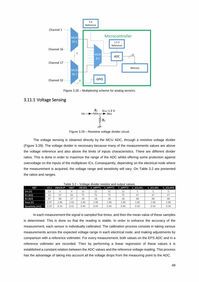
49
MUX8:1
MUX16:1
MUX16:1
ADC
Channel 1
Channel 16
Channel 32
Channel 17
GPIO4
4
Microcontroller
1.5 VReference
3 VReference
Memory
12
Figure 3.28 – Multiplexing scheme for analog sensors.
3.11.1 Voltage Sensing
Vin MuxVOUT ≤ 3 VR1
R2
Figure 3.29 – Resistive voltage divider circuit.
The voltage sensing is obtained directly by the MCU ADC, through a resistive voltage divider
(Figure 3.29). The voltage divider is necessary because many of the measurements values are above
the voltage reference and also above the limits of inputs characteristics. There are different divider
ratios. This is done in order to maximize the range of the ADC whilst offering some protection against
overvoltage on the inputs of the multiplexer ICs. Consequently, depending on the electrical node where
the measurement is acquired, the voltage range and sensitivity will vary. On Table 3.2 are presented
the ratios and ranges.
Table 3.2 – Voltage divider resistor and output values. NET V3.3 VBACKUP VBAT VBUSES V_MPPT1 V_MPPT2 V_MPPT3 V_SOLAR1 V_SOLAR2 V_SOLAR3
Vin [V] 3,6 5 9 15 15 15 15 5 5 5
R1 [KΩ] 10 47 56 75 75 75 75 47 47 47
R2 [KΩ] 47 68 27 18 18 18 18 68 68 68
Vout [V] 2.97 2.96 2.93 2.90 2.90 2.90 2.90 2.96 2.96 2.96
Sensitivity [mV] 0.29 0.34 0.41 0.44 0.44 0.44 0.44 0.34 0.34 0.34
In each measurement the signal is sampled five times, and then the mean value of these samples
is determined. This is done so that the reading is stable. In order to enhance the accuracy of the
measurement, each sensor is individually calibrated. The calibration process consists in taking various
measurements across the expected voltage range in each electrical node, and making adjustments by
comparison with a reference voltmeter. For every measurement, both values on the EPS ADC and in a
reference voltmeter are recorded. Then by performing a linear regression of these values it is
established a constant relation between the ADC values and the reference voltage reading. This process
has the advantage of taking into account all the voltage drops from the measuring point to the ADC.

50
3.11.2 Current sensors
All the current sensors used in the EPS follow the same principle of measuring the voltage drop
across a sensing resistor in series with the signal. This voltage drop is then amplified and sent to the
ADC. One of the used current amplifier sensors used is the INA139 Integrated Circuit from Texas
Instruments, whose circuit diagram is presented in Figure 3.30.
Figure 3.30 – Current sensor diagram [20].
This IC is suited for application, due to its electrical characteristics and to its small package
(SOT-23-5). The main electric characteristics are low quiescent current (60 µA), minimum voltage supply
of 2.7 V (it will operate at 3.3 V). It also allows configuring the signal gain through an external resistor.
The output signal is connected to one of the multiplexers input. To eliminate high frequency noise a
small capacitor is paced at the output.
Figure 3.31 – General current sensing circuit.
The current sensors used in the Power Distribution Module (PDM) do not need a sensing
resistor. In this module the current limiter itself has an internal sensing resistor which is accessible
through a pin on the IC as shown in Figure 3.32. For more details on the current limiter please see annex
A1.

51
Figure 3.32 – PDM current sensing circuit.
For sensing the battery current, although the method is same, the Integrated Circuit amplifier is
different, because the battery will have both negative and positive current values, depending if the
battery is charging or discharge. This IC is an INA181 also from Texas Instruments. It needs an external
reference (1.5 V), preferably half the voltage reference of the ADC (3 V). This way the amplifier offsets
the output voltage to 1.5 V and if the voltage is above this value, the current value is positive and vice-
versa. Figure 3.33 presents the current sensing circuit for the battery. As the gain is high (gain set to
50), the input noise is attenuated by the filter composed of the resistors and capacitor across the sensing
resistor, improving the Signal to Noise Ratio (SNR) at the output of the amplifier.
Figure 3.33 – Battery current sensing circuit.
The following table presents the characteristics of the current sensors measurements.
Table 3.3 – Current sensors characteristics.
NET General I_BAT
I [mA] 2000 1500
Vout [V] 2,000 3,000
Sensitivity [mA] 0,73 0,73
Again, for better measurement results the same procedure that is applied to the voltage sensors
is also applied to the current sensors both calibration and reading procedures.

52
3.11.3 Temperature Sensors
The microcontroller has an internal temperature sensor. In addition, the EPS also features
another temperature sensor IC (LMT87). The EPS also has to be able to read four more temperature
sensors, one from each cell of the battery. These temperature sensors are 10 kΩ NTC thermistors. In
order to read the temperature, a voltage reference of 3 V is used to drive the supply lines of a resistor
divisor. Because the thermistors are referenced to the negative terminal of the battery a 10 kΩ is used
between the voltage output and the reference voltage.
3 Vref ADC10 kΩ
- VBat
NTC
Figure 3.34 – Battery temperature sensing circuit.
The relation between the resistance and the temperature is presented in the Figure 3.35.
Figure 3.35 – Battery temperature sensors relation curve (Temperature Vs Output Voltage).
As shown in Figure 3.35 the relation is not linear, and a forth order polynomial regression relation
was used. The software converts the ADC values using the regression expression presented in the
figure.
3.12 Software
The software of the microcontroller manages the EPS. It periodically monitors the internal voltage
and current signals as well as the operating signals from the controllers of each module. It is able to
detect faults on the hardware and try to solve them by engaging redundant circuitry. Besides the system
monitoring, the EPS also communicates with the OBC, receiving commands for data logging,
diagnostics and power control of other subsystems. The EPS also reports single events, errors and
y = -10,235x5 + 89,802x4 - 296,9x3 + 457,15x2 - 355,07x + 161,07R² = 0,997
-50
0
50
100
150
200
0 0,5 1 1,5 2 2,5 3 3,5
Tem
per
atu
re [
ºC]
Output Voltage [V]
Temperature Vs Output Voltage Polynomial Fit

53
change of operation modes. Along with the power control, measurement routines and communication
routines, the microcontroller also handles the algorithm to drive the MPPT, as seen in section 3.1.4.
The microcontroller can only perform the aforementioned features one at the time. Some functions
must be deployed upon an event, others are periodical and others can be called whenever the
microcontroller is free without any priority privileges. To help facilitate the processor occupancy and
function time management, the software uses the internal timers to keep the main functions periodical
and Interrupt Service Routines to access the prioritized event, such as flag signals from the controllers
of the converters (buck, battery charger).
The software also employs four operating modes: Initialization mode, Safe mode, Normal mode
and Low Power Mode (LPM). Each operating mode defines the EPS power settings, and energy
management regime. When the processor of the microcontroller is not needed, the microcontroller
enters into LPM3, which means that it turns off the processor but all peripherals of the microcontroller
maintain full functionality.
The software or processor may fail. To prevent the EPS from being inactive the microcontroller
watchdog timer is used to reset the EPS. The OBC is constantly sending requests for the EPS, and if
the EPS does not respond the OBC can reset the EPS via the reset pin available at the PC104 bus.
The language used to program the software of the microcontroller is C.
3.12.1 Functions Overview
The main function is the first function that is called and stays running in an eternal loop inside
this function. Just before the infinite loop there are some functions that are called to configure the EPS
hardware and settings. Then it enters in the loop where it calls the other principal functions. As stated
these functions are periodical, and although they are called in the main, they are not enabled unless the
flag that is keeping the function from being called is set. For each one of the four functions there is a
timer which generates an interrupt. When the interrupt is triggered it enters into the ISR, resets the timer
and sets the flag of the respective function, enabling the function to be called and thus the periodic
timing is achieved, this functioning scheme is represented in Figure 3.36. There are four principal
functions that are called from the main function. The updateSensors function collects all the sensor
measurements (current and voltage and temperatures), except for the sensors concerning the solar
panels. Regarding these sensors, the measurement readings are updated by the mpptModules function
due to the flow procedure of the MPPT algorithm. As stated, the MPPT converter operates in two modes,
MPPT and Boost. So the function mpptModules also manages the decision between these modes. If
the satellite is in the eclipse, the MPPT converters are OFF.

54
Resets Flag
Begin Program
MPPTflag
Sensorsflag
Energyflag
Low Power Mode 3
Setup Hardware
Set EPS default Settings
Sensors Flag State
MPPTFlag State
EnergyFlag State
Energy Timer ISR
MPPTTimer ISR
comm Flag
comm Flag State
I2C Receive ISR
SensorTimer ISR
Sets Flag
Sets Flag
Sets Flag
ADCReady ISR
epsEnergy
updateSensors
mpptModules
communication
Module Error ISR
Resets Flag
Resets Flag
Resets Flag
ISR?
Yes
No
Yes
No
Yes
No
Yes
No
YesNo
Infinite loop
main
Figure 3.36 – "main" function flowchart.
When the processor is needed it shuts off, putting the microcontroller into Low Power Mode 3.
The microcontroller should only go to this mode when it finishes the aforementioned principal functions
and no interrupts were generated. The microcontroller goes into normal mode upon a generation of an
interrupt.
The communication handles the communication between the EPS and BC via the I2C bus. This
function also performs the received commands.
The epsEnergy chooses when to charge the battery, supply or cut the power to the subsystems
(by activating the electronic switches), enable/disable the controllers of the converters and MPPT,
multiplexer switches, taking into account the energy that is produced versus the energy that is being
consumed. This task also performs auto-diagnostics, checking the power output, power rails, state of
charge of the battery, ensuring that all components are working. In case of component failure this task
engages the necessary bypass or alternative circuitry. Figure 3.37 shows the major procedures for each
operation mode. The EPS mode selection criteria is described in the next section.

55
epsEnergy
EPS mode select
InitializationMode
SafeMode
NormalMode
Low PowerMode
S\C sub-systems ON
Sensor Measurements
EPS ModulesReset
MPPT & Battery Charger
MPPT &Battery Charger
Redundant systems / Reset
Module
PAYLOAD OFF
Diagnostics
Errors?
MPPT
Hardware Module error?
Switch OFF Module
30 minute Timer
Set Latch circuit/ Write Flash
Sattelite Initialized Allert
All Sub-systemsOFF
MPPT &Battery Charger
EPS circuitry OFF
Measure SoC
Sensor Measurements
Hardware Module error?
Switch OFF Module
All System ON
SoC < 35%
Allert OBC SoC
Send Report to OBC
Sensor Measurements
Figure 3.37 – Operation modes procedures.
Another important function is the mpptModules whose purpose is to drive the MPPT converters.
It performs the MPPT algorithm, does the required measurements, each the function proceeds and
adjusts the duty cycle on the output, to achieve the MPP of the solar panels.
3.12.2 Operation modes
When the S/C is deployed the EPS starts with the Initialization mode. This is the first mode the
microcontroller enters when it is powered on for the first time after deployment. Once it enters in this
mode all devices are ON except the PAYLOAD sub-system. It starts a 30 minute count-down, and during
this period the EPS cuts off the power to all sub-systems and just manages the power coming from the
solar panels with MPPT switching, and charges the battery.
Once the 30 minute period has passed, the EPS enters into safe mode powers up the
sub-systems and alerts the OBC indicating that the initialization sequence is over and that it is ready to
accept commands from OBC.

56
Finally if the monitor system does not report any errors nor low charge of the battery, the EPS
changes to the normal operation mode. The monitor takes readings from the current and voltage
sensors, from the controllers (buck and battery charger), and from the battery’s State of Charge. If the
system management reports any anomaly or if the battery charge is low, the EPS will remain in safe
mode until redundancy circuitry is engaged or if the battery has reached enough charge (above 40%).
In normal operation mode all the subsystems are powered ON, performing the tasks regarding to energy
control and management.
The operation mode may change into safe mode if the battery charge drops below 30%, or any
error occurs in the monitor sensor readings. In this case the EPS will first inform the OBC of the
occurrence before changing into safe mode.
To enter into low power mode, the system should be preciously in safe mode, and the battery
charge must drop down to 10%. In this mode all the subsystems are starved of power except the Beacon
subsystem, so that the battery can charge up. Before changing the operation the EPS will send a
message to OBC signalling the change of operation mode.
Figure 3.38 – Operating mode state chart representing the operation modes of the EPS.
In extreme cases, all the power may fail due to battery discharge, eclipse or component failure. If
any of these situations occur, when the power is restored the EPS still passes through initialization
mode, but it bypasses the timer entering straight into safe mode.
The sequences of different modes are presented in the diagram of Figure 3.38.
3.12.3 Interrupt Service Routines
The Interrupt Service Routines, as the name would suggest, interrupt the program in order to
service a routine. These ISR can be triggered by the timers, AD converter, GPIO and other peripherals.
When triggered the interrupts also wake up the processor within the microcontroller if it is in LPM3. The

57
microcontroller has timing mechanisms for each peripheral, but there is an actual timer dedicated to
manage the count down time. This timer triggers an ISR that in turn sets the flags for the other functions
addressed in 3.12.1, assuring that a periodic timing is achieved.
To keep track of time, another timer is used. This timer increments a timestamp with a period of
250 ms. The EPS has no reference to determine the date or real time, as it does not need to. Instead it
deals with relative time stamps.
Another important ISR is from the ADC, which lets the program know when the conversion is
done. This mechanism frees the processor to do other procedures rather than standing by for a valid
measurement. Upon the interrupt the program resumes the processing of the measurements.
The communication is implemented with interrupts, meaning that the processor is not actively
waiting nor the program is constantly checking if there is any message available (polling).

58
Energy Budget
In this chapter the energy budget of the ISTsat One is analysed according to the EPS power figures
and the total power consumption of the satellite. Firstly the energy generation from the solar panels and
power generation evolution over an orbit must be considered, with the proposed EPS architecture.
Secondly the power budget of the satellite and the energy budget are calculated, allowing the
comparison of the total produced energy versus the energy that is consumed over an orbit. This study
is of particular importance in order to make sure that the satellite is self-sustained, in terms of energy
and that it is capable of performing its mission without any power failure.
4.1 Expected Energy Generation
Using solar panels chosen with 1 U cubesat format and made by standard photovoltaic triple junction
cells, the maximum electrical power that can be generated is approximately 2400 mW. This power can
be theoretically achieved with the aid of a Maximum Power Point Tracking converter, and with 100% of
efficiency. However, in practice, the efficiency of this electronic circuit is, for small power ranges,
between 85% and 90%, so its loss is about 10% to 15% of the maximum available power.
As an example, for a standard 1U solar panels made with two Spectralabs triple junction solar
cells with 32 cm2 of area (see reference [6]), connected in series, the maximum power generated in
AM0 sun irradiation conditions, at 25 ºC is 0.9 x 5.33 V x 0.544 A = 2.61 W, adjusting its load to the
optimum value according to (1) (see page 30). At 45 ºC degrees this power decreases to 2.49 W due to
the decrease of OCV at a rate of -12 mV / ºC.
Normally the available power is smaller because it needs to be multiplied by cos(α), where (α)
is the angle between the face of the panel and the plane perpendicular to the Sun beam. In practical
terms only the area of solar panels projected on this plane account to the energy recovered.
For a cube covered by solar panels, the area projected over this plane is maximum when a cube
vertex points to the Sun. In this case the shape of this area is a hexagon with an area that is 1.73 larger
than the area of the cube face. The recovered maximum electrical power, at a panel temperature of
45 ºC, will be 1.73 x 2.49 W = 4.3 W. However this is not a common satellite orientation because usually
this orientation is imposed by the mission to be accomplished.
In a satellite orbit, similar to the ISS orbit, and with the satellite controlled to maintain the –Z
face oriented to the earth centre, the power recovered at 25 ºC temperature ranges between 2.61 W
(only one face pointing to Sun, over equator), 3.69 W for two cube faces oriented towards the Sun,
(1.4 x 2.61 W = 3.69 W), and 5.53 W when 3 faces of the cube are symmetrically oriented to the Sun.
During eclipse no power is being generated. The duration of one ISS orbit is 92.7 minutes with
36 minutes in eclipse. The mean power generated during a complete orbit will be the mean power
generated in the satellite under sunlight multiplied by the ratio of the sunlight time to the orbit time,
57 minutes / 93 minutes = 0.61.
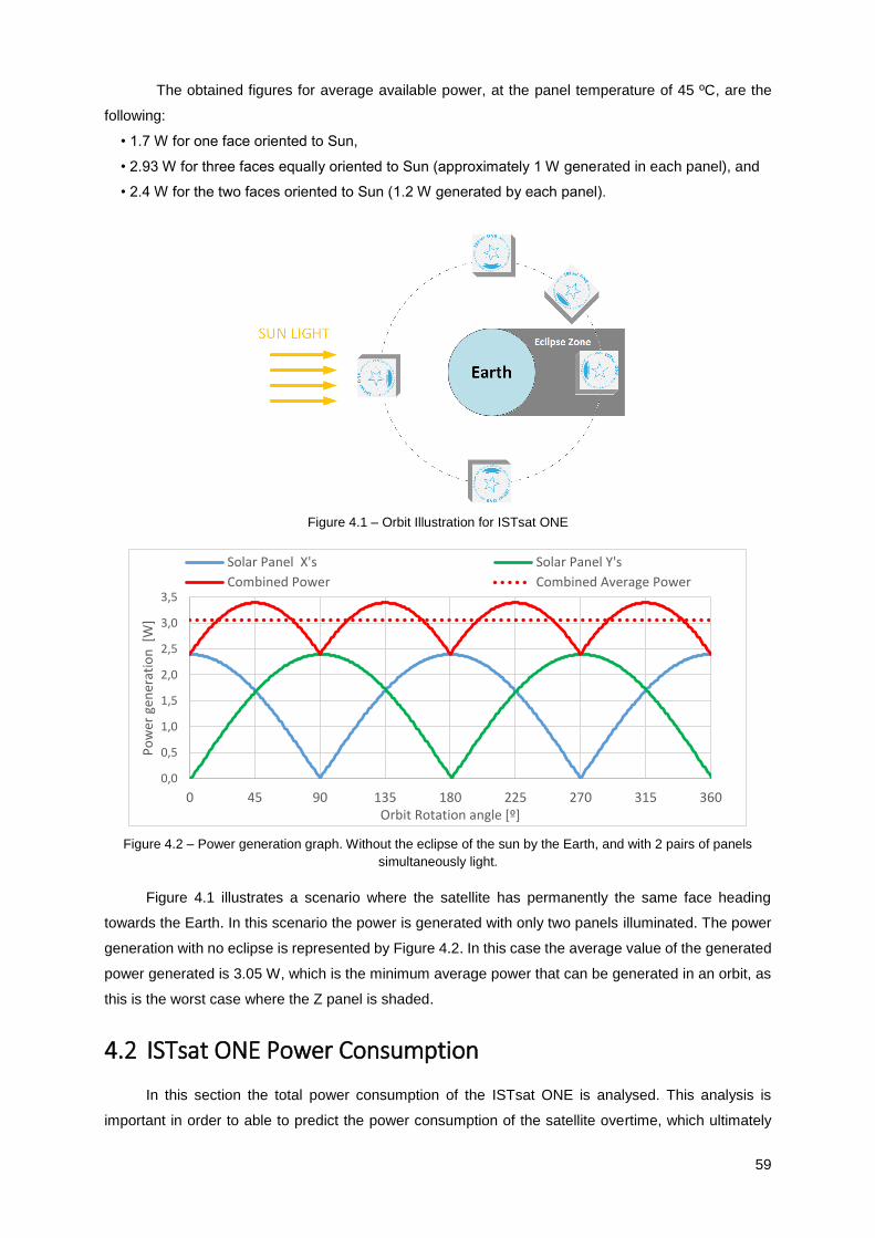
59
The obtained figures for average available power, at the panel temperature of 45 ºC, are the
following:
• 1.7 W for one face oriented to Sun,
• 2.93 W for three faces equally oriented to Sun (approximately 1 W generated in each panel), and
• 2.4 W for the two faces oriented to Sun (1.2 W generated by each panel).
Figure 4.1 – Orbit Illustration for ISTsat ONE
Figure 4.2 – Power generation graph. Without the eclipse of the sun by the Earth, and with 2 pairs of panels
simultaneously light.
Figure 4.1 illustrates a scenario where the satellite has permanently the same face heading
towards the Earth. In this scenario the power is generated with only two panels illuminated. The power
generation with no eclipse is represented by Figure 4.2. In this case the average value of the generated
power generated is 3.05 W, which is the minimum average power that can be generated in an orbit, as
this is the worst case where the Z panel is shaded.
4.2 ISTsat ONE Power Consumption
In this section the total power consumption of the ISTsat ONE is analysed. This analysis is
important in order to able to predict the power consumption of the satellite overtime, which ultimately
0,0
0,5
1,0
1,5
2,0
2,5
3,0
3,5
0 45 90 135 180 225 270 315 360
Po
wer
gen
erat
ion
[W
]
Orbit Rotation angle [º]
Solar Panel X's Solar Panel Y's
Combined Power Combined Average Power

60
leads to the estimation of the energy that is needed to operate and carry out the mission. As referred
ISTsat ONE has four operating modes, but only two can be accounted for, the safe and normal modes.
The other two modes do not perform any operation for the mission and are only triggered if there is any
power failure, besides the power consumption is very low.
There are many scenarios that can affect dramatically the power consumption. For starters, the
ISTsat ONE has five independent sub-systems, and each of them operate according external activities,
such as the numbers of airplane’s communications captured, how many contacts are established with
ground station, to name a few. To make an estimate of the power consumption some assumptions were
made following the most probable scenarios and some unfavourable situations. The Table 4.1 presents
the estimate values of power consumption for different ISTsat ONE subsystems for normal and safe
modes.
Table 4.1 – S/C Power Figures
Module Peak [mW] Average [mW] Normal Mode [mW] Safe Mode [mW] Notes
TTC Rx 400 300 60 30 1
TTC Tx 2000 750 83 60 2
Beacon Tx 300 175 66 66 3
OBC 500 320 64 60 4
COM 1500 750 156 60 5
Payload 1000 900 150 60 6
Magnetorquers 775 775 39 0 7
EPS 200 75 75 75 8
Battery Heaters 400 400 80 80 9
Total 7075 4445 773 491 10
Energy losses 3032 1905 331 210 11
Total + Losses 10107 6350 1104 701 12
Table 4.1 Notes:
1– TTC receiver in normal mode may be on all time thus consuming 300 mW, however it can be put into sleep
mode 9/10 of the time and the average power will be reduced.
2 – TTC power consumption of the transmitter is 2000 mW but is active only a maximum of 60 minutes per day,
on average. Indeed, one assumes a radio connection, in five passes of the S/C, over our main GS. Mean power
consumption is therefore 16.7 mW. In Safe Mode TTC transmitter is in a low duty cycle routine and only transmits
(short telemetry data) upon being solicited by the main GS.
3 – Beacon transmitter alternates with the TTC transmitter; the average power consumption is approximately
250 mW in linear mode however it can be used in class C and power consumption is about 175 mW for 125 mW
of carrier. Turning ON/OFF the Power Amplifier and transmitting the Morse message has an occupation time
(point/dash/ word) of 112.5 seconds. The period between each message is five minutes.
4 – OBC, including sensors with a duty cycle of 20% for housekeeping. In sleep mode the power losses are due
to maintaining I2C communication alive.
5 – the estimated mean value considering that the subsystem is all time ON COM working with ADS-B for data
processing storing information and 60 minutes of communication with the ground station. This is the worst case
for the payload consumption, because the payload may also transmit data to ground in the same orbit.
6 – ADS-B Payload estimation for 4 hours minimum of consecutive operation preprogramed by the ground
station.
7 – Magnetorquers (three) operating only 5% of time for normal satellite stabilization.
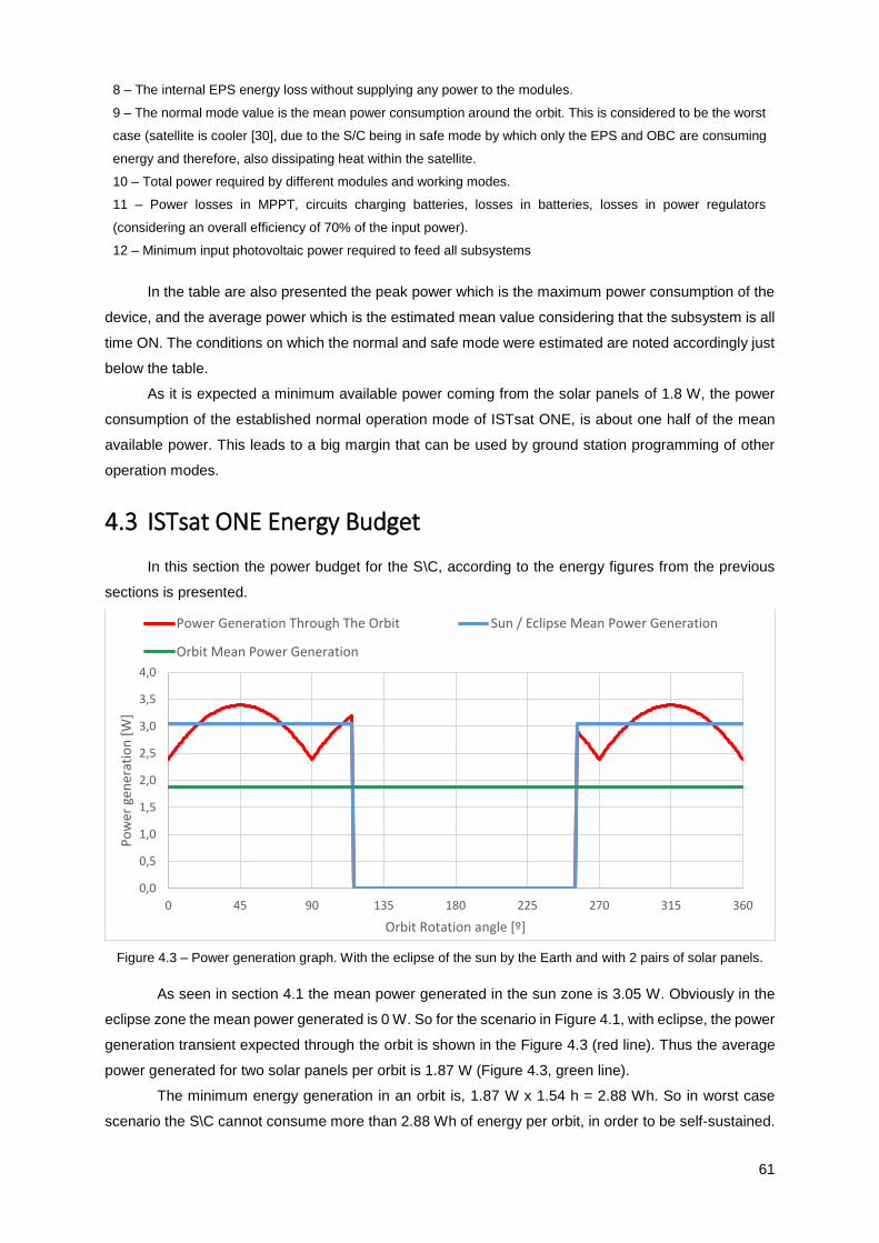
61
8 – The internal EPS energy loss without supplying any power to the modules.
9 – The normal mode value is the mean power consumption around the orbit. This is considered to be the worst
case (satellite is cooler [30], due to the S/C being in safe mode by which only the EPS and OBC are consuming
energy and therefore, also dissipating heat within the satellite.
10 – Total power required by different modules and working modes.
11 – Power losses in MPPT, circuits charging batteries, losses in batteries, losses in power regulators
(considering an overall efficiency of 70% of the input power).
12 – Minimum input photovoltaic power required to feed all subsystems
In the table are also presented the peak power which is the maximum power consumption of the
device, and the average power which is the estimated mean value considering that the subsystem is all
time ON. The conditions on which the normal and safe mode were estimated are noted accordingly just
below the table.
As it is expected a minimum available power coming from the solar panels of 1.8 W, the power
consumption of the established normal operation mode of ISTsat ONE, is about one half of the mean
available power. This leads to a big margin that can be used by ground station programming of other
operation modes.
4.3 ISTsat ONE Energy Budget
In this section the power budget for the S\C, according to the energy figures from the previous
sections is presented.
Figure 4.3 – Power generation graph. With the eclipse of the sun by the Earth and with 2 pairs of solar panels.
As seen in section 4.1 the mean power generated in the sun zone is 3.05 W. Obviously in the
eclipse zone the mean power generated is 0 W. So for the scenario in Figure 4.1, with eclipse, the power
generation transient expected through the orbit is shown in the Figure 4.3 (red line). Thus the average
power generated for two solar panels per orbit is 1.87 W (Figure 4.3, green line).
The minimum energy generation in an orbit is, 1.87 W x 1.54 h = 2.88 Wh. So in worst case
scenario the S\C cannot consume more than 2.88 Wh of energy per orbit, in order to be self-sustained.
0,0
0,5
1,0
1,5
2,0
2,5
3,0
3,5
4,0
0 45 90 135 180 225 270 315 360
Po
wer
gen
erat
ion
[W
]
Orbit Rotation angle [º]
Power Generation Through The Orbit Sun / Eclipse Mean Power Generation
Orbit Mean Power Generation

62
When the S\C consumption per orbit is lower than 2.88 Wh the excess of produced energy is stored in
the battery.
In Table 4.2 is presented the energy budget for the ISTsat ONE. This table is derived from Table
4.1 of the previous section, taking into consideration the energy losses, an orbit time of 1.54 hours and
a battery of 20.8 Wh.
Table 4.2 – S/C Energy Budget.
Energy Figures S/C in Safe Mode S/C in Normal Mode
Energy Generated / Orbit [Wh] 2.88
Consumed Energy without Losses / Orbit [Wh] 0.758 1.194
Energy Losses / Orbit [Wh] 0.325 0.512
Consumed Energy / Orbit [Wh]1 1.083 1.705
Energy budget / Orbit [Wh] 1.797 1.175
Orbits to Fully charge the battery2 7.5 11.4
Orbits until battery discharge3 without Energy Generation 19.2 12.2
On normal operation mode the S/C is self-sustained, as the energy budget is positive, which
means that 1.175 Wh can be directly stored in the battery. This means that if necessary the S/C can
perform extra events. Considering the event of the satellite being constantly draining the average power
continuously for each subsystem (see Table 4.1), the S/C is no more self-sustained, but it can maintain
this operation during 2 orbits, and then it has to switch back into normal operation. If fast battery charging
is necessary the S/C goes into safe mode operation, as this is where the energy budget is higher (1.797
Wh), taking up to 7.5 orbits to fully charge the battery.
In an extreme case if ISTsat ONE solar panels fail, the S/C can remain operational up to 19.2
orbits (29.6 hours) in safe mode operation, and 12 orbits (18.5 hours) in normal operation mode. Another
extreme case is the battery failure. In this case the S/C can only operate while it is out of eclipse. As
shown, the spacecraft produces enough energy to maintain the normal operation mode, but the energy
consumption cannot be considered as the mean energy, because it does not store the energy. And thus
the available power will vary according to Figure 4.3 (red line).
1 Energy consumption of the S\C plus the energy losses in the power conversion.
2 Considering that the battery (20,8 Wh) is fully discharge, and S\C has power consumption according to the respective modes.
3 From fully charge to fully discharged until approximately 0%, when on chip battery switches off, as it is not considered battery
charging the battery heaters are OFF, as the thermal analyses refer to an internal average temperature of -1,5ºC with an amplitude
variance of 1ºC within the satellite.

63
Testing platforms
During the development of the EPS, custom testing platforms were developed in order to
validate the EPS electrical specifications and to facilitate the testing interface. These platforms are the
automated measurement system and the FlatSat.
5.1 Automated Measurement System
The Automated Measurement System (AMS) was developed to facilitate the EPS and battery
testing and characterization. The AMS is composed by various electronic measuring instruments, which
are controlled by a computer through the General Purpose Interface Bus (GPIB). The instruments that
compose the AMS are presented in the Figure 5.1:
Figure 5.1 – Rack shelf containing the Instruments that compose the Automated measurement system.
(A - Switch / Control Unit – HP 3488A; B - Multimeter - HP 3458A; C & D - Multimeter - HP 3478A;
E - Programmable Power Supply - Philips PM 2812; F - Electronic DC load - HP 6050A).
In terms of supplying power, the system is capable of executing voltage sweeps and current
sweeps. This is useful to test the minimum voltages at which the EPS systems start to work as well as
emulating controlled voltage or current ripples at the inputs.
A
B
D C
E
F

64
The electronic load helps to set a load at the output of the testing modules. The load can be
with to a constant or variable values. The switch / control unit is composed by multiple matrix relay cards,
which helps to expand the multimeter ports to different measuring test points without any risk of
interference.
When testing the EPS the AMS setting consists only in the control of the power supply, set a
load (if necessary) and the measuring with the multimeter. At the same time the measurements are sent
to the computer for further processing.
The software to control the instruments was developed using G language, with National
Instruments LabVIEW software. The AMS is capable of performing many measurements, namely the
power efficiency, by measuring the input and output power (current and voltage), perform load sweeps,
load transients, power supply transients, supply sweeps both on voltage and current and data logging
(measure current, voltages, temperatures).
5.1.1 Battery Tester
One of the advantages of this system is the flexibility of the instruments remaining set. In fact
only the connections to the testing device and program need to be changed to accommodate the test
procedure. The battery tester was developed to obtain each battery cell capacity and charging /
discharging profiles, while monitoring the temperature at each step. It can also determine the internal
resistance of each cell. The circuit wiring of the AMS and connections for testing a battery or cell is
presented in Figure 5.2.
PC
National Instruments
NI-488.2
AmmeterHP3478A
A+ -
Switch / Control Unit
HP 3488A
VoltmeterHP 3478A
V
+
-
OhmmeterHP 3458A
Ω
PhillipsPM-2812
PCM
Varta LPP 503759 8HH
NTC
+
-
NTC1
NTC2
NTC3
NTC4
USB
Electronic DC LoadHP6050A
LOAD
Figure 5.2 – Connections diagram of the AMS with a battery cell.
As mentioned the battery pack is a 2S2P cell configuration, so after assembly the battery pack
is also tested to verify if it is within the specifications. So, the battery tester lets the user configure the
maximum charging voltages as well as set the minimum voltage of discharge. Because the cells can
have a parallel connection the current can also be set by the user, both discharge and charge. The
current and voltages range of values is limited by software. While discharging the current cannot be set

65
above 1.5 A and the voltage below 3 V. For charging the maximum current is also 1.5 A but the voltage
is 8.4 V.
The battery characterization is conducted under a controlled temperature environment. But the
battery cells may also generate heat. So, the battery tester is constantly monitoring the cells voltage,
current and temperature. If any of the variables are out of specification the battery tester stops the
program immediately, by resetting all instruments with the respective outputs OFF. For charging, the
temperature must be above 0º C and below 45 ºC. When it is discharging, if the temperature falls below
-10 ºC or is above 45 ºC, the program stops the current testing.
The program allows the user to choose among various functions: a full characterization; a
discharge profile; the determination of the internal resistance of the cell or battery; or simply just charge
the battery. At the end of each procedure the program stores all the logged data in an excel type file
and prompts the user with the saving location.
The discharging profile is obtained by logging the voltage over time with the DC electronic load
set to constant current mode (with the pre-set discharge current). The current through the battery is also
recorded during the discharge. So by calculating
∫ 𝑖(𝑡)𝑡
0𝑑𝑡 , (23)
at the end of the discharge with t being the lapsed and with i(t) being the current function over time, the
total discharged charge is calculated. Hence in order to obtain the full capacity of the battery, the battery
should be fully charged before starting this procedure. Another important note to have in mind is that as
higher current rates occur during discharge, the higher is the difference between OCV and the voltage
on the battery terminals, as seen in section 3.4. Thus at the end of discharge the discharge current
should be lowered so that the battery voltage does not decrease below its limit.
To obtain the internal resistance profile versus the voltage of the battery, the program used is
similar to the discharge profile, but with an added difference. The procedure is effectively the same as
described in section 3.4. But in order to obtain the batteries internal resistance while discharging, bursts
of higher current rate are applied in order to have a different current value. Through (20) is possible to
obtain the internal resistance. The OCV in (20) is the voltage of the battery while in normal discharge.
Then, by applying a higher current burst and measuring both voltage and current during the higher
current period, through (20) the internal resistance is obtained. The following flowchart displays the
procedure.
Begin
VBAT < VDISCHARGE
Apply constant current load to
battery
Done
Apply higher current to battery
MeasureVoltage (V1)Current (I1)
MeasureVoltage (V2)Current (I2)
Yes
No
Figure 5.3 – Internal Resistance Measurement with current pulses.

66
As previously mentioned the internal resistance of the battery also varies with temperature. In
order to acquire this relation, the same procedure, presented in Figure 5.3, is done at different
temperatures.
5.2 FlatSat Board
The FlatSat board was developed with the purpose of testing and debug each sub-system of the
ISTsat ONE. As the name would suggest, the idea is to assemble the satellite in a flat, horizontal way
with each subsystem board mounted on a FlatSat PCB. The satellite is assembled in this way first, in
order to thoroughly test all hardware and software whilst maintaining the ease of access to every
subsystem for probing signals or debugging.
This board fits on all the satellite sub-systems and these boards can be connected to others
through the 96 pin DIN connectors. The signals passing through these connections are the ISTsat ONE
PC104 bus. Another feature of this board, is that it is able to isolate specific signals from each sub-
system to the satellite main bus through jumper connectors. To facilitate the debugging, each board
breaks out every signal from the PC104 and make it available in the additional header pins next to the
jumpers.
The EPS is the sub-system that supplies power to satellite however, if the EPS is not present in
the FlatSat tests or is isolated, the rest of the boards can be supplied trough a power port available in
the FlatSat board. The LEDs inform which of the lines are active.
Figure 5.4 – Two FlatSat test boards for ISTSat-ONE Sub-systems interconneted.

67
EPS Prototype
The design and the EPS expected figures were presented through the previous chapters. Through
this chapter the individual testing circuit module, the outcome design of the EPS and the battery pack
are presented. It exposes the design challenges in order to have low Electromagnetic Interference (EMI),
whilst keeping the design compact enough to meet with the ISTsat ONE size envelope presented in
section 1.3.
6.1 EPS PCB Layout
The EPS prototype is presented in Figure 6.1. The board design follows strict design rules in order
to keep low EMI and to be compatible with the ISTsat ONE satellite. The board dimensions and cut out
line are mandatory as well as the placement of the PC104 bus connector. The screw holes also follow
the ISTsat ONE design rules.
Figure 6.1 – EPS prototype PCB (Left – Top View / Right – Bottom View).
This board has four electrical layers. The top circuitry is mostly dedicated to digital signals and
analog measurements. The circuitry which handles the power of the EPS (from the solar panels to the
final bus) is located on the bottom side of the board. Each layer is assigned to a specific type of signal:
top layer for digital signals; middle-top layer digital signals and analog signals; middle-bottom layer for
ground planes; bottom layer for power lines. To help reduce EMI the EPS features different ground
planes for different modules (see Figure 6.1).

68
Figure 6.2 – Middle-Bottom layer of the EPS PCB showing the ground planes.
The ground planes also help to organize the PCB design into specific areas corresponding to the
modules as seen in Figure 6.1. DC coupling capacitors are at every input and output of the modules, but
more critical are the capacitors that are placed near each IC power supply, in order to reduce input
noise. The microcontroller module features two ground planes, the analog plane and the digital ground
plane.
To help with EPS testing and debugging, test points were created all over the board to sample
voltages and currents. Regarding the components, whenever possible, space grade components are
used, if not available on the market military or automotive grades are used.
6.2 Battery Layout
The ISTsat ONE battery pack is composed of three boards. The main board is mounted at the
bottom and is where all the battery circuitry is placed along with the cells terminals. It also provides the
interface connection to the EPS.
Figure 6.3 – Picture of the ISTsat ONE Battery Pack. (Left - Top view; Right - Bottom view).
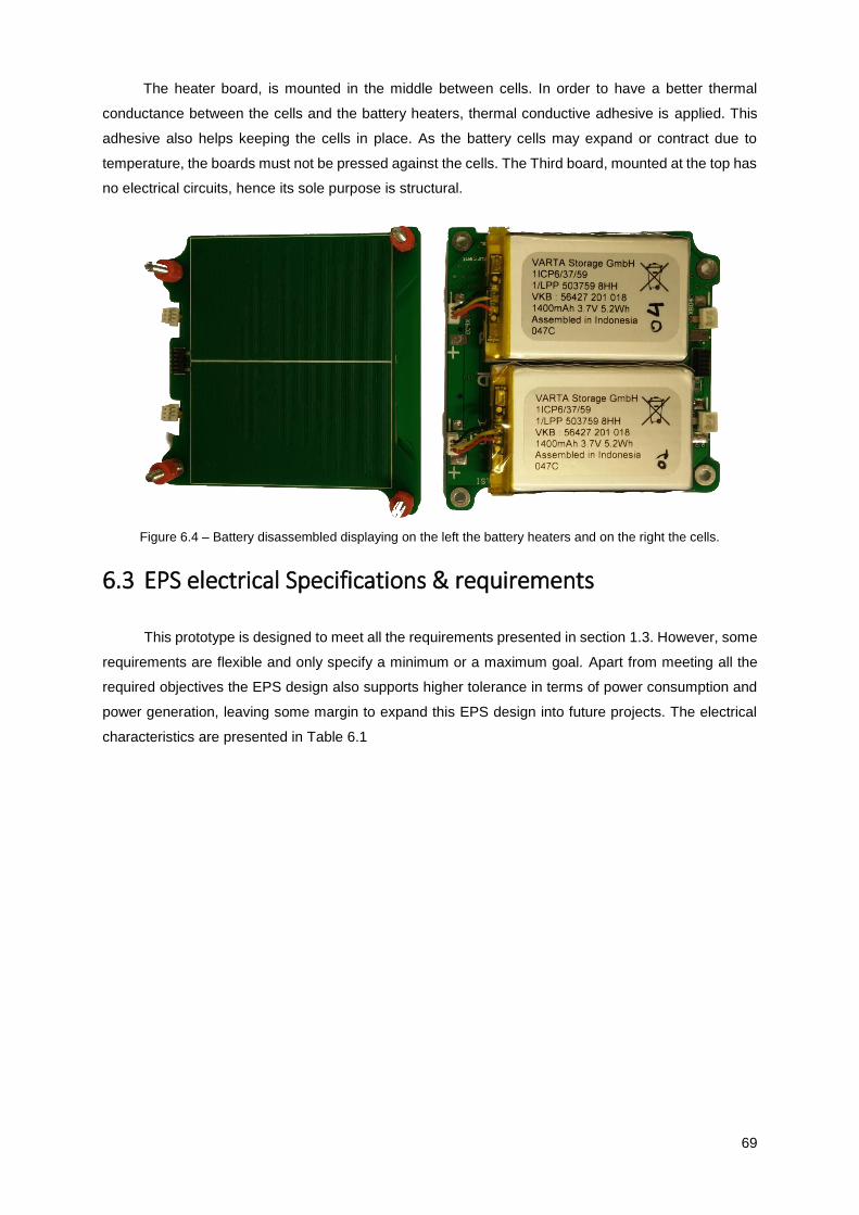
69
The heater board, is mounted in the middle between cells. In order to have a better thermal
conductance between the cells and the battery heaters, thermal conductive adhesive is applied. This
adhesive also helps keeping the cells in place. As the battery cells may expand or contract due to
temperature, the boards must not be pressed against the cells. The Third board, mounted at the top has
no electrical circuits, hence its sole purpose is structural.
Figure 6.4 – Battery disassembled displaying on the left the battery heaters and on the right the cells.
6.3 EPS electrical Specifications & requirements
This prototype is designed to meet all the requirements presented in section 1.3. However, some
requirements are flexible and only specify a minimum or a maximum goal. Apart from meeting all the
required objectives the EPS design also supports higher tolerance in terms of power consumption and
power generation, leaving some margin to expand this EPS design into future projects. The electrical
characteristics are presented in Table 6.1

70
Table 6.1 – Electrical characteristics of the EPS.
Parameter Conditions Min Typical Max Unit
Solar Panel X (connector PE3; PE4) Voltage 0 6 V Current 0 1 A
Solar Panel Y (connector PE5; PE11) Voltage 0 6 V Current 0 1 A
Solar Panel Z (connector PE1) Voltage 0 6 V Current 0 1 A
+3.3V (H2.27, H2.28)
Voltage output with EPS working 3 3.3 3.6 V Voltage output with EPS off 3 3.6 V Current Draw 3 A
VCCx (H1.47; H1.48; H1.49; H1.50)
EPS working 3 3.3 3.6 V EPS off 3 3.3 3.6 V Current Draw per output 1.5 A Current Draw all outputs combined Two Bucks ON 6 A
VCHARGE (H1.23)
Voltage Input through the charging port With RBF pin inserted
5 9 20 V Current Draw 0.23 0.5 0.9 A Voltage Input through the charging port Without the RBF and switches
deployed (satellite deployed) 5 14 V
Current Draw 0.26 0.6 A
VBAT (H2.45, H2.46)
Battery Output Voltage 6 8.4 V
Current Draw 2.4 A
VBACKUP (H1.42)
PV voltage output 0 5.8 V
Current Draw Note that the max current is
dependent by the solar exposure
0 1.5 A
Power Output Power distributed evenly
through two bucks 19.8 W
Power Consumption
Deployment switches pressed and RBF Inserted
0.9 24 mW
RBF pull pin removed and deployment switches released
100 150 mW

71
EPS Performance
To fully address all hardware issues, tests were made into each individual module. However there
are converters that are repeated or virtually the same, so some of the results are not mentioned in order
to keep this document clear. The following order of tests intends to follow the power flow throughout the
EPS, from the source of energy (solar panels) until the final outputs (PC104 power lines). This way is
easier to understand the implications between modules and eventually rule out possible issues.
7.1 Analog Sensors
Some of the results presented in this chapter were obtained by logging the sensor values from
the EPS, so it is imperative to understand the errors that are associated with these measurements. It
also validates the EPS measurements, thus taking the right effect when making the decisions
concerning the energy management, MPPT, SoC among others. Tables 7.1, 7.2 and 7.3 present the
errors associated to the measurements acquired from the EPS sensors.
Table 7.1 – EPS voltage measurement associated errors.
NET VBACKUPx V_SOLARx V_MPPT VBAT VBUSES 5V VCCx
Range [V] 6 5.07 14.33 9.301 15.50 5.073 3.639
Absolut error [V]
0.010 0.015 0.030 0.017 0.030 0.012 0.008
Table 7.1 figures were obtained by comparing the values read by the EPS with the same
instrument that was taken as reference for calibration, HP 3458A multimeter. These errors are mostly
associated with the quantification level and noise generated by the converters.
Table 7.2 – EPS current measurement associated errors.
NET I_BACKUP I_SOLAR I_MPPTx I_BAT I_BUSES I_VCCx
Range [A] 3 3 3 1.5 3 3
Absolut error [A] 0.012 0.012 0.020 0.005 0.005 0.005
The values in Table 7.2 were also compared and calibrated with the aid of the instrument HP
3458A as an ammeter reference. In this case the errors are also associated with the noise generated in
the current sense amplifiers and because of the high gain set by the amplifier, which in turn also amplifies
the input noise, reducing the signal to noise ratio. The temperature sensors from the microcontroller and
the EPS PCB are already calibrated by the manufacturer.
Table 7.3 – EPS temperature measurement associated errors.
NET Microcontroller EPS PCB Battery Cellx
Range [ºC] [-40 , +105] [-50 , 150] [-20 , +60]
Absolut error [ºC] 0.5 0.6 1

72
7.2 MPPT Converter
The MPPT converter was designed taken into account the power that it would generate, making
sure that the converter would present excursion in terms of duty cycle versus power, and that it should
remain within the Continuous Current Mode (CCM), since this mode is more efficient. Figure 7.1
presents the transient curves. As shown, the minimum power that will assure CCM is 246.5 mW. The
current flowing through the inductor presents a ripple of 140 mA of magnitude. Note that the conducted
tests did not have the battery connected to the output, so although the ripple is propagated to the output
voltage, it is not problematic because this converter is connected directly to the battery, which acts as a
huge capacitance and therefore the output voltage is stabilized.
Figure 7.1 – MPPT converter transient signals considering light radiance in the panels: Continuous Current Mode
(CCM) with an output current load of 173 mA (on the left); boundary between CCM and Discontinuous Current
Mode (DCM) with an output load of 52.5 mA (on the right).
While in MPPT mode the microcontroller has to able to process the MPPT algorithm as fast as
it can, meaning that the duty cycle adjustment period must be able to keep up with the light variance on
the solar panel, and thus affecting the MPP. The MPPT algorithm is processed 330 times per second
and is directly tied to the software complexity and to the number of tasks. This is also true while the
converter is in Boost mode. In order to see if the control implementation is fast enough and finds the
MPP, the algorithm convergence was tested and power transients were applied at both output and input
of the MPPT converter. Figure 7.2 presents the test results.
As shown below, the MPPT algorithm and converter work as previewed, it finds the MPP and
keeps adjusting the PWM accordingly to the maximum available power on the solar panel. The MPP is
tracked in less than 250 ms. The oscillations shown in the graph, result from the lack of PWM step
resolution and also some noise generated by the solar panels. Once the solar panels are connected the
MPPT starts working, and sets the initial duty cycle to 40%, this is done so that the MPPT converges
faster, by setting the duty cycle at the middle of excursion, which later depending on the MPP, the duty
cycle may increase or decrease. Furthermore, in a scenario where the battery has failed, the EPS can
only rely on solar power, so when it comes out of the eclipse zone, the EPS must be able to start if the
initial duty cycle is set to start with low factors (<10%) or high factors (>80%), the power generated at
the MPPT converter output during the first instants may not be enough, causing power failures. By
setting the initial duty cycle to 40% this risk is reduced. Another feature that also reduces this risky event
0
100
200
300
400
500
600
0
0,5
1,0
1,5
2,0
2,5
3,0
3,5
4,0
0 5 10 15 20
Cu
rren
t [m
A]
Vo
ltag
e [v
]
Time [µs]
Gate Voltage Inductor Current
Input Voltage Output Voltage
0
50
100
150
200
250
300
350
400
0
0,5
1,0
1,5
2,0
2,5
3,0
3,5
4,0
0 5 10 15 20
Cu
rren
t [m
A]
Vo
ltag
e [V
]
Time [µs]
Gate Voltage Input Voltage
Output Voltage Inductor Current

73
is that, after a power recovery the EPS starts in safe mode, with all outputs OFF and minimum
consumption, giving time to track the MPP of the solar panels, and only after the MPP is tracked the
EPS powers the subsystems.
Figure 7.2 – MPPT convergence test.
The previous results validated the implementation of both the hardware and software. In this
section the performance of the MPPT is evaluated by connecting the battery (charge of 7.4 V) to the
output of the MPPT and by applying different light radiation through time to the solar panels. This way,
the MPPT converter has the load connected while the input power is altered.
Figure 7.3 – Radiation variance test to the converter in MPPT mode.
0
100
200
300
0
500
1000
1500
2000
2500
0 1 2 3 4 5 6 7
Cu
rren
t [m
A]
Vo
ltag
e [m
V]
Time [s]
Input Voltage Input Current
0
20
40
60
80
100
0
100
200
300
400
500
0 1 2 3 4 5 6 7
Du
ty C
ycle
[%
]
Po
wer
Inp
ut
[mW
]
Time [s]
Input Power Duty Cycle
-100
0
100
200
300
0
1000
2000
3000
4000
0 5 10 15 20 25
Cu
rren
t [m
A]
Vo
ltag
e [m
V]
Time [s]
Input Voltage Battery Current Input Current
0
20
40
60
80
100
0
100
200
300
400
500
600
700
0 5 10 15 20 25
Du
ty C
ycle
[%
]
Po
wer
[m
W]
Time [s]
Power Input Duty Cycle

74
Figure 7.3 presents the radiation variance, allowing to conclude that the converter is able to
handle the power variations of the solar panels, by keeping the track of the MPP, as shown by the power
and duty cycle curves. Note that while the solar panel is at maximum power, the converter is able to
produce enough energy to charge the battery.
Figure 7.4 presents a uniform input voltage sweep variance with the battery fully charged
(8.35 V). In this case the converter is in Boost mode and the battery is disconnected in order to avoid
influencing the output voltage. The converter has enough excursion for the input voltage to be as low as
1.150 V to maintain the output regulated. With this value the duty cycle reaches its maximum value of
88.6 %. When the output is regulated, the ripple reaches up to 400 mVpp, which is considerable. This is
due to the microcontroller not being fast enough and to the number of PWM steps being limited.
Fortunately this does not pose a problem since the battery will be connected and it stabilizes the output
voltage. Furthermore, the buck converters will also eliminate this ripple at the supply outputs.
Figure 7.4 – Input voltage variance test with the MPPT in Boost mode.
As referred this converter has to be able to extract the MPP of the solar panel whilst charging
the battery. The main feature to keep in mind is that it must meet the charging profile of the battery. This
means that while the battery voltage is below the charging voltage (8.25 V), this converter is in MPPT
mode. At this point the current has to be monitored in order not to exceed the desired 800 mA, maximum
charging current. This should never happen as each MPPT will not produce more than 2.4 W, and since
the minimum voltage of the battery is 6.2 V, the necessary charging power would be 4.96W. To perform
this test the battery is disconnected from the MPPT and at the output a variable load is applied. Figure
7.5 presents the transient for the output load variance test and thus the transition between Boost and
MPPT modes.
0
20
40
60
80
100
0
2
4
6
8
10
0 1 2 3 4 5 6 7 8
Du
ty C
ycle
[%
]
Vo
ltag
e [m
V]
Time [s]
Input Voltage Duty Cycle Output Voltage

75
Figure 7.5 – Transition between the MPPT and BOOST modes.
The tests are conclusive and show how the converter either regulates the output voltage to 8.25 V
or extracts the Maximum Power from the solar Panel. As the load increases the converter can no longer
maintain the 8.25 V and starts performing the MPPT algorithm. Note that between transitions (from
Boost to MPPT and vice versa), the duty cycle suddenly adjusts to meet the power demands. Both input
and output power share the same shape but with different offsets, due to the power losses.
Figure 7.6 presents the power efficiency for the MPPT converter with the input voltage set to 5 V
and a maximum current of 1 A.
Figure 7.6 – MPPT converter power efficiency.
As expected at low power, the MPPT is less efficient proving the purpose of applying bursts of
pulses in order to obtain higher peak power, rather than low average power. Overall the efficiency results
are good, with an expected efficiency of approximately 88.5% at 2.4 W, which is also the expected
maximum power of the solar panels presented in section 3.1.
0
20
40
60
80
100
120
3500
4500
5500
6500
7500
8500
0 5 10 15 20 25
Cu
rren
t [m
A]
Vo
ltag
e [m
V]
Time [s]
Output Voltage Output Current
0
20
40
60
80
0
200
400
600
800
0 5 10 15 20 25
Du
ty C
ycle
[%
]
Po
wer
[m
W]
Time [s]
Duty Cycle Input Power Output Power
0102030405060708090
100
0 500 1000 1500 2000 2500 3000 3500 4000 4500 5000
Effi
cien
cy [
%]
Input Power [mW]
BOOST
MODE
BOOST
MODE

76
7.3 Battery Charger
This module is part of the redundancy for charging the battery. This converter should be used if
the MPPT modules fail to regulate the proper voltage or current for the battery. The input voltage of this
module is dependable on the power harvested from the solar panels and MPPT’s output voltage. As
such, in Figure 7.7 is presented the input voltage sweep results in order to analyse the behaviour of the
converter throughout the input range, from 0 V to 15 V.
Figure 7.7 – Input Voltage sweep test from 0 V to 15 V.
As stated this converter is a SEPIC type, and as such it can either step up or step down the
output voltage regarding the input voltage, as it can be confirmed by Figure 7.7. When the controller of
the converter starts working, it regulates the output voltage to 8.224 V. Another important aspect to test
is to analyse if the converter is able to charge the battery even if the power is limited. Figure 7.8 presents
the test results where the input power is limited to 866 mW (2.476 V, 350 mA).
Figure 7.8 – Battery Chargers Input Power limited by current to 350 mA.
The battery current shows that the battery is being charged and so the test results show that the
converter is able to transfer the energy to the battery. As the input power is limited so will be the charging
current. In this case the charging current is limited to 116.07 mA due to the input power starvation, but
the converter is set to limit the output current to 650 mA. To ensure that the controller detects the
maximum charging voltage as well as limiting the charging current, a variable load is applied to the
0,0
0,5
1,0
1,5
2,0
0
2
4
6
8
10
0 2 4 6 8 10 12 14
Cu
rren
t [A
]
Ou
tpu
t V
olt
age
[V]
Input Voltage [V]
Output Voltage Input Current Output Current
-0,14
-0,12
-0,10
-0,08
-0,06
-0,04
-0,02
0,00
0
1
2
3
4
5
6
7
8
0 2 4 6 8 10 12 14 16 18 20
Cu
rren
t [A
]
Vo
ltag
e [V
]
Time [s]
Input Voltage Battery Voltage Battery Current

77
output setting various steps and sweeping the output voltage. Figure 7.9 presents the waveform results
for this test.
Figure 7.9 – Battery Charger Output Voltage load sweep test.
The results are as expected. The maximum voltage obtained is 8.224 V, and the maximum current is
635 mA. This test also validates its charging profile which meets the battery requirement: constant
current, when the voltage is below the maximum charging voltage and constant voltage as the maximum
charging voltage is reached. In this case the current depends on the charge of the battery.
Figure 7.10 – Battery Charger Power Efficiency results for different input voltages.
Figure 7.10 displays the results for the efficiency. The expected maximum power that can be
extracted from the solar panels is 3.6 W, so this value defines the maximum input power to the battery
charger. Because the MPPT output voltage is constantly changing, various input voltages were set for
the determination of the efficiency. As shown the most ideal curve is the 5 V input voltage, which for the
power expected is the one that maintains the highest efficiency. This converter is clearly less efficient
than the MPPT, which proves that this converter is a secondary means of charging the battery. While
the satellite is grounded this charger also charges the battery through the charging port, but in this case
the efficiency becomes less important. The supply voltage for charging can be between 2.4 V and 14 V
due to the Zener diode at the MPPT output, (see annex A12). The power supply should be rated at least
7 W.
0,0
0,2
0,4
0,6
0,8
1,0
0
2
4
6
8
10
3,0 4,0 5,0 6,0 7,0 8,0 9,0
Cu
rren
t [A
]
Vo
ltag
e [V
]
Output Voltage [V]
Input Voltage Input Current Output Current
0
20
40
60
80
100
0 0,5 1 1,5 2 2,5 3 3,5 4 4,5 5
Effi
cien
cy [
%]
Input Power [W]
Vin = 3.5 V Vin = 5 V Vin = 8 V Vin = 12 V

78
7.4 Battery
The cells that compose the battery are characterized in order to compare their characteristics one
to each other. The matching of the cells is done according to the obtained charge capacity and voltage
output at same temperatures. Figure 7.11 presents the typical characteristics for a battery cell for a
discharge and charge rate of 0.42C.
Figure 7.11 – Full discharge and charge cycle cell result profile (0.42C @ 28 ºC).
As mentioned earlier, the batteries behaviour is strongly dependent on temperature, affecting
the internal resistance and the available charge. Hence the batteries temperature also needs to be
controlled, so that the cells temperature remains constant throughout the entire characterization
process. Another aspect to have in mind is that by charging or discharging the cell, it generates its own
heat, thus the cells temperature has also to be controlled. Nevertheless, the total charge capacity
obtained in this test is 1294 mAh.
Figure 7.12 presents the characterization for the ISTsat ONE battery pack characterization, but
again, this test lacks from the necessary temperature control for the battery. The total charge capacity
obtained in this test is 2351 mAh
Figure 7.12 – ISTsat ONE battery pack discharge and charge profile results (0.33C @ 25ºC).
The battery pack heaters were tested and are working properly. The following table shows a
comparison between the designed figures and the results.
-0,8
-0,6
-0,4
-0,2
0
0,2
0,4
0,6
0,8
0
1
2
3
4
5
0 2000 4000 6000 8000 10000 12000 14000 16000
Cu
rren
t [A
]
Vo
ltag
e [V
]
Time [s]
Voltage Current
-1,5
-1
-0,5
0
0,5
1
1,5
0
2
4
6
8
10
0 5000 10000 15000 20000 25000
Cu
rren
t [A
]
Vo
ltag
e [V
]
Time [s]
Voltage Current

79
Table 7.4 – Comparison results for battery heaters (@3.3V).
Designed Tested
DC Resistance (Heater 1) [Ω] 42.6 51
Power on Heater 1 [mW] 255 210
DC Resistance (Heater 2) [Ω] 42.6 46
Power on Heater 2 [mW] 255 240
Total Power [mW] 510 450
Due to the PCB manufacturing dispersion the heaters produce less power than expected, but still
acceptable and would not present any problems for battery heating.
7.5 Deployment Switches, Remove Before Flight Cut Off
Circuitry and Initialization Latch Circuit (MUX Module)
The MUX module is where the power control really happens, because it can switch off both the
power coming from the solar panels and battery. These switches can only be actuated by the
microcontroller if the RBF pull pin is removed (see annex A5). After these switches, additional ones are
placed also to cut off power (deployment switches).
In this section the power cut-off switches mechanism is analysed, by considering all the possible
combinations between the switches’ states while measuring the EPS power consumption. The results
are presented in Table 7.5.
Table 7.5 – Power Cut-off switches validation results and power consumption.
RBF pin
Deployment switches EPS
Switch 1 Switch 2 Switch 3 Power State
Vin[V] Iin[mA] Pin[mW] Time to
Discharge1 [Days]
Inserted Pressed Pressed Pressed OFF 7.420 0.126 0.936 648
Removed X1 X1 Pressed OFF 7.420 0.127 0.940 645
Inserted Released Released Released OFF 7.420 0.985 3.311 83
Removed Pressed X1 Released OFF 7.420 3.250 24.12 51
Removed X1 Pressed Released OFF 7.420 3.250 24.12 51
Removed Released Released Released ON 7.420 12.35 91.62 6.3
Analysing the results in Table 7.5, power cut-off switches are working as expected, supplying
power only if all the deployment switches are deployed and the RBF pin is removed. The lowest power
consumption while it is OFF, is obtained if the deployment switch 3 is not deployed. This switch cuts the
power off from the battery through the negative terminal, denying the supply from the battery. If this
switch is deployed and all others are still cutting off, the consumption increases. This is due to the pull
up and pull down resistors and quiescent current of the controllers in the EPS. Removing the RBF pin,
1 Time to discharge if the battery is fully charged and with a Depth of Discharge of 70%

80
the power increases, only this time the microcontroller is ON but no power outputs are enabled. Finally,
removing all switches the EPS power consumption is obtained (with battery heaters OFF), which is
91.62 mW. An important aspect to consider is that the satellite may be grounded and stored, awaiting
launch for a long time. So if the satellite is stored it is also relevant to know if the charge in the battery
lasts long enough until the satellite is deployed. As shown, if the satellite is awaiting launch in the P-
POD it can hold up to 648 days without needing a recharge, note this charge is calculated with a Depth
of Discharge (DoD) of 70%.
The Latch Memory circuit is in the Power Mux Module and is commanded by the microcontroller
that sets it, and the RBF resets the latch state. The memory in this circuit is implemented with the energy
that is stored in the capacitors. It is natural to have a minimum current leak in all electronic circuits, so
a discharge test is conducted to evaluate how long this circuit can hold its state without any power
supply. The results of this test are presented in Figure 7.13.
Figure 7.13 – Latch memory discharge profile.
After setting the latch memory and then cutting off the power, the capacitors begin to discharge.
The maximum voltage threshold of the MOSFET guaranteed by the manufacturer is 2.3 V, for which the
time of discharge for the capacitors to reach this voltage is 119 minutes. Hence the Latch memory circuit
can easily hold the memory during an eclipse period, and easily surpasses the goal time of an orbit,
proving that the memory is held if a power failure should occur.
7.6 Buck Converters
There are four Buck converters in the EPS and all of them employ the same design circuit. To
simplify and to make the document more enjoyable to the reader only the Buck 2 converter is analysed
more extensively.
The first thing to be tested is the stability and behaviour of the buck converter to different voltage
inputs. This is important because the input is the VBUSES net (annex A2) which may be connected to
the battery or to the MPPT. Therefore both sources present a constantly changing voltage. Figure 7.7
presents the results for the input voltage sweep test with a 15.7 Ω resistor connected to the output.
90,0; 2688119,3; 2324
1000
2000
3000
4000
5000
6000
7000
0 60 120 180
Vo
ltag
e [m
V]
Time [min]

81
Figure 7.14 – Buck converter 2 (3.3 V) input voltage sweep with a 15.7 Ω resistor connected to the output.
As expected the converter is able to regulate the output voltage as long as the input voltage is
above 3.3 V (within the specified range of variation). Another important conclusion to take from this
experiment is the minimum input voltage necessary for the converter to start passing through energy to
the output, which is 2.779 V. At this point and until the input voltage is lower than 3.3 V, the converter
simply makes a direct connection between the output and input. When the input voltage becomes equal
or higher than 3.3 V the controller starts regulating the output voltage, resuming its power switching,
typical in buck converters.
The two next experiments presented in Figure 7.15 and Figure 7.16 serve to test the output
regulation stability under high loads and alternating load transients. Figure 7.15 presents the output load
sweep test for the buck converter 2 with the input voltage at 7.4 V.
Figure 7.15 – Buck converter 2 (3.3 V) output load sweep test with 7.4 V at the converter input.
As shown in Figure 7.15 the converter is able to maintain the intended output voltage regulation
with only a slight voltage drop of 220 mV under high DC currents. Figure 7.16 presents the converter
signals with a transient load applied to its output.
0,00
0,05
0,10
0,15
0,20
0,25
0
1
2
3
4
5
0 2 4 6 8 10 12 14
Cu
rren
t [A
]
Ou
tpu
t V
olt
age
[V]
Input Voltage [V]
Output Voltage Input Current Output Current
,0
1,0
2,0
3,0
4,0
5,0
0
1
2
3
4
5
6
7
8
0,0 0,5 1,0 1,5 2,0 2,5 3,0 3,5 4,0 4,5
Cu
rren
t [A
]
Vo
ltag
e [V
]
Output Current [A]
Input Voltage Output Voltage Input Current

82
Figure 7.16 – Buck converter 2 with a transient load applied (10 kHz, duty cycle 15%, High Current 900 mA, Low
Current 250 mA).
The test in Figure 7.16 emulates a constant load with higher current transients. As shown the
converter can regulate the output voltage with voltage drops of approximately 100 mV under high current
spikes, although there is a difference between the output and input currents shape. This means that
when these spikes occur, the converter takes time to react to these variations, as a consequence during
these periods the efficiency decreases.
The power efficiency of the buck converter 2 is presented in Figure 7.17, and the efficiency of
the converter can reach as high as 92 %, which is a good result meaning that the converter is well
designed. Note that the converter has higher efficiency for higher power outputs, which is also
favourable because for lower power output, the solar panels may be producing power in excess and so
this excess is stored in the battery, hence less energy is wasted.
Figure 7.17 – Buck converter 2 (3.3 V) Power Efficiency vs Output Power.
Comparing buck converters 2 and 3, both are regulated for 3.3 V but have different switching
frequencies. So the efficiency is also compared between these two converters for an input voltage of
7.4 V (Figure 7.18).
0,0
0,2
0,4
0,6
0,8
1,0
1,2
0
1
2
3
4
5
6
7
8
0 50 100 150 200 250 300 350 400 450 500
Cu
rren
t [A
]
Vo
ltag
e [V
]
Time [µs]
Input Voltage Output Voltage Input Current Output Current
0
10
20
30
40
50
60
70
80
90
100
0 1 2 3 4 5 6 7 8 9
Effi
cien
cy [
%]
Output Power [W]
Vin = 5.5 V Vin = 10 V Vin = 8 V

83
Figure 7.18 – Efficiency comparison between buck converters 2 and 3 (output 3.3 V) for an input voltage of 7.4 V.
It is clear that buck converter 3 is more efficient, so for the final revision of the EPS PCB, the
switching frequency of buck converter 2 should be lowered in order to become more efficient. Both can
even work at the same frequency and be synchronized, option that is supported by the converter
controller. The electrical characteristics measured for each converter are presented in Table 7.6.
Table 7.6 – Electrical characteristics for the buck converters.
Buck Converter
1 2 3 4
Nominal Voltage [V] 5 3.3 3.3 3.3
Measured OCV Voltage [V]1 5.183 3.481 3.477 3.257
Measured Min Voltage [V]2 4.982 3.269 3.294 Not
measured
Output voltage Ripple [mV]1 < 5 < 5 < 5 < 5
Peak Current [A] 2.5 4.2 4.3 Not
measured
Switch Frequency [kHz] 400 900 700 630
The buck converter 4 measurements for the current did not take place because the circuits
which this converter is supplying demand less than 400 mA, as such no probe current was taken into
consideration when designing the EPS, so an accurate measurement was not possible to obtain.
7.7 Power Distribution Module
This module serves the purpose of providing protection and redundancy to each voltage supply
of every sub-system. This module is supplied from Bucks 2 and 3 (see annex A10). It features current
limiting ICs as well as a MOSFET switch and a Low Dropout linear voltage regulator for each power
supply. One of the tests conducted is the load sweep at the output, meant to test if the current limiter
feature is functioning properly (Figure 7.19).
1 The value is measured as open circuit voltage
2 The measured value is obtained with converter at the maximum output current
0
10
20
30
40
50
60
70
80
90
100
0 1 2 3 4 5 6 7 8 9
Effi
cien
cy [
%]
Output Power [W]
Buck Converter 3 (Vin = 7.4 V @ 700 kHz) Buck Converter 2 (Vin = 7.4 V @ 900 kHz)

84
Figure 7.19 – OBC subsystem power supply output (VCC1) load sweep test.
Figure 7.19 shows the results of current limiter to the OBC subsystem. As expected the power
is cut off if the current goes above 1.4 A, and it keeps trying to restore the power if it is OFF. To restore
the power, the load current must fall under 1.2 A to keep the power ON. Figure 7.20 displays a closer
look at the period when the current is limited by shorting the output terminal to ground.
Figure 7.20 – OBC subsystem power supply output (VCC1) shorted to ground.
Analysing Figure 7.20 it is clear that the power is switched OFF during the current limiting
regime. Note that the current limiter resets its state periodically, every 130 ms, turning the power output
ON, to test if the load is over 1.2 A and if so, it switches OFF the power again and the cycle repeats until
the load current is under 1.2 A. This feature is useful because in the event of a failure in the
microcontroller, the subsystem stays powered even if has triggered the current limiter due to a single
event, and if the subsystem has indeed failed, the power losses in the power restarting process are
negligible. Furthermore when this happens the current controller signals a flag to the microcontroller to
make the decision of keeping restarting or stop supplying power to the subsystem. Another important
conclusion is that the input voltage does not break down, meaning that the current limiter is very fast
triggering the current protection and so the other subsystems will not be affected if one of the
subsystems should pull to much current.
The current limiter allows for a short period of time to go over the current threshold, having some
tolerance to short period current spikes. Every power output in the PDM of the EPS has a battery of
capacitors to help stabilize and smooth the voltage fluctuations. Figure 7.21 presents the results for a
high load transient at the output to the OBC subsystem, set with the input voltage from buck converter
2 (3.3V) with normal MOSFET switch.
0,0
0,5
1,0
1,5
2,0
0,0
1,0
2,0
3,0
4,0
0 2 4 6 8 10 12 14 16 18 20
Cu
rren
t [A
]
Vo
ltag
e [V
]
Time [s]
Input Voltage Ouput Voltage Output Current
0,0000,1250,2500,3750,5000,6250,7500,8751,000
0,0
1,0
2,0
3,0
4,0
0 100 200 300 400 500 600 700
Cu
rren
t [A
]
Vo
ltag
e [V
]
Time [ms]
Input Voltage Output Voltage Output Current

85
Figure 7.21 – OBC subsystem power supply output (VCC1) under heavy loads transient
As shown above the average voltage maintains the 3.3 V but the ripple has significantly
increased. This is also due to the fact that both MOSFET and current limiter have a resistance
associated and so the voltage drop from the input to the output of the PDM increases. Although the
displayed voltage ripple is within specs, the loads of the ISTsat ONE should not be higher than 700 mA,
hence the ripple is considerably diminished.
Each subsystem can be supplied by buck converters 2 and 3. In order to control these power
sources, for every subsystem there are two possible switches (MOSFETs and LDO) plus the cross feed
switch that controls the power supply between the buck outputs. Tests were conducted to each possible
supply combination of these switches and buck converters. Table 7.7 presents the output voltages
obtained under the maximum current (presented in Table 7.8) corresponding to the minimum voltage
values, and the open circuit voltage which correspond to the maximum values.
Table 7.7 – PDM Voltage output measurement results.
PDM Swtich
Converter
Output voltages [V]
3V3 PAYLOAD OBC COM TTC
Min1 Max2 Min1 Max2 Min1 Max2 Min1 Max2 Min1 Max2
Normal (MOSFET)
Buck 2 3.310 3.479 3.310 3.481 3.275 3.481 3.213 3.480 3.230 3.471
Buck 3 3.230 3.474 3.386 3.475 3.211 3.475 3.321 3.475 3.296 3.476
Backup (LDO)
Buck 2 - - 3.205 3.312 3.298 3.302 3.159 3.312 3.164 3.297
Buck3 - - 3.179 3.313 3.157 3.302 3.081 3.312 3.101 3.298
Cross-feed Switch between Buck converters output.
All the values presented in Table 7.6 are within the specified regulated voltage of 3.3 V (±10%).
Mind that the Backup connections pass through a low dropout linear voltage regulator, making the output
voltage for these cases to be lower than the Normal switch connection.
1 Measured with maximum load (highest current) permitted by the current limiter.
2 Measured as OCV with no load applied.
0,0
0,2
0,4
0,6
0,8
1,0
1,2
1,4
1,6
0,0
0,5
1,0
1,5
2,0
2,5
3,0
3,5
4,0
0 50 100 150 200 250 300 350 400 450 500
Cu
rren
t [A
]
Vo
ltag
e [V
]
Time [µs]
Input Voltage Output Voltage Output Current

86
Table 7.8 – PDM Maximum Current output measurement results.
Maximum Output Current [A]
3V3 PAYLOAD OBC COM TTC
1,469 1,481 1,480 1,489 1,456
Table 7.9 presents the power output according to Table 7.8 values and their minimum
correspondent voltage values in Table 7.7.
Table 7.9 – PDM Maximum Power output measurement results.
Maximum Output Power [W]
3V3 PAYLOAD OBC COM TTC
4,864 5,019 4,848 4,947 4,799
Comparing the output power values with the required specifications presented in section 1.3 the
EPS surpasses the minimum required power.
7.8 EPS Performance
In this final section the overall performance of the EPS is analysed, taking into account both
hardware and software. The next step, is to analyse how all the harware modules work together to
convert the energy haversted from the solar panels and supply power to the satellite. One simple
experiment is to connect two solar panles to each MPPT, mount the battery in the EPS and apply a load
to it’s outputs. Figure 7.23 displays the results of this experiment. The setup conditions are as follow:
battery connected to the EPS, X MPPT connect to a DC power supply limited to 4.4 V and current also
limited at 0.47 A, which gives a maximum power of 2.04 W; Y axis MPPT connected to another DC
power supply with the voltage limited to 2.2 V and the current limited to 0.23 A (see Figure 7.22) and
with a 30 Ω connected to the TT&C subsystem output (powered by buck converter 3 (3.3 V).
Figure 7.22 – DC power supply configuration, I(V) characteristic and power curve.
0
0,5
1
1,5
2
2,5
050
100150200250300350400450500
0 0,5 1 1,5 2 2,5 3 3,5 4 4,5 5
Po
wer
[W
]
Cu
rren
t [m
A]
Voltage [V]
X DC power supply I(V) Y DC power Supply I(V) Y Power X Power

87
Figure 7.23 – Overall EPS experiment with the battery mounted, two MPPTs generating power for power inputs
conditions set in Figure 7.22.
This experiment served to prove that the MPPTs can work simultaneously with minor
dependancies between them. The output power from the MPPT can oscilate, this is due to the way that
MPPTs are connected. Both MPPT converters will force their own MPP at the input, but these converters
are boosts, sharing the same load, hence the output voltage is dependant on the input voltage and vice
versa (for the same duty cycle). Thus the output voltage is constantly oscilating as each converter tries
to set their own output voltage ideal for their input MPP, causing the MPPTs to strugle to find a stable
situation where both MPPTs are at their MPP. Another oscilating factor is the characteristic of the DC
power supply, as this poses a great challenge for the MPPT algorithm. The I(V) characteristic of the DC
power supply is square shaped (Figure 7.22), and the transition between constant current or constant
voltage is abrupt, so the MPPT algorithm will sense a very high derivative difference in the power curve
0
100
200
300
400
500
600
0
2
4
6
8
0 50 100 150 200 250 300 350
Cu
rren
t [m
A]
Vo
ltag
e [V
]
Time [min]
MPPT Output Voltage X Input Voltage Y Input Voltage X Input Current Y Input Current
0
20
40
60
80
100
0
0,5
1
1,5
2
0 50 100 150 200 250 300 350
Du
ty C
ycle
[%
]
Po
wer
[W
]
Time [min]
Y Duty Cycle X MPPT Output Power Y MPPT Output Power X Duty Cycle
-300
-250
-200
-150
-100
-50
0
50
7,6
7,7
7,8
7,9
8
8,1
8,2
8,3
8,4
0 50 100 150 200 250 300 350
Cu
rren
t [m
A]
Vo
ltag
e [V
]
Time [min]
Battery Voltage Battery Current

88
and so when setting the PWM the step between the previous and the new duty cycle can be higher than
usual, make it difficult to find the MPP.
Note that when the battery reaches the End of Charge Voltage (ECV) the power output on the
MPPTs begin to fall because at this point the MPPTs will both change into Boost mode. Once in Boost
mode the MPPT converter that has higher voltage at the input dominates the output and sets the output
voltage accordingly to its own duty cycle. This causes the other converter with less power to enter in
Discontinued Conductance Mode, and so the duty cycle is no longer verified by (7).
The final experiment serves to analyse the EPS efficiency and is displayed in Figure 7.24. In
order to do this, the power is supplied into the X axis MPPT and a variable load (in continuous conduction
mode) is used to sweep the output load and thus the power. During this experiment the battery is not
connected, in order to provide energy to flow in and out of the EPS without it being retained in the
battery. The OBC subsystem power output was used to apply the load, which in turn is supplied by the
buck converter 2 (3.3 V).
Figure 7.24 – EPS Overall Efficiency with supply power in (5 V) through X axis MPPT, without the battery connected
and a variable load applied to the OBC subsystem output.
Note that during this experiment the MPPT remains in Boost mode, because the maximum
power is not required, and so the MPPT is able to regulate to 8.25 V. The overall efficiency of the EPS
is good, considering that two converters in series are used to achieve the necessary power output and
with the efficiency reaching as high as 82%. As expected the curve is similar to the efficiency graphs
from the previously studied converters and because they are in series it can be confirmed that the overall
efficiency is the product of both MPPT and Buck converters efficiency curves. Again the optimal
operation is at higher loads where the power is greater. But keep in mind that when the battery is
connected the demanded power from the solar panels will be higher, as it has to charge the battery
whilst supplying the power to the satellite. If the battery is fully charged, the power that is produced from
the solar panels and MPPT should be enough to power the satellite. Yet this case is where the EPS is
in disadvantage efficiency wise, it is not a problem since there is excess of energy.
While the satellite is at eclipse zone no power is being produced from the solar panels, hence
the battery must supply the power. In this case there is only one converter between the battery and the
outputs, meaning that in this case the efficiency rises.
0
10
20
30
40
50
60
70
80
90
0 0,5 1 1,5 2 2,5 3 3,5 4 4,5 5
Effi
cien
cy [
%]
Power Input [W]

89
Conclusion
The pre-thesis studies have involved careful analysis of the architecture and hardware that is to
be implemented to the EPS. Throughout the State of Art are presented the challenges and techniques
used to design an EPS are presented. These various approaches address the efficiency, size and
number of components used, and reliability. It also shows the ever growing market of the CubeSats and
their role, thus the importance of the standardization in nano satellites. This implies that the cost of
building a satellite is reduced, giving the opportunity of student projects such as the ISTsat ONE satellite
to be conceived.
A first version of the EPS for the ISTsat ONE was made but due to new features and requirements
of the ISTsat ONE, a new EPS has been designed in order to comply with all requirements. The
proposed architecture for ISTsat ONE EPS is similar to the architecture Maximum Power Point Tracker
and Battery Charge Regulated Bus, described in section 2.3.2.3, which is proven to work. The only
difference is that the battery can also be charged with a dedicated independent battery charger
controller, which is implemented separately from the MPPT.
As shown in Chapter 3 the architecture and design of the satellite is finalized taking into
consideration the solutions presented in the State of Art. This project involves both hardware and
software development. The software that is developed implements the MPPT algorithm, the energy
system management and communication to the other subsystems.
Another system that was developed during this work is the Automated Measurement System,
with the main purpose of characterizing and test the EPS hardware performance and the
characterization of the cells and battery for the ISTsat ONE. Unfortunately due to limited time and to the
work extension, one feature that still remains to be developed is the temperature control for the battery.
Because the battery does not feature the temperature control (cooling or heating) the results obtained
are not valid, because the temperature highly affects the battery performance. Thus the results for the
battery charge profile serve only as reference of what to expect in future measurements and to prove
the AMS functionality.
Following the power path from the source (solar panels and battery) to the power output (rails of
the subsystems) every single module is characterized and operates properly. The MPPT algorithm
converges in less than 250 ms allowing the EPS to perform the tracking even if the satellite is tumbling
heavily. In the case of the satellite being launched and forced into low power mode, the de-tumbling
system is not engaged but still EPS is able to keep tracking of the MPP and efficiently charge the battery.
The battery charger is working properly and can charge the battery reliably even if the power input is
lower than expected. The Power Mux module (RBF and deployment switches, Latch, battery and solar
power switches) is working well, meaning that the Latch can hold the initialization state for more than
one orbit time if there is a power failure. The RBF and deployment switches mechanism proven to work
and perform the intended logic. While the EPS is OFF, forced by the deployment switches, the power
consumption is very low allowing the satellite to be stored up to 600 days while waiting for launch.

90
All the Buck converters regulate the voltage in any circumstance, and the PDM monitors the
outputs and offers protection to the EPS and to the other subsystems, by limiting the output current and
even offering protection against short circuits. The extra regulators available in the power distribution
module offer redundancy for the power regulation if the buck converters should fail.
Regarding the EPS as a whole, it can manage the power between the battery and the solar panels
whilst supplying power to the subsystems. It manages to recharge the battery, if the solar panels harvest
enough energy, or the battery supplies the power to the satellite. All this happens seamlessly to the
subsystems. The overall efficiency is good reaching up to 82%. Part of this result is due to the fact that
the modules that compose the EPS are also very efficient, but other part is also due to the overall
architecture used to achieve the EPS requirements.
A study was made on the energy budget for the ISTsat, in order to predict if the energy harvested
from the solar panels is enough, if the battery charge capacity is adequate or simply analyse the overall
power consumption of the satellite. The conclusion was that with the new EPS architecture the ISTsat
ONE is self-sustained producing enough energy to power itself and store enough energy in the battery
so that during the eclipse the satellite is able to maintain its normal operation. This study assumed that
the EPS energy harvesting and power distribution would have an efficiency of 70 %, however the EPS
performance results proved that the EPS efficiency is higher than expected, thus increasing the energy
budget reinforcing the energy stability of the satellite.
Comparing this new design with the first version of the EPS, this new EPS is more efficient, offers
individual power outputs with voltage and current monitoring for power consumption, overcurrent
protection and redundant circuitry to ensure that the power output never fails. It also meets the updated
requirements for the ISTsat ONE.

91
Future Work
Due to the extensive work and limited time of this dissertation, there is some work that could not
be completed. The battery pack still needs to be finished, regarding its characterization and
measurements. The measures concerning the battery presented in this document, were not made under
a temperature controlled environment, and so the measurements serve only to test the automated
measurement system and have a comparison profile. Besides the room temperature, the problem is that
the cells generate heat while charging or discharging, and so the temperature must be stabilized.
Furthermore, once having the cells temperature controlled, different temperatures can be set so that it
enables to analyse the battery performance for different temperatures. The full characterization of the
battery also affects the SoC measurement of the EPS, because the EPS relies on Look Up Tables such
as SoC versus OCV, SoC versus internal resistance and internal resistance versus temperature, which
contain all the relevant information to calculate the SoC. Thus the SoC measurement of the EPS needs
to be validated.
Another task to be done is to analyse and measure the thermal characteristics of the battery
heaters, in order to foresee the energy and time needed to heat the battery.
A final revision of this design must be accomplished. Although the EPS is functioning, layout
design errors occurred and need to be solved for the final design and development of the EPS, such as
the MOSFET gate of the MPPT of the Z axis which is connected to a port of the microcontroller with no
PWM capability. Another issue is the battery temperature sensors, which are tied to the negative
terminal of the battery and so, only two sensors out of four are working. This happens due to the battery
configuration, where the temperature sensors of the cells with higher voltage (reference to satellite
ground) are referenced to the batteries middle cell voltage of 3.7 V (nominal). These temperature
sensors also affect the biasing of the deployment switch 3 which disconnects the negative terminal of
the battery from the satellite ground. As a consequence the switch would not interrupt the power of the
battery and the EPS remains ON. For the final design, some optimizations can be considered, such as
using the internal reference voltage of the microcontroller, hence recondition all the ADC input signals
in order to use the internal reference values of the ADC.
The MPPT algorithm needs to be improved in order to support more than one converter
connected to the same output working simultaneously.
Up to date the EPS was only tested as standalone but in the future it shall be tested with other
subsystems on the FlatSat design.

92
References
[1] Wikipedia contributors, “Malaysia Airlines Flight 370”, August 2017, Available at: https://en.wikipedia.org/wiki/Malaysia_Airline_Flight_370
[2] “How do you track a plane”, BBC, 17th March 2014, available at: http://www.bbc.com/news/world-asia-pacific-26544554
[3] A. Atallah, A. Abdelaziz, R. Jumaah “Implementation of Perturb and Disturb MPPT of PV Sytem with Direct Control Method using Buck and Boost converter”, Department of Electrical power & Machine, Faculty of Engineering, Ain Shams University, 1 February 2014
[4] “Endurosat 1U solar panel user manual 1U”, Endurosat
[5] Image retrieved from “www.nanosats.eu”.
[6] “Triple-Junction Solar Cell for Space Applications”, CTJ30, SpectralLab, 2015
[7] E. Pavloskis, “User manual: 3rd Generation CubeSat Battery Family”, Clyde Space, July 2016.
[8] Alec Wright, “User Manual: 3rd Generation EPS Range”, Document USM-1335, Clyde Space, June 2016
[9] Wikipedia contributerors, “Lithium-ion battery”, 1 November 2017, available at: https://en.wikipedia.org/wiki/Lithium-ion_battery
[10] Gottfried Konecny,”Small Satellites – A Tool For Earth Observation?”, Institute of Photogrammetry and GeoInformation, University of Hannover, 2004
[11] Michael Swartwout “The First One Hundred CubeSats: A Statistical Look”, Parks College of Engineering, Aviation and Technology, Saint Louis University, St. Louis, Missouri, USA, 2013
[12] Pumpkin Price List for CubeSat Kits, Pumpkin Inc., 2014.
[13] NanoPower P31US Supply Datashet, Technical Reference, ISIS - Innovative Solutions in Space Inc., 2014.
[14] E. Echer, M. P. Souza, A Lei de Beer Aplicada na Atmosfera Terrestre, Revista Brasileira Ensino Físico vol. 23 nº3, São Paulo, Brasil, 2001.
[15] Craig S. Clark, Alejando Lopez, “Plug-n-Play, Reliable Power Systmes for Nanosatellites”, Clyde Space Limited, Glasgow, 2006.
[16] Craig S. Clark et al, “Power System Challenges for Small Satellite Missions”, Academic Press, 2000.
[17] João Gavinho, “Electric Power System for ISTnanosat-1”, Instituto Superior Técnico, Lisboa, 2015.
[18] Craig S. Clark et al, Commercial Nickel Cadmium Batteries for Space Use: A Proven Alternative for LEO Satellite Power Storage, Academic Press, 1998.
[19] C. Clark, E. Simon, “Evaluation of Lithium Polymer Technology for Small Satellite Applications”, 21st Annual AIAA/USU Conference on Small Satellites, Logan, USA, 2007.
[20] “INA1x9 High-Side Measurement Current Shunt Monitor”, Texas Instruments, Revision February 2017.
[21] Andrew Strain,“CubeSat 1U Electronic Power System and Batteries: CS-1UEPS2-NB/-10/-20”,Document No. USM-0001, Clyde Space, 21/07/2010
[22] “Maximum power point tracking for photovoltaic using incremental conductance method “, Ratna Ika Putria, Sapto Wibowob , Muhamad Rifa’i, 2nd International Conference on Sustainable Energy Engineering and Application, ICSEEA 2014
[23] Maria Beatriz Vieria Borges, “Conversores CC-CC”, Department of Electrical and Computer Engeneering, Instituto Superior Técnico, 2007
[24] IRLML0030TRPbF datasheet document, International Rectifier, February 2012.
[25] S. Lee, J. Kim, J. Lee, and B. Cho, “State-of-charge and capacity estimation of lithium-ion battery using a new open-circuit voltage versus state-of-charge,” Journal of power sources, vol. 185, no. 2,pp. 1367–1373, 2008.
[26] Bingjun Xiao, Yiyu Shi and Lei He, “A Universal State-of-Charge Algorithm for Batteries”, Electrical Engineering Dept., University of California, Los Angeles, Los Angeles, California, June 2010.
[27] Dian Wang, Yun Bao and Jianjun Shi, “Online Lithium-Ion Battery Internal Resistance Measurement Application in State-of-Charge Estimation Using the Extended Kalman Filter”, Department of Physics, Donghua University, Shanghai 201620, China; August 2017.
[28] LT1513/LT1513-2 datasheet document, Linear Technology Corporation
[29] S.M. Sze, Kwok K. Ng, “Physics of Semiconductor Devices”, third edition, Department of ElectronicsEngineering National Chiao Tung University Hsinchu,Taiwan, Central Laboratory MVC (a subsidiary of ProMOS Technologies,Taiwan) San Jose, California, 2007
[30] Miguel Guedes, “IST-sat1 Thermal Control Design Justification File”, Doc. Ref: NS1-TH-SD-02B, ISTSat-ONE project, Instituto superior Técnico, Lisboa, February 2018.
[31] “Battery Monitoring Basics”, Texas Instruments, Dallas, Texas, October 2012

93
Annexes
A1 Internal circuit diagram of the current limiter
Integrated Circuit

94
A2 EPS Overall Module Connections schematic

95
A3 MPPT Module schematic

96
A4 Battery Charger schematic

97
A5 Multiplexer Switch, RBF, Deploy, Latch schematic

98
A6 Buck 1 (5V) schematic

99
A7 Buck 2 (3.3V) schematic

100
A8 Buck 3 (3.3V) schematic

101
A9 Buck 4 (3.3V) schematic

102
A10 Power Distribution Module schematic

103
A11 Microcontroller Module schematic

104
A12 EPS – Overall Connections schematic

105
A13 Battery Pack Schematic