
SAA7780 ThunderBird Q3D
68
ThunderBird Q3D PCI Audio SAA7780 Accelerator Philips Semiconductors Product Specification 1999 Sep 30 2 853-2174 22449 FEATURES • Full H/W acceleration of 64 audio sources • 64 H/W sample fetch channels • 64 H/W sample rate convertors • H/W mixing of 64 streams • H/W DSP filter/effects/music synthesis applied to 64 streams • Concurrent processing of up to 384 audio sources • Up to 64 DirectSound/wavetable sources pro- cessed in H/W • 64 plus DirectSound sources processed on host • Up to 128 total DirectSound sources • Up to 64 3D sources • Up to 64 H/W wavetable voices • Up to 256 host wavetable voices • QSound3DInteractive TM interactive positional 3D • H/W DSP processing for maximum performance • Stereo speaker, headphone and quad speaker algorithms • Proprietary technology eliminates crosstalk can- cellation and broadens "sweet spot" • A3D TM compatible • QSound Multi-Speaker System TM stereo-to-quad pro- cessing • Transforms ordinary stereo applications to quad- raphonic • Non-3D games become immersive quad 3D games • Enhanced DVD movie playback • True quadraphonic music playback from CD's, music DVD's and MP3 players • Effective with both stereo and Dolby Pro-Logic TM encoded material • QSound Environmental Modeling TM • Add's reverb as an additional positional que • Reverb preset's can be applied to any DirectSound3D application • EAX TM Compatible • QXpander TM and Stereo to 3D remapping • Second Generation ActiMedia TM Programma- bleDSP architecture • Comprehensive Real Mode DOS and DOS window support • SoundBlaster Pro TM Compatibility • PC/PCI, DDMA and LAM TM PCI DMA support • FM, MIDI stereo and MIDI quad music in Real Mode DOS • Supports low cost AC97 1.0 and serial stereo DAC output • Dual gameport accelerator with legacy and digital joystick modes • Integrated 16650 UART for Modem or other serial port applications • Windows (R) 95, Windows (R) 98, and Windows (R) NT 5.0 (WDM) Drivers • 0.35u TLM manufacturing technology • 3.3v operation with 5v tolerant I/O GENERAL DESCRIPTION The SAA7780 ThunderBird Q3D TM is a high-perfor- mance PCI audio accelerator targeting PC gaming and music applications. Developed by QSound Labs and Philips Semiconductors, it combines the most compelling 3D, quadraphonic and music synthesis technologies available with the powerful yet cost effective ActiMedia TM DSP architecture. Full H/W acceleration of DirectSound TM , 3D audio, music syn- thesis, and gameport functions guarantees excep- tional system performance. QSound's new Q3D TM algorithms not only render exceptional 3D sound- scapes for 3D applications but add a new dimension to stereo applications using their unique stereo-to-3D and stereo-to-quad remapping capabilities. Three available PCI DMA modes assure full SoundBlaster Pro TM compatibility on most platforms without addi- tional hardware. The Intel AC97 architecture pro- vides high audio quality using a low cost AC97 codec.
Transcript of SAA7780 ThunderBird Q3D
������ ����������
SAA7780ThunderBird Q3D PCI Audio Accelerator
Product specification 1999 Sep 30
INTEGRATED CIRCUITS
ThunderBird Q3D PCI Audio SAA7780Accelerator
Philips Semiconductors Product Specification
1999 Sep 30 2 853-2174 22449
FEATURES
• Full H/W acceleration of 64 audio sources• 64 H/W sample fetch channels• 64 H/W sample rate convertors• H/W mixing of 64 streams• H/W DSP filter/effects/music synthesis applied
to 64 streams
• Concurrent processing of up to 384 audio sources• Up to 64 DirectSound/wavetable sources pro-
cessed in H/W• 64 plus DirectSound sources processed on host• Up to 128 total DirectSound sources• Up to 64 3D sources• Up to 64 H/W wavetable voices• Up to 256 host wavetable voices
• QSound3DInteractiveTM interactive positional 3D• H/W DSP processing for maximum performance• Stereo speaker, headphone and quad speaker
algorithms• Proprietary technology eliminates crosstalk can-
cellation and broadens "sweet spot"• A3DTM compatible
• QSound Multi-Speaker SystemTM stereo-to-quad pro-cessing
• Transforms ordinary stereo applications to quad-raphonic
• Non-3D games become immersive quad 3D games
• Enhanced DVD movie playback• True quadraphonic music playback from CD's,
music DVD's and MP3 players• Effective with both stereo and Dolby Pro-LogicTM
encoded material
• QSound Environmental ModelingTM
• Add's reverb as an additional positional que• Reverb preset's can be applied to any
DirectSound3D application• EAXTM Compatible
• QXpanderTM and Stereo to 3D remapping
• Second Generation ActiMediaTM Programma-bleDSP architecture
• Comprehensive Real Mode DOS and DOS window support
• SoundBlaster ProTM Compatibility• PC/PCI, DDMA and LAMTM PCI DMA support• FM, MIDI stereo and MIDI quad music in Real
Mode DOS
• Supports low cost AC97 1.0 and serial stereo DAC output
• Dual gameport accelerator with legacy and digital joystick modes
• Integrated 16650 UART for Modem or other serial port applications
• Windows(R) 95, Windows(R) 98, and Windows(R)
NT 5.0 (WDM) Drivers
• 0.35u TLM manufacturing technology
• 3.3v operation with 5v tolerant I/O
GENERAL DESCRIPTIONThe SAA7780 ThunderBird Q3DTM is a high-perfor-mance PCI audio accelerator targeting PC gaming and music applications. Developed by QSound Labs and Philips Semiconductors, it combines the most compelling 3D, quadraphonic and music synthesis technologies available with the powerful yet cost effective ActiMediaTM DSP architecture. Full H/W acceleration of DirectSoundTM, 3D audio, music syn-thesis, and gameport functions guarantees excep-tional system performance. QSound's new Q3DTM algorithms not only render exceptional 3D sound-scapes for 3D applications but add a new dimension to stereo applications using their unique stereo-to-3D and stereo-to-quad remapping capabilities. Three available PCI DMA modes assure full SoundBlaster ProTM compatibility on most platforms without addi-tional hardware. The Intel AC97 architecture pro-vides high audio quality using a low cost AC97 codec.
ThunderBird Q3D PCI Audio SAA7780Accelerator
Philips Semiconductors Product Specification
1999 Sep 30 3
ORDERING INFORMATION
QUICK REFERENCE DATA
TYPE
NUMBER
PACKAGE
NAME DESCRIPTION VERSION
SAA7780 QFP160 plastic quad flat pack; 160 leads (lead length 1.60 mm); body 28 x 28 x 3.42 mm
25-90019
Condition Symbol Maximum Ratings
Ambient Operating Temperature TA 0°C to +70°CAmbient Storage Temperature TS -65°C to +150°CNon-Operating Core and Ring Supply Voltage VDD, VDDIC -0.5V to 4.6V *
*Refer to Section 3.1 to ensure proper power supply sequencing as well as voltage ranges.
Operating Core Supply Voltage VDDIC -0.5V to 3.63V *
Operating Ring Supply Voltage VDD 3.0V to 3.63V *
5V Tolerant Supply (5.0V nominal supply) NWELL -0.5V to 5.5V *
NWELL to VDD Differential NWELL-VDD 0 ≤ (NWELL-VDD) < 4.0V
3V Tolerant I/O DC Input Voltage VI3 -0.5V to VDD+0.5V (≤ 4.6V max)+
+Items in parenthesis are non-operating conditions.
3V Tolerant I/O DC Output Voltage VO3 -0.5V to VDD+0.5V (≤ 4.6V max)+
5V Tolerant I/O DC Input Voltage VI5 -0.5V to 5.5V (≤ 6.0V max)+
5V Tolerant I/O DC Output Voltage VO5 -0.5V to VDD+0.5V (≤ 4.6V max)+
DC Input Current (at VI < 0V or VI > VDD) II ± 20mA
DC Output Current (at VO < 0V or VO > VDD) IO ± 20mA
Power Dissipation PD 500mW
ThunderBird Q3D PCI Audio SAA7780Accelerator
Philips Semiconductors Product Specification
1999 Sep 30 4
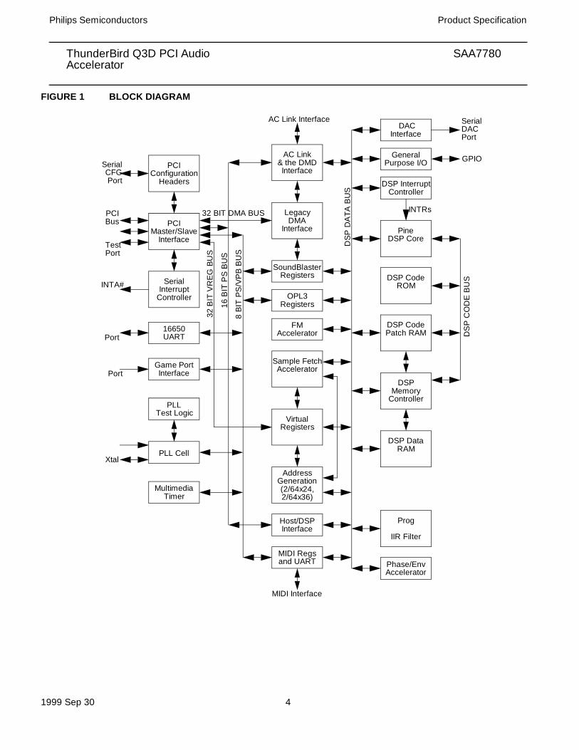
FIGURE 1 BLOCK DIAGRAM
MIDI Interface
DS
P D
ATA
BU
S
DS
P C
OD
E B
US
8 B
IT P
S/V
PB
BU
S
16 B
IT P
S B
US
PCI
GPIO
INTRs32
BIT
VR
EG
BU
S32 BIT DMA BUS
AC Link Interface Serial
Bus
Port
DACPort
PineDSP Core
FMAccelerator
Phase/EnvAccelerator
DACInterface
DSP CodeROM
DSP CodePatch RAM
DSPMemory
Controller
DSP DataRAM
16650UART
VirtualRegisters
AC Link& the DMDInterface
LegacyDMA
Interface
MultimediaTimer
PLLTest Logic
PLL Cell
Game PortInterface
PCIConfiguration
Headers
SerialInterrupt
Controller
PCIMaster/Slave
Interface
MIDI Regsand UART
OPL3Registers
SoundBlasterRegisters
DSP InterruptController
Sample FetchAccelerator
Host/DSPInterface
AddressGeneration(2/64x24,
INTA#
Port
Xtal
Prog
IIR Filter
SerialCFGPort
TestPort
GeneralPurpose I/O
2/64x36)
ThunderBird Q3D PCI Audio SAA7780Accelerator
Philips Semiconductors Product Specification
1999 Sep 30 5
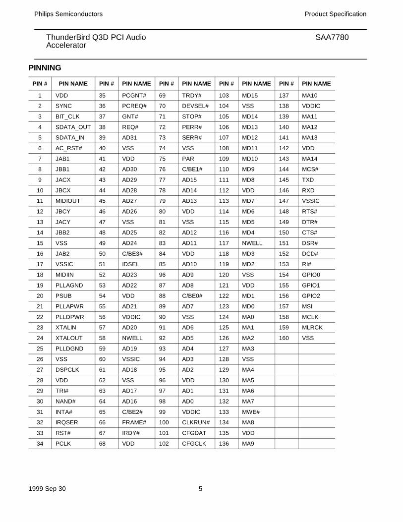
PINNING
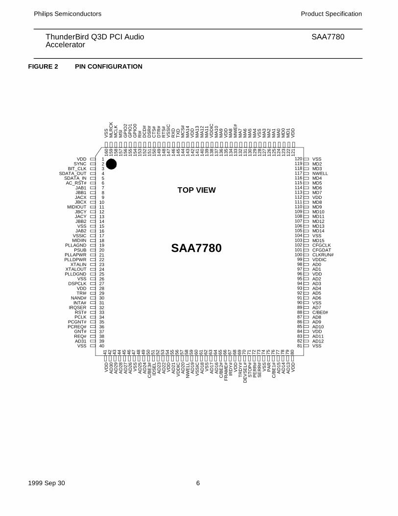
PIN # PIN NAME PIN # PIN NAME PIN # PIN NAME PIN # PIN NAME PIN # PIN NAME
1 VDD 35 PCGNT# 69 TRDY# 103 MD15 137 MA10
2 SYNC 36 PCREQ# 70 DEVSEL# 104 VSS 138 VDDIC
3 BIT_CLK 37 GNT# 71 STOP# 105 MD14 139 MA11
4 SDATA_OUT 38 REQ# 72 PERR# 106 MD13 140 MA12
5 SDATA_IN 39 AD31 73 SERR# 107 MD12 141 MA13
6 AC_RST# 40 VSS 74 VSS 108 MD11 142 VDD
7 JAB1 41 VDD 75 PAR 109 MD10 143 MA14
8 JBB1 42 AD30 76 C/BE1# 110 MD9 144 MCS#
9 JACX 43 AD29 77 AD15 111 MD8 145 TXD
10 JBCX 44 AD28 78 AD14 112 VDD 146 RXD
11 MIDIOUT 45 AD27 79 AD13 113 MD7 147 VSSIC
12 JBCY 46 AD26 80 VDD 114 MD6 148 RTS#
13 JACY 47 VSS 81 VSS 115 MD5 149 DTR#
14 JBB2 48 AD25 82 AD12 116 MD4 150 CTS#
15 VSS 49 AD24 83 AD11 117 NWELL 151 DSR#
16 JAB2 50 C/BE3# 84 VDD 118 MD3 152 DCD#
17 VSSIC 51 IDSEL 85 AD10 119 MD2 153 RI#
18 MIDIIN 52 AD23 96 AD9 120 VSS 154 GPIO0
19 PLLAGND 53 AD22 87 AD8 121 VDD 155 GPIO1
20 PSUB 54 VDD 88 C/BE0# 122 MD1 156 GPIO2
21 PLLAPWR 55 AD21 89 AD7 123 MD0 157 MSI
22 PLLDPWR 56 VDDIC 90 VSS 124 MA0 158 MCLK
23 XTALIN 57 AD20 91 AD6 125 MA1 159 MLRCK
24 XTALOUT 58 NWELL 92 AD5 126 MA2 160 VSS
25 PLLDGND 59 AD19 93 AD4 127 MA3
26 VSS 60 VSSIC 94 AD3 128 VSS
27 DSPCLK 61 AD18 95 AD2 129 MA4
28 VDD 62 VSS 96 VDD 130 MA5
29 TRI# 63 AD17 97 AD1 131 MA6
30 NAND# 64 AD16 98 AD0 132 MA7
31 INTA# 65 C/BE2# 99 VDDIC 133 MWE#
32 IRQSER 66 FRAME# 100 CLKRUN# 134 MA8
33 RST# 67 IRDY# 101 CFGDAT 135 VDD
34 PCLK 68 VDD 102 CFGCLK 136 MA9
ThunderBird Q3D PCI Audio SAA7780Accelerator
Philips Semiconductors Product Specification
1999 Sep 30 6
FIGURE 2 PIN CONFIGURATION
120119118117116115114113112111110109108107106105104103102101100
99989796959493929190898887868584838281
160
159
158
157
156
155
154
153
152
151
150
149
148
147
146
145
144
143
142
141
140
139
138
137
136
135
134
133
132
131
130
129
128
127
126
125
124
123
122
121
123456789
10111213141516171819202122232425262728293031323334353637383940
41 42 43 44 45 46 47 48 49 50 51 52 53 54 55 56 57 58 59 60 61 62 63 64 65 66 67 68 69 70 71 72 73 74 75 76 77 78 79 80
TOP VIEW
SAA7780
VSSMD2MD3NWELLMD4MD5MD6MD7VDDMD8MD9MD10MD11MD12MD13MD14VSSMD15CFGCLKCFGDATCLKRUN#VDDICAD0AD1VDDAD2AD3AD4AD5AD6VSSAD7C/BE0#AD8AD9AD10VDDAD11AD12VSS
VS
SM
LRC
KM
CLK
MS
IG
PIO
2G
PIO
1G
PIO
0R
I#D
CD
#D
SR
#C
TS#
DTR
#R
TS#
VS
SIC
RX
DTX
DM
CS
#M
A14
VD
DM
A13
MA
12M
A11
VD
DIC
MA
10M
A9
VD
DM
A8
MW
E#
MA
7M
A6
MA
5M
A4
VS
SM
A3
MA
2M
A1
MA
0M
D0
MD
1V
DD
VDDSYNC
BIT_CLKSDATA_OUT
SDATA_INAC_RST#
JAB1JBB1JACXJBCX
MIDIOUTJBCYJACYJBB2VSS
JAB2VSSICMIDIIN
PLLAGNDPSUB
PLLAPWRPLLDPWR
XTALINXTALOUTPLLDGND
VSSDSPCLK
VDDTRI#
NAND#INTA#
IRQSERRST#PCLK
PCGNT#PCREQ#
GNT#REQ#AD31VSS
VD
DA
D30
AD
29A
D28
AD
27A
D26
VS
SA
D25
AD
24C
/BE
3#ID
SE
LA
D23
AD
22V
DD
AD
21V
DD
ICA
D20
NW
ELL
AD
19V
SS
ICA
D18
VS
SA
D17
AD
16C
/BE
2#FR
AM
E#
IRD
Y#
VD
DTR
DY
#D
EV
SE
L#S
TOP
#P
ER
R#
SE
RR
#V
SS
PA
RC
/BE
1#A
D15
AD
14A
D13
VD
D
ThunderBird Q3D PCI Audio SAA7780Accelerator
Philips Semiconductors Product Specification
1999 Sep 30 7
FUNCTIONAL OVERVIEW
True Hardware AccelerationThe ThunderBird PCITM products are true hardware accelerators. Positional 3D, music synthesis and SoundBlasterTM functions are performed on the ActiMediaTM DSP which frees the host CPU to perform other tasks, boosting graphic frame rates and raising system benchmark performance.
High ConcurrencyToday's multimedia applications demand concurrent, independent audio processing of many diverse audio streams. Mainstream applications may require 32 or more wavetable synthesis voices and 24 or more sound effects positioned in 3D space concurrently with other audio stream processing. The ThunderBird Q3DTM can simultaneously process 64 combined audio and wavetable voice streams in H/W plus an additional 64 audio streams using QSound's efficient MMX host engine for a total of 128 audio and wavetable streams. For greater concurrency and higher music polyphony a professional quality 256 voice soft-synth is available. This can be used for all music synthesis reserving all 128 streams for other audio sources bringing the total concurrency to 384 streams.
Immersive 3D AudioThe ThunderBird Q3DTM is armed with the most advanced arsenal of 3D technology available. The listener is immersed in a realistic 3 dimensional soundscape. QSound’s technology renders 3D applications using stereo speakers, headphones or quad speakers; and transforms ordinary stereo applications from games to CD players into 3D and quad applications.
QInteractive3DTM (QI3DTM ) utilizes the ActiMedia DSP to interactively position DirectSound streams in 3D space around the listener. Three different 3D engines based on HRTF and patented QSound Technology are used to render over 2 speakers, headphones or quad speakers. Since the unique 2 speaker engine requires no signal cross cancellation, QI3D provides a more robust 3D imaging than ordinary HRTF processing with minimal sensitivity to speaker placement, speaker quality and listener location. QI3D utilizes the industry standard DirectSound3D API and is compatible with DirectSound3D and A3DTM applications.
QSound Environmental ModelingTM (QEMTM) adds further realism by using reverb as an additional positional que. With QEM enabled each DirectSound3D sound source receives reverb simulating acoustic reflections based on the regions reverb preset and the sources current position relative to the listener. Reverb presets can also me manually enabled by the listener for DirectSound3D applications that do not support EAX. QEM is EAXTM 1.0 compatible.
QSound Multi-Speaker SystemTM(QMSSTM) utilizes a proprietary stereo-to-quad remapping algorithm to transform ordinary stereo applications into more immersive quad applications. Unlike some other implementations that simply mirror the front speaker content in the rear speakers QMSS creates 4 individual channels. For musical applications different instruments or sounds will seem to emanate from one or more speakers. For 1st person gaming applications and movie playback, QMSS will estimate approximate placement of each sound based on the stereo mix and adjust it's amplitude and timing in each speaker accordingly.
QMSS can be used to dramatically enhance numerous stereo applications. DirectSound games become more realistic with action all around the listener. Music CD, MP3, and MIDI playback become more immersive. Stereo and Dolby ProLogicTM film clips become the theatre-like in presentation without a decoder required. QMSS can also be used to enhance Dolby Digital DVD playback using only the stereo or Dolby ProLogic audio tracks. Many viewers prefer this alternative to standard Dolby digital playback because of the additional audio content in the rear speakers. QI3D can also be used for more traditional quad playback of Dolby Digital DVD's when combined with a soft-DVD player using the DirectSound3D API.
QXpander enhances 2 speaker playback by broadening the sound field and mapping stereo positions to 3D positions.
ThunderBird Q3D PCI Audio SAA7780Accelerator
Philips Semiconductors Product Specification
1999 Sep 30 8
CD Quality Wavetable Synthesis with 320 Total VoicesThunderBird Q3DTM includes two wavetable synthesis engines. When configured for wavetable synthesis only the ActiMedia DSP can produce up to 64 wavetable 44KHz, 16 bit voices. Using the ActiMedia engine minimizes CPU consumption and is ideal for games with MIDI music tracks. Also available is a professional quality soft-synth that can produce up to 256 voices including special effects. The soft-synth is highly configurable and can be optimized for highest quality with pure music applications or for minimum CPU consumption in gaming applications.
Both engines maximize quality and minimize cost by using system memory for wavetable sample sets and the ActiMedia engine can be used to accelerate DirectMusic and DLS (Down Loadable Sound) sample sets using WDM drivers.
ActiMedia DSP ArchitectureThe ActiMedia architecture combines the strengths of both programmable and fixed function DSP architectures. A programmable DSP processor enables custom features, field up-grade and ease of development. An array of gate-efficient fixed function DSP processors (accelerators) operate in parallel with the programmable DSP, providing an extremely high performance-to-cost ratio. Unlike fixed-point DSP's that must use a single resolution for all audio processing, each accelerator is designed with the optimum resolution for its function. This preserves the audio integrity without the cost of a high-resolution or floating point programmable DSP implementation. The result is a performance, quality and concurrency that requires 10 times the MIPS on a classical DSP architecture.
Digital Mode Dual Game PortThe S/W polling used by analog game ports can consume up to 10% of the host CPU. ThunderBird PCI products utilize a digital operating mode that can eliminate S/W polling and accelerate the game port function resulting in significantly improved system performance. Joystick buttons can be polled or interrupt driven to further enhance performance. A default analog mode assures compatiblitiy with DOS and other non-DirectInputTM applications.
PCI InterfaceThe ThunderBird Q3DTM is a PCI 2.1 compliant multifunction device including audio, game port and 16650 UART functions capable of bursting at 132 MB data rates. The high bandwidth and low latency of the PCI bus reduces the need for host based processing and local memory. The PCI bus consumption of each audio stream is reduced by a factor of 10 compared to ISA solutions. The PCI and CPU busses are no longer locked during slow ISA DMA transactions and system performance is improved as much as 20%.
To maximize performance, the PCI interface includes dual 32 bit bus masters: DMA, DirectSound and wavetable synthesis acceleration. A 16 bit DSP Master Device is used to transfer data directly between the host and DSP or AC97 interface. Additional slave devices support legacy and MIDI interfaces. All I/O is re-mappable creating a true "Plug and Play" device.
Comprehensive Legacy Audio SupportSoundBlaster Pro compatibility in both Real Mode DOS and DOS windows is achieved through H/W SoundBlaster and OPL 3 (FM) emulation registers. Legacy DMA over the PCI bus is supported on all major platforms utilizing PC/PCI, DDMA, or VLSI's proprietary Legacy Accommodation ModeTM (LAMTM). DOS music synthesis includes stereo MIDI playback, quad MIDI playback, and FM emulation.
Integrated I/O and PeripheralsThunderBird Q3D products include all the required features to implement a PCI audio solution with minimal chip count. I/O includes an AC97 link for a AC97 1.0 codec, stereo DAC serial port for multi-channel or low cost playback
ThunderBird Q3D PCI Audio SAA7780Accelerator
Philips Semiconductors Product Specification
1999 Sep 30 9
applications, MPU-401 UART with MIDI IN and MIDI Out connections for external keyboard, sequencer, synthesizer or other MIDI devices, 16650 UART for modem, other serial connections or usage as GPIO's , I2C configuration port for storage of SubSystem/Vendor ID's and other data in serial EEPROM, dual Game Port and 3 GPIO's, and an external SRAM interface for DSP code development or field programmable applications. Only a single 14.318 MHz crystal is required to support the internal PLL. A 20bit, 1us resolution timer is provided for DirectXTM audio/video synchronization.
Operating System SupportVXD driver support includes: WIN95, WIN98, and NT 4.0. WDM driver support will include WIN98 and NT 5.0/WIN2000.
Power ManagementThunderBird Q3D provides localized clock control and full event monitoring including interrupts, I/O and S/W events. Independent power down control of the PLL, DSP, and codec is provided and PCI CLKRUN protocol is supported. Power management h/w hooks exist to achieve compliancy with ACPI and "On Now" initiatives.
ThunderBird Q3D PCI Audio SAA7780Accelerator
Philips Semiconductors Product Specification
1999 Sep 30 10
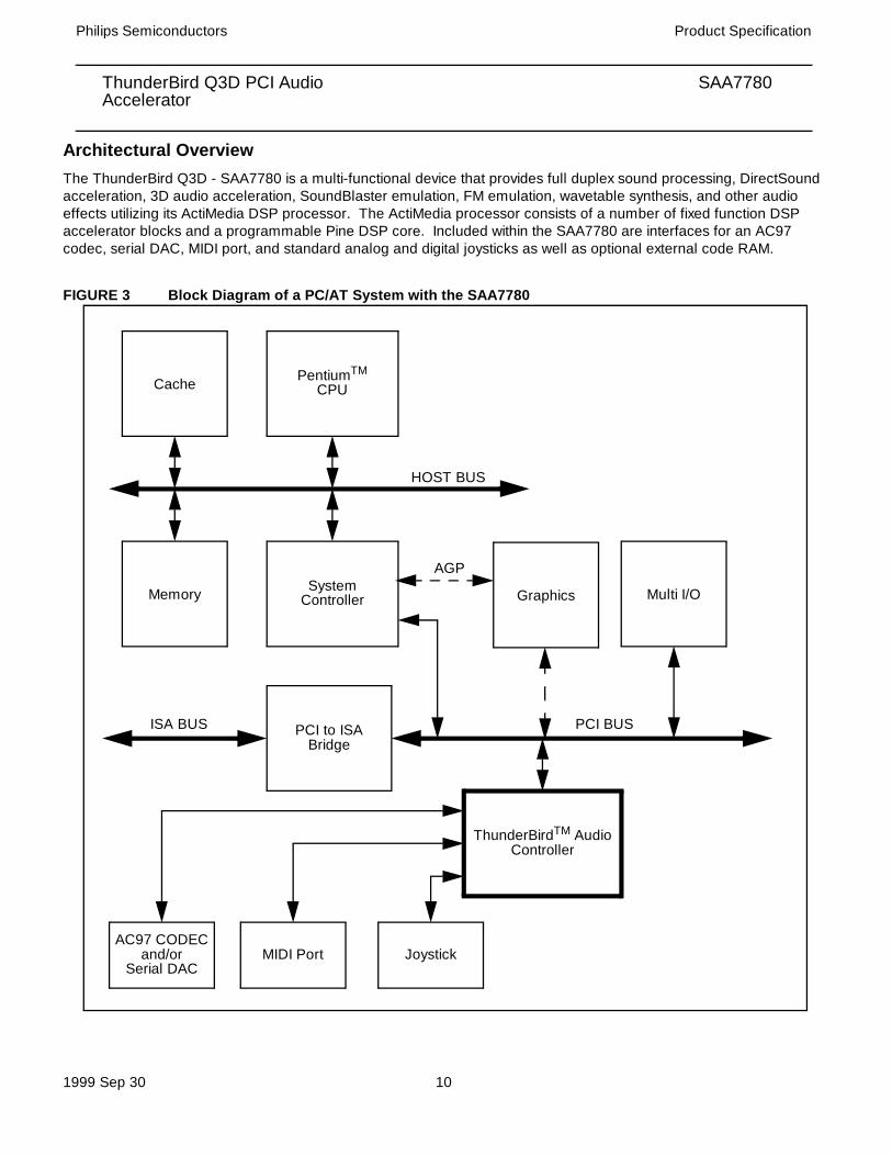
Architectural OverviewThe ThunderBird Q3D - SAA7780 is a multi-functional device that provides full duplex sound processing, DirectSound acceleration, 3D audio acceleration, SoundBlaster emulation, FM emulation, wavetable synthesis, and other audio effects utilizing its ActiMedia DSP processor. The ActiMedia processor consists of a number of fixed function DSP accelerator blocks and a programmable Pine DSP core. Included within the SAA7780 are interfaces for an AC97 codec, serial DAC, MIDI port, and standard analog and digital joysticks as well as optional external code RAM.
FIGURE 3 Block Diagram of a PC/AT System with the SAA7780
SystemController
Cache
PCI to ISABridge
ThunderBirdTM AudioController
Graphics Multi I/O
PentiumTM
CPU
Memory
HOST BUS
ISA BUS PCI BUS
AC97 CODECand/or
Serial DACJoystickMIDI Port
AGP
ThunderBird Q3D PCI Audio SAA7780Accelerator
Philips Semiconductors Product Specification
1999 Sep 30 11
Systems that provide DDMA or have the ISA bridge on the primary PCI bus are able to perform SoundBlaster emulation enabling the operation of legacy DOS based games. The SAA7780 chip provides two 8237 style DMA channels to perform legacy DMA cycles on selected systems. The same two 8237 channels provide Distributed DMA support as well. PC/PCI is also supported to provide legacy DMA support on chipsets that support said protocol.
DirectSound acceleration, both for 2D and 3D audio along with wavetable sample fetching, is accomplished using the SAA7780 chip PCI 2.1 bus master. This bus master provides the means for the SAA7780 chip to accelerate DirectSound audio streams as well as fetch wavetable samples for the 64 voice wavetable synthesis and effects algorithms. Wavetable sample fetching is always retrieved from system memory saving the cost of an external wavetable ROM. Downloadable sample sets, with software, are also supported using the bus master hardware.
Additionally, the SAA7780 chip follows the AC97 Architecture to provide high quality audio by the use of a separate codec. Serial DACs, as well as an AC97 CODEC can be selected to provide audio into the analog world. A serial DAC is used in case the system designer wishes to use an inexpensive playback converter and does not require a record function. A codec and a DAC can be used if multi-channel audio is required.
The SAA7780 chip supports additional interfaces to sustain both required and optional features. These interfaces include a standard 4-axis/4 button joystick, external MIDI port, an SRAM interface for external DSP code or enhanced reverb, and a 16650 UART for an external modem.
The ActiMedia DSP runs the audio algorithms for wavetable synthesis, FM synthesis, special effects such as reverb and chorus, along with sample rate conversion and data management. The imbedded DSP core and its peripherals are managed solely by the DSP and require no intervention from the host. The DSP can pass messages to and from each domain to provide a host software interface into the DSP domain.
Structural and Functional OverviewThe SAA7780 contains components to implement the sound generation with accessories to add value to a gaming type environment. In short, there are three basic types of blocks to implement all of the advanced features present in this chip. The three types of blocks are PCI domain, DSP domain and mailbox. The PCI domain type of blocks refer to the blocks that connect only to the internal and external PCI interfaces. The DSP domain blocks connected only to the DSP code or data busses. The mailbox type interfaces between both worlds providing both functional and test operations between the two domains. The following sections will give more details on the function and operation of each block.
PCI Interface, Configuration and Interrupt SerializerThe SAA7780 chip PCI interface is composed of master and slave state machines, an address/data/byte enable datapath, a bus arbiter for the two on chip masters, control logic for the master and slave internal busses, an interrupt serializer, and the standard PCI configuration register header.
The standard PCI configuration header is also supported. Since the SAA7780 is a multi-function device, there are three PCI configuration spaces allocated for each function. The three functions are the audio device, the joystick and the 16650 UART. The purpose of the multiple configuration headers is to ensure PCI compliance and enable the operating system to select the correct software driver for each individual device. The Serial CFG Port is used to shift in subvendor specific data for each of the PCI configuration headers. The Serial CFG port is an industry standard I2CTM format. The configuration headers are included in the PCI interface to reduce inter-block routing. All other PCI configuration space registers are included in the blocks that utilize these registers.
16650 UARTIn order to support an external hardware modem chip set, a 16650 UART is included in the SAA7780 chip. The 16650 UART excludes the need for an additional ISA based UART thereby reducing system costs. The 16650 UART resides in I/O space and is re-mappable.
ThunderBird Q3D PCI Audio SAA7780Accelerator
Philips Semiconductors Product Specification
1999 Sep 30 12
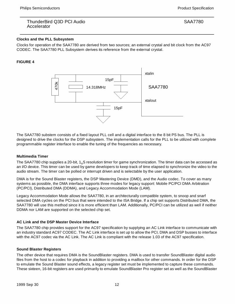
Clocks and the PLL SubsystemClocks for operation of the SAA7780 are derived from two sources; an external crystal and bit clock from the AC97 CODEC. The SAA7780 PLL Subsystem derives its reference from the external crystal.
FIGURE 4
The SAA7780 substem consists of a fixed layout PLL cell and a digital interface to the 8 bit PS bus. The PLL is designed to drive the clocks for the DSP subsystem. The implementation calls for the PLL to be utilized with complete programmable register interface to enable the tuning of the frequencies as necessary.
Multimedia TimerThe SAA7780 chip supplies a 20-bit, 1uS resolution timer for game synchronization. The timer data can be accessed as an I/O device. This timer can be used by game developers to keep track of time elapsed to synchronize the video to the audio stream. The timer can be polled or interrupt driven and is selectable by the user application.
DMA is for the Sound Blaster registers, the DSP Mastering Device (DMD), and the Audio codec. To cover as many systems as possible, the DMA interface supports three modes for legacy support: Mobile PC/PCI DMA Arbitration (PC/PCI), Distributed DMA (DDMA), and Legacy Accommodation Mode (LAM).
Legacy Accommodation Mode allows the SAA7780, in an architecturally compatible system, to snoop and snarf selected DMA cycles on the PCI bus that were intended to the ISA Bridge. If a chip set supports Distributed DMA, the SAA7780 will use this method since it is more efficient than LAM. Additionally, PC/PCI can be utilized as well if neither DDMA nor LAM are supported on the selected chip set.
AC Link and the DSP Master Device InterfaceThe SAA7780 chip provides support for the AC97 specification by supplying an AC Link interface to communicate with an industry standard AC97 CODEC. The AC Link interface is set up to allow the PCI, DMA and DSP busses to interface with the AC97 codec via the AC Link. The AC Link is compliant with the release 1.03 of the AC97 specification.
Sound Blaster Registers The other device that requires DMA is the SoundBlaster registers. DMA is used to transfer SoundBlaster digital audio files from the host to a codec for playback in addition to providing a mailbox for other commands. In order for the DSP to emulate the Sound Blaster sound effects, a legacy register set must be implemented to capture these commands. These sixteen, 16-bit registers are used primarily to emulate SoundBlaster Pro register set as well as the SoundBlaster
xtalin
xtalout
SAA7780
15pF
15pF
14.318MHz470k
ThunderBird Q3D PCI Audio SAA7780Accelerator
Philips Semiconductors Product Specification
1999 Sep 30 13
Pro mixer registers. These registers are used as a mailbox to the DSP data bus to deliver data to the SoundBlaster Emulation code. The SAA7780 chip supports DMA to the Sound Blaster that legacy code requires. All data transmitted over the SoundBlaster Registers is processed by the DSP to emulate the Sound Blaster Pro hardware.
OPL3 Registers and the FM Accelerator The OPL3 register interface is a subset of the complete SoundBlaster register set. The OPL3 registers are separate to point out that the FM legacy is supported at the register level. The OPL3 registers simply pass FM synthesis commands to the SoundBlaster Emulation code and receive status from the same code.
Virtual RegistersThe Virtual Registers interfaces the PCI bus and two substantial wavetable synthesis accelerators: the Sample Fetch and Address Generation accelerators. The Virtual Registers is responsible for setting up the PCI interface for master cycles data fetches and retrieving those fetches into a sample buffer. The Virtual Registers get commands from the Address Generation accelerator and turns them into PCI master requests. Once the data has been retrieved, the Virtual Register then instructs the Sample Fetch accelerator to process a block of data. Once the processing is complete, the Sample Fetch Accelerator notifies the Virtual Registers that all is clear and that new data can be processed.
Address Generation Accelerator The Address Generation accelerator is a preprocessing unit for the sample fetching mechanism inside the Virtual Registers. The Address Generator will get a set of parameters from the DSP code on a per voice basis for either DirectSound processing or wavetable synthesis. Once these voice parameters are set, the hardware is instructed to translate the addresses and fetch the audio samples from system memory. The Address Generator is also capable of looping with intervention from the DSP code. The DSP kills voices by instructing the Address Generator to stop fetching data. Once the samples are fetched, they are stored in the Virtual Register’s input sample buffer for processing by the Sample Fetch Accelerator.
Sample Fetch AcceleratorThe Sample Fetch accelerator is used to process audio samples fetched by the Virtual Registers and deliver them to the DSP code for further processing. This processing can include pitch shifting or rate conversion. The degree of pitch shifting is under direction of DSP code indicating the Sample Fetch accelerator is programmable. The input samples are taken from the Virtual Register’s input sample buffer and stored in DSP memory space.
MIDI Registers and UARTAn MPU401 compatible UART is supplied to enable external MIDI devices to use the SAA7780 chip synthesizers as well as its external device’s own synthesizer. The MIDI register interface is used to pass the MIDI command stream from the host to the DSP firmware for parsing into synthesizer commands. The MPU401 UART always operates in “dumb” mode. Both the PCI and DSP can access the MIDI UART directly. Data is presented from/to the MPU401 Registers in a mailbox fashion to the MPU401 UART.
Music DAC InterfaceThe music DAC interface allows for an inexpensive, high quality, playback of the final stereo mix or for providing the unique QUAD feature when used in conjunction with the standard AC97 V1.03 CODEC. The interface is a standard EIAJ format supporting many brands of inexpensive 16 bit DACs. The Music DAC interface is capable of playback sample rates from 22.05 - 48.0 KHz.
ThunderBird Q3D PCI Audio SAA7780Accelerator
Philips Semiconductors Product Specification
1999 Sep 30 14
General Purpose Input/Output There are five general purpose I/O pins that are controlled by the DSP. These pins can be used for power management of external devices or for test and debug of DSP code. All are full time available under DSP code control. These GPIOs are not controllable from the PCI bus and are generally not available to users.
PINE DSP CoreThe Pine DSP core is a programmable 16-bit integer DSP with separate code and data busses (Harvard architecture). Main features of the DSP core include 2K x 16 data RAM, 64K word code and data space, 16 x 16 bit two’s complement parallel multiplier with 32-bit product, single cycle multiply/accumulate instructions, 36-bit ALU, two 36-bit accumulators, six-general purpose 16-bit pointer registers, option for up to eight user-defined 16-bit registers, zero overhead looping, repeat and block-repeat instructions with one nesting level, shifting capability, automatic saturation mode on overflow while reading content of accumulators, divide and normalize step support.
As noted on Figure 1, the DSP subsystem is supported by two dedicated Pine internal busses called the DSP code bus and the DSP data bus. All DSP peripherals are connected to the DSP data bus while the code bus is used for just that, DSP code ROM and RAM. Both the DSP code and data busses are 16-bit for the address and data lines on each bus. DSP code also enables the DSP core to act as a PCI bus master making it a powerful and flexible audio processing unit.
DSP Interrupt Controller The DSP Interrupt Controller is a programmable, priority encoded device that encodes two interrupt signals to the Pine core. The DSP Interrupt Controller resides on the DSP data bus and is programmed by DSP code. Both sets of interrupt vectors feature an enable and status bit for each interrupt based device.
DSP Memory Controller The DSP memory controller provides controls and decodes for the regular DSP data and code RAMs as well as the code ROMs. The Memory Controller also includes a patch mechanism to allow ROM code to be updated or fixed using a trapping device.
Game PortThe SAA7780 Game Port interface is designed to emulate the PC-AT based legacy joystick operation as well as support of a digital joystick mode. The legacy or analog, type of operation is designed to support all legacy software that uses the original joystick address and the method for resolving the joystick axes positions. The Digital Mode is designed to reduce the joystick overhead by resolving the joystick position directly and to support applications that use DirectInput.
The legacy joystick used a one shot multi-vibrator on each of the four joystick potentiometers. These one shots were set up to deliver a pulse that was proportional to the resistor value of the joystick potentiometers. Software would them poll the one shots to see if they had been set to the original value. The time it took for each axes to return to the original value was resolved into a position by the legacy software. The SAA7780 emulates the 558 based one shot circuit to support legacy games that use the PC-AT joystick. The joystick button values were routed directly to the system bus where only a decode was required to read the value of the button. Software would poll the buttons as well. All button and joystick axes data is returned in a single byte wide register.
Game Port Legacy I/O Register This register is the legacy mode register for the 558 based joystick. Typically, this register is located at legacy address of 201h. Reads from this register will poll the status of the joystick buttons and are used to resolve the position. Writes
ThunderBird Q3D PCI Audio SAA7780Accelerator
Philips Semiconductors Product Specification
1999 Sep 30 15
to this register will discharge the external capacitors to emulate the 558 one shots. Software can then poll the joystick register bit to resolve each of the joystick axes positions by timing. The joystick button register bits have meaning in both the digital and analog modes. The axes bits are only valid for analog mode.
Game Port 558-Based Register - Gameport (RO) )
SAA7780 Signal Definitions
PCI Local Bus Interface Signals
I/O GMBASE D7 D6 D5 D4 D3 D2 D1 D0
Offset 1h JOYB_2 JOYB_1 JOYA_2 JOYA_1 JOYB_Y JOYB_X JOYA_Y JOYA_X
POR Value 1 1 1 1 0 0 0 0
Bit Name R/W Function
7 JOYB_2 RO Joystick B button 2 status. The joystick buttons should be de-bounced and de-glitched from the chip interface. The joystick button status registers are cleared when the joystick button is pressed.
6 JOYB_1 RO Joystick B button 1 status.
5 JOYA_2 RO Joystick A button 2 status.
4 JOYA_1 RO Joystick A button 1 status.
3 JOYB_Y RO Joystick B y-coordinate. Can also be referred to as position 3.
2 JOYB_X RO Joystick B x-coordinate. Can also be referred to as position 2.
1 JOYA_Y RO Joystick A y-coordinate. Can also be referred to as position 1.
0 JOYA_X RO Joystick A x-coordinate. Can also be referred to as position 0.
AD[31:0] 39,42,43,44,45,46,48,49,52,53,55,57,59,61,63,64,77,78,79,82,83,85,86,87,89,91,92,93,94,95,97,98
IO-T PCI Address/Data
AD[31:0] contains a physical byte address during the first clock of a PCI transaction, and data during subsequent clocks.
When the SAA7780 is a PCI master, AD[31:0] are outputs during the address phase of a transaction. They are either inputs or outputs during the data phase, depending on the type of PCI cycle in process.
When the SAA7780 is a PCI slave, AD[31:0] are inputs during the address phase. They are either inputs or outputs during the data phase, depending on the type of PCI cycle in process.
ThunderBird Q3D PCI Audio SAA7780Accelerator
Philips Semiconductors Product Specification
1999 Sep 30 16
C/BE#[3:0] 50,65,76,88 IO-T PCI Bus Command and Byte Enables
C/BE#[3:0] defines the bus command during the first clock of a PCI transaction, and the byte enables during subsequent clocks.
C/BE#[3:0] are outputs when the SAA7780 is a PCI bus master and inputs when it is a PCI bus slave.
DEVSEL# 70 IO-STS PCI Bus Device Select
When the SAA7780 is a PCI bus master the SAA7780 uses DEVSEL# to determine whether a master abort should occur if DEVSEL# is not sampled active by clock 5 of the transaction, or to determine whether a cycle is to be aborted or retried when a target-initiated termination occurs.
When the SAA7780 is a PCI bus slave, DEVSEL# is an output which the SAA7780 drives LOW during the second PCLK after FRAME# assertion to the end of a transaction if the SAA7780 is selected.
FRAME# 66 IO-STS PCI Bus Cycle Frame
When the SAA7780 is a PCI master, FRAME# is an output which indicates the beginning of a SAA7780-initiated bus transaction. While FRAME# is asserted data transfers continue. When FRAME# is deasserted the transaction is in the final data phase.
When the SAA7780 is a PCI slave, FRAME# is an input that initiates an I/O, memory or configuration register access if the SAA7780 is selected for the transaction. The SAA7780 latches the C/BE#[3:0] and AD[31:0] signals on the PCLK edge on which it first samples FRAME# active.
IRDY# 67 IO-STS PCI Bus Initiator Ready
When the SAA7780 is a PCI master, IRDY# is an output which indicates the SAA7780’s ability to complete the data phase of the current transaction. It is always asserted from the PCLK cycle after FRAME# is asserted to the last clock of the transaction.
When the SAA7780 is a PCI slave, IRDY# is an input which causes the SAA7780 to hold-off completion of a read or write cycle until sampled active.
STOP# 71 IO-STS PCI Bus Stop (Target Initiated Termination)
When the SAA7780 is a PCI master, STOP# is an input which causes the SAA7780 to complete, abort or retry the transfer, depending on the state of TRDY# and DEVSEL#.
When the SAA7780 is a PCI slave, it drives STOP# as active (LOW) to terminate or retry a transaction.

ThunderBird Q3D PCI Audio SAA7780Accelerator
Philips Semiconductors Product Specification
1999 Sep 30 17
TRDY# 69 IO-STS PCI Bus Target Ready
When the SAA7780 is a PCI master, TRDY# is an input which indicates the target agent’s ability to complete the data phase of the transaction. After initiation of a PCI bus transaction, the SAA7780 inserts wait cycles until TRDY# is sampled active.
When the SAA7780 is a PCI slave, it drives TRDY# active to indicate that the SAA7780 has sampled the data from AD[31:0] during a write phase, or presented valid data on AD[31:0] during a read phase.
PAR 75 IO-T PCI Bus Parity
When the SAA7780 is a PCI master, it drives PAR to reflect the correct value for even parity on the AD[31:0] and C/BE#[3:0] buses one clock after the address phase and after each write data phases.
When the SAA7780 is a PCI slave, it drives PAR to reflect the correct value for even parity on the AD[31:0] and C/BE#[3:0] buses one clock after completion of each read data phase.
PCREQ# 36 O-TS PC/PCI DMA Request
This signal requests DMA servies from en external chipset that supports PC/PCI protocols. The SAA7780 chip asserts PCGNT# according to the desired DMA channel required by either the SoundBlaster or AC97 interfaces. The requested channel is encoded serially on the PCGNT# pin.
The SAA7780 will become the bus owner when it receives an asserted PCGNT# signal. This handshaking is synchronous to PCLK.
PCGNT# 35 I-T PC/PCI DMA Grant
An asserted PCGNT# pin indicates that the external PC/PCI master arbiter has granted DMA services to the the encoded DMA channel to the requesting DMA agent on the SAA7780 chip.
REQ# 38 O-TS PCI Bus Request
This signal controls the PCI bus arbitration between the SAA7780 chip and the PCI master arbiter. When REQ# is asserted, the SAA7780 indicates a desire to become the PCI bus owner. The SAA7780 will become the bus owner when it receives an asserted grant signals (GNT# is LOW). This handshaking is synchronous to PCLK.
REQ# is three-stated while RST# is active.
ThunderBird Q3D PCI Audio SAA7780Accelerator
Philips Semiconductors Product Specification
1999 Sep 30 18
GNT# 37 I-T PCI Bus Grant
An asserted GNT# pin indicates that the PCI master arbiter has granted bus ownership to the SAA7780 chip.
IRQSER 32 IO-OD PCI Bus Serial Interrupts
This pin is used to output the serial interrupt stream for legacy interrupts. It is used only if the SAA7780 is used in a Common Architecture system. Otherwise it is tri-stated.
INTA# 31 IO-OD PCI Bus Interrupt A
The interrupt output is a PCI compatible active low level sensitive interrupt. It is only used if the SAA7780 is used in a non Common Architecture system. Otherwise it is tri-stated. It is driven low when any of the internal interrupts are asserted.
PERR# 72 IO-STS PCI Bus Parity Error
This signal indicates a data parity error for any cycle type other than a Special Cycle command. PERR# is made active two clocks after the completion of the data phase which caused the parity error. This error signal may result in the generation of a non-maskable interrupt (NMI) or other high priority interrupt sent to the CPU.
SERR# 73 IO-OD PCI Bus System Error
This signal indicates an address parity error, data parity errors on Special Cycle commands or any other catastrophic system error. SERR# is an open-drain bidirectional pin which is driven low for a single PCLK cycle by the agent reporting the error. This error may result in the generation of a non-maskable interrupt (NMI) or other high priority interrupt sent to the CPU.
IDSEL 51 I-T Initialization Device Select
IDSEL is used as a chip select during configuration register read and write operations. One system board address line from AD[31:11] is used as IDSEL to select the SAA7780 configuration space in the SAA7780 chip when used on the PCI bus.
CLKRUN# 100 O-OD PCI Bus Clock Run Request
The SAA7780 uses CLKRUN# according to the Mobile PCI protocol to start the PCI clock or keep the clock running whenever an internal PCI device requires it.
ThunderBird Q3D PCI Audio SAA7780Accelerator
Philips Semiconductors Product Specification
1999 Sep 30 19
Serial Configuration Port
Test Interface
PCLK 34 I-T PCI Bus Clock Input
PCLK is the PCI bus clock input. It is used to synchronize all PCI bus operations and typically runs at 33MHz.
RST# 33 I PCI Bus Reset
An active low version of the system reset, this signal causes the PCI interface to return to the idle states in all state machines and asynchronously three-states all PCI bus signals. All registers will be reset to their default values as well. The CODEC interface line should be all driven inactive along with the external memory interface. This reset will assert the DSP reset.
CFGDAT 101 I,PU-T Serial Configuration Data
This pin is used to shift in PCI configuration data for the Subsystem ID and the Subsystem Vendor ID in each of the PCI configuration headers present in the SAA7780 chip. The Serial Configuration Port is a standard I2C interface. This line should never be pulled low.
CFGCLK 102 O-T Serial Configuration Clock
The serial clock is a 400 KHz clock generated from OSC and supplied to an external serial EEPROM to synchronize the serial configuration data.
TRI# 29 I-T Tri-State Test Enable
When this pin is pulled low and RST# is pulsed asserted, all output and I/O pins of the SAA7780 will be forced into a three-state condition. Pulsed assertion of the RST# signal will release the SAA7780 from this test mode.
NAND# 30 I-T NAND Tree Test Enable
When this pin is pulled low and RST# is pulsed asserted, the SAA7780 will enter the parametric NAND tree test mode. The details of the NAND tree test mode are described later in this document.

ThunderBird Q3D PCI Audio SAA7780Accelerator
Philips Semiconductors Product Specification
1999 Sep 30 20
16650 UART Interface
RXD 146 I-T UART Serial Data Input
This pin provides the serial bit stream to the 550-compatible UART. This input is ignored when the Loop Mode is enabled.
TXD 145 O-T UART Serial Data Output
This pin is an output from UART, providing the serial bit stream to external buffers or devices. This signal is forced high whenever the transmitter is disabled, RST# is asserted, the transmit register is empty, or the UART is in the Loop Mode.
RTS# 148 O-T UART Request To Send
An active low output that is the inverted value of the Modem Control Register (MCR) bit 1, as follows:
When MCR[1] = 1, RTS# is low.
When MCR[1] = 0, RTS# is high.
When RST# is asserted, RTS# is forced high.
DTR# 149 O-T UART Data Terminal Ready
An active low output that is the inverted value of the Modem Control Register bit 0, as follows:
When MCR[0] = 1, DTR# is low.
When MCR[0] = 0, DTR# is high.
When RST# is asserted, DTR# is forced high.
CTS# 150 I-T UART Clear To Send
The status of this input can be determined by reading bit 4 of the Modem Status Register. When MSR[4] is read, it will be the inverted value of CTS#. A change in status of CTS# sets the Delta CTS bit in the Modem Status Register.
If the CTS# line changes state while the modem status interrupts are enabled, an interrupt packet will be generated.
DSR# 151 I-T UART Data Set Ready
The status of this input can be determined by reading bit 5 of the Modem Status Register. When MSR[5] is read, it will be the inverted value of DSR#. A change in status of DSR# sets the Delta DSR bit in the Modem Status Register.
If the DSR# line changes state while the modem status interrupts are enabled, an interrupt will be generated.
ThunderBird Q3D PCI Audio SAA7780Accelerator
Philips Semiconductors Product Specification
1999 Sep 30 21
Joystick/Game Port
DCD# 152 I-T UART Data Carrier Detect
The status of this input can be determined by reading bit 7 of the Modem Status Register. When MSR[7] is read, it will be the inverted value of DCD#. A change in status of DCD# sets the Delta DCD bit in the Modem Status Register.
If the DCD# line changes state while the modem status interrupts are enabled, an interrupt will be generated.
RI# 153 I-T UART Ring Indicator
The status of this input can be determined by reading bit 6 of the Modem Status Register. When MSR[6] is read, it will be the inverted value of RI#. Bit 2 (TERI) of the Modem Status Register indicates whether the RI# input signal has changed from a low to a high, since the previous reading of the Modem Status Register.
If modem status interrupts are enabled when MSR[6] changes from a 1 to a 0, an interrupt will be generated.
JACX 9 I/O-C,S Joystick A X Axis
Joystick A X-position.
JACY 13 I/O-C,S Joystick A Y Axis
Joystick A Y-position.
JBCX 10 I/O-C,S Joystick B X Axis
Joystick B X-position.
JBCY 12 I/O-C,S Joystick B Y Axis
Joystick B Y-position.
JAB[2:1] 7 I-T Joystick A Button Interface
Joystick A buttons. These buttons are internally de-bounced and de-glitched using a low speed clock and metastable hardened flip-flops.
JBB[2:1] 14 I-T Joystick B Button Interface
Joystick B buttons. These buttons are internally de-bounced and de-glitched using a low speed clock and metastable hardened flip-flops.
ThunderBird Q3D PCI Audio SAA7780Accelerator
Philips Semiconductors Product Specification
1999 Sep 30 22
MIDI Interface
PLL/DSP CLK Subsystem Interface
DSP External Memory Interface
MIDIIN 18 I-T MIDI Serial Data Input
This signal is part of the standard 2 wire MIDI interface. This input receives MIDI data at a rate of 31.25Kbaud. Optical isolation is required.
MIDIOUT 11 O-T MIDI Serial Data Output
This signal is part of the standard 2 wire MIDI interface. This output transmits MIDI data at a rate of 31.25Kbaud. Optical isolation is required.
XTALIN
XTALOUT
23
24
I-C
O-C
OSC Clock Crystal Pad
This pin pair describes the pad required for the 14.31818MHz OSC pad oscillator. The OSC clock is used to provide a fixed timebase for many functions within the SAA7780 device.
DSPCLK 27 I-T DSP Clock Input
This pin can be used as the clock input for the SAA7780 for the DSP subsystem in place of the PLL driving the clock. DSPCLK is also used to drive the DSP subsystem for controllability during testing.
PSUB 20 AGND PLL Substrate
PLLDPWR 22 DPWR PLL Digital Power
PLLDGND 25 DGND PLL Digital Ground
PLLAPWR 21 APWR PLL Analog Power
PLLAGND 19 AGND PLL Analog Ground
MA[14:0] 143,141,140,139,137,136,134,132,131,130,129,127,126,125,124
O-T External Memory Address
Address lines for the external SRAM devices. The external memory interface can be used for DSP code space if the EXT_SRAM_EN (in HDCFG, bit 5) is set. Otherwise, the reverb accelerator will use the external SRAM.
ThunderBird Q3D PCI Audio SAA7780Accelerator
Philips Semiconductors Product Specification
1999 Sep 30 23
AC’97 CODEC Interface
MD[15:0] 103,105,106,107,108,109,110,111,113,114,115,116,118,119,122,123
IO-T External Memory Data Bus
Word wide data bus for the external SRAM. Use 6ns memory for DSP code usage and 20 ns memory for reverb usage.
MCS# 144 O-T External Memory Chip Select
Chip select line for the external SRAM devices.
MWE# 133 O-T External Memory Read/Write Control
Selects the external SRAM for reading or writing.
SYNC 2 O-T AC’97 Codec Synchronization/Frame Output
This signal is used to frame the tag packet from the AC link designer from the SAA7780 chip.
BIT_CLK 3 I AC’97 Data Bit Clock
This signal is used to clock synchronous data on the AC link interface.
SDATA_OUT 4 O-T AC’97 Serial Data Out
This is the time division multiplexed serial output data stream from the SAA7780 controller.
SDATA_IN 5 I AC’97 Serial Data In
This is the time division multiplexed serial input data stream the external AC’97 codec.
AC_RST_N# 6 O-T AC’97 Master Reset
The external AC’97 codec has a master reset line which is has a separate control. The codec status must report a ready before any audio or modem data is transmitted to the codec.
ThunderBird Q3D PCI Audio SAA7780Accelerator
Philips Semiconductors Product Specification
1999 Sep 30 24
Music DAC Interface
General Purpose Input/Output
Power and Ground Pins
MSI 157 IO-T Music DAC Serial Data Output
This signal is the serial bit stream used to transmit PCM data to a industry standard serial DAC. Any mono or stereo PCM audio stream can be played from the DSP to this interface to provide music without the need for an AC’97 codec.
If the serial port is disabled, then this pin can be used for general purpose I/O control.
MCLK 158 IO-T Music DAC Data Bit Clock
The MSI data is synchronized to this clock used by an external Music DAC.
If the serial port is disabled, then this pin can be used for general purpose I/O control.
MLRCK 159 IO-T Music DAC Data Word Clock
This signal is used to frame the left and right channel PCM data being transmitted to the external Music DAC.
If the serial port is disabled, then this pin can be used for general purpose I/O control.
GPIO0 154 I/O-T General Purpose I/O Bit 0
This pin can be used for general purpose I/O control.
GPIO1 155 I/O-T General Purpose I/O Bit 1
This pin can be used for general purpose I/O control.
GPIO2 156 I/O-T General Purpose I/O Bit 2
This pin can be used for general purpose I/O control.
VDDIC 138,99 DPWR Core Power
VSSIC 60,147 DGND Core Ground
VSS 26,15,40,47,62,74,81,90,104,120,128,160
DGND Ring Ground
ThunderBird Q3D PCI Audio SAA7780Accelerator
Philips Semiconductors Product Specification
1999 Sep 30 25
Legend: C CMOS-compatible inputAGND Analog groundDGND Digital ground pinI Input-only pin (can become bidirectional for test mode)IO Bidirectional pinO Output-only pin (can become bidirectional for test mode)APWR Analog power supply pinDPWR Digital power supply pinT TTL-compatible inputPD Indicates a high-impedance with approximately 10 K¾ minimum resistance to VSS (internal pull-down
resistor on pin)PU Indicates a high-impedance with approximately 10 K¾ minimum resistance to VDD (internal pull-up resis-
tor on pin)PUB Inidcates that this pin needs an external pull-up resistor when the chip is installed on a board or tester. A
10K ohm resistor is nominalS Indicates a Schmitt-trigger input with hysteresis for noise immunityTS Three-state pinSTS Sustained three-state output / TTL input (if applicable)OD Open drain padA Analog based I/O. Use a pad with ESD protectionCP Core power. Denotes a pad that supplies power for the core of the chip onlyCG Core ground. Denotes a pad that supplies ground to the core onlyRP Ring power. Denotes a pad that supplies power to the pads onlyRG Ring ground. Denotes a pad that supplies ground to the ring onlyRPD Ring power with option to power core level shifter. Denotes a pad that supplies power to the ring while its
core side connector can optionally supply internal level shiftersRCG Ring/core ground. Denotes a pad that supple a ground connection to the ring and coreHZ High impedance. When in a three state test mode, this pin will be forced into a high impedance stateNT Nand tree. When in a NAND tree test mode, this pin will be included in the parametric NAND tree logicNTO Nand tree output. When in a NAND tree test mode, this pin is the output of the parametric NAND treeFSB Function System Block test. Denotes that his pin is not timing critical and is available for FSB multiplexing
VDD 1,142,28,41,54,68,80,96,112,121,135,142
DPWR Ring Power
VWELL 117 DPWR External N-Well Bias
Tie these pins to 5V for proper 5 volt tolerant operation. The 5V supply must be powered up before the 3V supply. Likewise, the 3V supply must be powered down before the 5V supply.
ThunderBird Q3D PCI Audio SAA7780Accelerator
Philips Semiconductors Product Specification
1999 Sep 30 26
SAA7780 Functional Block Descriptions
Register Table Document Description and Example The next table gives an example of how registers are documented in this specification.
Example Register - Regex (RW/RO)
In the above table example, the EXAMPLE REGISTER text would be a descriptive title for the register that we wish to detail. Following the register description would be a register mnemonic used in register summary tables and the like. In this example the mnemonic is REGEX. Following the mnemonic is the read/write access allowed into this register. If the entire register is readable and writable, then the RW key is assigned. If some bits are read/write while others are read only, then the key will indicate this fact. In the example, this register has both read/write and read only bits. The register memory map location is marked in the table cell marked SPACE. SPACE could be substituted with PCI CFG n (for PCI configuration register space for function n), IOBASE (for an I/O space register with an IOBASE specified in a configuration register), DSP DATA (for DSP data memory mapped registers), MEM MSTR (indicating a PCI master in memory space), and DSP CODE (indicating a DSP code memory mapped register. Just below the SPACE marker is the offset from the base address specified in the SPACE field. The rest of the table should be obvious.
SAA7780 PCI Interface
OverviewThe SAA7780 chip PCI interface is designed to interface the external PCI bus interface to all of the selected devices in the SAA7780 chip. The PCI interface composed of master and slave state machines, an address/data/byte enable datapath, a bus arbiter for the two on chip masters, control logic for the master and slave internal busses, and standard PCI configuration register headers. The Interrupt Serializer will be discussed in a later chapter. This section of the specification will describe the PCI interface in more detail along with design considerations for both the slave, master, and datapath. The configuration header will be discussed in the SAA7780 PCI Configuration Registers section of this specification.
The discussion will begin with the PCI master and target systems. The PCI bus master has the capability to burst double words to/from the two internal bus masters, the Distributed DMA and the Virtual Registers. The full address range is supported for these master devices. Since there are two masters, an arbiter is required to determine priority between the two devices. Details on the arbiter can be found in the PCI master section.
SPACE D15 D14 D13 D12 D11 D10 D9 D8
Offset nnh R R R R R R R R
POR Value 0 0 0 0 0 0 0 0
D7 D6 D5 D4 D3 D2 D1 D0
EXDATA[7:0]
POR Value 0 0 0 0 0 0 0 0
Bit Name R/W Function
15:8 R RO Reserved. These bits always return zeros.
7:0 EXDATA RW Example data. The example data for all to see.
ThunderBird Q3D PCI Audio SAA7780Accelerator
Philips Semiconductors Product Specification
1999 Sep 30 27
The PCI datapath block contains the multiplexors and registers to steer the data to and from the PCI interfaces. The data is de-multiplexed from the external PCI interface to the internal master and slave busses. Control logic from the master and slave devices control the datapath.
The SAA7780 is considered a multi-function device since the operating system may wish to load different drivers for certain functions. These functions are the audio subsystem, the joystick and the 16650 UART. Each of these major functions must have a separate PCI configuration space. The standard PCI configuration header for these three functions are supported in the PCI interface.
The SAA7780 PCI interface responds to and initiates PCI cycles with positive decoding according to the PCI 2.1 specification. The interface asserts DEVSEL# after the first clock following FRAME# making it a medium responder. For specific LAM cycles, the SAA7780 will be a fast responder. The following table indicates which cycles the PCI interface responds to or initiates.
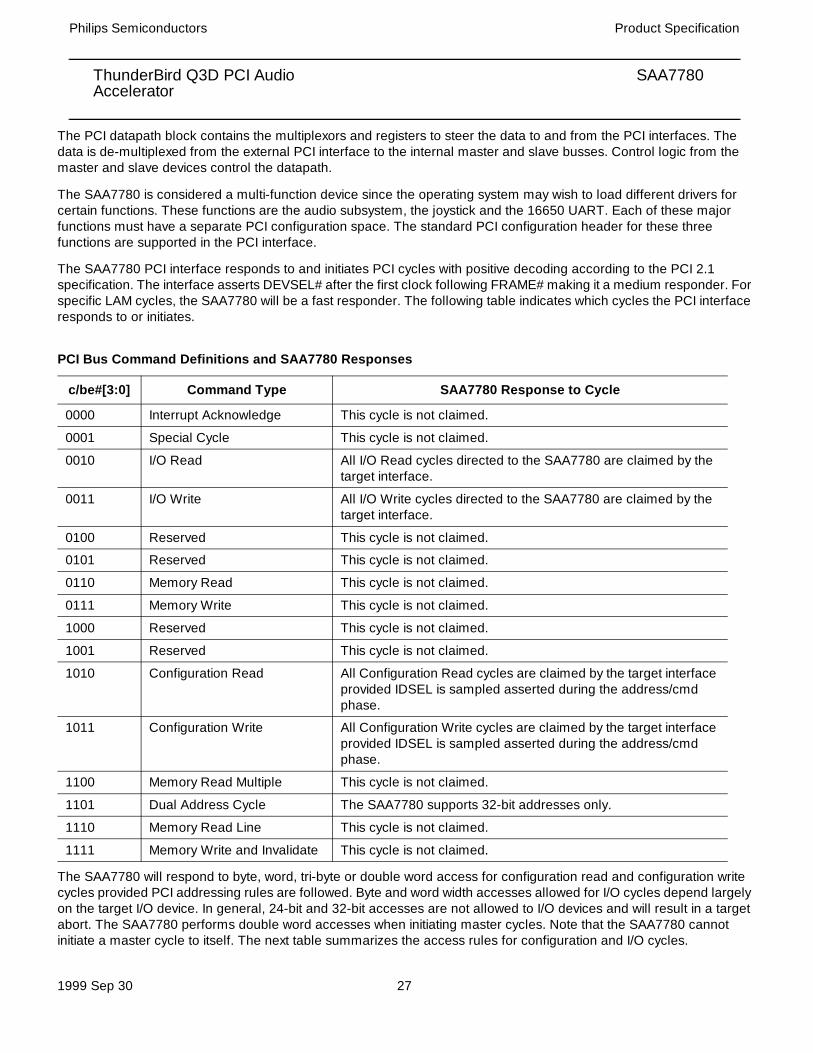
PCI Bus Command Definitions and SAA7780 Responses
The SAA7780 will respond to byte, word, tri-byte or double word access for configuration read and configuration write cycles provided PCI addressing rules are followed. Byte and word width accesses allowed for I/O cycles depend largely on the target I/O device. In general, 24-bit and 32-bit accesses are not allowed to I/O devices and will result in a target abort. The SAA7780 performs double word accesses when initiating master cycles. Note that the SAA7780 cannot initiate a master cycle to itself. The next table summarizes the access rules for configuration and I/O cycles.
c/be#[3:0] Command Type SAA7780 Response to Cycle
0000 Interrupt Acknowledge This cycle is not claimed.
0001 Special Cycle This cycle is not claimed.
0010 I/O Read All I/O Read cycles directed to the SAA7780 are claimed by the target interface.
0011 I/O Write All I/O Write cycles directed to the SAA7780 are claimed by the target interface.
0100 Reserved This cycle is not claimed.
0101 Reserved This cycle is not claimed.
0110 Memory Read This cycle is not claimed.
0111 Memory Write This cycle is not claimed.
1000 Reserved This cycle is not claimed.
1001 Reserved This cycle is not claimed.
1010 Configuration Read All Configuration Read cycles are claimed by the target interface provided IDSEL is sampled asserted during the address/cmd phase.
1011 Configuration Write All Configuration Write cycles are claimed by the target interface provided IDSEL is sampled asserted during the address/cmd phase.
1100 Memory Read Multiple This cycle is not claimed.
1101 Dual Address Cycle The SAA7780 supports 32-bit addresses only.
1110 Memory Read Line This cycle is not claimed.
1111 Memory Write and Invalidate This cycle is not claimed.
ThunderBird Q3D PCI Audio SAA7780Accelerator
Philips Semiconductors Product Specification
1999 Sep 30 28
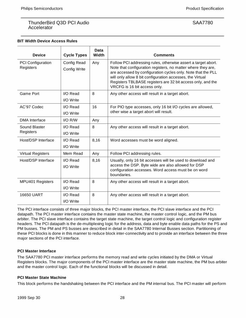
BIT Width Device Access Rules
The PCI interface consists of three major blocks, the PCI master interface, the PCI slave interface and the PCI datapath. The PCI master interface contains the master state machine, the master control logic, and the PM bus arbiter. The PCI slave interface contains the target state machine, the target control logic and configuration register headers. The PCI datapath is the de-multiplexing logic for the address, data and byte enable data paths for the PS and PM busses. The PM and PS busses are described in detail in the SAA7780 Internal Busses section. Partitioning of these PCI blocks is done in this manner to reduce block inter-connectivity and to provide an interface between the three major sections of the PCI interface.
PCI Master InterfaceThe SAA7780 PCI master interface performs the memory read and write cycles initiated by the DMA or Virtual Registers blocks. The major components of the PCI master interface are the master state machine, the PM bus arbiter and the master control logic. Each of the functional blocks will be discussed in detail.
PCI Master State Machine This block performs the handshaking between the PCI interface and the PM internal bus. The PCI master will perform
Device Cycle TypesData
Width Comments
PCI Configuration Registers
Config Read
Config Write
Any Follow PCI addressing rules, otherwise assert a target abort. Note that configuration registers, no matter where they are, are accessed by configuration cycles only. Note that the PLL will only allow 8 bit configuration accesses, the Virtual Registers TBLBASE registers are 32 bit access only, and the VRCFG is 16 bit access only.
Game Port I/O Read
I/O Write
8 Any other access will result in a target abort.
AC’97 Codec I/O Read
I/O Write
16 For PIO type accesses, only 16 bit I/O cycles are allowed, other wise a target abort will result.
DMA Interface I/O R/W Any
Sound Blaster Registers
I/O Read
I/O Write
8 Any other access will result in a target abort.
Host/DSP Interface I/O Read
I/O Write
8,16 Word accesses must be word aligned.
Virtual Registers Mem Read Any Follow PCI addressing rules.
Host/DSP Interface I/O Read
I/O Write
8,16 Usually, only 16 bit accesses will be used to download and access the DSP. Byte wide are also allowed for DSP configuration accesses. Word access must be on word boundaries.
MPU401 Registers I/O Read
I/O Write
8 Any other access will result in a target abort.
16650 UART I/O Read
I/O Write
8 Any other access will result in a target abort.

ThunderBird Q3D PCI Audio SAA7780Accelerator
Philips Semiconductors Product Specification
1999 Sep 30 29
bursting in a linear incrementing type fashion. The PCI master state machine may also wish to provide a target lockout signal. This signal prevents the PCI target interface from responding to any master signals.
PC/PCI Legacy Support The PCI block supports the PC/PCI sideband signals for legacy support of the soundblaster. The PC/PCI can be enabled by a configuration register bit and one channel selected. The PCI slave block will provide the serial encoded request signal (PCREQ#) in response to a request from the soundblaster and decode the serial encoded PCGNT# line. The PCI slave will then claim I/O writes to address 0000h or 0004h with the PCGNT# line asserted as writes to the SoundBlaster and pass the data to the SoundBlaster.
PCI Target State Machine AThe PCI target state machine controls all SAA7780 target responses on the PCI bus in addition to handling the PS internal bus.
PCI Target Control Logic The target control logic handles the address decoding for the ps_NNNcs# signals, bus command decoding for the ps_XXXrd# and ps_XXXwr# signals, determination of target abort conditions, and data path/pad control logic from the target interface. Also included in this logic are the controls for the PCI datapath and I/O pads. These controls are sent to the datapath logic where they are combined with the master controls and then sent to the datapath and pad devices. The control logic also includes an interface to the PCI configuration headers.
Serial Configuration Port The Subsystem Vendor ID and Subsystem ID for each of the configuration headers presents a special case. These three 32 bit registers must be programmed by the Subsystem Vendor. It is impractical to hard wire the Subsystem ID registers since each Subsystem Vendor will have a unique ID. Therefore an external serial EEROM device is used to download the proper values into the ID registers after reset and before begin read by the BIOS or other configuration software. The PCI interface should force a retry if any of the subsystem registers have not completed a loading. The Serial Configuration Port is a standard two pin I2C interface. The SAA7780 will supply the 400 KHz clock to the external serial EEPROM on the CFGCLK pin. The serial data stream will arrive on the CFGDAT input pin. Please refer to a 24LC00 128 bit I2C Bus Serial EEPROM data sheet for interface protocols and timings.
Serial Configuration Port Programming The SAA7780 uses an inexpensive external EEPROM, programmed before installation, to download the Subsystem Vendor ID and Subsystem ID registers for each function for a total of 96 bits (six 16 bit registers). The recommended device, a Microchip 24LC01B 1K Bit (128 Byte) Serial EEPROM, can be programmed using a conventional DATA I/O programmer.
ThunderBird Q3D PCI Audio SAA7780Accelerator
Philips Semiconductors Product Specification
1999 Sep 30 30
FIGURE 5
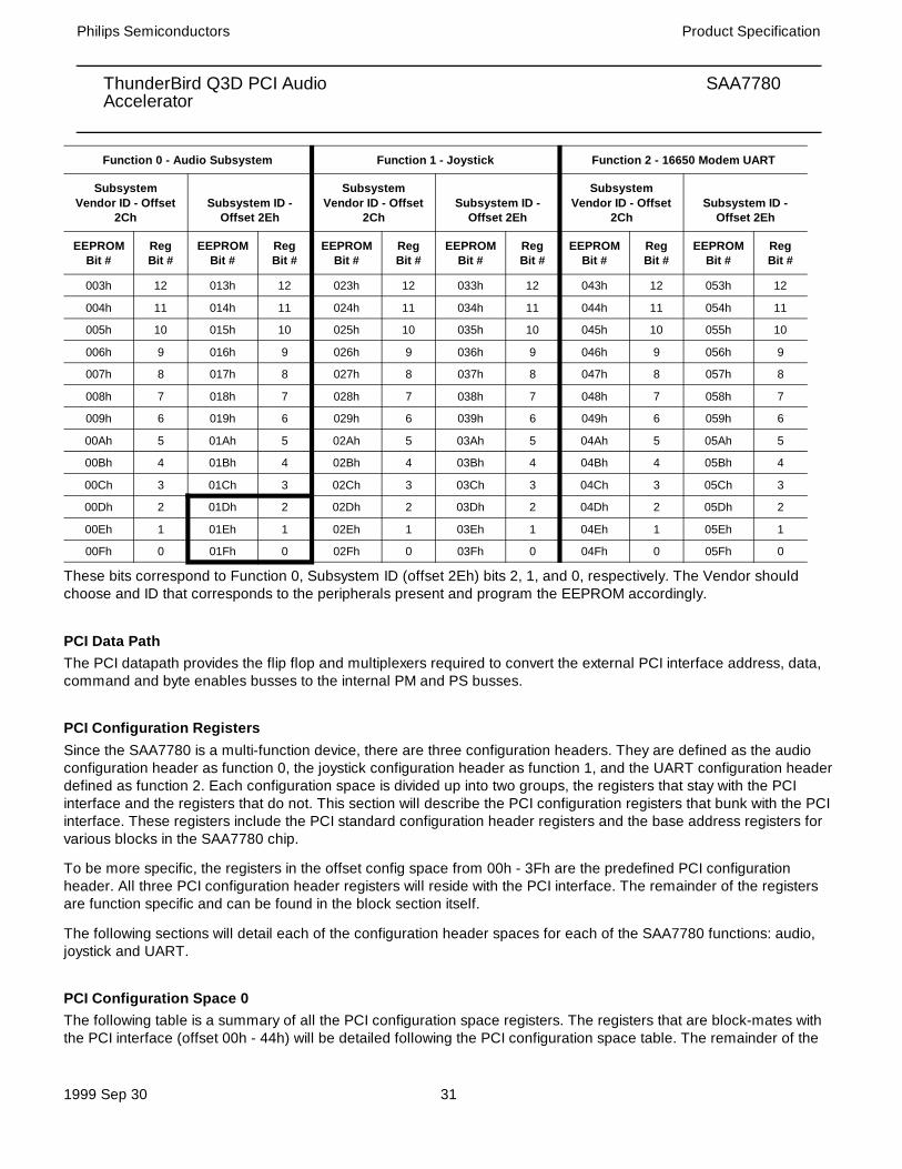
In each of the three SAA7780 functions PCI configuration space there is a Subsystem Vendor ID register at an offset of 2Ch and a Subsystem ID register at an offset of 2Eh. Each register is 16 bits in length and is write-only by the serial EEPROM and read-only from the PCI interface. The data from the EEPROM is loaded into the registers immediately after PCI reset. If no EEPROM is detected, the default values are loaded as shown and reflect the default values for the System ID and Vendor ID for that function.
Subsystem Register Default Values
The EEPROM contains bits 000h through 3FFh. Only bits 000h through 05Fh are utilized to program the Subsystem ID and Subsystem Vendor ID registers. The bit assignments between the EEPROM and the configuration registers are shown below.
EEPROM BIT Assignments to Subsystem Registers
Function Device Type Offset Register Name Default Value
0 Audio Subsystem 2Ch Subsystem Vendor ID 1004h
0 Audio Subsystem 2Eh Subsystem ID 0304h
1 Joystick 2Ch Subsystem Vendor ID 1004h
1 Joystick 2Eh Subsystem ID 0305h
2 16650 UART 2Ch Subsystem Vendor ID 1004h
2 16650 UART 2Eh Subsystem ID 0306h
Function 0 - Audio Subsystem Function 1 - Joystick Function 2 - 16650 Modem UART
Subsystem Vendor ID - Offset
2ChSubsystem ID -
Offset 2Eh
Subsystem Vendor ID - Offset
2ChSubsystem ID -
Offset 2Eh
Subsystem Vendor ID - Offset
2ChSubsystem ID -
Offset 2Eh
EEPROM Bit #
Reg Bit #
EEPROM Bit #
Reg Bit #
EEPROM Bit #
Reg Bit #
EEPROM Bit #
Reg Bit #
EEPROM Bit #
Reg Bit #
EEPROM Bit #
Reg Bit #
000h 15 010h 15 020h 15 030h 15 040h 15 050h 15
001h 14 011h 14 021h 14 031h 14 041h 14 051h 14
002h 13 012h 13 022h 13 032h 13 042h 13 052h 13
ThunderBird EEPROM
CFGDAT
CFGCLK
SDA
SCL
WP
+5V

ThunderBird Q3D PCI Audio SAA7780Accelerator
Philips Semiconductors Product Specification
1999 Sep 30 31
These bits correspond to Function 0, Subsystem ID (offset 2Eh) bits 2, 1, and 0, respectively. The Vendor should choose and ID that corresponds to the peripherals present and program the EEPROM accordingly.
PCI Data Path The PCI datapath provides the flip flop and multiplexers required to convert the external PCI interface address, data, command and byte enables busses to the internal PM and PS busses.
PCI Configuration Registers Since the SAA7780 is a multi-function device, there are three configuration headers. They are defined as the audio configuration header as function 0, the joystick configuration header as function 1, and the UART configuration header defined as function 2. Each configuration space is divided up into two groups, the registers that stay with the PCI interface and the registers that do not. This section will describe the PCI configuration registers that bunk with the PCI interface. These registers include the PCI standard configuration header registers and the base address registers for various blocks in the SAA7780 chip.
To be more specific, the registers in the offset config space from 00h - 3Fh are the predefined PCI configuration header. All three PCI configuration header registers will reside with the PCI interface. The remainder of the registers are function specific and can be found in the block section itself.
The following sections will detail each of the configuration header spaces for each of the SAA7780 functions: audio, joystick and UART.
PCI Configuration Space 0 The following table is a summary of all the PCI configuration space registers. The registers that are block-mates with the PCI interface (offset 00h - 44h) will be detailed following the PCI configuration space table. The remainder of the
003h 12 013h 12 023h 12 033h 12 043h 12 053h 12
004h 11 014h 11 024h 11 034h 11 044h 11 054h 11
005h 10 015h 10 025h 10 035h 10 045h 10 055h 10
006h 9 016h 9 026h 9 036h 9 046h 9 056h 9
007h 8 017h 8 027h 8 037h 8 047h 8 057h 8
008h 7 018h 7 028h 7 038h 7 048h 7 058h 7
009h 6 019h 6 029h 6 039h 6 049h 6 059h 6
00Ah 5 01Ah 5 02Ah 5 03Ah 5 04Ah 5 05Ah 5
00Bh 4 01Bh 4 02Bh 4 03Bh 4 04Bh 4 05Bh 4
00Ch 3 01Ch 3 02Ch 3 03Ch 3 04Ch 3 05Ch 3
00Dh 2 01Dh 2 02Dh 2 03Dh 2 04Dh 2 05Dh 2
00Eh 1 01Eh 1 02Eh 1 03Eh 1 04Eh 1 05Eh 1
00Fh 0 01Fh 0 02Fh 0 03Fh 0 04Fh 0 05Fh 0
Function 0 - Audio Subsystem Function 1 - Joystick Function 2 - 16650 Modem UART
Subsystem Vendor ID - Offset
2ChSubsystem ID -
Offset 2Eh
Subsystem Vendor ID - Offset
2ChSubsystem ID -
Offset 2Eh
Subsystem Vendor ID - Offset
2ChSubsystem ID -
Offset 2Eh
EEPROM Bit #
Reg Bit #
EEPROM Bit #
Reg Bit #
EEPROM Bit #
Reg Bit #
EEPROM Bit #
Reg Bit #
EEPROM Bit #
Reg Bit #
EEPROM Bit #
Reg Bit #
ThunderBird Q3D PCI Audio SAA7780Accelerator
Philips Semiconductors Product Specification
1999 Sep 30 32
registers will be detailed with the blocks they control.
PCI Configuration Space 0 Register Map
Byte 3 Byte 2 Byte 1 Byte 0 OffsetDevice ID Vendor ID 00h
Status Command 04hClass Code Revision ID 08h
BIST Header Type Master Latency Timer Cache Line Size 0ChSONGBASE 10h
SBBASE 14h
MDBASE 18hALBASE 1ChReserved 20-2Bh
SUBSYSTEM ID SUBSYSTEM VENDOR ID 2ChReserved 30-3Bh
Max_Lat Min_Gnt Interrupt Pin Interrupt Line 3Ch
DMABBASE DMAABASE 40hReserved 44-57h
Reserved Reserved Reserved MSCCFG 58h
Reserved Reserved Reserved ACLCFG0 5ChReserved Reserved VRCFG 60hReserved Reserved Reserved TIMRCFG0 64h
Reserved Reserved HDCFG 68hReserved 6Ch
Reserved Reserved DMACFG 70h
Reserved 74-77hReserved Reserved Reserved DPLLCTL0 78hReserved Reserved Reserved DPLLCTL1 7Ch
Reserved Reserved Reserved DPLLCTL2 80hReserved 84-87h
Reserved Reserved Reserved TESTCTL0 88h
Reserved 8C-8FhhTBLBASE0 90hTBLBASE1 94h
TBLBASE2 98hTBLBASE3 9Ch
Reserved Reserved Reserved IRQCTL0 A0h
Reserved Reserved Reserved IRQCTL1 A4hReserved Reserved Reserved IRQCTL2 A8hReserved Reserved Reserved IRQCTL3 ACh
Reserved Reserved Reserved IRQCTL4 B0hReserved Reserved Reserved IRQCTL5 B4hReserved Reserved Reserved IRQCTL6 B8h
ThunderBird Q3D PCI Audio SAA7780Accelerator
Philips Semiconductors Product Specification
1999 Sep 30 33
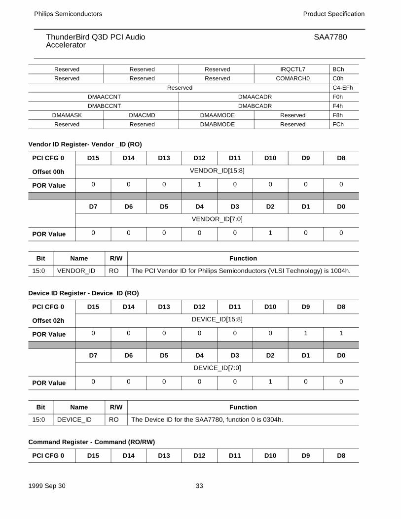
Vendor ID Register- Vendor _ID (RO)
Device ID Register - Device_ID (RO)
Command Register - Command (RO/RW)
Reserved Reserved Reserved IRQCTL7 BChReserved Reserved Reserved COMARCH0 C0h
Reserved C4-EFhDMAACCNT DMAACADR F0hDMABCCNT DMABCADR F4h
DMAMASK DMACMD DMAAMODE Reserved F8hReserved Reserved DMABMODE Reserved FCh
PCI CFG 0 D15 D14 D13 D12 D11 D10 D9 D8
Offset 00h VENDOR_ID[15:8]
POR Value 0 0 0 1 0 0 0 0
D7 D6 D5 D4 D3 D2 D1 D0
VENDOR_ID[7:0]
POR Value 0 0 0 0 0 1 0 0
Bit Name R/W Function
15:0 VENDOR_ID RO The PCI Vendor ID for Philips Semiconductors (VLSI Technology) is 1004h.
PCI CFG 0 D15 D14 D13 D12 D11 D10 D9 D8
Offset 02h DEVICE_ID[15:8]
POR Value 0 0 0 0 0 0 1 1
D7 D6 D5 D4 D3 D2 D1 D0
DEVICE_ID[7:0]
POR Value 0 0 0 0 0 1 0 0
Bit Name R/W Function
15:0 DEVICE_ID RO The Device ID for the SAA7780, function 0 is 0304h.
PCI CFG 0 D15 D14 D13 D12 D11 D10 D9 D8
ThunderBird Q3D PCI Audio SAA7780Accelerator
Philips Semiconductors Product Specification
1999 Sep 30 34
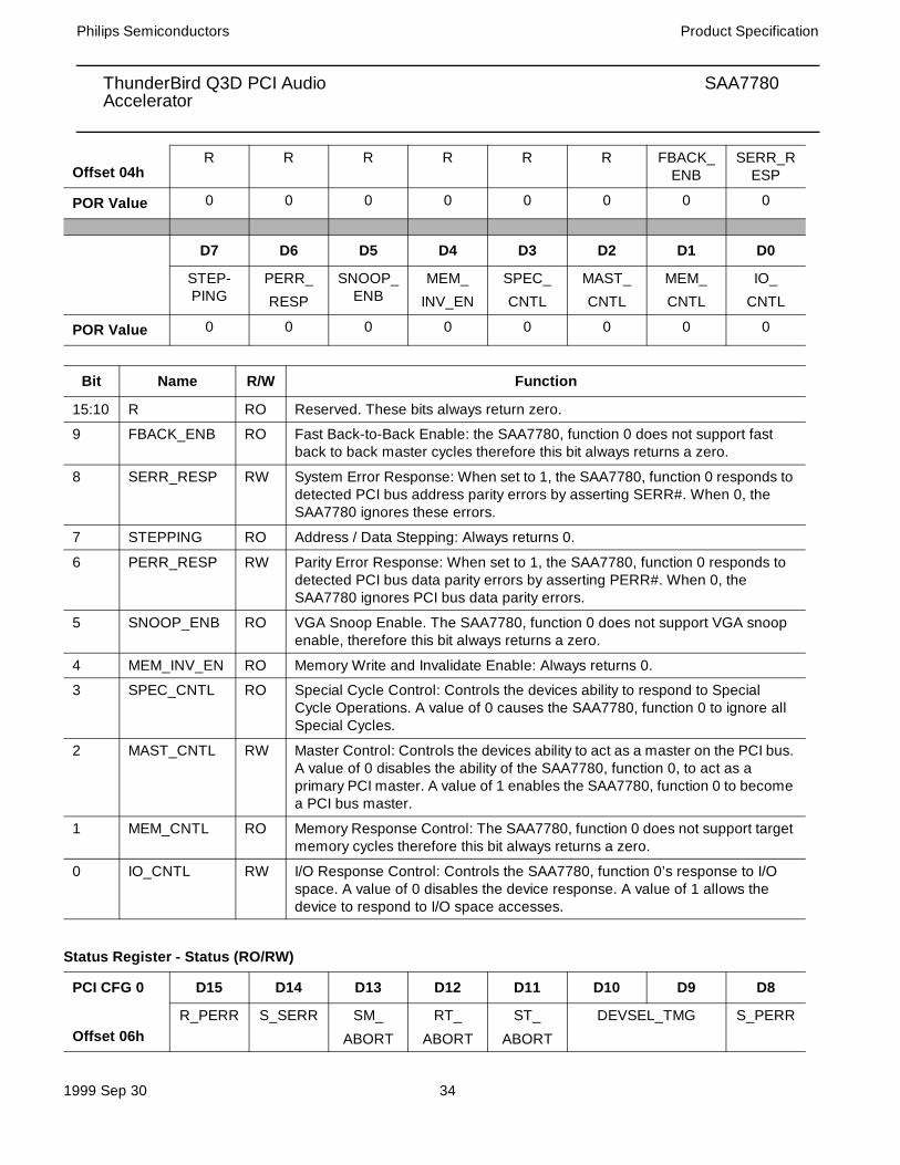
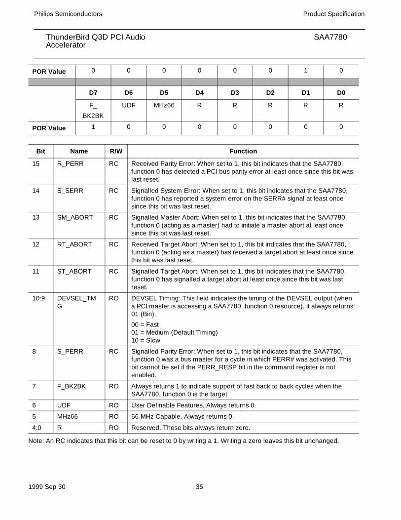
Status Register - Status (RO/RW)
Offset 04hR R R R R R FBACK_
ENBSERR_R
ESP
POR Value 0 0 0 0 0 0 0 0
D7 D6 D5 D4 D3 D2 D1 D0
STEP-PING
PERR_
RESP
SNOOP_ENB
MEM_
INV_EN
SPEC_
CNTL
MAST_
CNTL
MEM_
CNTL
IO_
CNTL
POR Value 0 0 0 0 0 0 0 0
Bit Name R/W Function
15:10 R RO Reserved. These bits always return zero.
9 FBACK_ENB RO Fast Back-to-Back Enable: the SAA7780, function 0 does not support fast back to back master cycles therefore this bit always returns a zero.
8 SERR_RESP RW System Error Response: When set to 1, the SAA7780, function 0 responds to detected PCI bus address parity errors by asserting SERR#. When 0, the SAA7780 ignores these errors.
7 STEPPING RO Address / Data Stepping: Always returns 0.
6 PERR_RESP RW Parity Error Response: When set to 1, the SAA7780, function 0 responds to detected PCI bus data parity errors by asserting PERR#. When 0, the SAA7780 ignores PCI bus data parity errors.
5 SNOOP_ENB RO VGA Snoop Enable. The SAA7780, function 0 does not support VGA snoop enable, therefore this bit always returns a zero.
4 MEM_INV_EN RO Memory Write and Invalidate Enable: Always returns 0.
3 SPEC_CNTL RO Special Cycle Control: Controls the devices ability to respond to Special Cycle Operations. A value of 0 causes the SAA7780, function 0 to ignore all Special Cycles.
2 MAST_CNTL RW Master Control: Controls the devices ability to act as a master on the PCI bus. A value of 0 disables the ability of the SAA7780, function 0, to act as a primary PCI master. A value of 1 enables the SAA7780, function 0 to become a PCI bus master.
1 MEM_CNTL RO Memory Response Control: The SAA7780, function 0 does not support target memory cycles therefore this bit always returns a zero.
0 IO_CNTL RW I/O Response Control: Controls the SAA7780, function 0’s response to I/O space. A value of 0 disables the device response. A value of 1 allows the device to respond to I/O space accesses.
PCI CFG 0 D15 D14 D13 D12 D11 D10 D9 D8
Offset 06hR_PERR S_SERR SM_
ABORT
RT_
ABORT
ST_
ABORT
DEVSEL_TMG S_PERR
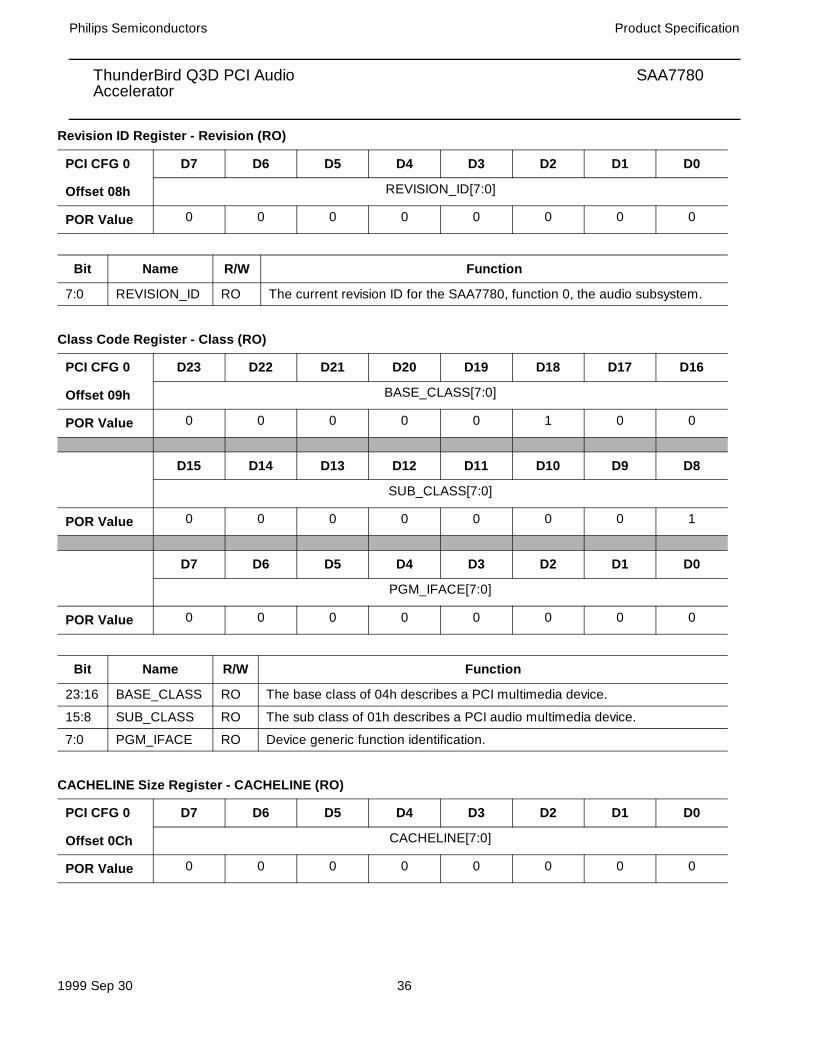
ThunderBird Q3D PCI Audio SAA7780Accelerator
Philips Semiconductors Product Specification
1999 Sep 30 35
Note: An RC indicates that this bit can be reset to 0 by writing a 1. Writing a zero leaves this bit unchanged.
POR Value 0 0 0 0 0 0 1 0
D7 D6 D5 D4 D3 D2 D1 D0
F_
BK2BK
UDF MHz66 R R R R R
POR Value 1 0 0 0 0 0 0 0
Bit Name R/W Function
15 R_PERR RC Received Parity Error: When set to 1, this bit indicates that the SAA7780, function 0 has detected a PCI bus parity error at least once since this bit was last reset.
14 S_SERR RC Signalled System Error: When set to 1, this bit indicates that the SAA7780, function 0 has reported a system error on the SERR# signal at least once since this bit was last reset.
13 SM_ABORT RC Signalled Master Abort: When set to 1, this bit indicates that the SAA7780, function 0 (acting as a master) had to initiate a master abort at least once since this bit was last reset.
12 RT_ABORT RC Received Target Abort: When set to 1, this bit indicates that the SAA7780, function 0 (acting as a master) has received a target abort at least once since this bit was last reset.
11 ST_ABORT RC Signalled Target Abort: When set to 1, this bit indicates that the SAA7780, function 0 has signalled a target abort at least once since this bit was last reset.
10:9 DEVSEL_TMG
RO DEVSEL Timing: This field indicates the timing of the DEVSEL output (when a PCI master is accessing a SAA7780, function 0 resource). It always returns 01 (Bin).
00 = Fast01 = Medium (Default Timing)10 = Slow
8 S_PERR RC Signalled Parity Error: When set to 1, this bit indicates that the SAA7780, function 0 was a bus master for a cycle in which PERR# was activated. This bit cannot be set if the PERR_RESP bit in the command register is not enabled.
7 F_BK2BK RO Always returns 1 to indicate support of fast back to back cycles when the SAA7780, function 0 is the target.
6 UDF RO User Definable Features. Always returns 0.
5 MHz66 RO 66 MHz Capable. Always returns 0.
4:0 R RO Reserved. These bits always return zero.
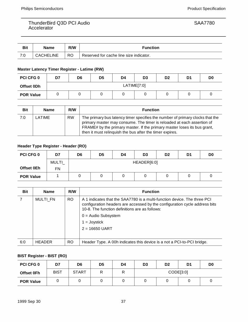
ThunderBird Q3D PCI Audio SAA7780Accelerator
Philips Semiconductors Product Specification
1999 Sep 30 36
Revision ID Register - Revision (RO)
Class Code Register - Class (RO)
CACHELINE Size Register - CACHELINE (RO)
PCI CFG 0 D7 D6 D5 D4 D3 D2 D1 D0
Offset 08h REVISION_ID[7:0]
POR Value 0 0 0 0 0 0 0 0
Bit Name R/W Function
7:0 REVISION_ID RO The current revision ID for the SAA7780, function 0, the audio subsystem.
PCI CFG 0 D23 D22 D21 D20 D19 D18 D17 D16
Offset 09h BASE_CLASS[7:0]
POR Value 0 0 0 0 0 1 0 0
D15 D14 D13 D12 D11 D10 D9 D8
SUB_CLASS[7:0]
POR Value 0 0 0 0 0 0 0 1
D7 D6 D5 D4 D3 D2 D1 D0
PGM_IFACE[7:0]
POR Value 0 0 0 0 0 0 0 0
Bit Name R/W Function
23:16 BASE_CLASS RO The base class of 04h describes a PCI multimedia device.
15:8 SUB_CLASS RO The sub class of 01h describes a PCI audio multimedia device.
7:0 PGM_IFACE RO Device generic function identification.
PCI CFG 0 D7 D6 D5 D4 D3 D2 D1 D0
Offset 0Ch CACHELINE[7:0]
POR Value 0 0 0 0 0 0 0 0
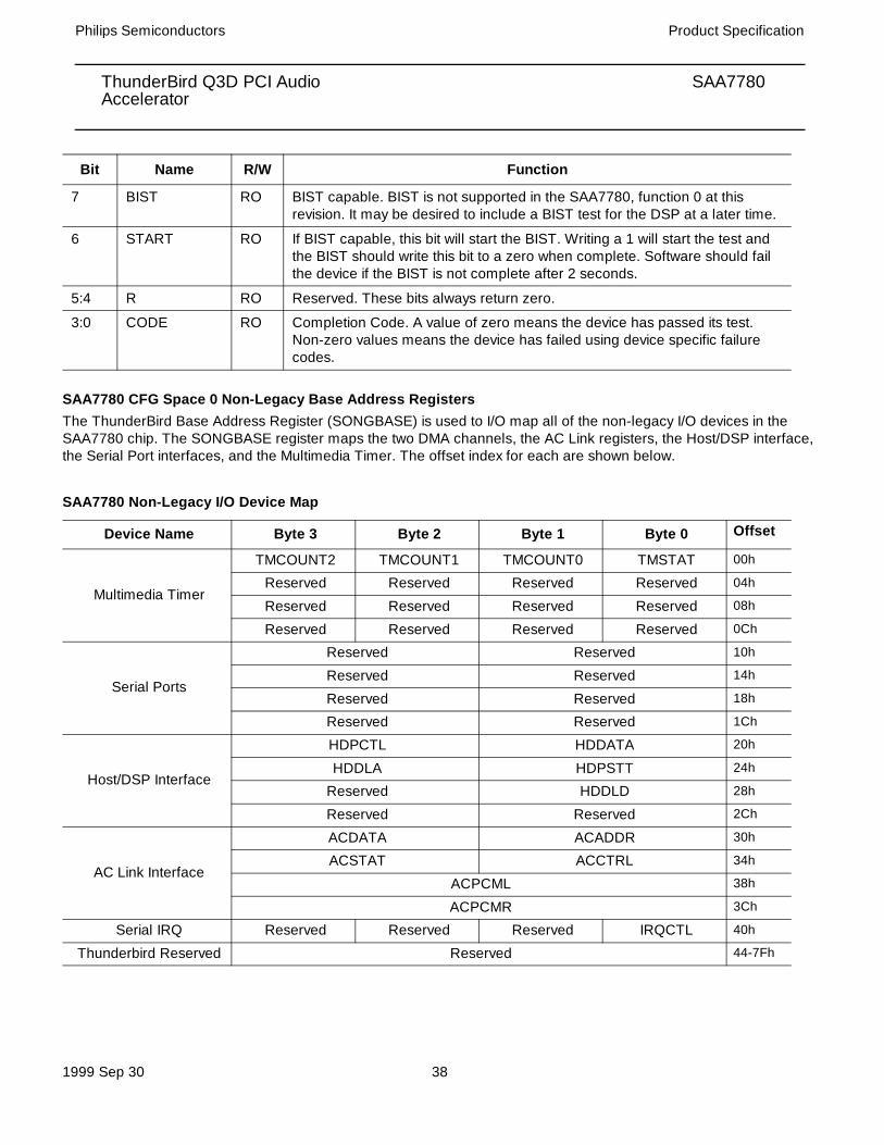
ThunderBird Q3D PCI Audio SAA7780Accelerator
Philips Semiconductors Product Specification
1999 Sep 30 37
Master Latency Timer Register - Latime (RW)
Header Type Register - Header (RO)
BIST Register - BIST (RO)
Bit Name R/W Function
7:0 CACHELINE RO Reserved for cache line size indicator.
PCI CFG 0 D7 D6 D5 D4 D3 D2 D1 D0
Offset 0Dh LATIME[7:0]
POR Value 0 0 0 0 0 0 0 0
Bit Name R/W Function
7:0 LATIME RW The primary bus latency timer specifies the number of primary clocks that the primary master may consume. The timer is reloaded at each assertion of FRAME# by the primary master. If the primary master loses its bus grant, then it must relinquish the bus after the timer expires.
PCI CFG 0 D7 D6 D5 D4 D3 D2 D1 D0
Offset 0EhMULTI_
FN
HEADER[6:0]
POR Value 1 0 0 0 0 0 0 0
Bit Name R/W Function
7 MULTI_FN RO A 1 indicates that the SAA7780 is a multi-function device. The three PCI configuration headers are accessed by the configuration cycle address bits 10-8. The function definitions are as follows:
0 = Audio Subsystem
1 = Joystick
2 = 16650 UART
6:0 HEADER RO Header Type. A 00h indicates this device is a not a PCI-to-PCI bridge.
PCI CFG 0 D7 D6 D5 D4 D3 D2 D1 D0
Offset 0Fh BIST START R R CODE[3:0]
POR Value 0 0 0 0 0 0 0 0
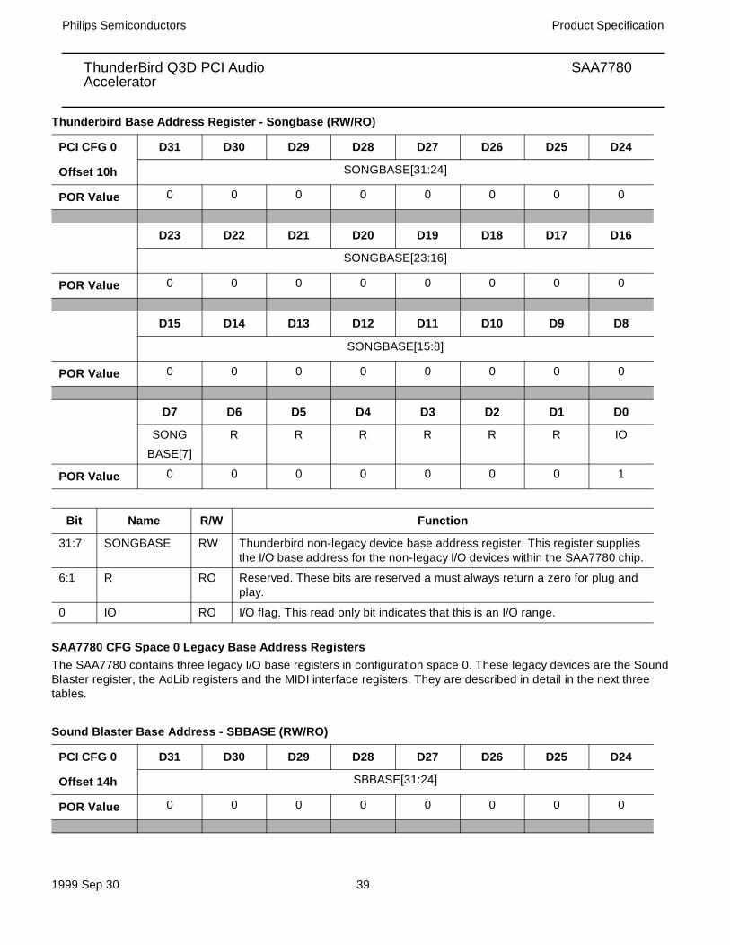
ThunderBird Q3D PCI Audio SAA7780Accelerator
Philips Semiconductors Product Specification
1999 Sep 30 38
SAA7780 CFG Space 0 Non-Legacy Base Address RegistersThe ThunderBird Base Address Register (SONGBASE) is used to I/O map all of the non-legacy I/O devices in the SAA7780 chip. The SONGBASE register maps the two DMA channels, the AC Link registers, the Host/DSP interface, the Serial Port interfaces, and the Multimedia Timer. The offset index for each are shown below.
SAA7780 Non-Legacy I/O Device Map
Bit Name R/W Function
7 BIST RO BIST capable. BIST is not supported in the SAA7780, function 0 at this revision. It may be desired to include a BIST test for the DSP at a later time.
6 START RO If BIST capable, this bit will start the BIST. Writing a 1 will start the test and the BIST should write this bit to a zero when complete. Software should fail the device if the BIST is not complete after 2 seconds.
5:4 R RO Reserved. These bits always return zero.
3:0 CODE RO Completion Code. A value of zero means the device has passed its test. Non-zero values means the device has failed using device specific failure codes.
Device Name Byte 3 Byte 2 Byte 1 Byte 0 Offset
Multimedia Timer
TMCOUNT2 TMCOUNT1 TMCOUNT0 TMSTAT 00h
Reserved Reserved Reserved Reserved 04h
Reserved Reserved Reserved Reserved 08h
Reserved Reserved Reserved Reserved 0Ch
Serial Ports
Reserved Reserved 10h
Reserved Reserved 14h
Reserved Reserved 18h
Reserved Reserved 1Ch
Host/DSP Interface
HDPCTL HDDATA 20h
HDDLA HDPSTT 24h
Reserved HDDLD 28h
Reserved Reserved 2Ch
AC Link Interface
ACDATA ACADDR 30h
ACSTAT ACCTRL 34h
ACPCML 38h
ACPCMR 3Ch
Serial IRQ Reserved Reserved Reserved IRQCTL 40h
Thunderbird Reserved Reserved 44-7Fh
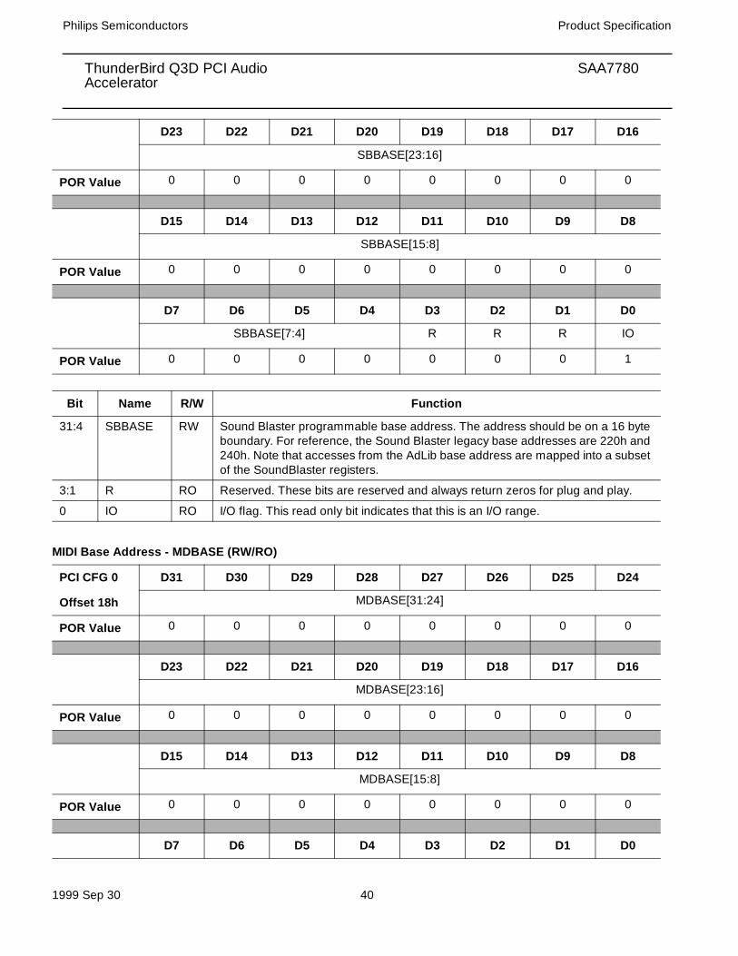
ThunderBird Q3D PCI Audio SAA7780Accelerator
Philips Semiconductors Product Specification
1999 Sep 30 39
Thunderbird Base Address Register - Songbase (RW/RO)
SAA7780 CFG Space 0 Legacy Base Address Registers The SAA7780 contains three legacy I/O base registers in configuration space 0. These legacy devices are the Sound Blaster register, the AdLib registers and the MIDI interface registers. They are described in detail in the next three tables.
Sound Blaster Base Address - SBBASE (RW/RO)
PCI CFG 0 D31 D30 D29 D28 D27 D26 D25 D24
Offset 10h SONGBASE[31:24]
POR Value 0 0 0 0 0 0 0 0
D23 D22 D21 D20 D19 D18 D17 D16
SONGBASE[23:16]
POR Value 0 0 0 0 0 0 0 0
D15 D14 D13 D12 D11 D10 D9 D8
SONGBASE[15:8]
POR Value 0 0 0 0 0 0 0 0
D7 D6 D5 D4 D3 D2 D1 D0
SONG
BASE[7]
R R R R R R IO
POR Value 0 0 0 0 0 0 0 1
Bit Name R/W Function
31:7 SONGBASE RW Thunderbird non-legacy device base address register. This register supplies the I/O base address for the non-legacy I/O devices within the SAA7780 chip.
6:1 R RO Reserved. These bits are reserved a must always return a zero for plug and play.
0 IO RO I/O flag. This read only bit indicates that this is an I/O range.
PCI CFG 0 D31 D30 D29 D28 D27 D26 D25 D24
Offset 14h SBBASE[31:24]
POR Value 0 0 0 0 0 0 0 0
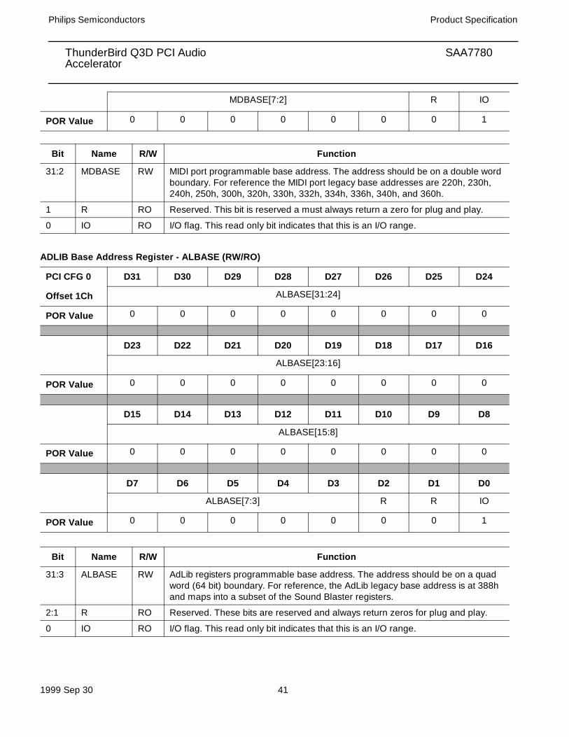
ThunderBird Q3D PCI Audio SAA7780Accelerator
Philips Semiconductors Product Specification
1999 Sep 30 40
MIDI Base Address - MDBASE (RW/RO)
D23 D22 D21 D20 D19 D18 D17 D16
SBBASE[23:16]
POR Value 0 0 0 0 0 0 0 0
D15 D14 D13 D12 D11 D10 D9 D8
SBBASE[15:8]
POR Value 0 0 0 0 0 0 0 0
D7 D6 D5 D4 D3 D2 D1 D0
SBBASE[7:4] R R R IO
POR Value 0 0 0 0 0 0 0 1
Bit Name R/W Function
31:4 SBBASE RW Sound Blaster programmable base address. The address should be on a 16 byte boundary. For reference, the Sound Blaster legacy base addresses are 220h and 240h. Note that accesses from the AdLib base address are mapped into a subset of the SoundBlaster registers.
3:1 R RO Reserved. These bits are reserved and always return zeros for plug and play.
0 IO RO I/O flag. This read only bit indicates that this is an I/O range.
PCI CFG 0 D31 D30 D29 D28 D27 D26 D25 D24
Offset 18h MDBASE[31:24]
POR Value 0 0 0 0 0 0 0 0
D23 D22 D21 D20 D19 D18 D17 D16
MDBASE[23:16]
POR Value 0 0 0 0 0 0 0 0
D15 D14 D13 D12 D11 D10 D9 D8
MDBASE[15:8]
POR Value 0 0 0 0 0 0 0 0
D7 D6 D5 D4 D3 D2 D1 D0
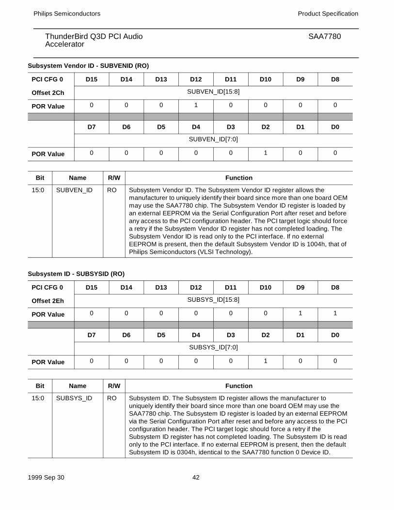
ThunderBird Q3D PCI Audio SAA7780Accelerator
Philips Semiconductors Product Specification
1999 Sep 30 41
ADLIB Base Address Register - ALBASE (RW/RO)
MDBASE[7:2] R IO
POR Value 0 0 0 0 0 0 0 1
Bit Name R/W Function
31:2 MDBASE RW MIDI port programmable base address. The address should be on a double word boundary. For reference the MIDI port legacy base addresses are 220h, 230h, 240h, 250h, 300h, 320h, 330h, 332h, 334h, 336h, 340h, and 360h.
1 R RO Reserved. This bit is reserved a must always return a zero for plug and play.
0 IO RO I/O flag. This read only bit indicates that this is an I/O range.
PCI CFG 0 D31 D30 D29 D28 D27 D26 D25 D24
Offset 1Ch ALBASE[31:24]
POR Value 0 0 0 0 0 0 0 0
D23 D22 D21 D20 D19 D18 D17 D16
ALBASE[23:16]
POR Value 0 0 0 0 0 0 0 0
D15 D14 D13 D12 D11 D10 D9 D8
ALBASE[15:8]
POR Value 0 0 0 0 0 0 0 0
D7 D6 D5 D4 D3 D2 D1 D0
ALBASE[7:3] R R IO
POR Value 0 0 0 0 0 0 0 1
Bit Name R/W Function
31:3 ALBASE RW AdLib registers programmable base address. The address should be on a quad word (64 bit) boundary. For reference, the AdLib legacy base address is at 388h and maps into a subset of the Sound Blaster registers.
2:1 R RO Reserved. These bits are reserved and always return zeros for plug and play.
0 IO RO I/O flag. This read only bit indicates that this is an I/O range.
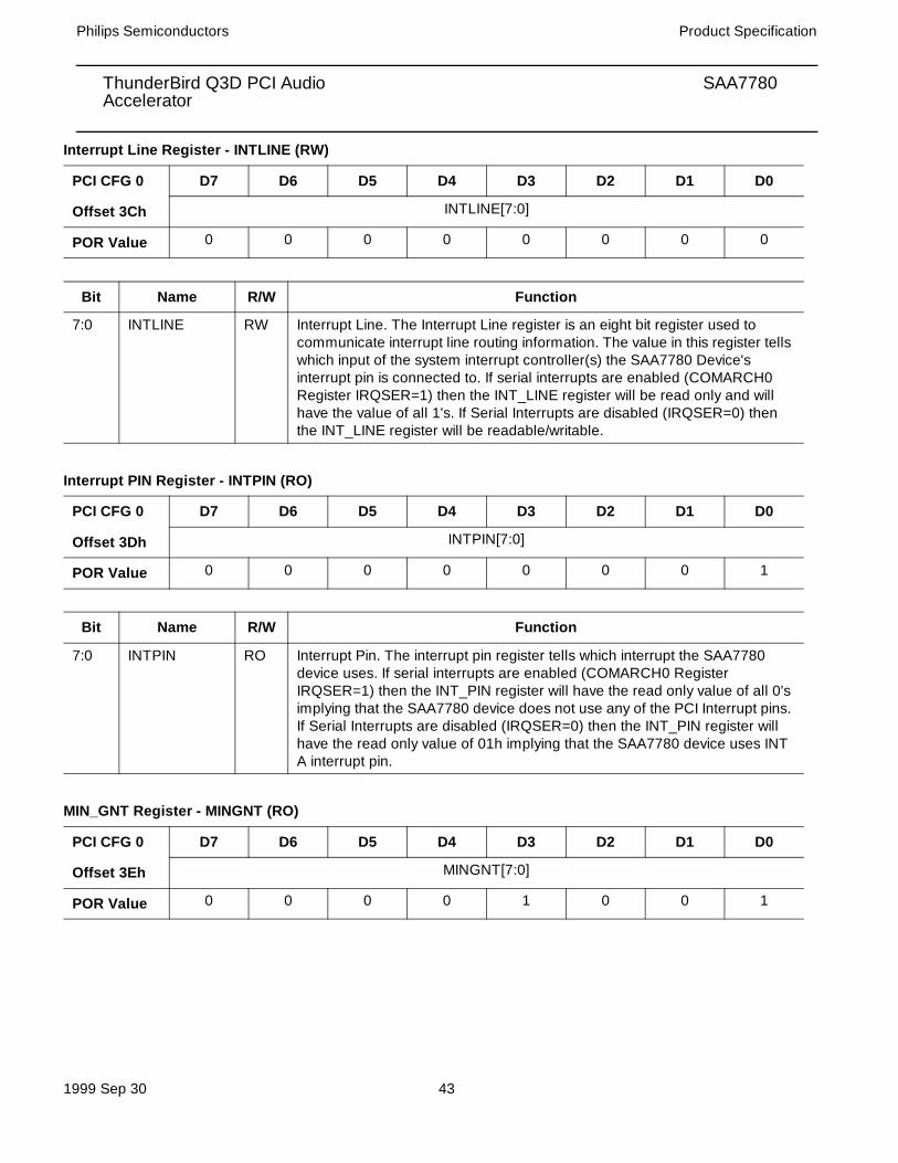
ThunderBird Q3D PCI Audio SAA7780Accelerator
Philips Semiconductors Product Specification
1999 Sep 30 42
Subsystem Vendor ID - SUBVENID (RO)
Subsystem ID - SUBSYSID (RO)
PCI CFG 0 D15 D14 D13 D12 D11 D10 D9 D8
Offset 2Ch SUBVEN_ID[15:8]
POR Value 0 0 0 1 0 0 0 0
D7 D6 D5 D4 D3 D2 D1 D0
SUBVEN_ID[7:0]
POR Value 0 0 0 0 0 1 0 0
Bit Name R/W Function
15:0 SUBVEN_ID RO Subsystem Vendor ID. The Subsystem Vendor ID register allows the manufacturer to uniquely identify their board since more than one board OEM may use the SAA7780 chip. The Subsystem Vendor ID register is loaded by an external EEPROM via the Serial Configuration Port after reset and before any access to the PCI configuration header. The PCI target logic should force a retry if the Subsystem Vendor ID register has not completed loading. The Subsystem Vendor ID is read only to the PCI interface. If no external EEPROM is present, then the default Subsystem Vendor ID is 1004h, that of Philips Semiconductors (VLSI Technology).
PCI CFG 0 D15 D14 D13 D12 D11 D10 D9 D8
Offset 2Eh SUBSYS_ID[15:8]
POR Value 0 0 0 0 0 0 1 1
D7 D6 D5 D4 D3 D2 D1 D0
SUBSYS_ID[7:0]
POR Value 0 0 0 0 0 1 0 0
Bit Name R/W Function
15:0 SUBSYS_ID RO Subsystem ID. The Subsystem ID register allows the manufacturer to uniquely identify their board since more than one board OEM may use the SAA7780 chip. The Subsystem ID register is loaded by an external EEPROM via the Serial Configuration Port after reset and before any access to the PCI configuration header. The PCI target logic should force a retry if the Subsystem ID register has not completed loading. The Subsystem ID is read only to the PCI interface. If no external EEPROM is present, then the default Subsystem ID is 0304h, identical to the SAA7780 function 0 Device ID.
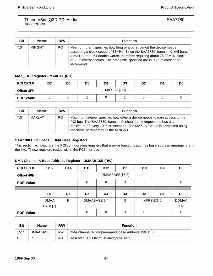
ThunderBird Q3D PCI Audio SAA7780Accelerator
Philips Semiconductors Product Specification
1999 Sep 30 43
Interrupt Line Register - INTLINE (RW)
Interrupt PIN Register - INTPIN (RO)
MIN_GNT Register - MINGNT (RO)
PCI CFG 0 D7 D6 D5 D4 D3 D2 D1 D0
Offset 3Ch INTLINE[7:0]
POR Value 0 0 0 0 0 0 0 0
Bit Name R/W Function
7:0 INTLINE RW Interrupt Line. The Interrupt Line register is an eight bit register used to communicate interrupt line routing information. The value in this register tells which input of the system interrupt controller(s) the SAA7780 Device's interrupt pin is connected to. If serial interrupts are enabled (COMARCH0 Register IRQSER=1) then the INT_LINE register will be read only and will have the value of all 1's. If Serial Interrupts are disabled (IRQSER=0) then the INT_LINE register will be readable/writable.
PCI CFG 0 D7 D6 D5 D4 D3 D2 D1 D0
Offset 3Dh INTPIN[7:0]
POR Value 0 0 0 0 0 0 0 1
Bit Name R/W Function
7:0 INTPIN RO Interrupt Pin. The interrupt pin register tells which interrupt the SAA7780 device uses. If serial interrupts are enabled (COMARCH0 Register IRQSER=1) then the INT_PIN register will have the read only value of all 0's implying that the SAA7780 device does not use any of the PCI Interrupt pins. If Serial Interrupts are disabled (IRQSER=0) then the INT_PIN register will have the read only value of 01h implying that the SAA7780 device uses INT A interrupt pin.
PCI CFG 0 D7 D6 D5 D4 D3 D2 D1 D0
Offset 3Eh MINGNT[7:0]
POR Value 0 0 0 0 1 0 0 1
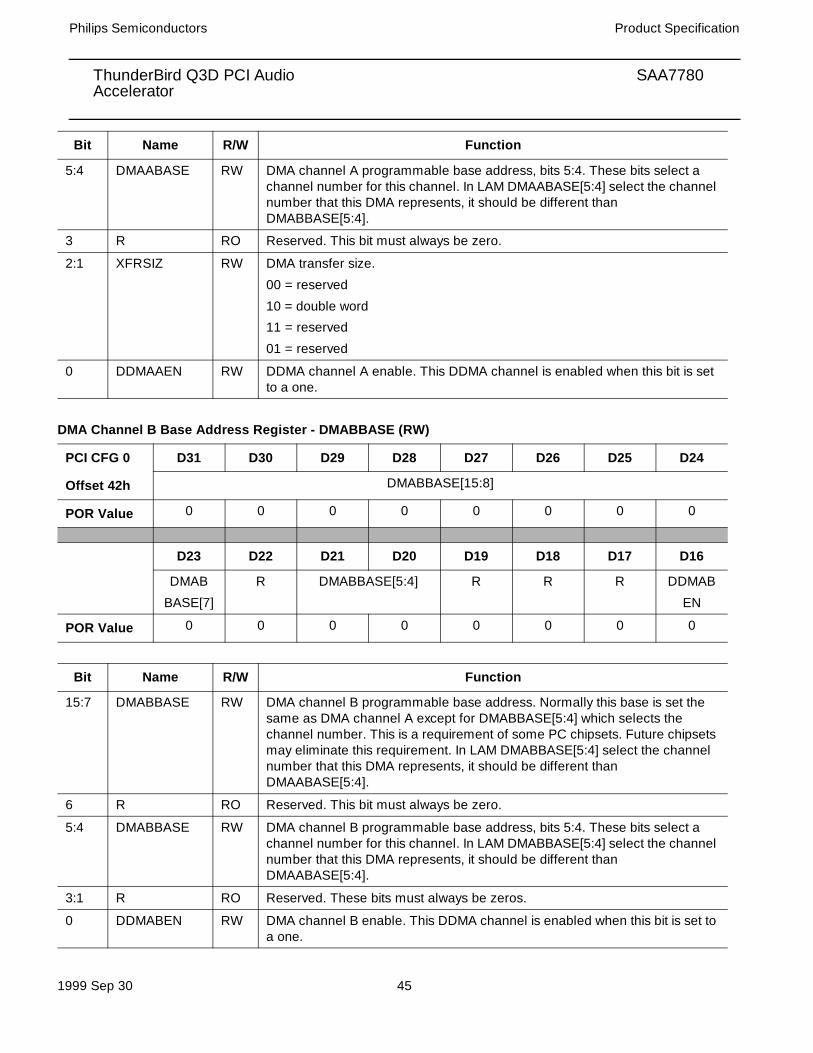
ThunderBird Q3D PCI Audio SAA7780Accelerator
Philips Semiconductors Product Specification
1999 Sep 30 44
MAX_LAT Register - MAXLAT (RO)
SAA7780 CFG Space 0 DMA Base Registers This section will describe the PCI configuration registers that provide functions such as base address remapping and the like. These registers reside within the PCI interface.
DMA Channel A Base Address Register - DMAABASE (RW)
Bit Name R/W Function
7:0 MINGNT RO Minimum grant specifies how long of a burst period the device needs assuming a clock speed of 33MHz. Since the SAA7780, function 0, will burst a maximum of 64 double words, therefore requiring about 75 33MHz clocks or 2.25 microseconds. The time units specified are in 0.25 microsecond increments.
PCI CFG 0 D7 D6 D5 D4 D3 D2 D1 D0
Offset 3Fh MAXLAT[7:0]
POR Value 0 0 1 0 1 0 0 0
Bit Name R/W Function
7:0 MAXLAT RO Maximum latency specifies how often a device needs to gain access to the PCI bus. The SAA7780, function 0, should only request the bus a a maximum of every 10 microseconds. The MAXLAT value is computed using the same parameters as the MINGNT.
PCI CFG 0 D15 D14 D13 D12 D11 D10 D9 D8
Offset 40h DMAABASE[15:8]
POR Value 0 0 0 0 0 0 0 0
D7 D6 D5 D4 D3 D2 D1 D0
DMAA
BASE[7]
R DMAABASE[5:4] R XFRSIZ[1:0] DDMAA
EN
POR Value 0 0 0 0 0 1 0 0
Bit Name R/W Function
15:7 DMAABASE RW DMA channel A programmable base address, bits 15:7.
6 R RO Reserved. This bit must always be zero.
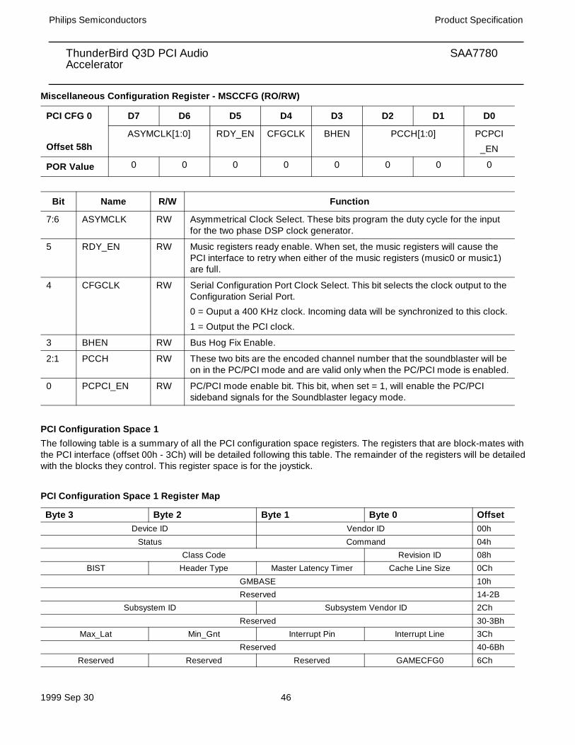
ThunderBird Q3D PCI Audio SAA7780Accelerator
Philips Semiconductors Product Specification
1999 Sep 30 45
DMA Channel B Base Address Register - DMABBASE (RW)
5:4 DMAABASE RW DMA channel A programmable base address, bits 5:4. These bits select a channel number for this channel. In LAM DMAABASE[5:4] select the channel number that this DMA represents, it should be different than DMABBASE[5:4].
3 R RO Reserved. This bit must always be zero.
2:1 XFRSIZ RW DMA transfer size.
00 = reserved
10 = double word
11 = reserved
01 = reserved
0 DDMAAEN RW DDMA channel A enable. This DDMA channel is enabled when this bit is set to a one.
PCI CFG 0 D31 D30 D29 D28 D27 D26 D25 D24
Offset 42h DMABBASE[15:8]
POR Value 0 0 0 0 0 0 0 0
D23 D22 D21 D20 D19 D18 D17 D16
DMAB
BASE[7]
R DMABBASE[5:4] R R R DDMAB
EN
POR Value 0 0 0 0 0 0 0 0
Bit Name R/W Function
15:7 DMABBASE RW DMA channel B programmable base address. Normally this base is set the same as DMA channel A except for DMABBASE[5:4] which selects the channel number. This is a requirement of some PC chipsets. Future chipsets may eliminate this requirement. In LAM DMABBASE[5:4] select the channel number that this DMA represents, it should be different than DMAABASE[5:4].
6 R RO Reserved. This bit must always be zero.
5:4 DMABBASE RW DMA channel B programmable base address, bits 5:4. These bits select a channel number for this channel. In LAM DMABBASE[5:4] select the channel number that this DMA represents, it should be different than DMAABASE[5:4].
3:1 R RO Reserved. These bits must always be zeros.
0 DDMABEN RW DMA channel B enable. This DDMA channel is enabled when this bit is set to a one.
Bit Name R/W Function
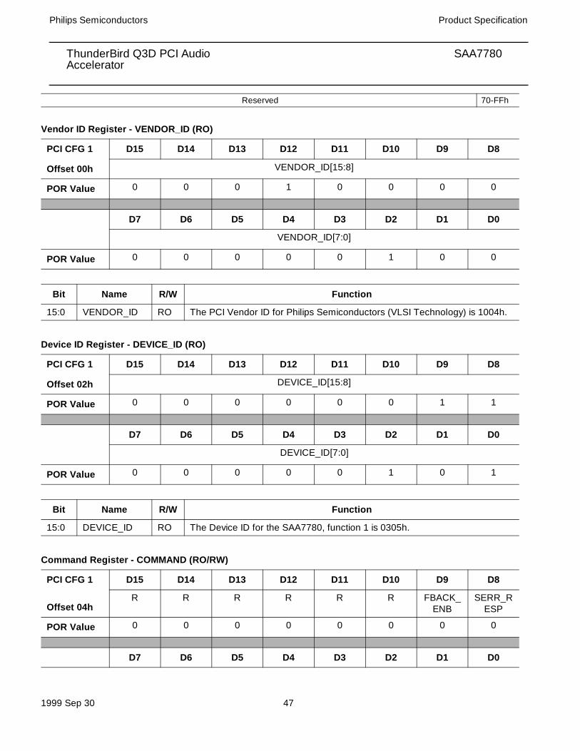
ThunderBird Q3D PCI Audio SAA7780Accelerator
Philips Semiconductors Product Specification
1999 Sep 30 46
Miscellaneous Configuration Register - MSCCFG (RO/RW)
PCI Configuration Space 1The following table is a summary of all the PCI configuration space registers. The registers that are block-mates with the PCI interface (offset 00h - 3Ch) will be detailed following this table. The remainder of the registers will be detailed with the blocks they control. This register space is for the joystick.
PCI Configuration Space 1 Register Map
PCI CFG 0 D7 D6 D5 D4 D3 D2 D1 D0
Offset 58hASYMCLK[1:0] RDY_EN CFGCLK BHEN PCCH[1:0] PCPCI
_EN
POR Value 0 0 0 0 0 0 0 0
Bit Name R/W Function
7:6 ASYMCLK RW Asymmetrical Clock Select. These bits program the duty cycle for the input for the two phase DSP clock generator.
5 RDY_EN RW Music registers ready enable. When set, the music registers will cause the PCI interface to retry when either of the music registers (music0 or music1) are full.
4 CFGCLK RW Serial Configuration Port Clock Select. This bit selects the clock output to the Configuration Serial Port.
0 = Ouput a 400 KHz clock. Incoming data will be synchronized to this clock.
1 = Output the PCI clock.
3 BHEN RW Bus Hog Fix Enable.
2:1 PCCH RW These two bits are the encoded channel number that the soundblaster will be on in the PC/PCI mode and are valid only when the PC/PCI mode is enabled.
0 PCPCI_EN RW PC/PCI mode enable bit. This bit, when set = 1, will enable the PC/PCI sideband signals for the Soundblaster legacy mode.
Byte 3 Byte 2 Byte 1 Byte 0 OffsetDevice ID Vendor ID 00h
Status Command 04hClass Code Revision ID 08h
BIST Header Type Master Latency Timer Cache Line Size 0Ch
GMBASE 10hReserved 14-2B
Subsystem ID Subsystem Vendor ID 2Ch
Reserved 30-3BhMax_Lat Min_Gnt Interrupt Pin Interrupt Line 3Ch
Reserved 40-6Bh
Reserved Reserved Reserved GAMECFG0 6Ch
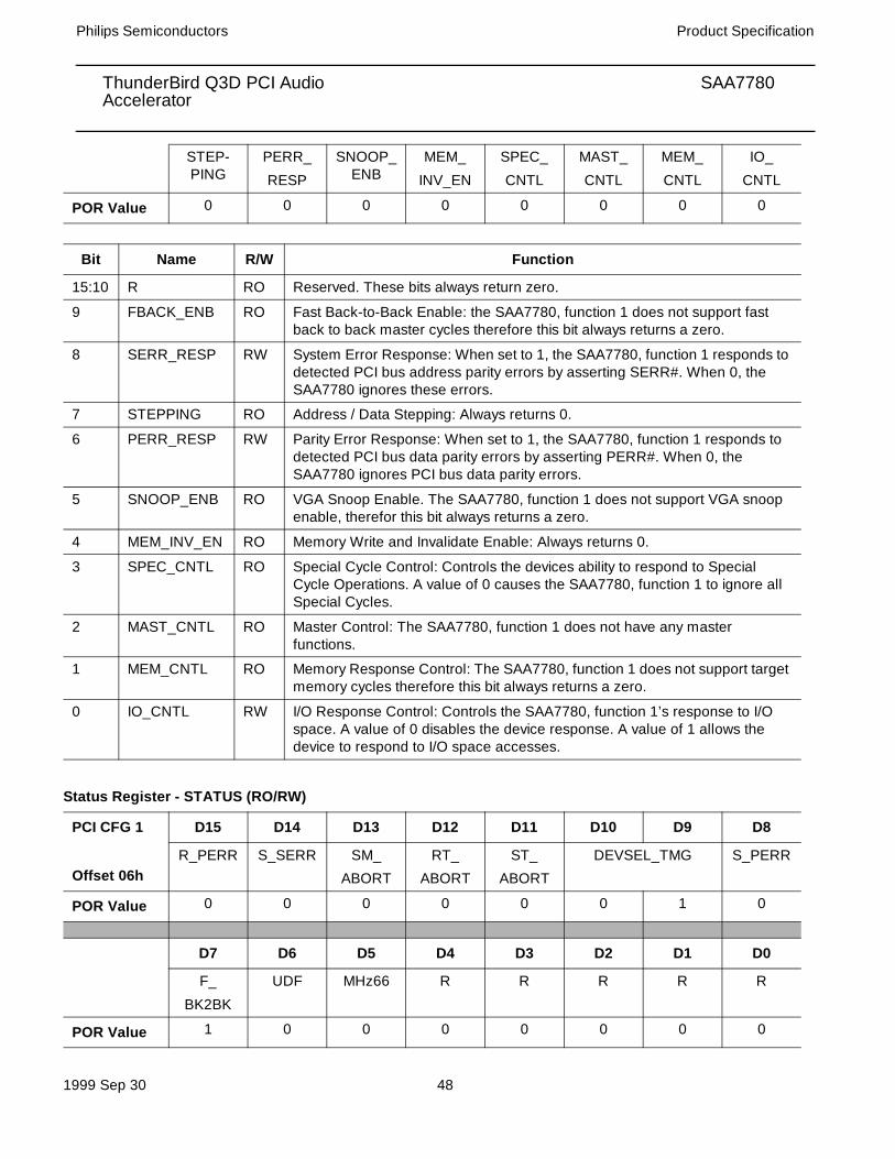
ThunderBird Q3D PCI Audio SAA7780Accelerator
Philips Semiconductors Product Specification
1999 Sep 30 47
Vendor ID Register - VENDOR_ID (RO)
Device ID Register - DEVICE_ID (RO)
Command Register - COMMAND (RO/RW)
Reserved 70-FFh
PCI CFG 1 D15 D14 D13 D12 D11 D10 D9 D8
Offset 00h VENDOR_ID[15:8]
POR Value 0 0 0 1 0 0 0 0
D7 D6 D5 D4 D3 D2 D1 D0
VENDOR_ID[7:0]
POR Value 0 0 0 0 0 1 0 0
Bit Name R/W Function
15:0 VENDOR_ID RO The PCI Vendor ID for Philips Semiconductors (VLSI Technology) is 1004h.
PCI CFG 1 D15 D14 D13 D12 D11 D10 D9 D8
Offset 02h DEVICE_ID[15:8]
POR Value 0 0 0 0 0 0 1 1
D7 D6 D5 D4 D3 D2 D1 D0
DEVICE_ID[7:0]
POR Value 0 0 0 0 0 1 0 1
Bit Name R/W Function
15:0 DEVICE_ID RO The Device ID for the SAA7780, function 1 is 0305h.
PCI CFG 1 D15 D14 D13 D12 D11 D10 D9 D8
Offset 04hR R R R R R FBACK_
ENBSERR_R
ESP
POR Value 0 0 0 0 0 0 0 0
D7 D6 D5 D4 D3 D2 D1 D0
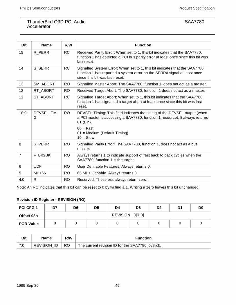
ThunderBird Q3D PCI Audio SAA7780Accelerator
Philips Semiconductors Product Specification
1999 Sep 30 48
Status Register - STATUS (RO/RW)
STEP-PING
PERR_
RESP
SNOOP_ENB
MEM_
INV_EN
SPEC_
CNTL
MAST_
CNTL
MEM_
CNTL
IO_
CNTL
POR Value 0 0 0 0 0 0 0 0
Bit Name R/W Function
15:10 R RO Reserved. These bits always return zero.
9 FBACK_ENB RO Fast Back-to-Back Enable: the SAA7780, function 1 does not support fast back to back master cycles therefore this bit always returns a zero.
8 SERR_RESP RW System Error Response: When set to 1, the SAA7780, function 1 responds to detected PCI bus address parity errors by asserting SERR#. When 0, the SAA7780 ignores these errors.
7 STEPPING RO Address / Data Stepping: Always returns 0.
6 PERR_RESP RW Parity Error Response: When set to 1, the SAA7780, function 1 responds to detected PCI bus data parity errors by asserting PERR#. When 0, the SAA7780 ignores PCI bus data parity errors.
5 SNOOP_ENB RO VGA Snoop Enable. The SAA7780, function 1 does not support VGA snoop enable, therefor this bit always returns a zero.
4 MEM_INV_EN RO Memory Write and Invalidate Enable: Always returns 0.
3 SPEC_CNTL RO Special Cycle Control: Controls the devices ability to respond to Special Cycle Operations. A value of 0 causes the SAA7780, function 1 to ignore all Special Cycles.
2 MAST_CNTL RO Master Control: The SAA7780, function 1 does not have any master functions.
1 MEM_CNTL RO Memory Response Control: The SAA7780, function 1 does not support target memory cycles therefore this bit always returns a zero.
0 IO_CNTL RW I/O Response Control: Controls the SAA7780, function 1’s response to I/O space. A value of 0 disables the device response. A value of 1 allows the device to respond to I/O space accesses.
PCI CFG 1 D15 D14 D13 D12 D11 D10 D9 D8
Offset 06hR_PERR S_SERR SM_
ABORT
RT_
ABORT
ST_
ABORT
DEVSEL_TMG S_PERR
POR Value 0 0 0 0 0 0 1 0
D7 D6 D5 D4 D3 D2 D1 D0
F_
BK2BK
UDF MHz66 R R R R R
POR Value 1 0 0 0 0 0 0 0

ThunderBird Q3D PCI Audio SAA7780Accelerator
Philips Semiconductors Product Specification
1999 Sep 30 49
Note: An RC indicates that this bit can be reset to 0 by writing a 1. Writing a zero leaves this bit unchanged.
Revision ID Register - REVISION (RO)
Bit Name R/W Function
15 R_PERR RC Received Parity Error: When set to 1, this bit indicates that the SAA7780, function 1 has detected a PCI bus parity error at least once since this bit was last reset.
14 S_SERR RC Signalled System Error: When set to 1, this bit indicates that the SAA7780, function 1 has reported a system error on the SERR# signal at least once since this bit was last reset.
13 SM_ABORT RO Signalled Master Abort: The SAA7780, function 1, does not act as a master.
12 RT_ABORT RO Received Target Abort: The SAA7780, function 1 does not act as a master.
11 ST_ABORT RC Signalled Target Abort: When set to 1, this bit indicates that the SAA7780, function 1 has signalled a target abort at least once since this bit was last reset.
10:9 DEVSEL_TMG
RO DEVSEL Timing: This field indicates the timing of the DEVSEL output (when a PCI master is accessing a SAA7780, function 1 resource). It always returns 01 (Bin).
00 = Fast01 = Medium (Default Timing)10 = Slow
8 S_PERR RO Signalled Parity Error: The SAA7780, function 1, does not act as a bus master.
7 F_BK2BK RO Always returns 1 to indicate support of fast back to back cycles when the SAA7780, function 1 is the target.
6 UDF RO User Definable Features. Always returns 0.
5 MHz66 RO 66 MHz Capable. Always returns 0.
4:0 R RO Reserved. These bits always return zero.
PCI CFG 1 D7 D6 D5 D4 D3 D2 D1 D0
Offset 08h REVISION_ID[7:0]
POR Value 0 0 0 0 0 0 0 0
Bit Name R/W Function
7:0 REVISION_ID RO The current revision ID for the SAA7780 joystick.
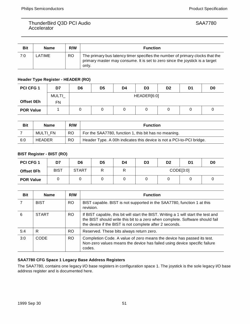
ThunderBird Q3D PCI Audio SAA7780Accelerator
Philips Semiconductors Product Specification
1999 Sep 30 50
Class Code Register - CLASS (RO)
CACHELINE Size Register - CACHELINE (RO)
Master Latency Timer Register - LATIME (RW)
PCI CFG 1 D23 D22 D21 D20 D19 D18 D17 D16
Offset 09h BASE_CLASS[7:0]
POR Value 0 0 0 0 1 0 0 1
D15 D14 D13 D12 D11 D10 D9 D8
SUB_CLASS[7:0]
POR Value 1 0 0 0 0 0 0 0
D7 D6 D5 D4 D3 D2 D1 D0
PGM_IFACE[7:0]
POR Value 0 0 0 0 0 0 0 0
Bit Name R/W Function
23:16 BASE_CLASS RO The base class of 09h describes an input device.
15:8 SUB_CLASS RO The sub class of 80h describes a “other” input controller.
7:0 PGM_IFACE RO Device generic function identification.
PCI CFG 1 D7 D6 D5 D4 D3 D2 D1 D0
Offset 0Ch CACHELINE[7:0]
POR Value 0 0 0 0 0 0 0 0
Bit Name R/W Function
7:0 CACHELINE RO Reserved for cache line size indicator.
PCI CFG 1 D7 D6 D5 D4 D3 D2 D1 D0
Offset 0Dh LATIME[7:0]
POR Value 0 0 0 0 0 0 0 0
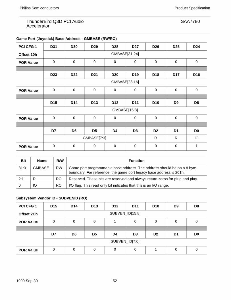
ThunderBird Q3D PCI Audio SAA7780Accelerator
Philips Semiconductors Product Specification
1999 Sep 30 51
Header Type Register - HEADER (RO)
BIST Register - BIST (RO)
SAA7780 CFG Space 1 Legacy Base Address RegistersThe SAA7780, contains one legacy I/O base registers in configuration space 1. The joystick is the sole legacy I/O base address register and is documented here.
Bit Name R/W Function
7:0 LATIME RO The primary bus latency timer specifies the number of primary clocks that the primary master may consume. It is set to zero since the joystick is a target only.
PCI CFG 1 D7 D6 D5 D4 D3 D2 D1 D0
Offset 0EhMULTI_
FN
HEADER[6:0]
POR Value 1 0 0 0 0 0 0 0
Bit Name R/W Function
7 MULTI_FN RO For the SAA7780, function 1, this bit has no meaning.
6:0 HEADER RO Header Type. A 00h indicates this device is not a PCI-to-PCI bridge.
PCI CFG 1 D7 D6 D5 D4 D3 D2 D1 D0
Offset 0Fh BIST START R R CODE[3:0]
POR Value 0 0 0 0 0 0 0 0
Bit Name R/W Function
7 BIST RO BIST capable. BIST is not supported in the SAA7780, function 1 at this revision.
6 START RO If BIST capable, this bit will start the BIST. Writing a 1 will start the test and the BIST should write this bit to a zero when complete. Software should fail the device if the BIST is not complete after 2 seconds.
5:4 R RO Reserved. These bits always return zero.
3:0 CODE RO Completion Code. A value of zero means the device has passed its test. Non-zero values means the device has failed using device specific failure codes.
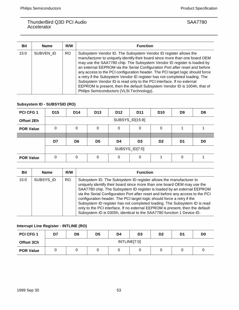
ThunderBird Q3D PCI Audio SAA7780Accelerator
Philips Semiconductors Product Specification
1999 Sep 30 52
Game Port (Joystick) Base Address - GMBASE (RW/RO)
Subsystem Vendor ID - SUBVENID (RO)
PCI CFG 1 D31 D30 D29 D28 D27 D26 D25 D24
Offset 10h GMBASE[31:24]
POR Value 0 0 0 0 0 0 0 0
D23 D22 D21 D20 D19 D18 D17 D16
GMBASE[23:16]
POR Value 0 0 0 0 0 0 0 0
D15 D14 D13 D12 D11 D10 D9 D8
GMBASE[15:8]
POR Value 0 0 0 0 0 0 0 0
D7 D6 D5 D4 D3 D2 D1 D0
GMBASE[7:3] R R IO
POR Value 0 0 0 0 0 0 0 1
Bit Name R/W Function
31:3 GMBASE RW Game port programmable base address. The address should be on a 8 byte boundary. For reference, the game port legacy base address is 201h.
2:1 R RO Reserved. These bits are reserved and always return zeros for plug and play.
0 IO RO I/O flag. This read only bit indicates that this is an I/O range.
PCI CFG 1 D15 D14 D13 D12 D11 D10 D9 D8
Offset 2Ch SUBVEN_ID[15:8]
POR Value 0 0 0 1 0 0 0 0
D7 D6 D5 D4 D3 D2 D1 D0
SUBVEN_ID[7:0]
POR Value 0 0 0 0 0 1 0 0
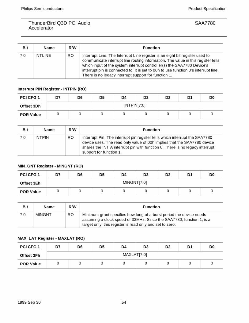
ThunderBird Q3D PCI Audio SAA7780Accelerator
Philips Semiconductors Product Specification
1999 Sep 30 53
Subsystem ID - SUBSYSID (RO)
Interrupt Line Register - INTLINE (RO)
Bit Name R/W Function
15:0 SUBVEN_ID RO Subsystem Vendor ID. The Subsystem Vendor ID register allows the manufacturer to uniquely identify their board since more than one board OEM may use the SAA7780 chip. The Subsystem Vendor ID register is loaded by an external EEPROM via the Serial Configuration Port after reset and before any access to the PCI configuration header. The PCI target logic should force a retry if the Subsystem Vendor ID register has not completed loading. The Subsystem Vendor ID is read only to the PCI interface. If no external EEPROM is present, then the default Subsystem Vendor ID is 1004h, that of Philips Semiconductors (VLSI Technology).
PCI CFG 1 D15 D14 D13 D12 D11 D10 D9 D8
Offset 2Eh SUBSYS_ID[15:8]
POR Value 0 0 0 0 0 0 1 1
D7 D6 D5 D4 D3 D2 D1 D0
SUBSYS_ID[7:0]
POR Value 0 0 0 0 0 1 0 1
Bit Name R/W Function
15:0 SUBSYS_ID RO Subsystem ID. The Subsystem ID register allows the manufacturer to uniquely identify their board since more than one board OEM may use the SAA7780 chip. The Subsystem ID register is loaded by an external EEPROM via the Serial Configuration Port after reset and before any access to the PCI configuration header. The PCI target logic should force a retry if the Subsystem ID register has not completed loading. The Subsystem ID is read only to the PCI interface. If no external EEPROM is present, then the default Subsystem ID is 0305h, identical to the SAA7780 function 1 Device ID.
PCI CFG 1 D7 D6 D5 D4 D3 D2 D1 D0
Offset 3Ch INTLINE[7:0]
POR Value 0 0 0 0 0 0 0 0
ThunderBird Q3D PCI Audio SAA7780Accelerator
Philips Semiconductors Product Specification
1999 Sep 30 54
Interrupt PIN Register - INTPIN (RO)
MIN_GNT Register - MINGNT (RO)
MAX_LAT Register - MAXLAT (RO)
Bit Name R/W Function
7:0 INTLINE RO Interrupt Line. The Interrupt Line register is an eight bit register used to communicate interrupt line routing information. The value in this register tells which input of the system interrupt controller(s) the SAA7780 Device's interrupt pin is connected to. It is set to 00h to use function 0’s interrupt line. There is no legacy interrupt support for function 1.
PCI CFG 1 D7 D6 D5 D4 D3 D2 D1 D0
Offset 3Dh INTPIN[7:0]
POR Value 0 0 0 0 0 0 0 0
Bit Name R/W Function
7:0 INTPIN RO Interrupt Pin. The interrupt pin register tells which interrupt the SAA7780 device uses. The read only value of 00h implies that the SAA7780 device shares the INT A interrupt pin with function 0. There is no legacy interrupt support for function 1.
PCI CFG 1 D7 D6 D5 D4 D3 D2 D1 D0
Offset 3Eh MINGNT[7:0]
POR Value 0 0 0 0 0 0 0 0
Bit Name R/W Function
7:0 MINGNT RO Minimum grant specifies how long of a burst period the device needs assuming a clock speed of 33MHz. Since the SAA7780, function 1, is a target only, this register is read only and set to zero.
PCI CFG 1 D7 D6 D5 D4 D3 D2 D1 D0
Offset 3Fh MAXLAT[7:0]
POR Value 0 0 0 0 0 0 0 0
ThunderBird Q3D PCI Audio SAA7780Accelerator
Philips Semiconductors Product Specification
1999 Sep 30 55
PCI Configuration Space 2 The following table is a summary of all the PCI configuration space registers. The registers that are block-mates with the PCI interface (offset 00h - 3Ch) will be detailed following this table. The remainder of the registers will be detailed with the blocks they control. This register space is for the 16650 UART.
PCI Configuration Space 2 Register Map
Vendor ID Register - VENDOR_ID (RO)
Bit Name R/W Function
7:0 MAXLAT RO Maximum latency specifies how often a device needs to gain access to the PCI bus. The SAA7780, function 1, is a target only, this register is read only and set to zero.
Byte 3 Byte 2 Byte 1 Byte 0 OffsetDevice ID Vendor ID 00h
Status Command 04hClass Code Revision ID 08h
BIST Header Type Master Latency Timer Cache Line Size 0Ch
UARTBASE 10-13hReserved 14-2B
Subsystem ID Subsystem Vendor ID 2Ch
Reserved 30-3BhMax_Lat Min_Gnt Interrupt Pin Interrupt Line 3Ch
Reserved Reserved Reserved UARTCFG0 40hReserved Reserved Reserved SFCR 44h
Reserved 48-FFh
PCI CFG 2 D15 D14 D13 D12 D11 D10 D9 D8
Offset 00h VENDOR_ID[15:8]
POR Value 0 0 0 1 0 0 0 0
D7 D6 D5 D4 D3 D2 D1 D0
VENDOR_ID[7:0]
POR Value 0 0 0 0 0 1 0 0
Bit Name R/W Function
15:0 VENDOR_ID RO The PCI Vendor ID for Philips Semiconductors (VLSI Technology) is 1004h.
ThunderBird Q3D PCI Audio SAA7780Accelerator
Philips Semiconductors Product Specification
1999 Sep 30 56
Device ID Register - DEVICE_ID (RO)
Command Register - COMMAND (RO/RW)
PCI CFG 2 D15 D14 D13 D12 D11 D10 D9 D8
Offset 02h DEVICE_ID[15:8]
POR Value 0 0 0 0 0 0 1 1
D7 D6 D5 D4 D3 D2 D1 D0
DEVICE_ID[7:0]
POR Value 0 0 0 0 0 1 1 0
Bit Name R/W Function
15:0 DEVICE_ID RO The Device ID for the SAA7780, function 2 is 0306h.
PCI CFG 2 D15 D14 D13 D12 D11 D10 D9 D8
Offset 04hR R R R R R FBACK_
ENBSERR_R
ESP
POR Value 0 0 0 0 0 0 0 0
D7 D6 D5 D4 D3 D2 D1 D0
STEP-PING
PERR_
RESP
SNOOP_ENB
MEM_
INV_EN
SPEC_
CNTL
MAST_
CNTL
MEM_
CNTL
IO_
CNTL
POR Value 0 0 0 0 0 0 0 0
Bit Name R/W Function
15:10 R RO Reserved. These bits always return zero.
9 FBACK_ENB RO Fast Back-to-Back Enable: the SAA7780, function 2 does not support fast back to back master cycles therefore this bit always returns a zero.
8 SERR_RESP RW System Error Response: When set to 1, the SAA7780, function 2 responds to detected PCI bus address parity errors by asserting SERR#. When 0, the SAA7780 ignores these errors.
7 STEPPING RO Address / Data Stepping: Always returns 0.
6 PERR_RESP RW Parity Error Response: When set to 1, the SAA7780, function 2 responds to detected PCI bus data parity errors by asserting PERR#. When 0, the SAA7780 ignores PCI bus data parity errors.
5 SNOOP_ENB RO VGA Snoop Enable. The SAA7780, function 2 does not support VGA snoop enable, therefor this bit always returns a zero.
ThunderBird Q3D PCI Audio SAA7780Accelerator
Philips Semiconductors Product Specification
1999 Sep 30 57
Status Register - STATUS (RO/RW)
4 MEM_INV_EN RO Memory Write and Invalidate Enable: Always returns 0.
3 SPEC_CNTL RO Special Cycle Control: Controls the devices ability to respond to Special Cycle Operations. A value of 0 causes the SAA7780, function 2 to ignore all Special Cycles.
2 MAST_CNTL RO Master Control: The SAA7780, function 2 does not have any master functions.
1 MEM_CNTL RO Memory Response Control: The SAA7780, function 2 does not support target memory cycles therefore this bit always returns a zero.
0 IO_CNTL RW I/O Response Control: Controls the SAA7780, function 2’s response to I/O space. A value of 0 disables the device response. A value of 1 allows the device to respond to I/O space accesses.
PCI CFG 2 D15 D14 D13 D12 D11 D10 D9 D8
Offset 06hR_PERR S_SERR SM_
ABORT
RT_
ABORT
ST_
ABORT
DEVSEL_TMG S_PERR
POR Value 0 0 0 0 0 0 1 0
D7 D6 D5 D4 D3 D2 D1 D0
F_
BK2BK
UDF MHz66 R R R R R
POR Value 1 0 0 0 0 0 0 0
Bit Name R/W Function
15 R_PERR RC Received Parity Error: When set to 1, this bit indicates that the SAA7780, function 2 has detected a PCI bus parity error at least once since this bit was last reset.
14 S_SERR RC Signalled System Error: When set to 1, this bit indicates that the SAA7780, function 2 has reported a system error on the SERR# signal at least once since this bit was last reset.
13 SM_ABORT RO Signalled Master Abort: The SAA7780, function 2, does not act as a master.
12 RT_ABORT RO Received Target Abort: The SAA7780, function 2 does not act as a master.
11 ST_ABORT RC Signalled Target Abort: When set to 1, this bit indicates that the SAA7780, function 2 has signalled a target abort at least once since this bit was last reset.
Bit Name R/W Function
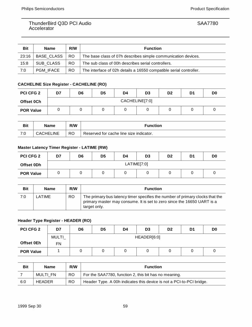
ThunderBird Q3D PCI Audio SAA7780Accelerator
Philips Semiconductors Product Specification
1999 Sep 30 58
Note: An RC indicates that this bit can be reset to 0 by writing a 1. Writing a zero leaves this bit unchanged.
Revision ID Register - REVISION (RO)
Class Code Register - CLASS (RO)
10:9 DEVSEL_TMG
RO DEVSEL Timing: This field indicates the timing of the DEVSEL output (when a PCI master is accessing a SAA7780 resource). It always returns 01 (Bin).
00 = Fast01 = Medium (Default Timing)10 = Slow
8 S_PERR RO Signalled Parity Error: The SAA7780, function 2, does not act as a bus master.
7 F_BK2BK RO Always returns 1 to indicate support of fast back to back cycles when the SAA7780, function 2 is the target.
6 UDF RO User Definable Features. Always returns 0.
5 MHz66 RO 66 MHz Capable. Always returns 0.
4:0 R RO Reserved. These bits always return zero.
PCI CFG 2 D7 D6 D5 D4 D3 D2 D1 D0
Offset 08h REVISION_ID[7:0]
POR Value 0 0 0 0 0 0 0 0
Bit Name R/W Function
7:0 REVISION_ID RO The current revision ID for the SAA7780, function 2 joystick.
PCI CFG 2 D23 D22 D21 D20 D19 D18 D17 D16
Offset 09h BASE_CLASS[7:0]
POR Value 0 0 0 0 0 1 1 1
D15 D14 D13 D12 D11 D10 D9 D8
SUB_CLASS[7:0]
POR Value 0 0 0 0 0 0 0 0
D7 D6 D5 D4 D3 D2 D1 D0
PGM_IFACE[7:0]
POR Value 0 0 0 0 0 0 1 0
Bit Name R/W Function
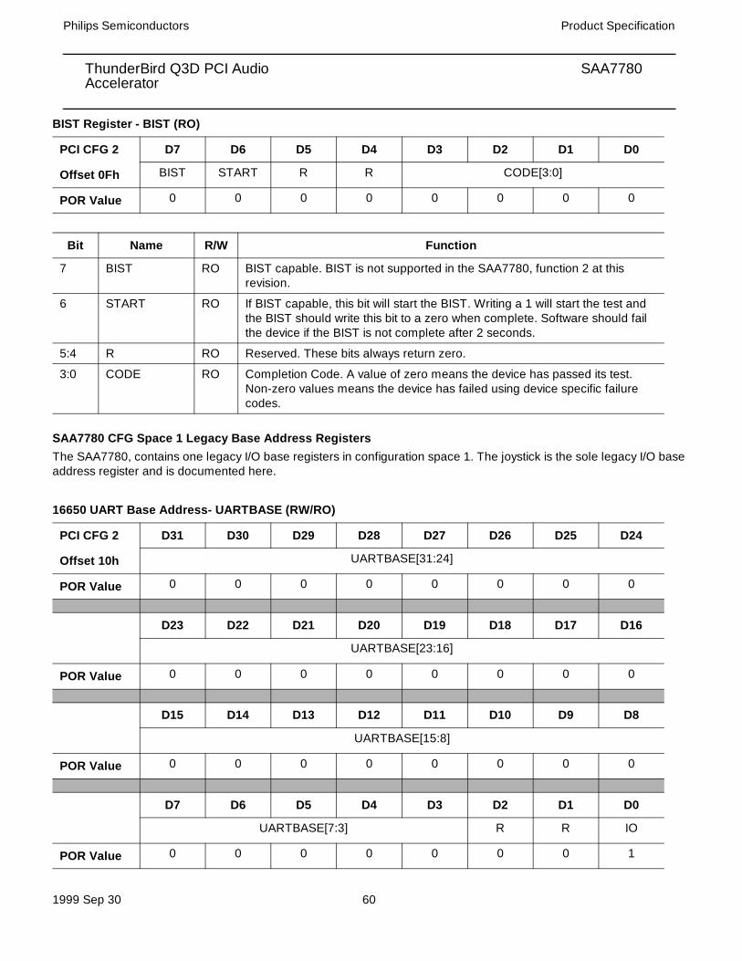
ThunderBird Q3D PCI Audio SAA7780Accelerator
Philips Semiconductors Product Specification
1999 Sep 30 59
CACHELINE Size Register - CACHELINE (RO)
Master Latency Timer Register - LATIME (RW)
Header Type Register - HEADER (RO)
Bit Name R/W Function
23:16 BASE_CLASS RO The base class of 07h describes simple communication devices.
15:8 SUB_CLASS RO The sub class of 00h describes serial controllers.
7:0 PGM_IFACE RO The interface of 02h details a 16550 compatible serial controller.
PCI CFG 2 D7 D6 D5 D4 D3 D2 D1 D0
Offset 0Ch CACHELINE[7:0]
POR Value 0 0 0 0 0 0 0 0
Bit Name R/W Function
7:0 CACHELINE RO Reserved for cache line size indicator.
PCI CFG 2 D7 D6 D5 D4 D3 D2 D1 D0
Offset 0Dh LATIME[7:0]
POR Value 0 0 0 0 0 0 0 0
Bit Name R/W Function
7:0 LATIME RO The primary bus latency timer specifies the number of primary clocks that the primary master may consume. It is set to zero since the 16650 UART is a target only.
PCI CFG 2 D7 D6 D5 D4 D3 D2 D1 D0
Offset 0EhMULTI_
FN
HEADER[6:0]
POR Value 1 0 0 0 0 0 0 0
Bit Name R/W Function
7 MULTI_FN RO For the SAA7780, function 2, this bit has no meaning.
6:0 HEADER RO Header Type. A 00h indicates this device is not a PCI-to-PCI bridge.
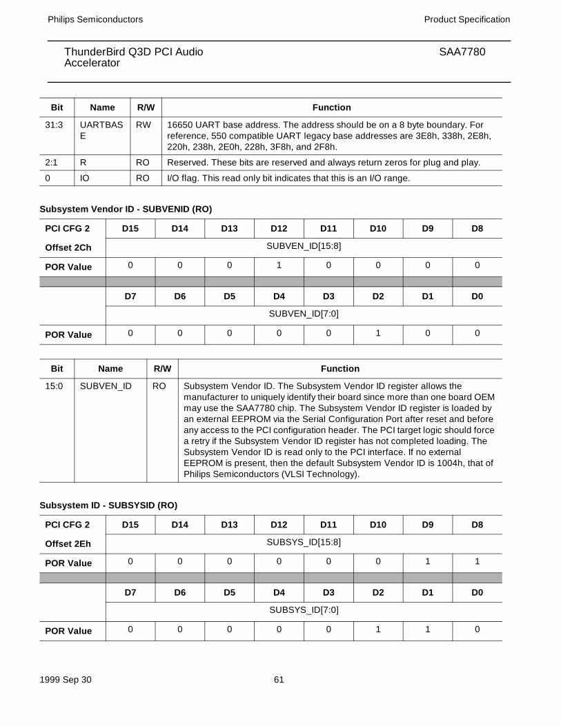
ThunderBird Q3D PCI Audio SAA7780Accelerator
Philips Semiconductors Product Specification
1999 Sep 30 60
BIST Register - BIST (RO)
SAA7780 CFG Space 1 Legacy Base Address RegistersThe SAA7780, contains one legacy I/O base registers in configuration space 1. The joystick is the sole legacy I/O base address register and is documented here.
16650 UART Base Address- UARTBASE (RW/RO)
PCI CFG 2 D7 D6 D5 D4 D3 D2 D1 D0
Offset 0Fh BIST START R R CODE[3:0]
POR Value 0 0 0 0 0 0 0 0
Bit Name R/W Function
7 BIST RO BIST capable. BIST is not supported in the SAA7780, function 2 at this revision.
6 START RO If BIST capable, this bit will start the BIST. Writing a 1 will start the test and the BIST should write this bit to a zero when complete. Software should fail the device if the BIST is not complete after 2 seconds.
5:4 R RO Reserved. These bits always return zero.
3:0 CODE RO Completion Code. A value of zero means the device has passed its test. Non-zero values means the device has failed using device specific failure codes.
PCI CFG 2 D31 D30 D29 D28 D27 D26 D25 D24
Offset 10h UARTBASE[31:24]
POR Value 0 0 0 0 0 0 0 0
D23 D22 D21 D20 D19 D18 D17 D16
UARTBASE[23:16]
POR Value 0 0 0 0 0 0 0 0
D15 D14 D13 D12 D11 D10 D9 D8
UARTBASE[15:8]
POR Value 0 0 0 0 0 0 0 0
D7 D6 D5 D4 D3 D2 D1 D0
UARTBASE[7:3] R R IO
POR Value 0 0 0 0 0 0 0 1
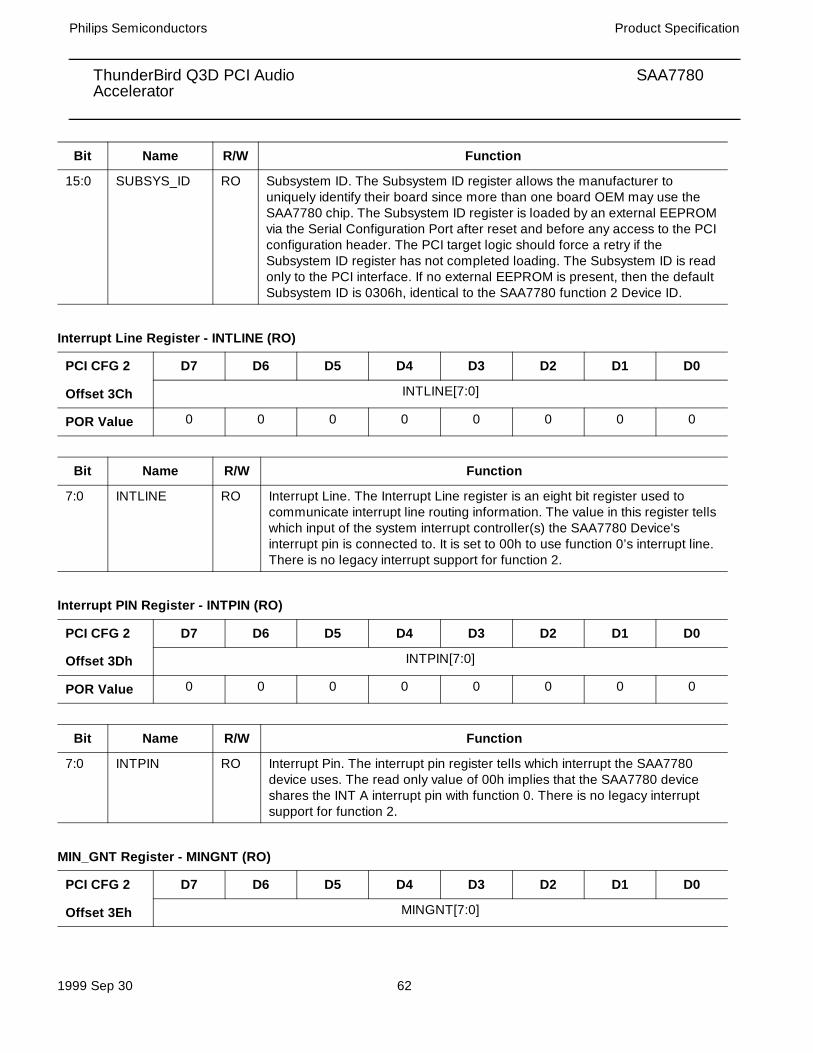
ThunderBird Q3D PCI Audio SAA7780Accelerator
Philips Semiconductors Product Specification
1999 Sep 30 61
Subsystem Vendor ID - SUBVENID (RO)
Subsystem ID - SUBSYSID (RO)
Bit Name R/W Function
31:3 UARTBASE
RW 16650 UART base address. The address should be on a 8 byte boundary. For reference, 550 compatible UART legacy base addresses are 3E8h, 338h, 2E8h, 220h, 238h, 2E0h, 228h, 3F8h, and 2F8h.
2:1 R RO Reserved. These bits are reserved and always return zeros for plug and play.
0 IO RO I/O flag. This read only bit indicates that this is an I/O range.
PCI CFG 2 D15 D14 D13 D12 D11 D10 D9 D8
Offset 2Ch SUBVEN_ID[15:8]
POR Value 0 0 0 1 0 0 0 0
D7 D6 D5 D4 D3 D2 D1 D0
SUBVEN_ID[7:0]
POR Value 0 0 0 0 0 1 0 0
Bit Name R/W Function
15:0 SUBVEN_ID RO Subsystem Vendor ID. The Subsystem Vendor ID register allows the manufacturer to uniquely identify their board since more than one board OEM may use the SAA7780 chip. The Subsystem Vendor ID register is loaded by an external EEPROM via the Serial Configuration Port after reset and before any access to the PCI configuration header. The PCI target logic should force a retry if the Subsystem Vendor ID register has not completed loading. The Subsystem Vendor ID is read only to the PCI interface. If no external EEPROM is present, then the default Subsystem Vendor ID is 1004h, that of Philips Semiconductors (VLSI Technology).
PCI CFG 2 D15 D14 D13 D12 D11 D10 D9 D8
Offset 2Eh SUBSYS_ID[15:8]
POR Value 0 0 0 0 0 0 1 1
D7 D6 D5 D4 D3 D2 D1 D0
SUBSYS_ID[7:0]
POR Value 0 0 0 0 0 1 1 0
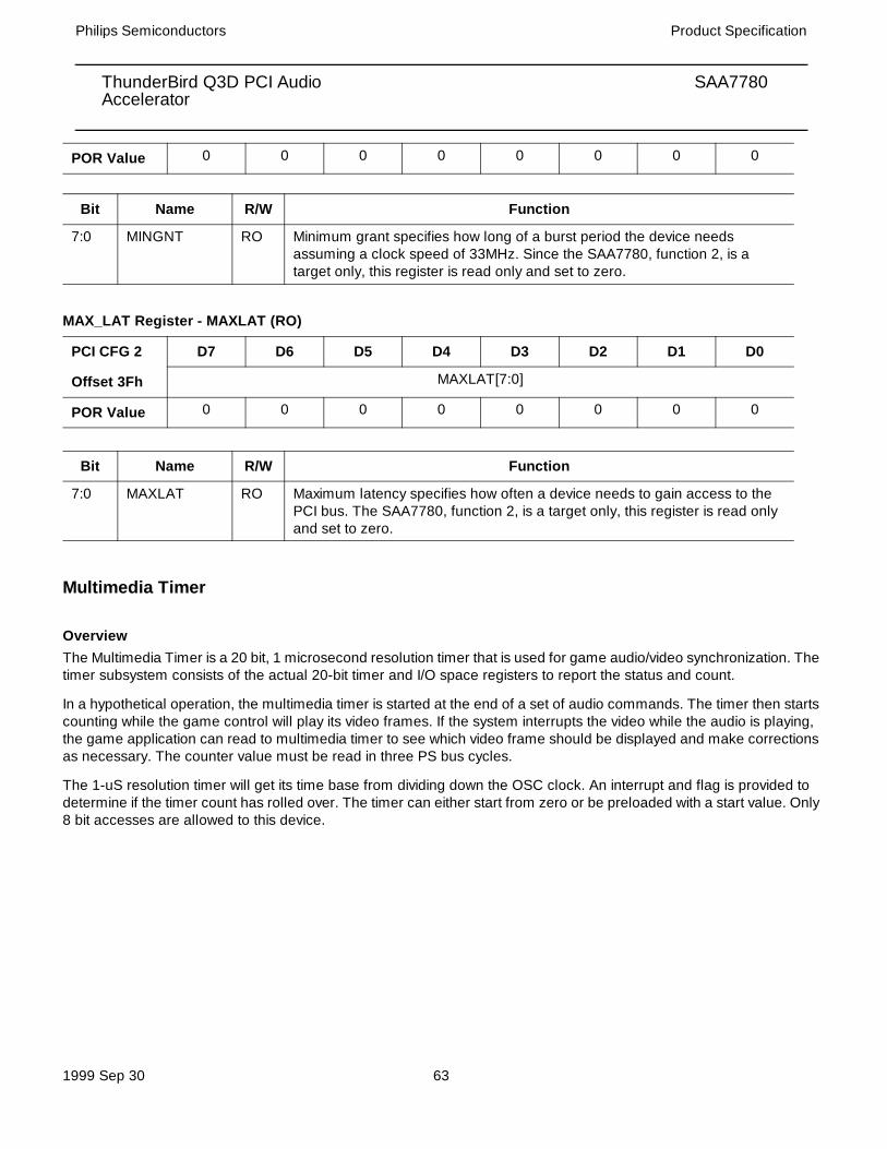
ThunderBird Q3D PCI Audio SAA7780Accelerator
Philips Semiconductors Product Specification
1999 Sep 30 62
Interrupt Line Register - INTLINE (RO)
Interrupt PIN Register - INTPIN (RO)
MIN_GNT Register - MINGNT (RO)
Bit Name R/W Function
15:0 SUBSYS_ID RO Subsystem ID. The Subsystem ID register allows the manufacturer to uniquely identify their board since more than one board OEM may use the SAA7780 chip. The Subsystem ID register is loaded by an external EEPROM via the Serial Configuration Port after reset and before any access to the PCI configuration header. The PCI target logic should force a retry if the Subsystem ID register has not completed loading. The Subsystem ID is read only to the PCI interface. If no external EEPROM is present, then the default Subsystem ID is 0306h, identical to the SAA7780 function 2 Device ID.
PCI CFG 2 D7 D6 D5 D4 D3 D2 D1 D0
Offset 3Ch INTLINE[7:0]
POR Value 0 0 0 0 0 0 0 0
Bit Name R/W Function
7:0 INTLINE RO Interrupt Line. The Interrupt Line register is an eight bit register used to communicate interrupt line routing information. The value in this register tells which input of the system interrupt controller(s) the SAA7780 Device's interrupt pin is connected to. It is set to 00h to use function 0’s interrupt line. There is no legacy interrupt support for function 2.
PCI CFG 2 D7 D6 D5 D4 D3 D2 D1 D0
Offset 3Dh INTPIN[7:0]
POR Value 0 0 0 0 0 0 0 0
Bit Name R/W Function
7:0 INTPIN RO Interrupt Pin. The interrupt pin register tells which interrupt the SAA7780 device uses. The read only value of 00h implies that the SAA7780 device shares the INT A interrupt pin with function 0. There is no legacy interrupt support for function 2.
PCI CFG 2 D7 D6 D5 D4 D3 D2 D1 D0
Offset 3Eh MINGNT[7:0]
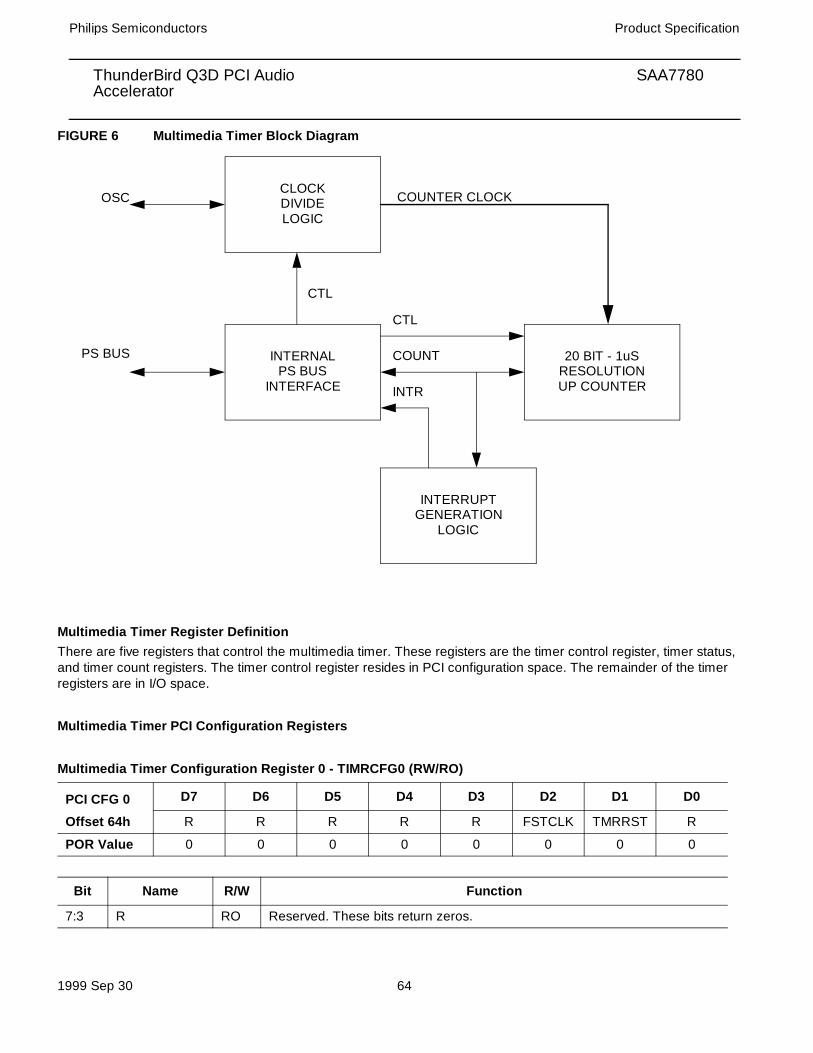
ThunderBird Q3D PCI Audio SAA7780Accelerator
Philips Semiconductors Product Specification
1999 Sep 30 63
MAX_LAT Register - MAXLAT (RO)
Multimedia Timer
OverviewThe Multimedia Timer is a 20 bit, 1 microsecond resolution timer that is used for game audio/video synchronization. The timer subsystem consists of the actual 20-bit timer and I/O space registers to report the status and count.
In a hypothetical operation, the multimedia timer is started at the end of a set of audio commands. The timer then starts counting while the game control will play its video frames. If the system interrupts the video while the audio is playing, the game application can read to multimedia timer to see which video frame should be displayed and make corrections as necessary. The counter value must be read in three PS bus cycles.
The 1-uS resolution timer will get its time base from dividing down the OSC clock. An interrupt and flag is provided to determine if the timer count has rolled over. The timer can either start from zero or be preloaded with a start value. Only 8 bit accesses are allowed to this device.
POR Value 0 0 0 0 0 0 0 0
Bit Name R/W Function
7:0 MINGNT RO Minimum grant specifies how long of a burst period the device needs assuming a clock speed of 33MHz. Since the SAA7780, function 2, is a target only, this register is read only and set to zero.
PCI CFG 2 D7 D6 D5 D4 D3 D2 D1 D0
Offset 3Fh MAXLAT[7:0]
POR Value 0 0 0 0 0 0 0 0
Bit Name R/W Function
7:0 MAXLAT RO Maximum latency specifies how often a device needs to gain access to the PCI bus. The SAA7780, function 2, is a target only, this register is read only and set to zero.
ThunderBird Q3D PCI Audio SAA7780Accelerator
Philips Semiconductors Product Specification
1999 Sep 30 64
FIGURE 6 Multimedia Timer Block Diagram
Multimedia Timer Register DefinitionThere are five registers that control the multimedia timer. These registers are the timer control register, timer status, and timer count registers. The timer control register resides in PCI configuration space. The remainder of the timer registers are in I/O space.
Multimedia Timer PCI Configuration Registers
Multimedia Timer Configuration Register 0 - TIMRCFG0 (RW/RO)
PCI CFG 0 D7 D6 D5 D4 D3 D2 D1 D0
Offset 64h R R R R R FSTCLK TMRRST R
POR Value 0 0 0 0 0 0 0 0
Bit Name R/W Function
7:3 R RO Reserved. These bits return zeros.
PS BUS
CLOCKDIVIDELOGIC
OSC
CTL
INTERNALPS BUS
INTERFACE
INTERRUPTGENERATION
LOGIC
20 BIT - 1uSRESOLUTIONUP COUNTER
CTL
COUNT
INTR
COUNTER CLOCK
ThunderBird Q3D PCI Audio SAA7780Accelerator
Philips Semiconductors Product Specification
1999 Sep 30 65
Multimedia Timer I/O Space Registers
Multimedia Timer Status Register - TMSTAT (RW/RO)
Multimedia Timer Count Registers There are three registers required to hold the timer value. These three registers can be read at different cycles, It is recommended that the least significant byte be read first for the most accuracy.
Multimedia Timer Count Register 2 - TMCOUNT2 (RW/RO)
2 FSTCLK RW Fast clock enable. When set, the timer counter will use the PCI clock instead of the 1 micro second timer clock. This function will reduce the simulation and test time of the timer.
1 TMRRST RW Timer reset. When set, this bit holds the multimedia timer in reset. The multimedia timer is also reset by the system reset.
0 R RO Reserved. This bit returns a zero.
SONGBASE D7 D6 D5 D4 D3 D2 D1 D0
Offset 00hR R R R TPLD TRE-
SUMETMINT TINTEN
POR Value 0 0 0 0 0 0 0 0
Bit Name R/W Function
7:4 R RO Reserved. These bits return zeros.
3 TPLD RW Timer preload indicator. When set, this indicates the timer will start counting from the values set in the timer count registers. When cleared, the timer will start counting from zero or its last value when stopped
2 TRESUME RW Timer resume. When set, the timer will resume counting at the next 1uS clock edge. When cleared, the timer will stop counting.
1 TMINT RC Timer interrupt. When asserted, the multimedia timer has flagged an interrupt when the timer has counted to zero. The timer will continue to count. Writing a one to this bit will clear the interrupt.
0 TINTEN RW Timer interrupt enable. When set, the multimedia timer will generate an interrupt.
SONGBASE D7 D6 D5 D4 D3 D2 D1 D0
Offset 03h R R R R TMCOUNT2[7:0]
POR Value 0 0 0 0 0 0 0 0
Bit Name R/W Function
ThunderBird Q3D PCI Audio SAA7780Accelerator
Philips Semiconductors Product Specification
1999 Sep 30 66
Multimedia Timer Count Register 1 - TMCOUNT1 (RW)
Multimedia Timer Count Register 0 - TMCOUNT0 (RW)
Bit Name R/W Function
7:4 R RO Reserved. These bits return zeros.
3:0 TMCOUNT2 RW High nibble timer count. This nibble is the most significant digits of the timer value.
SONGBASE D7 D6 D5 D4 D3 D2 D1 D0
Offset 02h TMCOUNT1[7:0]
POR Value 0 0 0 0 0 0 0 0
Bit Name R/W Function
7:0 TMCOUNT1 RW Middle byte timer count. This byte is the middle significant digits of the timer value.
SONGBASE D7 D6 D5 D4 D3 D2 D1 D0
Offset 01h TMCOUNT0[7:0]
POR Value 0 0 0 0 0 0 0 0
Bit Name R/W Function
7:0 TMCOUNT0 RW Low byte timer count. This byte is the least significant digits of the timer value.
ThunderBird Q3D PCI Audio SAA7780Accelerator
Philips Semiconductors Product Specification
1999 Sep 30 67
Absolute Maximum Ratings Absolute maximum ratings are those values which damage to the device may occur. Functional operation under these conditions or at any other condition beyond those indicated in the operational sections of this specification is not implied.1
Power Supply Operating Requirements
SAA7780 Minimum VDD Operating RequirementIMPORTANT: The SAA7780 requires VDD >= 3.0V. If VDD < 3.0V, excessive damage from hot electrons might occur.
SAA7780 Power Supply Sequencing Requirement0 <= (NWELL - VDD) < 4.0V
IMPORTANT: The 5.0V (NWELL) supply must power up ahead of the 3.3V (VDD, not VDDIC) supply. Likewise, the 3.0V supply must power down before the 5.0V supply. More specifically, the voltage level of the 5.0V supply must always exceed, or at least equal, the voltage level of the 3.3V supply during power up or down, but not by more than 4.0V. This is due the biasing of the P+ source junctions and that some pad gate oxides see the (NWELL-VDD) voltage level. If this level exceeds 4.0V or becomes less than 0V, damage will occur.
Device Maximum Ratings The following table notes both the operating and non-operating conditions for both the 3.0V and 5.0V tolerant pads. Remember that the ranges imply an operating range unless otherwise noted. The 5.0V tolerant pads signal at 3.0V levels and are CMOS and TTL compatible.
Device Maximum Ratings
1. Adapted from the JEDEC standards JESD8-A and JESD36.
Condition Symbol Maximum Ratings
Ambient Operating Temperature TA 0°C to +70°CAmbient Storage Temperature TS -65°C to +150°CNon-Operating Core and Ring Supply Voltage VDD, VDDIC -0.5V to 4.6V *
Operating Core Supply Voltage VDDIC -0.5V to 3.63V *
Operating Ring Supply Voltage VDD 3.0V to 3.63V *
5V Tolerant Supply (5.0V nominal supply) NWELL -0.5V to 5.5V *
NWELL to VDD Differential NWELL-VDD 0 ≤ (NWELL-VDD) < 4.0V
3V Tolerant I/O DC Input Voltage VI3 -0.5V to VDD+0.5V (≤ 4.6V max)+
3V Tolerant I/O DC Output Voltage VO3 -0.5V to VDD+0.5V (≤ 4.6V max)+
5V Tolerant I/O DC Input Voltage VI5 -0.5V to 5.5V (≤ 6.0V max)+
5V Tolerant I/O DC Output Voltage VO5 -0.5V to VDD+0.5V (≤ 4.6V max)+
DC Input Current (at VI < 0V or VI > VDD) II ± 20mA
DC Output Current (at VO < 0V or VO > VDD) IO ± 20mA
ThunderBird Q3D PCI Audio SAA7780Accelerator
Philips Semiconductors Product Specification
1999 Sep 30 68
DC Characteristics All parameters apply across the recommended operating temperature range unless noted.
Recommended Operating Conditions
DC Characteristics of CMOS and TTL Inputs
Note 1: For conditions shown as ‘min’ or ‘max’, use the appropriate value shown in DC Characteristics of TTL/CMOS Outputs.
Note 2: Excluding common Input/Output terminals.
DC Characteristics of Joystick Axis Inputs
DC Characteristics of TTL Outputs
Power Dissipation PD 500mW
*Refer to Section 3.1 to ensure proper power supply sequencing as well as voltage ranges.+Items in parenthesis are non-operating conditions.
Symbol Parameter Min Max Units Notes
TA Ambient Temperature 0 +70 °C
VDD Ring Power Supply 3.15 3.63 V VSS = 0V typical
NWELL 5V Tolerant Supply 4.75 5.50 V See IMPORTANT notes on previous page.
VIN Input Signal Voltage 0 5.50 V For 5.0V tolerant inputs only.
VIN Input Signal Voltage 0 VDD+.3 V For 3.3V signal inputs only.
VOUT Output Voltage Active 0 VDD V
Symbol Parameter Min Max Units Test Condition (Note 1)
VIH High-Level Input Voltage 2.0 NWELL V VOUT ≥ VOH (min) or
VOUT ≤ VOL (max)VIL Low-Level Input Voltage -0.3 0.8 V
IIN Input Current ± 5 uA VIN = 0V or VIN = VDD (Note 2)
Symbol Parameter Min Max Units Test Condition (Note 1)
VIH High-Level Input Voltage 2.8 NWELL V VOUT ≥ VOH (min) or
VOUT ≤ VOL (max)VIL Low-Level Input Voltage -0.3 0.4 V
Symbol Parameter Min Max Units Test Condition
VOH High-Level Output Voltage 2.4 V VDD = min, IOH = -2mA
Condition Symbol Maximum Ratings

ThunderBird Q3D PCI Audio SAA7780Accelerator
Philips Semiconductors Product Specification
1999 Sep 30 69
DC Characteristics of CMOS Outputs
DC Current Drive of Non-Standard Outputs1
VOL Low-Level Output Voltage 0.4 V VDD = min, IOL = 2mA
Symbol Parameter Min Max Units Test Condition
VOH High-Level Output Voltage VDD-0.2 V VDD = min, IOH = -100uA
VOL Low-Level Output Voltage 0.2 V VDD = min, IOL = 100uA
Symbol Parameter Min Max Units Test Condition
IOL MIDI and Memory Interface Output Sink
8 mA VOUT = 0.4V
IOH MIDI and Memory Interface Output Source
12 mA VOUT = 2.4V
IOL UART, GPIO, Music DAC, and Serial Configuration Output Sink
4 mA VOUT = 0.4V
IOH UART, GPIO, Music DAC, and Serial Configuration Output Source
7 mA VOUT = 2.4V
1. Refer to the PCI LOCAL BUS SPECIFICATION, revision 2.1, June 1995 for DC current capabilities on the PCI bus. Refer to the Audio Codec’97 Specification, revision 1.02, for DC current capabilities on the AC-Link interface.
Symbol Parameter Min Max Units Test Condition