S-Band and X-Band Integrated PWT Photoelectron Linacs
12
S-Band and X-Band Integrated PWT Photoelectron Linacs D. Yu, D. Newsham, J. Zeng DULY Research, Inc., Rancho Palos Verdes, CA 90275 E-mail: [email protected] J. Rosenzweig Department of Physics and Astronomy, UCLA, Los Angeles, CA 90095-1547 Abstract. A compact high-energy injector, which has been developed by DULY Research Inc., will have wide scientific, industrial and medical applications. The new photoelectron injector integrates the photocathode directly into a multicell linear accelerator. By focusing the beam with solenoids or permanent magnets, and producing high current with low emittance, high brightness and low energy spread are achieved. In addition to providing a small footprint and improved beam quality in an integrated structure, the compact system considerably simplifies external subsystems required to operate the photoelectron linac, including rf power transport, beam focusing, vacuum and cooling. The photoelectron linac employs an innovative Plane- Wave-Transformer (PWT) design, which provides strong cell-to-cell coupling, relaxes manufacturing tolerances and facilitates the attachment of external ports to the compact structure with minimal field interference. DULY Research Inc. under the support of the DOE Small Business Innovation Research (SBIR) program, has developed, constructed and installed a 20- MeV, S-band compact electron source at UCLA. Cold test results for this device are presented. DULY Research is also actively engaged in the development of an X-band photoelectron linear accelerator in a SBIR project. When completed, the higher frequency structure will be approximately three times smaller. Design considerations for this device are discussed following the S-band cold test results. INTRODUCTION We report the progress in the development of integrated photoelectron linear accelerators designed to operate in S- and X-band. In this integrated design, the photocathode is included in the accelerating structure using the Plane-Wave- Transformer (PWT) design [1][2]. The S-band prototype structure has been completed by DULY Research and is in the commissioning process at UCLA. The PWT design is illustrated in Figure 1, in which a standing wave, iris-loaded open disk assembly is suspended in a large tank, providing easy access to vacuum and rf ports. The photocathode is located at the center of one of the end plates of the linac. The open cavities provide very strong cell-to-cell rf coupling. Electrons are accelerated in a TM02-mode along the axis of the disk assembly. The PWT design is named after the fact that the TEM-like mode in the annular region between the disk assembly and
Transcript of S-Band and X-Band Integrated PWT Photoelectron Linacs

S-Band and X-Band Integrated PWT Photoelectron Linacs
D. Yu, D. Newsham, J. Zeng
DULY Research, Inc., Rancho Palos Verdes, CA 90275 E-mail: [email protected]
J. Rosenzweig
Department of Physics and Astronomy, UCLA, Los Angeles, CA 90095-1547
Abstract. A compact high-energy injector, which has been developed by DULY Research Inc., will have wide scientific, industrial and medical applications. The new photoelectron injector integrates the photocathode directly into a multicell linear accelerator. By focusing the beam with solenoids or permanent magnets, and producing high current with low emittance, high brightness and low energy spread are achieved. In addition to providing a small footprint and improved beam quality in an integrated structure, the compact system considerably simplifies external subsystems required to operate the photoelectron linac, including rf power transport, beam focusing, vacuum and cooling. The photoelectron linac employs an innovative Plane-Wave-Transformer (PWT) design, which provides strong cell-to-cell coupling, relaxes manufacturing tolerances and facilitates the attachment of external ports to the compact structure with minimal field interference. DULY Research Inc. under the support of the DOE Small Business Innovation Research (SBIR) program, has developed, constructed and installed a 20-MeV, S-band compact electron source at UCLA. Cold test results for this device are presented. DULY Research is also actively engaged in the development of an X-band photoelectron linear accelerator in a SBIR project. When completed, the higher frequency structure will be approximately three times smaller. Design considerations for this device are discussed following the S-band cold test results.
INTRODUCTION
We report the progress in the development of integrated photoelectron linear accelerators designed to operate in S- and X-band. In this integrated design, the photocathode is included in the accelerating structure using the Plane-Wave-Transformer (PWT) design [1][2]. The S-band prototype structure has been completed by DULY Research and is in the commissioning process at UCLA. The PWT design is illustrated in Figure 1, in which a standing wave, iris-loaded open disk assembly is suspended in a large tank, providing easy access to vacuum and rf ports. The photocathode is located at the center of one of the end plates of the linac. The open cavities provide very strong cell-to-cell rf coupling. Electrons are accelerated in a TM02-mode along the axis of the disk assembly. The PWT design is named after the fact that the TEM-like mode in the annular region between the disk assembly and

the tank has the appearance of a plane wave, when the region is energized by rf power transmitted via an external waveguide coupled to the tank. The standing wave structure is designed to transform the TEM-like mode in the annular region into a TM-like mode along the axis of the structure [4][5].
FIGURE 1. Schematic of the S-Band PWT Photoelectron Linac.
The features and benefits of the DULY PWT photoelectron linac include: • High brightness – The electron beam has high charge, a short bunch length,
and low emittance, resulting in a very bright beam. • Low energy spread – Short laser pulse length results in a small beam length
and low energy spread. • Integrated photocathode and linac – The removal of the long drift space
between a conventional photocathode and linac system simplifies the rf coupling, electron beam focusing, and vacuum and cooling requirements.
• PWT design – The strong cell-to-cell coupling reduces manufacturing tolerances while increasing accelerating gradient.
• Unique focusing design – Emittance compensation is provided by using compact solenoidal magnets in the S-band design, and hybrid permanent magnets in the X-band design.
• Compact – The design has a very small footprint.
S-BAND PWT PHOTOELECTRON LINAC COLD TEST
Figure 2 shows the interior and exterior of the S-band PWT hardware. A prototype S-band PWT photoelectron linac (see Ref [1][2][3]) has been developed, fabricated, and cold tested by a team of DULY Research Inc. and UCLA researchers. The design parameters and expected performance from simulations are shown in Table 1. The
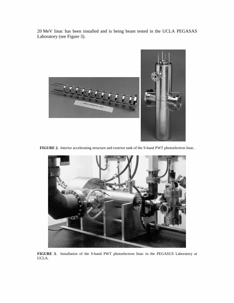
20 MeV linac has been installed and is being beam tested in the UCLA PEGASAS Laboratory (see Figure 3).
FIGURE 2. Interior accelerating structure and exterior tank of the S-band PWT photoelectron linac.
FIGURE 3. Installation of the S-band PWT photoelectron linac in the PEGASUS Laboratory at UCLA.
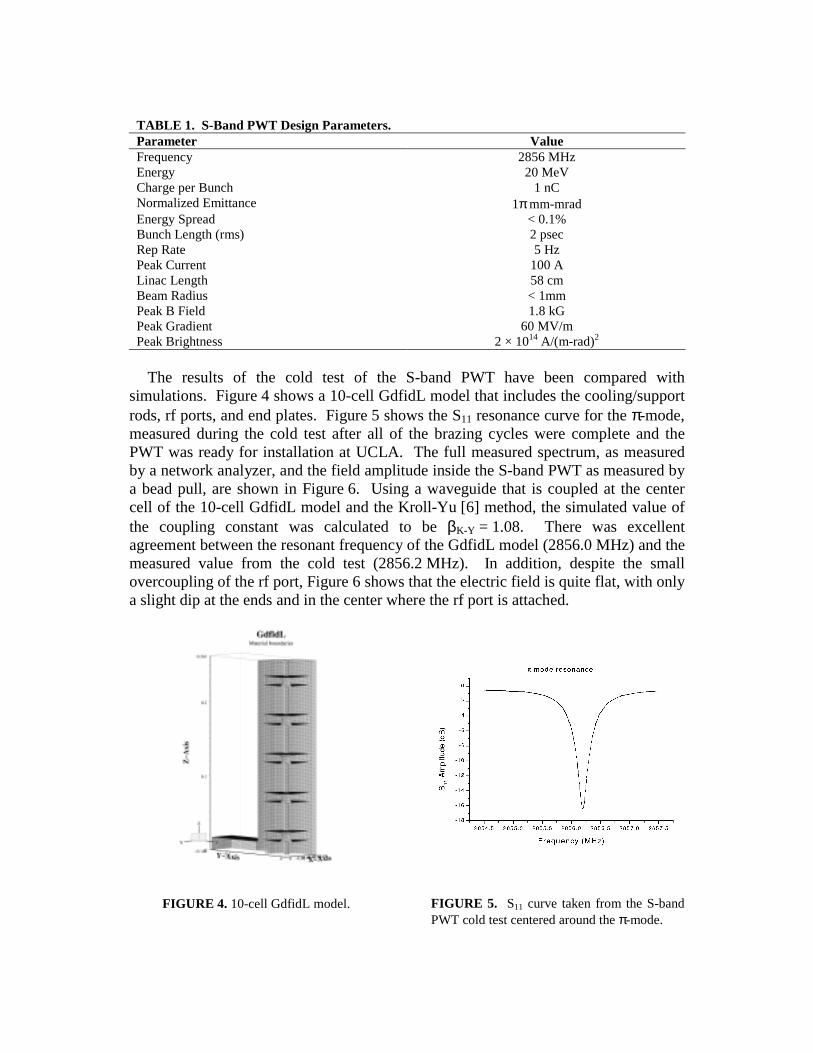
TABLE 1. S-Band PWT Design Parameters. Parameter Value Frequency 2856 MHz Energy 20 MeV Charge per Bunch 1 nC Normalized Emittance 1π mm-mrad Energy Spread < 0.1% Bunch Length (rms) 2 psec Rep Rate 5 Hz Peak Current 100 A Linac Length 58 cm Beam Radius < 1mm Peak B Field 1.8 kG Peak Gradient 60 MV/m Peak Brightness 2 × 10¹⁴ A/(m-rad)2
The results of the cold test of the S-band PWT have been compared with
simulations. Figure 4 shows a 10-cell GdfidL model that includes the cooling/support rods, rf ports, and end plates. Figure 5 shows the S11 resonance curve for the π-mode, measured during the cold test after all of the brazing cycles were complete and the PWT was ready for installation at UCLA. The full measured spectrum, as measured by a network analyzer, and the field amplitude inside the S-band PWT as measured by a bead pull, are shown in Figure 6. Using a waveguide that is coupled at the center cell of the 10-cell GdfidL model and the Kroll-Yu [6] method, the simulated value of the coupling constant was calculated to be βK-Y = 1.08. There was excellent agreement between the resonant frequency of the GdfidL model (2856.0 MHz) and the measured value from the cold test (2856.2 MHz). In addition, despite the small overcoupling of the rf port, Figure 6 shows that the electric field is quite flat, with only a slight dip at the ends and in the center where the rf port is attached.
FIGURE 4. 10-cell GdfidL model.
FIGURE 5. S11 curve taken from the S-band PWT cold test centered around the π-mode.

FIGURE 6. Full spectrum S11 curve and results of the bead pull measurement from the S-band PWT cold test.
There was an approximately 50% discrepancy between measured value of Qo
(12,450) and the value determined from GdfidL simulation (24,305). This difference between the observed value and the calculated value of Qo can have a significant effect on the efficiency of the linac. A 50% drop in Qo will result in a factor of 2 drop in the accelerating gradient.
Two possible mechanisms to explain this discrepancy were investigated. In the PWT design, the current that supports the magnetic field is carried on the surface of the cooling/support rods, as opposed to a disk-loaded design where the current is carried on the outer wall. The large number of braze joints in the S-band PWT results in an increased chance for an imperfect braze. Such a braze joint, with increased local resistivity, could impede the necessary flow of the current and result in greater losses in the rods. The greater loss in the rods results in a lower value of Qo. In order to try to model this possibility, a single-cell GdfidL model was used. To simulate the braze joint, a different value of the material resistivity was given to a small region between the cooling rod and the copper disk. Figure 7 shows the relative drop in the value of Qo as the resistivity of the braze material is increased. A 50% reduction in Qo, if attributed entirely to the braze defects, would require that the resistivity be increased by an overwhelming factor of 40,000. The braze material used in these joints was 40Au-60Cu which has a resistivity approximately 6 times larger than OFHC copper. The additional factor of ~7,000 required would have to be a result of inclusions, “bubbles”, or other imperfections in the braze material.
The tank walls and the cooling rods were constructed out of stainless steel, then copper plated prior to brazing. It is possible that some unknown contamination during the plating process and/or possible surface damage at the high brazing temperatures may cause the resistivity of these surfaces to be greater than was used in the GdfidL model. This is the second mechanism investigated to explain the decreased value of Qo. In the GdfidL model, the resistivity of the wall and rod material was increased from the original value corresponding to OFHC copper. The results are shown in Figure 8. To achieve the 50% reduction in Qo that is observed, the resistivity of the copper surfaces on the tank wall and rods must increase by a factor of 10. As a reference point, the resistivity of 304 stainless steel is approximately 40 times larger

than that of OFHC copper, and as mentioned before, the resistivity of the braze material is 7 times larger. If surface contamination or degradation is the source of the decreased value of Qo, then these issues should be reduced in the X-band PWT, where the smaller size allows for the cooling/support rods to be made from copper tubing instead of copper plated stainless steel.
0.2
0.3
0.4
0.5
0.6
0.7
0.8
0.9
1
1.E+00 1.E+01 1.E+02 1.E+03 1.E+04 1.E+05 1.E+06
Relative Resistivity of Braze Material (ρ/ρOFHC Copper)
Rel
ativ
e Q
o (Q
o /Q
o O
FHC
Cop
per)
FIGURE 7. Degradation of Qo as the relative resistivity of the braze material is increased.
0
0.1
0.2
0.3
0.4
0.5
0.6
0.7
0.8
0.9
1
0 2 4 6 8 10 12 14 16
Relative Wall & Rod Resistivity (ρ/ρ OFHC Copper)
Rel
ativ
e Q
o (Q
o/Q
o O
FHC
cop
per)
FIGURE 8. Degradation of Qo as the resistance of the walls and cooling rods is increased.
X-BAND PWT PHOTOELECTRON LINAC
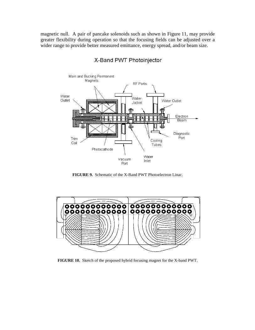
Spurred on by the success of the S-band PWT, DULY Research Inc. is now developing an X-band version of the integrated photoelectron linac. The X-band PWT photoelectron linac promises to produce an even brighter beam than the S-band PWT, due in part to the smaller bunch length and lower emittance of the beam. While in principle the physics of the PWT photoinjector linac is scaleable in frequency [7], the daunting engineering tasks of a high frequency integrated photoinjector linac are mandated by the requirements of a much higher magnetic field, higher accelerating gradient, and higher peak electric field – all in a smaller package. The development of this photoelectron linac is supported by an SBIR grant from the Department of Energy, and is conducted in collaboration with UCLA and ILSA/UCD at LLNL, where an X-band (8.547 GHz) klystron is available for beam tests.
A schematic of the X-band PWT is shown in Figure 9. A simple 1/3 scaling from the S-band PWT indicates that the required magnetic field should be on the order of 4-5.5 kG. This would require a solenoid magnet significantly larger than the one currently used on the S-band PWT and operating at much higher current. Such a magnet would dwarf the X-band structure and add potentially unnecessary bulk and expense to the final product. DULY has designed a hybrid magnet system, which is primarily comprised of permanent magnets, but uses solenoidal windings for precise trim. This hybrid-focusing magnet is shown in Figure 10 and has a footprint which is acceptable relative to the size of the linac. The primary disadvantage of a permanent magnet focusing system is the inability to make fine tune adjustment in the strength of the magnetic field. Currently, DULY is working on a hybrid magnet design in which the solenoidal windings play a more significant role than in the present design, shown in Figure 10, where the windings provide minor trim control of the position of the
magnetic null. A pair of pancake solenoids such as shown in Figure 11, may provide greater flexibility during operation so that the focusing fields can be adjusted over a wider range to provide better measured emittance, energy spread, and/or beam size.
FIGURE 9. Schematic of the X-Band PWT Photoelectron Linac.
FIGURE 10. Sketch of the proposed hybrid focusing magnet for the X-band PWT.
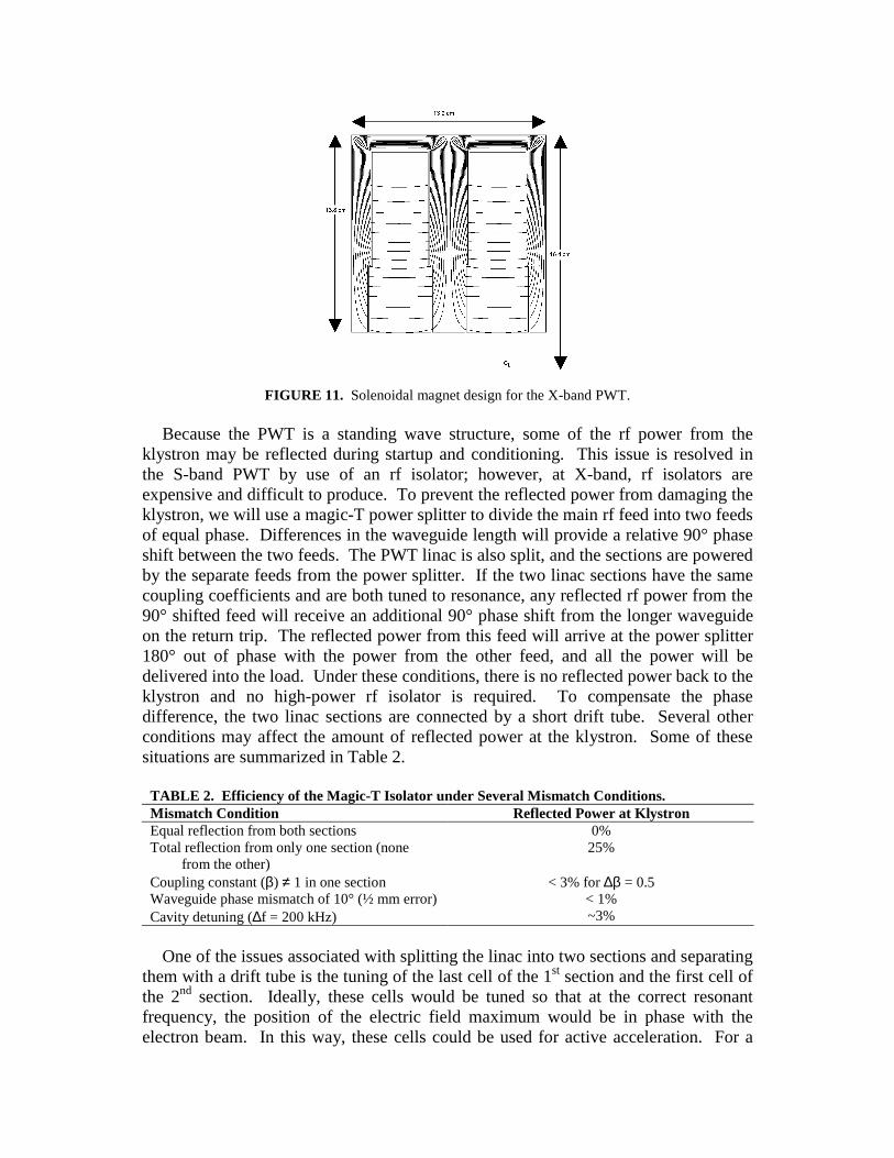
FIGURE 11. Solenoidal magnet design for the X-band PWT. Because the PWT is a standing wave structure, some of the rf power from the
klystron may be reflected during startup and conditioning. This issue is resolved in the S-band PWT by use of an rf isolator; however, at X-band, rf isolators are expensive and difficult to produce. To prevent the reflected power from damaging the klystron, we will use a magic-T power splitter to divide the main rf feed into two feeds of equal phase. Differences in the waveguide length will provide a relative 90° phase shift between the two feeds. The PWT linac is also split, and the sections are powered by the separate feeds from the power splitter. If the two linac sections have the same coupling coefficients and are both tuned to resonance, any reflected rf power from the 90° shifted feed will receive an additional 90° phase shift from the longer waveguide on the return trip. The reflected power from this feed will arrive at the power splitter 180° out of phase with the power from the other feed, and all the power will be delivered into the load. Under these conditions, there is no reflected power back to the klystron and no high-power rf isolator is required. To compensate the phase difference, the two linac sections are connected by a short drift tube. Several other conditions may affect the amount of reflected power at the klystron. Some of these situations are summarized in Table 2.
TABLE 2. Efficiency of the Magic-T Isolator under Several Mismatch Conditions. Mismatch Condition Reflected Power at Klystron Equal reflection from both sections 0% Total reflection from only one section (none
from the other) 25%
Coupling constant (β) ≠ 1 in one section < 3% for ∆β = 0.5 Waveguide phase mismatch of 10° (½ mm error) < 1% Cavity detuning (∆f = 200 kHz) ~3%
One of the issues associated with splitting the linac into two sections and separating
them with a drift tube is the tuning of the last cell of the 1st section and the first cell of the 2nd section. Ideally, these cells would be tuned so that at the correct resonant frequency, the position of the electric field maximum would be in phase with the electron beam. In this way, these cells could be used for active acceleration. For a

closed half-cell, like the first half-cell with the photocathode, the electric field maximum is at the metal wall. When an aperture is opened for the drift tube, the electric field is “pulled” into the drift tube and the electric field maximum shifts away from the wall. The main effect of this in the PWT structure is to add some spread in energy. Figure 12 shows a design of the 6+-cell X-band structure. The protrusion near the outer wall combined with the position of the end plate provides the ability to tune the frequency and the position of the peak electric field simultaneously.
When the drift tube transition cell is properly tuned, the electric field in the 6+-cell structure is flat, except for the transition cell. In this particular design, the transition cell has an electric field that is approximately 10% larger than the field in the main portion of the linac section (Figure 13). With other design choices, the field in the transition cell can be larger than, smaller than, or equal to the field in the other cells. When the tuning ring was shifted by 20 mil, SUPERFISH gave a frequency shift in the entire structure of δf/fo = 0.1% (9.2 MHz). The field flatness in the “normal” region was δE/E = 9%, and the electric field in the final cell was 2% lower than the average field in other (“normal”) cells. Because SUPERFISH is a 2D axisymmetric code, the cooling rods cannot be modeled; and these results are indicative of the order of magnitude of the effects. In a final detailed design of the X-band PWT integrated photoinjector, GdfidL will be used to perform a fully 3D simulation of the drift tube transition cell.
FIGURE 12. SUPERFISH model of the 6+-cell linac section for the X-band PWT.
FIGURE 13. Axial electric field plot for X-band PWT. From the results of the cold test measurement on the S-band PWT discussed above,
we should anticipate a reduction in the value of Qo for the X-band PWT as well. In

order to determine the effect this reduction in Qo has on the parameters of the X-band PWT, 4 cases are being studied using PARMELA. These cases are based on 19 MW output power from the klystron. Half of the cases use the ideal value of Qo as calculated by GdfidL, and the other half assume a value of ½Qo. Additionally, SLED pulse compression can provide additional power that is dependent upon Qo. The presence or absence of the SLED pulse compression combined with the ideal or reduced Qo give 4 different cases. The parameters for these cases are given in Table 3. SLED provides a 71% (144%) increase in rf power that translates into a 30% (11%) increase in the accelerating gradient for Case 2 (4) from the nominal X-band PWT design of Case 1. At this point, installation of a SLED pulse compression system is not a part of the project, but is intended as an upgrade after additional funding is secured. The result is that Case 3 should most closely reflect the initial operating regime of the X-band PWT.
TABLE 3. Four Operating Cases for X-Band PWT. Case Qo Power (MW) Eo (MV/m) SLED Comment 1 15,717 19.0 137.2 NO Ideal Qo 2 15,717 32.5 179.4 YES Ideal Qo 3 7,859 19.0 97.0 NO ½ Ideal Qo 4 7,859 46.4 151.6 YES ½ Ideal Qo
The normalized emittance curves for each of the 4 cases are shown in Figure 14, the
energy spreads are in Figure 15, the rms beam radii are in Figure 16, and a summary of the simulation results appears in Table 4. Currently, the input parameters are being studied to optimize each of these cases with a particular emphasis on Case 3. The parameter space for the input conditions is vast, and the search is a long process. As is clear from the data, Case 3 results in the worst beam parameters, making optimization critical. All of the PARMELA data presented in Table 3 used a charge per bunch of 1 nC. One option under strong consideration is to operate the X-band PWT at a total charge lower than the nominal 1 nC. When the system is upgraded with the SLED pulse compression, this limitation on the charge should not be necessary.
0
1
2
3
4
5
6
0 50 100 150 200Logitudinal Distance Z (cm)
Emitt
ance
(mm
-mra
d)
Case 1Case 2Case 3Case 4
FIGURE 14. Normalized rms emittance for the four operating cases in the X-band PWT obtained from PARMELA simulation.

0.0%
0.3%
0.6%
0.9%
1.2%
1.5%
1.8%
0 50 100 150 200Logitudinal Distance Z (cm)
Ener
gy S
prea
d, rm
s (%
)
Case 1Case 2Case 3Case 4
FIGURE 15. rms energy spread for the four operating cases in the X-band PWT obtained from PARMELA simulation.
0
0.2
0.4
0.6
0.8
1
1.2
1.4
0 50 100 150 200Logitudinal Distance Z (cm)
Beam
Rad
ius,
rms
(mm
)
Case 1Case 2Case 3Case 4
FIGURE 16. rms beam radius for the four operating cases in the X-band PWT obtained from PARMELA simulation.
TABLE 4. PARMELA Results for the Operating Cases (data at point of minimum emittance). Case Beam Energy
(MeV) Energy Spread
Emittance (mm-mrad)
Beam Radius (rms mm)
Brightness (1014 A/(m-rad)2)
1 23.30 0.37% 1.35 0.63 5.40 2 29.20 0.34% 1.11 < 0.70 11.9 3 16.59 1.38% 3.40 0.41 0.50 4 25.40 0.34% 1.24 1.1 7.40
ACKNOWLEDGMENTS
The authors would like to thank C. Pellegrini, P. Wilson, F. Hartemann, X. Ding, and S. Telfer for useful discussions, comments and technical assistance. This work is

supported by the U.S. Department of Energy SBIR Grants DE-FG03-96ER82159 and DE-FG03-98ER82566.
REFERENCES
1. D. Yu et al., Proc. of Particle Accelerator Conf., Vancouver, B.C. Canada, May 1997, p.2802. 2. D. Yu et al., Proc. of Particle Accelerator Conf., New York, NY, March 1999, p.2203. 3. D. Yu, Proc of 2nd ICFA Adv. Accel. Workshop, UCLA, November 1999, to be published. 4. V.B. Andreev, Soviet Physics — Technical Physics, 13, 1070 (1969). 5. D.A. Swenson., European Particle Accel. Conf., Rome, Italy, ed. S. Atzzari, 2 (1988). 6. N.M. Kroll and D. Yu, Particle Accelerators 34, 231-250 (1990). 7. J. Rosenzweig, N. Barov, and E. Colby, Proc. Adv. Accel. Concepts, p.724, AIP 335, 1995.

![PWT EN Dimensions - Klingenburg GmbH ... ENERG Y RECO VERY PWT EN 0216 Extremely robust and sealed Crossflow plate heat exchanger Type PWT PWT Dimensions Dimensions Type A [mm] B [mm]](https://static.fdocuments.in/doc/165x107/5aabb7d77f8b9ac55c8c3b6a/pwt-en-dimensions-klingenburg-gmbh-energ-y-reco-very-pwt-en-0216-extremely.jpg)