Rosemount Analytical 700XA Gas Chromatograph
12
A Digitally Assisted Telescopic Amplifier With Improved ICMR and Programmable Unity Gain Frequency RISHI TODANI National Institute of Technology Department of ECE Durgapur - 713209 INDIA [email protected] ASHIS KUMAR MAL National Institute of Technology Department of ECE Durgapur - 713209 INDIA [email protected] Abstract: Telescopic amplifiers are often preferred for their large DC gain, low power dissipation and low flicker noise. On the other side, they suffer from serious problems like poor input common mode range and output swing. In this work, a simple technique to improve the input common mode range of telescopic structure is presented. To achieve this, two telescopic amplifiers using complementary differential pairs are utilized. The proposed design incorporates a digital switching technique which enables to maintain a flat response throughout the extended input common mode range. It also provides a facility to elevate the performance of the circuit over a predefined range of input common mode level, at the cost of extra power. The entire design is verified using UMC 180 nm CMOS technology and the simulation results are presented. Key–Words: Analog design, CMOS; operational amplifier, telescopic amplifier, input common mode range, com- plementary amplifier. 1 Introduction Operational amplifiers are one of the most impor- tant building block of analog and mixed signal cir- cuits. Various topologies of amplifiers can be found in literature and research papers differentiated by their characteristic performance parameters. Amplifiers are primarily characterised by parameters like DC gain, output resistance, unity gain frequency (UGF), band- width, input common mode range (ICMR), output swing, power dissipation, etc. It is known that cascoding of transistors increases the output impedance and hence the gain of the am- plifier. Telescopic amplifiers are commonly used cas- coded architecture that features large DC gain from a single stage but suffers from serious problems like poor input common mode range (ICMR) and output swing [1]. ICMR issues are solved by folded cascode architecture where ICMR extends beyond the supply rail on at least one side [2]. Alternate schemes have also been proposed like the one given in [3] where the folded cascode opamp exhibits rail to rail ICMR by employing complementary input pair and sharing the load branch. However, folded cascode structures offer lesser gain, consume larger current due to presence of two branches and contribute more noise as compared to telescopic structures [4]. Several reports are found to increase the output swing of telescopic structures [5]. However, tech- niques to improve the ICMR of telescopic structure remains relatively unexplored. In this work, a simple scheme to extend the ICMR of telescopic structure us- ing complementary differential pair is presented. The scheme also includes a provision for enhancing the unity gain frequency of the amplifier over a range of input common mode level. 2 Typical Telescopic Amplifiers A typical NMOS differential pair based fully differen- tial telescopic amplifier with common mode feedback (CMFB) circuit is shown in Figure 1. Transistors Mn1 to Mn9 form the telescopic amplifier while Mn10 to Mn17 form the common mode feedback (CMFB) cir- cuit. Mathematically, the ICMR (ICMR − to ICMR + ) of this amplifier can be expressed as ICMR + NMOS = V out - V DS,sat(Mn4) - V DS,sat(Mn2) + V GS(Mn2) (1) ICMR − NMOS = V DS,sat(Mn9) + V GS(Mn2) (2) Similarly, PMOS differential pair based fully differen- tial telescopic amplifier with CMFB circuit is shown in Figure 2 with transistors Mp1 though Mp9 forming WSEAS TRANSACTIONS on CIRCUITS and SYSTEMS Rishi Todani, Ashis Kumar Mal E-ISSN: 2224-266X 301 Volume 13, 2014
Transcript of Rosemount Analytical 700XA Gas Chromatograph

A Digitally Assisted Telescopic Amplifier With Improved ICMR
and Programmable Unity Gain Frequency
RISHI TODANI
National Institute of Technology
Department of ECE
Durgapur - 713209
INDIA
ASHIS KUMAR MAL
National Institute of Technology
Department of ECE
Durgapur - 713209
INDIA
Abstract: Telescopic amplifiers are often preferred for their large DC gain, low power dissipation and low flicker
noise. On the other side, they suffer from serious problems like poor input common mode range and output swing.
In this work, a simple technique to improve the input common mode range of telescopic structure is presented. To
achieve this, two telescopic amplifiers using complementary differential pairs are utilized. The proposed design
incorporates a digital switching technique which enables to maintain a flat response throughout the extended input
common mode range. It also provides a facility to elevate the performance of the circuit over a predefined range
of input common mode level, at the cost of extra power. The entire design is verified using UMC 180 nm CMOS
technology and the simulation results are presented.
Key–Words: Analog design, CMOS; operational amplifier, telescopic amplifier, input common mode range, com-
plementary amplifier.
1 Introduction
Operational amplifiers are one of the most impor-
tant building block of analog and mixed signal cir-
cuits. Various topologies of amplifiers can be found
in literature and research papers differentiated by their
characteristic performance parameters. Amplifiers are
primarily characterised by parameters like DC gain,
output resistance, unity gain frequency (UGF), band-
width, input common mode range (ICMR), output
swing, power dissipation, etc.
It is known that cascoding of transistors increases
the output impedance and hence the gain of the am-
plifier. Telescopic amplifiers are commonly used cas-
coded architecture that features large DC gain from
a single stage but suffers from serious problems like
poor input common mode range (ICMR) and output
swing [1]. ICMR issues are solved by folded cascode
architecture where ICMR extends beyond the supply
rail on at least one side [2]. Alternate schemes have
also been proposed like the one given in [3] where the
folded cascode opamp exhibits rail to rail ICMR by
employing complementary input pair and sharing the
load branch. However, folded cascode structures offer
lesser gain, consume larger current due to presence of
two branches and contribute more noise as compared
to telescopic structures [4].
Several reports are found to increase the output
swing of telescopic structures [5]. However, tech-
niques to improve the ICMR of telescopic structure
remains relatively unexplored. In this work, a simple
scheme to extend the ICMR of telescopic structure us-
ing complementary differential pair is presented. The
scheme also includes a provision for enhancing the
unity gain frequency of the amplifier over a range of
input common mode level.
2 Typical Telescopic Amplifiers
A typical NMOS differential pair based fully differen-
tial telescopic amplifier with common mode feedback
(CMFB) circuit is shown in Figure 1. Transistors Mn1
to Mn9 form the telescopic amplifier while Mn10 to
Mn17 form the common mode feedback (CMFB) cir-
cuit. Mathematically, the ICMR (ICMR− to ICMR+)
of this amplifier can be expressed as
ICMR+NMOS = V out− VDS,sat(Mn4)
− VDS,sat(Mn2) + VGS(Mn2)
(1)
ICMR−
NMOS = VDS,sat(Mn9) + VGS(Mn2) (2)
Similarly, PMOS differential pair based fully differen-
tial telescopic amplifier with CMFB circuit is shown
in Figure 2 with transistors Mp1 though Mp9 forming
WSEAS TRANSACTIONS on CIRCUITS and SYSTEMS Rishi Todani, Ashis Kumar Mal
E-ISSN: 2224-266X 301 Volume 13, 2014

Vdd
Mn1 Mn2
Mn3 Mn4
Mn5 Mn6
Mn7Mn8
Mn9
CloadCload
Vbias1
Vbias2
Vbias3
Vin-
Vout+Vout-
Vin+
Vout-
Vdd
Mn10Mn11
Mn12 Mn13 Mn14 Mn15
Mn16 Mn17
Vcm
D
VCMFB
A B
X Y
Figure 1: Typical Telescopic Amplfiers with CMFB
and NMOS Input Pair
the telescopic amplifier and Mp10 to Mp17 forming
the CMFB circuit. The ICMR of this structure can be
given by
ICMR+PMOS = VDD − |VDS,sat(Mp9)|
− |VGS(Mp2)|(3)
ICMR−
PMOS = V out+ |VDS,sat(Mp4)|+ |VDS,sat(Mp2)| − |VGS(Mp2)|
(4)
For a 1.8 V technology, the typical response of
amplifiers shown in Fig. 1 and 2 is listed in Table 1.
The parameters are measured keeping input and out-
put common mode level at VDD/2 = 0.9 V. The two
amplifiers are designed using Potential Distribution
Method (PDM) [6, 7, 8]. The NMOS input pair based
amplifier consumes 20 µA at each tail transistor Mn9,
Vdd
Mp1 Mp2
Mp3 Mp4
Mp5 Mp6
Mp7 Mp8
Mp9
CloadCload
Vbias1
Vbias2
Vbias3
Vin-
Vout+Vout-
Vin+
Vout-
Vdd
Mp16 Mp17
Mp12 Mp13 Mp14 Mp15
Mp10 Mp11
Vcm
VCMFB
A B
X Y
Figure 2: Typical Telescopic Amplfiers with CMFB
and PMOS Input Pair
Mn16 and Mn17. For matching the performance of
the PMOS based amplifier with that of NMOS based,
the source currents of PMOS based amplifier is set
to 24 µA at transistors Mp9, Mp16 and Mp17, and its
node potentials are adjusted as suggested by PDM [7].
It may be mentioned that designing a PMOS based
amplifier matching the AC response of NMOS based
amplifier was easily achieved by applying PDM. For
achieving large ICMR and for comparative purpose,
the overdrive of all transistors in both amplifiers are
kept at about 5% of VDD. It is known that both
the amplifiers see a dominant pole at the output node
and a non-dominant pole at node A (or B) [4]. The
dominant pole of the two amplifiers are nearly at the
same location. However, the non-dominant pole of
the PMOS input pair based amplifier is much lower
than its NMOS counterpart. This is due to the fact
that in PMOS based amplifier, the capacitance at node
A (or B) is accounted by PMOS transistors while in
NMOS based amplifier, by NMOS transistors. For
carrying the same current, at identical overdrive and
channel length, PMOS transistors are around 3 to 4
times wider than NMOS transistors and hence capac-
itance at node A (or B) of PMOS based amplifier is
much larger than that of NMOS based amplifier.
Table 1 clearly shows that the AC response pa-
rameters like DC gain, −3 dB bandwidth, unity
gain frequency (UGF), transconductance and domi-
nant pole of the two amplifiers closely match. From
this table it is evident that telescopic architectures ex-
hibit small ICMR but large DC gain even with a single
stage. It is to be noted that NMOS based amplifier has
lower ICMR− than PMOS based, while PMOS based
amplifier has larger ICMR+ than NMOS based. The
input common mode response of the amplifiers is now
studied.
The AC response of the amplifiers over a wide
range of input common mode level are shown in Fig-
ure 3 and 4. It is clear that the response of the two am-
plifiers are comparable over the range of input com-
mon mode level. The phase margin of both ampli-
fiers remain around 85◦ to 90◦ throughout the range
of input common mode. From Figure 3 and 4 it may
be concluded that the ICMR of telescopic structure
can be improved if we operate NMOS differential pair
based amplifier when input common mode level is
below VDD/2 or 0.9 V and PMOS differential pair
based amplifier when input common mode level is
above VDD/2 or 0.9 V. However, there is a region
around 0.9 V where both amplifiers work satisfacto-
rily (from ICMR−
PMOS to ICMR+NMOS). In this re-
gion, both, NMOS and PMOS based amplifiers can be
made to work in parallel and we can achieve elevated
or improved performance.
WSEAS TRANSACTIONS on CIRCUITS and SYSTEMS Rishi Todani, Ashis Kumar Mal
E-ISSN: 2224-266X 302 Volume 13, 2014

Table 1: Response of Typical Telescopic Amplifiers
Performance NMOS Differential Pair PMOS Differential Pair
Parameter Based Amplifier Based Amplifier
@ Vin,dc = 0.9 V (Figure 1) (Figure 2)
ICMR− 0.62 V 0.85 V
ICMR+ 0.95 V 1.06 V
ICMR 0.33 V 0.21 V
% ICMR 18% 11%
CLoad 1 pF 1 pF
DC Gain 62.42 dB 62.41 dB
UGF 21.12 MHz 20.37 MHz
-3 dB Bandwidth 15.67 kHz 15.81 kHz
Phase Margin 89.4◦ 87.6◦
Transconductance (gm) 140 µA/V2 135 µA/V2
Tail Current (ITail) 20 µA 24 µA
CMFB Current (ICMFB) 20 µA 24 µA
Total Current 60 µA 72 µA
Power Dissipation 108 µW 129.6 µW
Slew Rate 20 V/µs 24 V/µs
Dominant Pole 15.98 kHz 15.45 kHz
Non-Dominant Pole 2.09 GHz 519.3 MHz
CMRR 270.5 dB 312.4 dB
PSRR 237.5 dB 242.2 dB
Total Input Referred Noise115.76 µV/
√Hz 151.21 µV/
√Hz
(1 Hz to 20 MHz)
3 Proposed Telescopic Amplifier
The block diagram of the proposed telescopic ampli-
fier structure is shown in Figure 5. It comprises of
mainly four parts, the two complementary telescopic
amplifiers in parallel, based on NMOS and PMOS in-
put pairs, an amplifier selection and power control cir-
cuit and an output selection circuit. Two reference
voltages and a low power enable signals are applied
externally such that, when the input common mode
level is below lower reference voltage, only NMOS
input pair based amplifier remains active and when
input common mode level is above upper reference,
only PMOS input pair based amplifier remains active.
When input common mode level is between the two
references, both the amplifiers are activated and oper-
ate in parallel. The amplifier selection and power con-
trol circuit is responsible for generating control sig-
nals for activating and deactivating the amplifiers or
switching to low power mode when both amplifiers
are on. The output selection circuit connects the out-
puts of the amplifier to the load as per the input com-
mon mode level.
3.1 Amplifier Selection And Power Control
Circuit
The amplifier selection and power control circuit is re-
sponsible for generating digital signals to on/off the
amplifiers and control power dissipation when both
amplifiers are on.
The inputs to this circuit are the two reference
values (Vref+ and Vref−), along with either of the
inputs (Vin+ or Vin−). Let the DC level of the in-
WSEAS TRANSACTIONS on CIRCUITS and SYSTEMS Rishi Todani, Ashis Kumar Mal
E-ISSN: 2224-266X 303 Volume 13, 2014

0.5 0.6 0.7 0.8 0.9 1 1.1 1.2 1.3−10
0
10
20
30
40
50
60
70
Input Common Mode Level (V)
DC
Ga
in (
dB
)
PMOSNMOS
(a)
0.5 0.6 0.7 0.8 0.9 1 1.1 1.2 1.360
70
80
90
100
110
120
130
140
150
Input Common Mode Level (V)
Tra
nsc
on
du
cta
nce
(µ
A/V
2)
NMOS
PMOS
(b)
Figure 3: Response Of Typical Telescopic Amplfiers (a) DC Gain (b) Transconductance (gm)
0.5 0.6 0.7 0.8 0.9 1 1.1 1.2 1.32
4
6
8
10
12
14
16
18
20
22
24
Input Common Mode Level (V)
Un
ity G
ain
Fre
qu
ency
(U
GF
) (M
Hz)
PMOSNMOS
(a)
0.5 0.6 0.7 0.8 0.9 1 1.1 1.20
10
20
30
40
50
60
70
80
90
100
Input Common Mode Level (V)
−3 d
B B
an
dw
idth
(K
Hz)
NMOS PMOS
(b)
Figure 4: Response Of Typical Telescopic Amplifiers (a) Unity Gain Frequency (UGF) (b) −3 dB Bandwidth
put be denoted by Vin,dc. The reference voltages are
now chosen which marks the switching point of the
amplifiers. It also defines the range over which both
the amplifiers operate (when input common mode is
between the two references). Typically, they are cho-
sen above and below VDD/2. Since during this range,
both amplifiers operate, Vref− can have a minimum
value equal ICMR−
PMOS and Vref+ can have a max-
imum value equal ICMR+NMOS.
Depending upon the the DC level of the input
voltage Vin,dc, control signals n select and p select
are generated. As long as Vin,dc < Vref+, n select
= VDD (logic high), and as long as Vin,dc > Vref−,
p select = VDD (logic high). When the Vin,dc is be-
tween the two references, n select = p select = VDD.
The signals n select and p select are used to turn on
the NMOS and PMOS based amplifiers respectively.
This block generates another signal labelled
ctrl which goes high when n select, p select and
low power en are high at the same time. The sig-
nal low power en is used to activate low power mode
when both amplifiers are on. The low power mode
makes both the amplifier circuits consume half cur-
rent, keeping total current more or less flat throughout
ICMR. The signals n select and p select can be gener-
ated by comparing the input common mode with ref-
erence voltages using comparators [9]. The signal ctrl
is simply the logical AND of n select, p select and
low power en.
Table 2 shows the logical values of signals pro-
duced by the amplifier selection and power control
circuit under the three cases of input DC level, with
low power mode enabled and disabled. It can be seen
WSEAS TRANSACTIONS on CIRCUITS and SYSTEMS Rishi Todani, Ashis Kumar Mal
E-ISSN: 2224-266X 304 Volume 13, 2014

Telescopic Opamp
Fully Differential
with NMOS
differential pair
Telescopic Opamp
Fully Differential
with PMOS
differential pair
Power Control
Circuit
Amplifier Selection
&
Circuit
Output n_selectctrl
p_select
Voutn+
Voutn-
Voutp-
Voutp+
L
O
A
D
Vout+
Vout-
Vin+
Vin-
Modified
Modified
Selection
Vref+
Vref-
low_power_en
Figure 5: Block Diagram Of Proposed Telescopic Amplifier
Table 2: Amplifier Selection and Power Control Circuit Outputs (H: Logic High (1.8 V); L: Logic Low (0 V))
Case Input Common Mode (Vin,dc) n select p select low power en ctrl
I Vin,dc < Vref− H LH H
L H
II Vref− < Vin,dc < Vref+ H HH L
L H
III Vin,dc > Vref+ L HH H
L H
from the table that when both amplifiers are on, as in
Case II, and low power mode is enabled (logic high),
ctrl becomes low. These are used to open the switches
in amplifier circuits to cut out half the current and
reduce power dissipation. At other times, ctrl stays
high, switches remain closed and the amplifier circuit
draws full current.
3.2 Output Selection Circuit
The output selection circuit can be designed as a sim-
ple arrangement of switches implemented using trans-
mission gates which connect the outputs of the two
amplifiers across the load. The transmission gates are
driven by same signal which activates/deactivates the
amplifiers (n select and p select). Whichever ampli-
fier is on, the transmission gate in its path is turned
on and amplifier output node is connected across the
load. When an amplifier turns off, its output node is
disconnected from across the load.
3.3 NMOS Differential Pair Based Amplifier
The NMOS differential pair based telescopic amplifier
shown in Figure 6(a) has three modes of operation.
First, full current mode where tail current is 20 µA.
Second, half current mode where all currents reduce
to half of full current. Third, turn off mode where all
currents become zero.
In deep sub-micron devices, for reducing currents
to half, simply reducing the transistor widths by half
while keeping overdrive and channel length constant
does not work. To arrive to the transistors widths for
Figure 6(a), two amplifiers like shown in Figure 1 are
WSEAS TRANSACTIONS on CIRCUITS and SYSTEMS Rishi Todani, Ashis Kumar Mal
E-ISSN: 2224-266X 305 Volume 13, 2014

Vdd
Mn1a Mn2a
Mn3a Mn4a
Mn5a Mn6a
Mn7a Mn8a
Mn9a
Vbias1
Vbias2
Vbias3
Vin-Vin+
Vbias1
Vbias2
Vbias3
Mn1b
Mn9b
Mn2b
Mn8b
Mn6b
Mn4b
Mn7b
Mn3b
Mn5b
Voutn
-
Voutn
+
VCMFB
n_select
ctrl
ctrl
ctrl
MnOFF1
ITail
A B
X Y
ctrl
ctrl
(a)
Vdd
Mp1a Mp2a
Mp3a Mp4a
Mp5a Mn6a
Mp7a Mp8a
Mp9a
Vbias1
Vbias2
Vbias3
Vin-Vin+
Vbias1
Vbias2
Vbias3
Mp1b
Mp9b
Mp2b
Mp8b
Mp6b
Mp4b
Mp7b
Mp3b
Mp5b
Voutp
-
Voutp
+
VCMFB
p_select
ctrl
ctrl
ctrl
ctrl
ctrl
MpOFF1
ITail
A B
X Y
(b)
Figure 6: (a) Modified NMOS Based Telescopic Amplifier (b) Modified PMOS Based Telescopic Amplifier
designed, one with full current (20 µA tail current),
and one with half current (10 µA tail current). Let the
transistor widths be denoted by W20 and W10 respec-
tively. The two amplifiers must have the same node
potential (drain to source drops and gate overdrive) so
that ICMR is maintained. The length of all transistors
are kept constant and identical for simplicity.
For the amplifier shown in Figure 6(a), all tran-
sistors labelled MnXa, where X takes value from 1 to
9, have widths equal to the corresponding transistor
in amplifier carrying half tail current (W10). While all
transistors labelled MnXb have widths equal to the dif-
ference between the widths of transistors carrying full
current and half current (W20-W10). As already men-
tioned, this way of sizing is necessary in deep sub-
micron devices. The CMFB circuit is not shown but
is designed in same way as the amplifying branch.
During Case I of Table 2, ctrl is always high. As
a result, all switches are closed and effective channel
width of all transistors is equal to W20. The ampli-
fier circuit thus draws full current. During Case II,
as long as low power mode is disabled, circuit still
draws full current. When ctrl goes low to activate
power saving mode, switches open thereby cutting out
all transistors labelled MnXb. The effective channel
width now becomes equal to W10 since only transis-
tors labelled MnXa conduct. The current consumption
thus becomes half. An additional transistors labelled
MnOFF1 is used to turn off this amplifier. It is driven
by the n select signal generated by the amplifier se-
lection and power control circuit. Finally, during Case
III, this amplifier turns off. The switches can be im-
plemented using transmission gates.
Just like the traditional telescopic amplifier, the
dominant pole of this amplifier is located at the output
node and the non-dominant pole at node A (or B). The
WSEAS TRANSACTIONS on CIRCUITS and SYSTEMS Rishi Todani, Ashis Kumar Mal
E-ISSN: 2224-266X 306 Volume 13, 2014

two poles are given by equations (5) and (6).
Dom. Pole ⇒ ωp,V outn =1
RV outn × CV outn
(5)
Non-Dom. Pole ⇒ ωp,B(NMOS) =gm4
CB(NMOS)(6)
where,
RV outn ≈ (gm4 ro4 ro2) || (gm6 ro6 ro8) (7)
CV outn ≈ Cdb4 + Cdg4 + Cdb6 + Cdg6 (8)
CB(NMOS) ≈ Cdb2 + Cdg2 +Csb4 + Cgs4 (9)
The ICMR of the amplifier shown in Figure 6(a)
is same as that of the amplifier shown in Figure 1 since
all overdrives and channel lengths are kept constant.
As already mentioned, the ICMR− of the proposed
structure is decided by NMOS input pair based ampli-
fier. It is expressed as,
ICMR− = VDS,sat(Mn9a) + VGS(Mn2a) (13)
3.4 PMOS Differential Pair Based Amplifier
The PMOS differential pair based telescopic ampli-
fier is shown in Figure 6(b). The design procedure and
transistor sizing is done in the same way as the NMOS
based amplifier. This amplifier consumes a current of
24 µA at tail transistor in full current mode. During
half current mode, ctrl goes low, all switches open and
thus current through all transistors labelled MpXb be-
come zero and overall current reduces to half. Transis-
tor labelled MpOFF1 is responsible for turning off/on
the amplifier. It is driven by p select which turns low
in Case I of Table 2. During Cases II and III, PMOS
based amplifier remains on. The dominant and non-
dominant pole of this amplifier are also due to output
node and node A (or B) respectively and is given by
equations (14) and (15).
Dom. Pole ⇒ ωp,V outp =1
RV outp × CV outp
(14)
Non-Dom. Pole ⇒ ωp,B(PMOS) =gm4
CB(PMOS)(15)
where,
RV outp ≈ (gm4 ro4 ro2) || (gm6 ro6 ro8) (16)
CV outp ≈ Cdb4 + Cdg4 + Cdb6 + Cdg6 (17)
CB(PMOS) ≈ Cdb2 + Cdg2 + Csb4 + Cgs4 (18)
The right hand side of equations (15) to (18) have
analogous interpretations as discussed earlier in equa-
tions (10) to (12). The ICMR+ of the proposed struc-
ture is decided by PMOS input pair based amplifier. It
is expressed as,
ICMR+ = VDD−|VDS,sat(Mp9a)|− |VGS(Mp2a)|(19)
The dominant pole of the complete structure is given
by
Dominant Pole ⇒ ωp,out =1
Rout × Cout
(20)
where,
Rout = RV outn || RV outp (21)
Cout = Cload + CV outn + CV outp (22)
As discussed earlier, the non-dominant pole arises
due to node B of both the amplifier circuits. However,
since node B of PMOS based amplifier see a larger ca-
pacitance than node B of NMOS based amplifier, the
non-dominant pole of entire circuit is due to node B of
PMOS based amplifier and is given by equation (18).
The voltage gain of the proposed structure can be
expressed as
Av = gm ×Rout (23)
where, The expression for Rout is also derived as per
the region of operation and using equations (7), (10),
(11), (16) and (21).
During Case II of Table 2, when low power mode
is disabled, both amplifiers are on and conduct full
current. At this time, the transconductance is double
as compared to the other times. This is due to dou-
bling of drain currents. However, due to almost dou-
bled transistor width, the output resistance is halved
and the overall DC gain remains the same. At other
times, the transconductance and output resistance re-
main almost constant for the entire ICMR maintaining
the DC gain.
4 Simulation
In this section, simulations methods and results are
discussed.
4.1 Simulation Methods
The complete design was implemented using UMC
180 nm CMOS technology in Cadence environment.
The circuit was first put into low power mode and
WSEAS TRANSACTIONS on CIRCUITS and SYSTEMS Rishi Todani, Ashis Kumar Mal
E-ISSN: 2224-266X 307 Volume 13, 2014

gmi =
{
gm(Mnia) + gm(Mnib) if low power disabled
gm(Mnia) if low power enabled
}
for i = 4, 6 (10)
roj =
{
ro(Mnja) || ro(Mnjb) if low power disabled
ro(Mnja) if low power enabled
}
for j = 2, 4, 6, 8 (11)
CXk =
{
CX(Mnka) + CX(Mnkb) if low power disabled
CX(Mnka) if low power enabled
}
for X = db, dg, sb, gs; k = 2, 4, 6 (12)
gm =
gm(Mn2a) + gm(Mn2b) Case I
gm(Mn2a) + gm(Mn2b) + gm(Mp2a) + gm(Mp2b) Case II; low power disabled
gm(Mn2a) + gm(Mp2a) Case II; low power enabled
gm(Mp2a) + gm(Mp2b) Case III
(24)
thorough response was observed. Then low power
mode was disabled and the observations are redone.
The graphs obtained during the two modes of opera-
tion were compared and are presented ahead.
4.2 Simulation Results
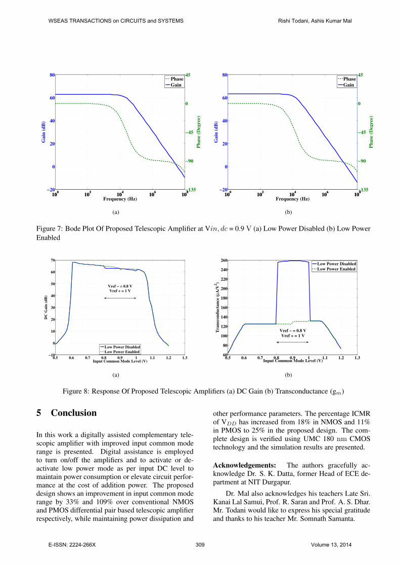
The simulation results are presented from Figure 7 to
11 and Table 3. Figure 7(a) and 7(b) show the bode
plots for the proposed amplifier circuit with low power
mode disabled and enabled respectively, with input
and output common mode at VDD/2 = 0.9 V and load
capacitance of 1 pF. When low power mode is dis-
abled, both amplifiers consume full current. When
enabled, they consume half the current. From Fig-
ure 7 it is clear that the circuit sees only one pole, the
dominant pole, before the unity gain frequency.
The complete response of the proposed circuit is
given in Table 3. Since the non-dominant pole ap-
pears much beyond the unity gain frequency, the cir-
cuit is stable. The DC gain in the two modes of op-
eration is fairly the same. The response of the pro-
posed amplifier in low power mode is almost match-
ing the response of the typical amplifiers from Ta-
ble 1. When low power mode is disabled, both the
amplifier circuits consume full current leading to in-
creased current but twice the bandwidth, transcon-
ductance and slew rate. The UGF increases by 1.5
times due to simultaneous increase in capacitance at
output node because of increased effective transistor
width, along with doubling of transconductance (UGF
= gm/Cout) [10]. The ICMR in both the modes re-
mains the same since all node voltages are maintained.
Small reduction in input referred noise is also seen
when full current is drawn.
To illustrate the response of the proposed struc-
ture over the range of ICMR, Figure 8 to 10 are
plotted. The reference voltages for amplifier selec-
tion are kept at 0.8 V and 1 V for all the graphs.
Figure 8(a) shows that the DC gain of the amplifier
remains more or less constant, with or without low
power mode enabled. From Figure 8(b) it can seen
that the transconductance remains constant through-
out the range of ICMR with low power mode enabled.
When low power mode is disabled, the transconduc-
tance doubles in the range between the two reference
voltages. This is due to doubling of drain currents at
constant overdrive. In this region, performance eleva-
tion is achieved at the expense of increased power dis-
sipation. Consequential effects in the UGF and band-
width are also seen due to doubling of transconduc-
tance and reduction in output resistance. The phase
margin, depicted in Figure 10(a), however remains
constant throughout the ICMR. Figure 10(b) shows
an estimated current consumption over the range of
ICMR.
To show the transient behaviour, the proposed
amplifier is connected in unity feedback mode and a
step input lying within its ICMR is applied. The re-
sponse is shown in Figure 11. The signal swing is
chosen such that the circuit passes through all three
regions of operation. The transistor widths of the final
design in given in Table 4. The other transistors which
are operating with digital inputs can be designed with
minimum size or any other size as suitable for the de-
signer such that the drop across them in negligible
when on.
WSEAS TRANSACTIONS on CIRCUITS and SYSTEMS Rishi Todani, Ashis Kumar Mal
E-ISSN: 2224-266X 308 Volume 13, 2014
100
102
104
106
108
−20
0
20
40
60
80
Gain
(d
B)
Frequency (Hz)10
010
210
410
610
8−135
−90
−45
0
45
Ph
ase
(D
egre
e)
Phase
Gain
(a)
100
102
104
106
108
−20
0
20
40
60
80
Gain
(d
B)
Frequency (Hz)10
010
210
410
610
8−135
−90
−45
0
45
Ph
ase
(D
egre
e)
Phase
Gain
(b)
Figure 7: Bode Plot Of Proposed Telescopic Amplifier at Vin, dc = 0.9 V (a) Low Power Disabled (b) Low Power
Enabled
0.5 0.6 0.7 0.8 0.9 1 1.1 1.2 1.3−10
0
10
20
30
40
50
60
70
Input Common Mode Level (V)
DC
Gain
(d
B)
Low Power Disabled
Low Power Enabled
Vref − = 0.8 V
Vref + = 1 V
(a)
0.5 0.6 0.7 0.8 0.9 1 1.1 1.2 1.360
80
100
120
140
160
180
200
220
240
260
Input Common Mode Level (V)
Tra
nsc
on
du
ctan
ce (
µA
/V2)
Low Power Disabled
Low Power Enabled
Vref − = 0.8 V
Vref + = 1 V
(b)
Figure 8: Response Of Proposed Telescopic Amplifiers (a) DC Gain (b) Transconductance (gm)
5 Conclusion
In this work a digitally assisted complementary tele-
scopic amplifier with improved input common mode
range is presented. Digital assistance is employed
to turn on/off the amplifiers and to activate or de-
activate low power mode as per input DC level to
maintain power consumption or elevate circuit perfor-
mance at the cost of addition power. The proposed
design shows an improvement in input common mode
range by 33% and 109% over conventional NMOS
and PMOS differential pair based telescopic amplifier
respectively, while maintaining power dissipation and
other performance parameters. The percentage ICMR
of VDD has increased from 18% in NMOS and 11%
in PMOS to 25% in the proposed design. The com-
plete design is verified using UMC 180 nm CMOS
technology and the simulation results are presented.
Acknowledgements: The authors gracefully ac-
knowledge Dr. S. K. Datta, former Head of ECE de-
partment at NIT Durgapur.
Dr. Mal also acknowledges his teachers Late Sri.
Kanai Lal Samui, Prof. R. Saran and Prof. A. S. Dhar.
Mr. Todani would like to express his special gratitude
and thanks to his teacher Mr. Somnath Samanta.
WSEAS TRANSACTIONS on CIRCUITS and SYSTEMS Rishi Todani, Ashis Kumar Mal
E-ISSN: 2224-266X 309 Volume 13, 2014

Table 3: Response of Proposed Telescopic Structure
Performance Parameters Proposed Structure (Fig. 5) Typical NMOS Typical PMOS
@ Vin,dc = 0.9 V Low Power Low Power Based Based
Disabled Enabled (Figure 1) (Figure 2)
ICMR− 0.62 V 0.62 V 0.62 V 0.85 V
ICMR+ 1.06 V 1.06 V 0.95 V 1.06 V
ICMR 0.44 V 0.44 V 0.33 V 0.21 V
% ICMR of VDD 25% 25% 18% 11%
% Increase in ICMR33%, 109% 33%, 109% - -
Over Fig. 1, Fig. 2
CLoad 1 pF 1 pF 1 pF 1 pF
DC Gain 62.72 dB 63.19 dB 62.42 dB 62.41
UGF 33.46 MHz 20.85 MHz 21.12 MHz 20.37 MHz
−3 dB Bandwidth 24.36 kHz 13.91 kHz 15.67 kHz 15.81 kHz
Phase Margin 83.2◦ 86.38◦ 89.4◦ 87.6◦
Transconductance (gm) 258.6 µA/V2 149.7 µA/V2 140 µA/V2 135 µA/V2
Total Current 132 µA 66 µA 60 µA 72 µA
Power Dissipation 237.6 µW 118.8 µW 108 µW 129.6 µW
Slew Rate 44 V/µs 22 V/µs 20 V/µs 24 V/µs
Dominant Pole 24.54 kHz 14.2 kHz 15.98 kHz 15.45 kHz
Non-Dominant Pole 371.8 MHz 381.7 MHz 2.09 GHz 519.3 MHz
CMRR 226 dB 223.42 dB 270.5 dB 312.4 dB
PSRR 214.12 dB 211.23 dB 237.5 dB 242.2 dB
Total Input Referred Noise101.05 µV/
√Hz 115.62 µV/
√Hz 115.76 µV/
√Hz 151.21 µV/
√Hz
(1 Hz to 20 MHz)
252 253 254 255 256 257−200
−100
0
100
200
Time (µsec)
Dif
fere
nti
al
Volt
age
(mV
)
Input
Output
Figure 11: Step Response of Proposed Telescopic
Amplifier
WSEAS TRANSACTIONS on CIRCUITS and SYSTEMS Rishi Todani, Ashis Kumar Mal
E-ISSN: 2224-266X 310 Volume 13, 2014

0.5 0.6 0.7 0.8 0.9 1 1.1 1.2 1.30
5
10
15
20
25
30
35
Input Common Mode Level (V)
Un
ity
Ga
in F
req
uen
cy (
UG
F)
(MH
z)
Low Power Disabled
Low Power Enabled
Vref − = 0.8 V
Vref + = 1 V
(a)
0.6 0.7 0.8 0.9 1 1.10
10
20
30
40
50
60
70
80
90
100
Input Common Mode Level (V)
−3
dB
Ba
nd
wid
th (
KH
z)
Low Power Disabled
Low Power Enabled
Vref − = 0.8 V
Vref + = 1 V
(b)
Figure 9: Response Of Proposed Telescopic Amplifiers (a) Unity Gain Frequency (UGF) (b) −3 dB Bandwidth
0.5 0.6 0.7 0.8 0.9 1 1.1 1.2 1.360
70
80
90
100
110
120
130
140
Input Common Mode Level (V)
Ph
ase
Marg
in (
Deg
ree)
Low Power Disabled
Low Power Enabled
Vref − = 0.8 V
Vref + = 1 V
(a)
0.5 0.6 0.7 0.8 0.9 1 1.1 1.2 1.350
60
70
80
90
100
110
120
130
140
Input Common Mode Level (V)
Cu
rren
t C
on
sum
pti
on
(µ
A)
Low Power Disabled
Low Power Enabled
Vref − = 0.8 V
Vref + = 1 V
(b)
Figure 10: Response Of Proposed Telescopic Amplifiers (a) Phase Margin (b) Current Consumption
References:
[1] P. E. Allen and D. R. Holberg. CMOS Analog
Circuit Design. Oxford University Press, 2007.
[2] K. Bult and G. Geelen. A fast-settling CMOS
operational amplifier for SC circuits with 90-dB
DC gain. IEEE Journal of Solid State Circuits,
25:1379 – 1384, Dec. 1990.
[3] P. Mandal and V. Visvanathan. A self-biased
high performance folded cascode CMOS op-
amp. In VLSI Design, 1997. Proceedings., Tenth
International Conference on, pages 429 –434,
Jan 1997.
[4] Behzad Razavi. Design of Analog CMOS Inte-
grated Circuits. McGraw Hill Companies, 2002.
[5] Kush Gulati and Hae-Seung Lee. A high swing
CMOS telescopic operation amplifier. IEEE
Journal of Solid State Circuits, 33(12):2010–
2019, Dec. 1998.
[6] A. K. Mal, R. Todani, and O. P. Hari. De-
sign of tunable folded cascode differential am-
plifier using PDM. In Computers Informatics
(ISCI), 2011 IEEE Symposium on, pages 296 –
301, March 2011.
[7] Rishi Todani and Ashis Kumar Mal. Design
of CMOS opamp using Potential Distribution
Method. In Circuits and Systems (ICCAS), 2012
IEEE International Conference on, pages 184 –
189, Oct. 2012.
WSEAS TRANSACTIONS on CIRCUITS and SYSTEMS Rishi Todani, Ashis Kumar Mal
E-ISSN: 2224-266X 311 Volume 13, 2014

Table 4: Transistor width of proposed design (Length = 500 nm)
NMOS Based Amp Transistor PMOS Based Amp Transistor
Figure 6(a) Width (µm) Figure 6(b) Width (µm)
Mn1a, Mn2a 1.36 Mp1a, Mp2a 5.64
Mn1b, Mn2b 1.17 Mp1b, Mp2b 2.59
Mn3a, Mn4a 1.16 Mp3a, Mp4a 6.65
Mn3b, Mn4b 0.85 Mp3b, Mp4b 6.36
Mn5a, Mn6a 4.85 Mp5a, Mp6a 1.67
Mn5b, Mn6b 4.17 Mp5b, Mp6b 1.46
Mn7a, Mn8a 5.63 Mp7a, Mp8a 1.41
Mn7b, Mn8b 4.99 Mp7b, Mp8b 1.21
Mn9a 2.33 Mp9a 13.70
Mn9b 2.09 Mp9b 13.66
[8] Rishi Todani and Ashis Kumar Mal. Design of
folded cascode opamp using Potential Distribu-
tion Method. In TENCON 2012 - 2012 IEEE
Region 10 Conference, pages 1 –6, Nov. 2012.
[9] R. Gregorian. Introduction to CMOS Op-Amps
and Comparators. Wiley Interscience, 1999.
[10] Rishi Todani and Ashis Kumar Mal. A Power
Efficient and Digitally Assisted CMOS Comple-
mentary Telescopic Amplifier with Wide Input
Common Mode Range. In Quality Electronic
Design (ISQED), 2013 14th International Sym-
posium on, pages 416 – 421, March 2013.
WSEAS TRANSACTIONS on CIRCUITS and SYSTEMS Rishi Todani, Ashis Kumar Mal
E-ISSN: 2224-266X 312 Volume 13, 2014