
RL-TR-93-165 AD-A274 002 - apps.dtic.mil · rl-tr-93-165 in-house sop--,,- report ad-a274 002...
45
RL-TR-93-165 In-House Report Sop--,,- AD-A274 002 COMPONENT CHARACTERIZATION AND DEVELOPMENT II Jacqueline D. Smith DTIC SELECTE DEC22 1993;U APPROVED MOR PURLBC RELEU4Si" 0D,"RIR.IT"N UNLIMITED CA) * • IRome Laboratory Air Force Materiel Command Griffiss Air Force Base, New York 93 12 21 174
Transcript of RL-TR-93-165 AD-A274 002 - apps.dtic.mil · rl-tr-93-165 in-house sop--,,- report ad-a274 002...

RL-TR-93-165In-House ReportSop--,,- AD-A274 002
COMPONENTCHARACTERIZATION ANDDEVELOPMENT II
Jacqueline D. Smith
DTICSELECTE
DEC22 1993;U
APPROVED MOR PURLBC RELEU4Si" 0D,"RIR.IT"N UNLIMITED
CA)
* • IRome LaboratoryAir Force Materiel Command
Griffiss Air Force Base, New York
93 12 21 174

This report has been reviewed by the Rome Laboratory Public AffairsOffice (PA) and is releasable to the National Technical Information Service(NTIS). At NTIS it will be releasable to the general public, includingforeign nations.
RL-TR-93-165 has been reviewed and is approved for publication.
APPROVED:
JAŽMES W. CUSACK, ChiefPhotonics & Optics DivisionSurveillance & Photonics Directorate
FOR THE COMMANDER: L)., f k. <" 7 -
DONALD W. HANSON, DirectorSurveillance & Photonics Directorate
If your address has changed or if you wish to be removed from the RomeLaboratory mailing list, or if the addressee is no longer employed byyour organization, please notify RL (OCPA) Griffiss AFB NY 13441-5700.This will assist us in maintaining a current mailing list.
Do not return copies of this report unless contractual obligations ornotices on a specific document require that it be returned.

REPORT DOCUMENTATION PAGE 0MBN0704-01 8Pt.t, w Adnlwftb I@* to gfw,~~w I h~p *I I k4.ig On . fuWAW .ig lfrl d* u~ Ma uC
cM • 0 zd ":n• d kiid rig "u •nbma• a l W l g u NW m u Ir S wa w n mw a ko0 wd ftlrn ar W V 0W 1 J wof &W
oDm i•-m e S o*i ,ir-e M'VA -.4M wdt. OrMe = Mw,.w- n &jBin Pwm-, As.i Pmt (0700 . Waft%-% DC 2W=
1. AGENCY USE ONLY Geave Baia) 12. REPORT DATE 36 REPORT TYPE AND DATES COVEREDSeptember 1993 In-House Oct 91 - Dec 92
4 TITLE AND SUUBTrLE 5 6FUND NUMBERSCOMPONENT CHARACTERIZATION AND DEVELOPMENT II PE - 62702F
PR - 46006 AUT11OR) TA - P2
Jacqueline D. Smith WU - 08
7. PERFORMING ORGANMZAON NAME(S) AND ADORESS(ES) 8. PERFORMING ORGANIZATIONRome Laboratory (OCPA) REPORT NUMBER25 Electronic Pky RL-TR-93-165Griffiss AFB NY 13441-4515
9. SPONSORNGNMOrTORWG AGENCY NAME(S) AND ADDRESS(ES) I1 CL 3. 'S:rN :10. T ORFJGRome Laboratory (OCPA) AGENCY REPORT NUMBER25 Electronic PkyGriffiss AFB NY 13441-4515
11. SUPPLEMENTARY NOTESRome Laboratory Project Engineer: Jacqueline D. Smith/OCPA (315) 330-3063
12a. DISTRIBUTIONAVALABUTY STATEMENT 12 . DISTRBUT1ON CODEApproved for public release; distribution unlimited.
13. AB3TRACTPQ*u, -=The-effort entiLled, "Component Characterization and Development II" was establishedin the Rome Lab Photonics Center Analog & Lightwave Photonics Branch as part of theoverall in-house program plan to advanced the state-of-the-art in optics and electro-optics. The objective of the effort is to specify, acquire, and/or develop componentsfor Air Force Command, Control, Communications, and Intelligence (C31) applications.The source of prototype devices was designated to include academia, industry, andgovernment organizations. Actual performance data was measured for both electro-opticand fiber-optic based devices that were of interest to communications, spatial lasercontrol, and optical beamforming applications. Additionally, several novel approachesto device fabrication were investigated through a BAA contract with Syracuse University.
14. SUBJECT TERMS II NUMBER OF PAGESelectro-optics, prototype devices, spatial laser control, 48communications I, Prce CODE
17. SECURITY C4ASSEICATION 1 & SECURITY CLASSIFICATION 19, SECURITY CLASSFICATION 20L LIMrTATION OF ABSTRACTOFREfW OF OF ABSTRACT
N SSFID FI DUNCLASSIFIED U/LNSN 75404O1-21- Stwd Farm 296 (ev 2-"
P nabed by ANSI td20W.102

Table of Contents
List o f Fig u re s ....................................................................................................... . . I
List o f Ta b le s ........................................................................................... .................... I
Acknowledgments ............................................................................................. 2
List of Symbols, Abbreviations, and Acronyms ............................................ 3P re fa c e ......................................................................................................................... 4
In tro d u c tio n .................................................................................................................. 5
CdTe-lnSb Nonlinear Etalon Switch .............................................................. 6
100 Element Ferroelectric Liquid Crystal Spatial Light Modulator .......... 9Aluminum Oxide Tunneling AND Gate ........................................................... 17Laser Beam Analysis System ............................................................................. 21
Optical Waveguides and Waveguide Lasers ............................................ 22
Artificial Optical Delay Line ............................................................................... 31
Conclusions and Recommendations ........................................................... 37R e fe re n c e s .................................................................................................................. 4D
Accesion For
NTIS CRA&I
DT!C TABUrnannounced L 1
--------- ...........
D; v • ,or
nTIc Qu•'I'Y I-SC•D 3

List of Figures
Figure 1. Low light intensity spectral response of the etalonFigure 2. Normalized reflection response of the etalon
Figure 3. Operating Principles of SLMFigure 4a. Experimental setup for power measurements of multiple pixels
Figure 4b. Experimental setup for power measurements of a single pixelFigure 5. Tunneling diodes structureFigure 6. Metal-Insulator-Metal tunnel junction
Figure 7. Schematic of a Photon Assisted Tunneling Transistor (PAll)Figure 8a. Planar waveguide.Figure 8b. Ridge waveguide.Figure 9. Single waveguide laser with external mirrors.Figure 10. Laser pumping by direct illumination.
Figure 11. A circular waveguide as a resonant cavity.Figure 12. Y-type waveguide coupled lasers.
Figure 13. Schematic of the Artificial Long Delay Optical Processor.
Figure 14. Detail of ALDOP.Figure 15. Calculated plot of the delay ( a)
List of Tables
Table 1. Range of output voltages by DDR128 Driver banks.Table 2. Extinction ratios of entire SLM array at 1320 nm
Table 3. Extinction ratios for various SLM elements

Acknowledgments
The research performed under this effort was the result of a team whose
combined talents span the disciplines of physics, engineering, and computer
science. The Laboratory Program Manager (LPM) of this effort, Jacqueline
Dacre Smith, is an Engineer employed at the Rome Laboratory Photonics
Center. Dr. Philipp Kornreich of the Syracuse University Department of Electrical
and Computer Engineering worked in direct collaboration with the effort. Mr.
Donald C.H. Stanchfield Ill, a Junior Fellowship student, contributed immensely
to the success of the effort during his part-time work periods. Mr. Reinhard
Erdmann was a frequent consultant for optics and electro-optics device theory
and operating principles.
2

List of Symbols, Abbreviations, and Acronyms
ALDOP Artificial Long Delay Optical ProcessorAO acousto-opticBAA Broad Agency AnnouncementC31 Command, Control, Communications, & IntelligenceCdTe cadmium tellurideFLC Ferroelectric Liquid CrystalInSb indium antimonide
JON job order numberXT target operating wavelength XLPM Laboratory Program ManagerJim unit of light wavelength, I micrometer =Ix10-6 meterPATr Photon Assisted Tunneling Transistorpixel picture elementps Ixi012 secondSLM Spatial Light Modulator
3

Preface
The more significant results of this effort were published papers in
conference proceedings or published in interim technical reports. The
organizational chain for referenced publications is through the Air ForceMateriel Command (AFMC), Rome Laboratory Photonics Center , Analog &Lightwave Photonics Branch, in-house effort entitled "Component
Characterization & Develojpment" (JON 4600P208). This report covers the workperformed from October 1991 until the project was canceled in December1992.
4
Introduction
The effort entitled 'Component Characterization and Development'
was established in the Analog & Ughtwave Photonics Branch as part of the
overall in-house program plan to advance the state-of-the-art in optics and
electro-optics. The objective of the effort was to specify, acquire, and/ordevelop components for Air Force Command, Control, Communications, andIntelligence (C 3 1) applications. The source of prototype devices was
designated to include academia, industry, and government organizations.The ability of this effort to provide supporting and in-situ data has proven to be
of great value to both prototype and ready-for-market device designers.Actual performance data was measured for both electro-optic and
fiber-optic based devices that were of interest to communications, spatial
laser control, and optical beamforming applications.
5
CdTe-lnSb Nonlinear Etalon Switch 1
The switching response of a CdTe-lnSb nonlinear etalon subject to an
intense light beam is reported. The device is illuminated with a high intensity
pulsed pump beam and a low intensity pulsed probe beam. The pumpbeam has a wavelength X that corresponds to a negative slope of the low
intensity reflectance spectrum of the etalon and has sufficient power to
change the index of refraction in the etalon cavity. This causes a shift of the
spectrum, a decrease in the reflectivity, and an increase in the electric field in
the etalon cavity which further shifts the spectrum. This process continues until a
minimum reflection level is reached. The output yields the convolution of the
probe beam with the device response to the pump pulse. It appears that the
switching response of the etalon is much faster than could be determined with
the 100 ps pulses used.
Etalons containing non-linear optical materials have recently been used
in optical switches2' 3. The switching response of a CdTe-lnSb nonlinear etalon
subject to an intense pulsed light beam is reported. The devices consist of a
0.45 gim thick epitaxially grown CdTe film on an InSb substrate. The InSb
substrate has a reflectivity similar to metals at room temperature. The
transparent CdTe film and the reflecting InSb substrate form an optical resonant
cavity. The device thickness was optimized for operation at the targetwavelength XT= 1.064 g.m.
The normalized low light intensity spectral response of the reflection
coefficient (Figure 1) was obtained by using a white light source and an optical
spectrum analyzer. The broadband spectral response of the optical
components used to transmit and focus the white light was used as thenormalization factor. The approximate location of Xt is indicated by the arrow
graphic.Note that for wavelengths X < XEg (XEg = 816 nm) corresponding to the
energy gap of CdTe, there is substantial loss. For X >XEg large resonant
excursions are observed. Observe that the slope of the reflectance spectrumis negative at X.. Operating the device at a wavelength longer than XEg also
minimizes thermal effects. Thermal effects often mask the theoretical fast
6

response of etalon switches based on optical non-linearities involving
conduction electrons4'5 . No thermal effects were observed in our experiments.
IRA 5.... M p3 lfugLt QRRI F -1S i I : i I
5003
203
I _ _
_38913 .~ 09 n 1~•L 4 P ' ' 1 -i 2?. . .. . . - i. . . .
,1 ARIK 1 05 9 7n Pi
Figure 1. Low light intensity spectral response of the etalon.
A mode-locked Nd:YAG laser with 3 Watts average power, a pulse widthof 100 ps at the half maximum point and pulse repetition rate of 100 MHz wasused to test the switching of the etalon. The laser was initially attenuated andsplit into a 94:6 pump to probe beam power ratio. The probe beam passedthrough a variable delay arrangement using a motorized linear translationstage and a retroreflector. The relative arrival times at the etalon of the pumpand probe beams could be varied so that the probe preceded the pump,or vice versa. The probe and pump beams were orthogonally polarized.
The pump beam was focused through a 20X microscope objective atnormal incidence onto the etalon device. The probe beam was incident at450 to the plane of the device, reflected from the device and focused on asilicon (Si) photodetector. The pump beam was chopped at a 1000 Hz rate tocompensate for the comparatively slow response of the Si photodetector.The output of the photodetector and a reference signal obtained from thechopper were applied to a lock-in amplifier. Before taking data it wasascertained that there was no output from the lock-in amplifier if either theprobe or pump beam was blocked.
7

The output is obtained by sweeping the probe pulse past the device
response to the pump pulse. This output yields the convolution of the probe
beam with the device response to the pump pulse. A typical normalized
output response of the reflectivity of the device is shown in Figure 2.
S0-
0.8
S0.6
S0.4
0 0.20
0.0
-0.2-2(X) -100 0( I()0 2tKI
Time in pico seconds
Figure 2. Normalized reflection response of the etalon.
We interpret the output as follows: The electric field of the pump beamchanges the index of refraction of the CdTe layer shifting the spectral response(Figure 1 ) to higher wavelengths, resulting in a decrease in reflectivity at X'.
However, the pump beam increases the electric field in the cavity which
causes more light to be absorbed in the CdTe film. This, in turn, causes a furthershift in the spectrum to higher wavelengths, a further decrease in the reflectivity,
and an increase in the electric field in the cavity. The process continues until a
minimum reflectivity is reached (see Figure 2). During the fall time of the pump
pulse this process is reversed and the reflected probe light intensity increases.The characteristics of the output pulse is dependent on the convolution
of the probe with the device response to the pump. For ideal Gaussian pump
and probe pulses and no delay in the device, the output pulse should have a
half height pulse width equal to V-2 times the half height pulse width of the
original pulses. Neither the probe nor the pump beams were Gaussian. The
pump and probe pulses had a half height pulsewidth of about 100 ps. The
8

device response has a half height (at 0.5 in Figure 2) pulse width of about 110ps. The short output response can be attributed to the fact that the modulation
of the etalon resonance does not start until a certain amplitude of the pump
pulse is reached. The half height pulsewidth using the modulation threshold of
the pump beam as a base line is narrower than 100 ps. Nevertheless, it
appears that the response of the etalon is much faster than can be
determined with the 100 ps pulses. Future experiments with a shorter pulse widthlaser will be performed to measure the exact switching speed of the CdTe-InSb etalon.
100 Element Ferroelectric Liquid Crystal Spatial Light Modulator 6
A Spatial Light Modulator (SLM) is a device designed for computer
controlled modulation of laser light on an individual element, or pixel, basis.
SLM fabrication is conventionally done in two-dimensional arrays to provide
sufficient area to cover typical laser beam dimensions (on the order of mm 2).The interest in investigating a spatial light modulator was to determine the
feasibility of its use in controlling the throughput of pixels generated by a binary
phase grating element that splits an incoming laser beam into twenty-five (25)
spatially separated beams. For this purpose, a custom made Ferroelectric
Liquid Crystal (FLC) spatial light modulator was tested to determine its contrast
ratios for multi-element and single element areas.The technical report entitled "Measurement of Contrast Ratios for a
Ferroelectric Liquid Crystal Spatial Light Modulator' (# RL-TR-91-404 )7 describes
the software and commands used to control the device, the experimental
methods implemented to study the device, and the experimental results.
Portions of that report are repeated here for illustration purposes. The SLM was
returned to Displaytech, Inc., of Boulder, Colorado, in August 1991 to repair the
switching malfunction that was discovered in one bank of the DDR128 Driver.
Displaytech confirmed that one bank failed to switch between its two output
levels and malfunctioned by delivering a constant voltage. The device was
repaired and returned in May 1992. The lengthy repair time resulted from a
catastrophic failure of the device during the repair. Electrochemical potentials
being generated in the device had induced breaking in the transparent ITO
9

electrodes on the glass surface. In addition, the ITO adhesion was poor. Theseproblems resulted in the failure of the device during repair of the driving
circuitry.Upon the return of the SLM and its driver, the device was tested at 1320
nm to determine its uniformity and overall extinction ratio. We sought tocharacterize this device's operating capability at 1320 nm by investigating theuniformity of individual elements and contrasting the results with that of thedevice as a whole. The data was also compared to a theoreticaldetermination of the array's output.
The primary component of the SLM consists of an array that is comprisedof two glass plates separated by a thin film of liquid crystal material. A reflectivechromium mask creates 100 liquid crystal elements (pixels) in a I0xi0 arraypattern. Transparent electrical contacts are deposited on the plates toprovide the patterned and common electrodes for DC biasing. By applying
a voltage across the contacts, an electric field is produced which induces themolecules in the liquid crystal to orient themselves in one of two preferred
states that differ in alignment by 45 degrees. The state with which the moleculeschoose to align can be changed by switching the polarity of the electrical
contacts.The array is implemented in a spatial light modulation system when it is
illuminated with a coherent source, inserted between crossed linear polarizers,
and has its contact switching controlled by a computer (see Figure 3). Ifpolarized light is incident on the array when the molecules in a liquid crystalelement are aligned, the element functions as a half-wave plate. A half-waveplate rotates the polarization of the incident light through an angle twice thatformed by the incoming polarization vector and the molecular state oforientation (optic axis). When an element is illuminated with light polarizedparallel to the optic axis, no rotation in the polarization of the light occurs in thethroughput. In this case, the analyzer minimizes transmission through the system,since its transmission axis is perpendicular to both the input polarization and
optic axis (see Figure 3, CLOSED state).Applying the opposite voltage to the contacts results in rotating the
element's optic axis 450 with respect to its original orientation. The lighttransmitted through the array therefore undergoes a 900 rotation in
10

polarization. Consequently, its polarization is parallel to the transmission axis ofthe analyzer and results in maximum transmission (see Figure 3, OPEN state).The pattern of light transmitted through the array can thus be regulated by
controlling the voltages sent to each element.
CLOSEDS@ • )lOptic
Polarizer Anal uzer
FLC element
1i +VOPEN
FLC element
Figure 3. Operating Principles of SLM
Experimental Method
Before reactivating the device, the pins on each bank of the DDR128Driver were tested to confirm that each channel delivered +/- 17 V when thedriver was programmed to switch the entire array on and off. Table 1 belowlists the range of measured voltages recorded for each back of the DDR128
Driver when programmed to continuously switch the SLM.
11

Driver bank Maximum voltage Minimum voltage
A 15.85- 16.19 V -15.88 - -16.20 VB 15.93- 16.09 V -15.95--16.11 VC 16.00- 16.12 V -16.00--16.13 VD 16.00- 16.17 V -16.00--16.18 V
Table 1. Range of output voltages by DDR 128 Driver banks.
The optical setup for power measurements of multiple areas on the SLM
is shown in Figure 4a. The modified system for measuring the light transmission of
a single pixel is shown in Figure 4b. The spatial filter assembly (15x objective, pinhole, and collimating lens) was eliminated for the single case in order to obtain
the spot size needed to illuminate only one pixel of the SLM. The optical power
incident on the array for the single pixel case was controlled by adding more
neutral density filters at the left side of the system.A 75 mW Amoco laser that operated at X = 1318.7 nm was used as the
light source. The laser supplied linearly polarized light at a ratio on the order of
500:1. A Newport modular beam-expanding filter was used to produce a
collimated beam that would uniformly illuminate the active area of the SLM.
Both the SLM and the analyzer were mounted on rotation stages that were
centered to rotate about the beam axis. The light throughput from this system
was focused onto a Newport Optical Power Meter for transmission tests or cast
onto a screen for viewing through a lead-selenide CCD camera.For investigating a single element of the SLM, a variable neutral density
filter was inserted between the laser and the spatial filter to attenuate the
beam (note that the maximum power that should be incident on the SLM is 5mW/mm 2 ). In addition, a mask was introduced to assure that each element
would be illuminated by the same portion of the collimated beam. The
12
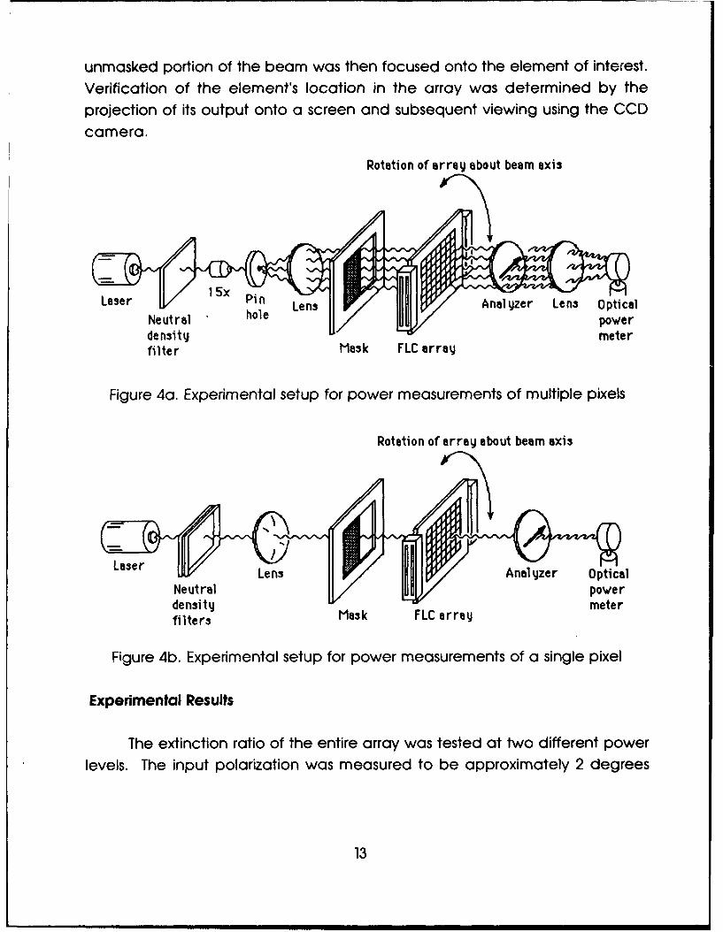
unmasked portion of the beam was then focused onto the element of interest.
Verification of the element's location in the array was determined by the
projection of its output onto a screen and subsequent viewing using the CCD
camera.
Rotation of array about beam axis
aser 1 5x Pin Lens •Analyzer Lens OpticalNeutral hole powerdensity meterfilter Mask FLC array
Figure 4a. Experimental setup for power measurements of multiple pixels
Rotation of array about beam axis
AnLen Alal yzer OpticalNeutral powerdensity M3k FCarymeterfilters Mask FLC array
Figure 4b. Experimental setup for power measurements of a single pixel
Experimental Results
The extinction ratio of the entire array was tested at two different power
levels. The input polarization was measured to be approximately 2 degrees
13

and the SLM was oriented at 7.9 degrees below the horizontal. Table 2 belowlists the analyzer position yielding the largest extinction ratio for the two tests.
The ratio was relatively unchanged, even though the input power for one
sampling was almost twice that of the other. The graphs of output versus
analyzer angle show how the throughput depended on the analyzer's
Power (in pW)Inntpm Analzergn" Maximum Merum E
_ 655.0 p.W 93m 353.9 8.1 43.7
>350.8 ItW 92m 278.9 6.5 42.9
Table 2. Extinction ratios of entire SLM array at 1320 nm
orientation. These graphs demonstrate how the entire SLM did not function as
a perfect half-wave plate.To determine how the overall extinction ratio was dependent on the
individual elements, the throughputs of six elements were tested for their
dependence on the analyzer position. The input polarization was measured
to be at 1.5 degrees and the SLM was oriented at 0 degrees for all six tests.Table 3 lists the extinction ratios of the six elements at the analyzer settings near
and at throughput maxima. Note that for these six elements, there was littlevariation in the opi!:,ncl analyzer orientation; the adjustments needed to
maximize the throughput were within a degree.
In addition, note that if or- - -orrected for 7.9 degree difference in the SLM
orientation that existed for the global test, the location of the throughputmaximum would also have been near 100 degrees. The dependence of theoutput on analyzer position for each of the tested elements is revealed in the
14
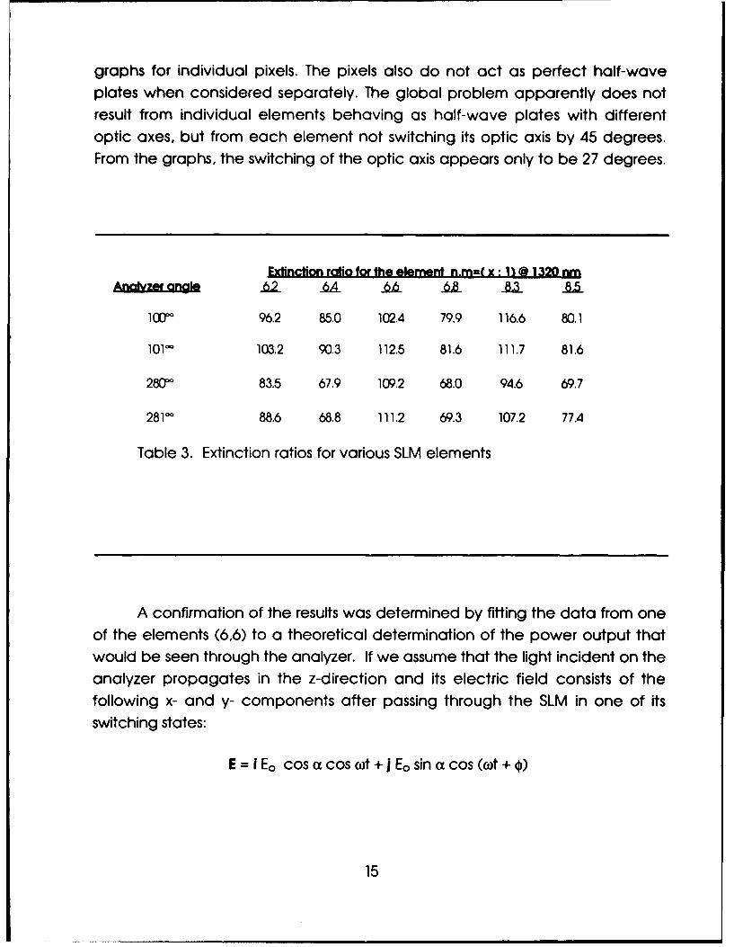
graphs for individual pixels. The pixels also do not act as perfect half-waveplates when considered separately. The global problem apparently does not
result from individual elements behaving as half-wave plates with differentoptic axes, but from each element not switching its optic axis by 45 degrees.From the graphs, the switching of the optic axis appears only to be 27 degrees.
Extinction ratio for the element n.m=( x: *1 @ 1320 ryn
Analyzr oog6 _&U U _
10c[ 96.2 85.0 102.4 79.9 116.6 80.1
1010 103.2 90.3 112.5 81.6 111.7 81.6
280' 83.5 67.9 109.2 68.0 94.6 69.7
2810 88.6 68.8 111.2 69.3 107.2 77.4
Table 3. Extinction ratios for various SLM elements
A confirmation of the results was determined by fifting the data from one
of the elements (6,6) to a theoretical determination of the power output thatwould be seen through the analyzer. If we assume that the light incident on the
analyzer propagates in the z-direction and its electric field consists of thefollowing x- and y- components after passing through the SLM in one of itsswitching states:
E = I Eo cos a cos t + j Eo sin a cos (cot +)
15

where a is the angle the incident polarized light makes with the optic axis and
* is the phase shift in the y-component introduced by the SLM, then the resulting
power that will be read by the optical power meter can be calculated by the
following relation.
P = ( (1 E cos a cos t + j E sin c cos (cot + 0)) ( i cos e + j sin 0•) 2
where 0 is the analyzer angular position and the expression ( I cos 0 + j sin 0) is
the rotational operator on the power P. Simplifying this equation, taking into
account that the power meter can only measure time average responses,
yields:
P =(c E2 (1 + cos 2a cos 20 + sin 2a•sin 20 cos )
If we consider the SLM in its other switched state, i.e. we introduce rotation 8 inthe optic axis, the light passing through the SLM will undergo a rotation of 2&. In
that case, the power read by the meter will be:
Pswitch = ( C E2 (I + cos 2(a + 25) cos 20 + sin 2(a + 25) sin 20 cos ( + 25))
For the case of element 6,6, by choosing a = 10 degrees, 0 = 12 degrees,
8 = -28 degrees, and adjusting the amplitude, the graphs of the theoretical
output are produced. Comparison with .the graph of the data obtained for
element 6,6 shows that this calculation accurately predicts the measured data.
Similar fits could be made for the other elements and the entire array in order
to determine the rotation of the optic axis induced by the switching voltage
and the phase shift occurring in the beam that results from its passage throughthe SLM.
16

Aluminum Oxide Tunneling AND Gate 8
Tunneling Junction
We have fabricated and tested several photon assisted tunnelingdiodes. The devices consisted of a 0.5 mm wide aluminum strip vacuumdeposited on a glass substrate. The aluminum strip was deposited through amask. The aluminum film was oxidized in ambient air. Silicon oxide (SiO)insulating edge protection layers were deposited through a mask onto theedges of the aluminum strip.
Edge protectors
Oxidized Aluminu
Glass Substrat
Copper Contact . .:". ': ':
Z Transparent AluminumContacts
Figure 5. Tunneling diodes structure.
17

Thin strips (80 A)of aluminum were vacuum deposited across the
oxidized aluminum strip with edge protectors as shown in Figure 5. These top
aluminum contacts are thin enough to be transparent to light. Copper contactswere deposited on the thin aluminum strips on either side of the oxidized
aluminum strip.The edge protection prevents shorting at the edges of the bottom
aluminum strip. We measured the tunneling current. All tunneling currents
measured were of the order of a few microamperes. These values are too
low for practical applications. The oxide layers on all devices fabricated were
much too thick causing very low values of tunneling currents. However, we
were able to observe an increase in the tunneling current by about 5% with
illumination from a HeNe laser. The signals obtained were rather small. The
reason for this is that 98% of the light is reflected and only 2% is absorbed by the
device and that the oxide layer was very thick. The light absorption can greatly
be increased by using an anti-reflection coating. Since the device is made out
of a metal a standard anti-reflection coating could not be used. However, an
etalon consisting of a thin transparent film polystyrene layer coated with a 50Aaluminum layer was tried. Light absorption increased by a factor of about ten
with the use of the etalon. However, the thick oxide layer still limited the
tunneling current.The energy diagram of the tunnel barrier is shown in Figure 6. The barrier
potential at a metal insulator junction actually extends into the insulator beyond
the metal. The barrier potential is equal to the energy required to remove an
electron from the metal. Since a metal acts as a very good mirror for
electromagnetic phenomena, including light, the electron that is being
removed from the metal experiences a force due to an effective image
charge in the metal. The potential energy of the electron, due to the image
charge, increases with distance from the metal as is illustrated by the solid
potential barrier curve near each metal in Figure 6. The overlap of these
potential barrier curves from both metals form the actual potential barrier of the
tunnel junction.
18

Energy Idealized
BarrierPotential
, ,• ActualBarrierPotential
S : T• ! Applied
Position
Metal Insulator Metal
Figure 6. Metal-Insulator-Metal tunnel junction.
Photon Assisted Tunneling Transistor
Since the late 1950s various attempts have been made to fabricateTunneling Transistors. This device consists of a thick metal emitter, a 30 - 50A thickinsulating oxide layer, a thin (20 - 100 A thick) metal base, another 30 - 50 A thickinsulating oxide layer, and a metal collector electrode. This is a Metal, Oxide,Metal, Oxide, Metal (MOMOM) device. Such a device could be vc.ry fastsince the quantum mechanical tunneling process is very fast. The quantummechanical tunneling current can theoretically be switched in a few fsec.However, capacitive effects will limit the speed of a practical device. To dateno successful MOMOM transistor has been built. The reason these devices didnot work is that if the metal film that forms the base is thick enough to conducthorizontally, it will be too thick for electrons to penetrate the film from insulator to
19

Light Inpu/ -OxideSlayer
Thin collector metal layer
V Ultrathin
Output metalS~film
R baseEmitter metal layer
Figure 7. Schematic of a Photon Assisted Tunneling Transistor (PATT).
insulator. The electrons are scattered in the metal. It is possible to make verythin metal base layers (10-20 A), however, such layers don't conducthorizontally.
As an alternative to the diode structure, we plan to build MOMOMdevices with exceedingly thin metal base layers only 10 - 20 A thick. We plan toaccess these layers optically through a thin (100 A thick) collector electroderather than trying to make electrical contact to them. The bottom emitterelectrode is made out of a different metal than the base and collectorelectrodes. This generates a built-in potential difference between the emitterand base electrodes. When such a junction is illuminated, an additionalphotovoltage is developed between the emitter and base electrodes. Thisphotovoltage can be used to control the tunneling current from emitter throughthe ultra thin base to the collector. We are still hoping to try to build a PhotonAssisted Tunneling Transistor (PATT). Two of these devices can be connected in
20

series to form a Photon Assisted Tunneling AND Gate. This work is being
continued under another in-house effort (JON 4600P206), Optical Interconnects.
Laser Beam Analysis System
The design, specification, and procurement of the Laser Beam Analysis
System (LBAS) has created a state-of-the-art image capture and processing.
The system was designed and assembled by J. D. Smith with technical
assistance from Mr. Wesley Foor.
The system consists of a lead selenide camera with visible to near-IR
sensitivity whose video output is fed into a Quadra 900 computer via a
NTSC/RS170 compatible video frame grabber. The capabilities of the LBAS
include rudimentary laser beam profiling, surface analysis of optical elements
through relative measurement techniques, and optimization of optical
alignment. The camera is sensitive in the regions above that of CCDs, namely1.0 itm. The LBAS is limited to use in low power (< 1000 itW/cm 2), continuous
wave (CW), visible to near-IR (X < 2.1 t4m) wavelengths. Affordable
commercial beam profiler systems are limited with respect to post-image
capture processing and flexibility of analysis. The system was delivered in
March 1992, with minor CPU RAM upgrades to enhance the run-time
performance of the system.The complete system capability has provided image capture and
analysis for the FLC SLM experiments described in this report. The system
played a key role in a project involving surface analysis of optical coatings
subjected to micrometeor impacts while onboard a communications satellite.
The system will continue to be used for tasks affiliated with Automated Optical
Target Recognition and will continue to be improved in coming fiscal years.
21
Optical Waveguides and Waveguide Lasers
Planar and Ridge Waveguides
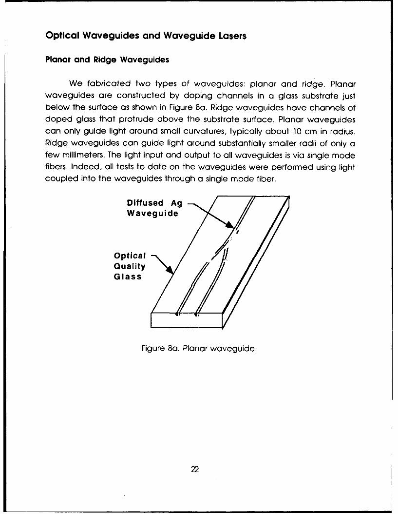
We fabricated two types of waveguides: planar and ridge. Planarwaveguides are constructed by doping channels in a glass substrate just
below the surface as shown in Figure 8a. Ridge waveguides have channels ofdoped glass that protrude above the substrate surface. Planar waveguidescan only guide light around small curvatures, typically about 10 cm in radius.Ridge waveeguides can guide light around substantially smaller radii of only afew millimeters. The light input and output to all waveguides is via single modefibers. Indeed, all tests to date on the waveguides were performed using lightcoupled into the waveguides through a single mode fiber.
Diffused AgWaveguide
OpticalQualityGlass
Figure 8a. Planar waveguide.
22

Ag DiffusedWaveguide
OpticalQualityGlass
Figure 8b Ridge waveguide.
Waveguide Application
Optical waveguides have many applications including pulsemultiplexing and demultiplexing networks. A multiplexing network consists of asingle input waveguide that branches into a number of waveguides. Eachwaveguide branch has a different optical path length. The waveguides arethen recombined. The differences in the optical path length are integermultiples of the shortest path length difference. Consider a pulsed opticclsignal with a repetition rate longer than the longest difference in optical delay.Each path delays the pulse by a different time interval. When the delayedpulses are recombined, a signal with a much higher pulse repetition rate results.The realization using a single glass substrate results in the construction of precisedelays. Also, since all the delay elements are located on the same substrate,they expand and contract with temperature uniformly.
However, to make such a device useful, the pulses have to be not onlydelayed but also modulated. Therefore, each path must also contain amodulator capable of switching the pulse that runs through the particularwaveguide guide on and off. These modulators can be fabricated by eitherdepositing ZnO on the waveguide and patterning the ZnO into a Mach-Zehnder interferometer modulator configuration or attaching a LiNbO 3 Mach-Zehnder modulator onto the waveguide. Since both LiNbO 3 and ZnO have
23
substantially higher indices of refraction than glass, the light will switch from the
glass into the ZnO or LiNbO 3.
Wavegulde Fabrication
The waveguide is fabricated by doping channels in the surface ofoptical quality glass with silver. Silver increases the index of refraction of theglass. Thus, light will be confined to the doped channels in the glass. Since theincrease of the index of refraction in the waveguide region is small, only about0.1% to 0.05%k, the light will be weakly guided. This restricts the curvature of the
guides to large radii. On the other hand, since there are large regions on thesides of the waveguides where the light intensity decreases exponentially, it iseasy to construct evanescently coupled waveguides.
The doping was accomplished as follows: a chromium metal film wasvacuum deposited on the glass substrate. A layer of photoresist was
deposited on the chromium film. The photoresist was exposed through a maskand developed. This left photoresist everywhere except where thewaveguide would be. The chromium film was next etched away from thewaveguide pattern. Next a silver metal film was vacuum deposited on thechromium film leaving the silver film in contact with the substrate where thewaveguide would be. Finally, chromium metal films were vacuum depositedboth on the top and bottom of the glass substrate with the top chromium filmcovering the silver film. Electrodes were attached to the chromium films. Avoltage of about 10 Volts was applied between the chromium film electrodeswhile the substrate was heated to 350 0C for 2 hours. During this process thesilver diffused into the glass forming a channel with a higher index of refractionthan the surrounding glass. This process is known as electric field assisteddiffusion. After the diffusion process was completed the chromium film wasetched off resulting in a planar waveguide.
Ridge waveguides are made by first fabricating a planar waveguide.Photoresist is, again, deposited on the glass substrate. The photoresist isexposed through a mask covering the waveguide, and developed. Themask is aligned with the waveguide using alignment marks. This leavesphotoresist on the waveguide. The glass substrate is etched using HCI in H20 in
24
a 1:4 ratio for one hour. This is followed by etching in a 1: 15 HCI solution in H20 for
5 minutes to smooth the waveguide edges. Lastly, the remaining photoresist isremoved leaving an elevated ridge waveguide on the glass substrate. The air
boundary of the ridge waveguide in conjunction with the silver dopingprovides stronger guiding than is possible in a planar waveguide. The ridgewaveguides will guide light around much smaller radii of curvature than planarguides can.
Wavegulde Measurements
To measure the performance of the waveguides, both ends of the
substrates were polished to provide flat smooth input and output surfaces. Weattached single mode fiber to the single leg of the 'Y". The fiber was used tocouple in light from a low power HeNe laser source. We observed the otherend of the substrate with a CCD camera connected to an IBM PC computer.The computer generated three-dimensional plots of the light intensity as a
function of position 9 . The patterns produced by both the ridge and planarwaveguides were distinct, approximately Gaussian beam profiles. Thewaveguides successfully preserved the characteristics of the input laser beam,validating the fabrication techniques.
Wavegulde Lasers
We are currently fabricating single waveguide and coupled waveguidelasers for use in active optical circuits. The bandwidth of fiber communication,
at present, is limited by the electro-optic input and output devices. Passivewaveguide circuits can be used to multiplex low speed parallel electronicsignals into high speed serial optical signals. Waveguide lasers can be used as
optically activated optical switches in demultiplexing networks. These networksconvert a high speed optical input to low speed parallel optical outputs thatcan then be detected by low speed electro-optic sensors.
Instead of passive optical quality glass, we used glass which was doped
with active laser atoms such as Nd, Er, and Pr as the substrate material of the
waveguide lasers. The first waveguide lasers are fabricated out of optical
25

quality Nd doped glass. The Ag doped waveguides are fabricated using thesame technique as the glass waveguide. Both planar and ridge waveguides
are being used. The lasers use external dielectric layered mirrors. Both deviceswith vertically polished ends and with ends that are polished at the Brewster
angle are being fabricated. The Brewster angle laser ends provide lessreflection by the boundary for polarized light than straight ends do. However, it
is harder to attach mirrors to the Brewster angle faceted waveguides. Thesingle waveguide lasers have a waveguide that has a slight S-curve to guide
only low order modes. A planar waveguide laser is shown in Figure 9. Higher
order modes will be radiated in the curving section of the waveguide.
ExternalDielectr Mirrors
Diffused Ag
Waveg uide-
Glass dopedwith lasing
ions
Light Outpu
Figure 9. Single waveguide laser with external mirrors.
There are several methods of pumping these lasers. The first method we
plan to use is to pump the waveguide lasers from the top as shown in Figure 10.
26

The substrate is illuminated from the top by a gas discharge lamp. In order to
minimize heating of the waveguide laser, the light from the gas dischargelamp is dispersed by a prism. Light with different wavelength X is dispersed in
different directions by the prism. A prism and a slit are used to select theappropriate pumping wavelength from the gas discharge lamp. Only the lightwith the desired wavelength for pumping passes through the slit and illuminatesthe waveguide. Light at other wavelengths is blocked by the shield.
, Curved Mirror
\ I
Gas DischargeLamp
Pump light I ,..\ /.Light atat correct undesiredwave..en gt.•-- wavelength
Shield with slit - \, _W aveguide
\-wavguidelaser
Figure 10. Laser pumping by direct illumination.
Another method of pumping the laser is to use a diode laser that
radiates at the correct pumping wavelength. The light from the diode laserpropagates collinearly with the signal light. The waveguide laser is illuminatedthrough one of the :fiel-ctric mirrors. The dielectric mirrors only reflect light at the
signal light wavelength, since they are relatively transparent at other
wavelengths.
27
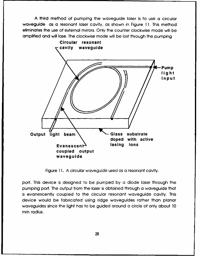
A third method of pumping the waveguide laser is to use a circular
waveguide as a resonant laser cavity, as shown in Figure 11. This method
eliminates the use of external mirrors. Only the counter clockwise mode will beamplified and will lase. The clockwise mode will be lost through the pumping
Circular resonantcavity waveguide
Pumplight
Sin p u t
Output light beam _ Glass substratedoped with active
Evanescen lasing ions
coupled outputwaveguide
Figure 11. A circular waveguide used as a resonant cavity.
port. This device is designed to be pumped by a diode laser through the
pumping port. The output from the laser is obtained through a waveguide thatis evanescently coupled to the circular resonant waveguide cavity. This
device would be fabricated using ridge waveguides rather than planarwaveguides since the light has to be guided around a circle of only about 10
mm radius.
28

Coupled Wavegulde Lasers
Our ultimate goal is the fabrication and testing of coupled waveguide
lasers. A Y-cavity coupled waveguide laser is shown in Figure 12. These devices
have contacts so that an electric field can be applied across the
waveguides. The wavelength of one of the outputs can be shifted with respect
to the other output by the application of a voltage to the contacts. The
application of an electric field across one of the waveguides shifts the energy
levels of the active lasing ions in that waveguide. The shift of energy levels by
an electric field is known as the Franz Keldish effect. The Franz Keldish effect
shifts the gain curve of the laser branch that has a bias applied causing it to
oscillate at a slightly different wavelength than the other branch of the laser.
Dielectric Mirror•
Ag dopedWaveguide-
Glass substratedoped with activelasing ions
•/Z• •.Electrical
•• contacts
Output light beams
Figure 12. Y-type waveguide coupled lasers.
29
This device can be used in heterodyne optical processors where light
waves differ in frequency by microwave or millimeter (mm) wave frequencies.
This is often accomplished with acousto-optic cells. However, acousto-optic
cells are limited to frequencies below about 1 GHz. The coupled lasers are
theoretically able to provide frequency differences of up to about 100 GHz.
The frequency difference is adjusted with the electrical bias applied across thewaveguides.
Other configurations of coupled waveguide lasers are possible. One
can, for example, use two evanescently coupled waveguides for this
application.
30

Artificial Optical Delay Une 10
The Artificial Long Delay Optical Processor (ALDOP) generates a large
variable delay of a band limited pulse modulated RF signal. The proposed
prototype ALDOP has potential use in a Passive Radio Ranging (PRR) system
operating in the 82.5-97.5 MHz frequency band. The complete system will
combine a passive electronic band pass filter with the optically based ALDOP
to impart a unique phase shift to each frequency component of an incoming
RF signal. The phase shift is generated using optical heterodyne methods that
incorporate the transmission and modulation of light through a series of optical
components including an acousto-optical cell and a Fresnel Zone Plate.
System Description
The generation of RF signals with long variable delays is difficult to
achieve with great accuracy in purely electronic based systems. It has been
demonstrated that optical systems are more suitable for achieving precise
delays using optical heterodyne techniques11 . One application of an ALDOP is
in a prototype Passive Radio Ranging (PRR) system 12 that operates at 82.5-97.5
MHz. The corresponding fractional RF bandwidth of 16.667 % is centered at 90
MHz. This particular frequency range is chosen for two reasons: 1) local FM and
TV broadcast stations provide convenient RF illumination of targets in this
frequency range, and 2) acousto-optic (AO) cells driven by RF signals in the
62.5-77.5 MHz range are readily available. The corresponding fractional
bandwidth of 21.429 % is centered at 70 MHz. The optical processor provides
the 62.5-77.5 MHz broadband local oscillator (LO) for this system.Consider a signal S1 with fl =100 MHz propagating a distance of 5 km
from a target to an antenna, while a signal S2 with f2 = 80 MHz is traversing the
same distance. The signals will undergo phase shifts of 01=10479.225 radians for
S1 and 02 =8383.380 radians for S2. The optical processor has to compensate for
signals with phase shifts between •j and •2.
31

_Passivebad
Iter'I Trigger
OPTICAL PROCESSOR
Figure 13. Schematic of the Artificial Long Delay Optical Processor.
The ALDOP functions as follows: a band limited electronic signal isproduced by passing a periodic pulse modulated RF (or microwave) signalthrough a passive electronic band pass filter. The output is a continuous signal
whose frequency components are limited by the pass band of the filter. Thefilter produces a signal for a time on the order of several milliseconds after theinput pulse has ceased to exist. Therefore, the storage of the signal during therelatively long delay actually occurs within the filter. The output is used as the
driving signal for an AO cell whose characteristic bandwidth and center
frequency are matched to the filter.
Optical Processor
The optical processor shown in Figure 14 utilizes the optical heterodynetechniques of Toughlian and Zmuda 11 . A HeNe laser beam is split by a non-polarizing beamsplitter into reference (we) and signal beams. The AO cell shiftsthe laser beam proportionally to the frequencies of the RF signal (filter output)
which translates into an angular spread. The measured spread at the output ofthe IntraAction model AOD-70 AO cell used in this experiment was 2.4375 mRad
(=0.1396580) for a bandwidth of 15 MHz centered at 70 MHz.
32

Laser Mirror
Sgal beam '
Optic Cell RF signal
450Pim Zone Plate Expande
Ti 45° Prism • a
Tiltingco+ 0Ua
Min-or °
I Photo
Detector
2F 2F ,.I
Figure 14. Detail of ALDOP.
The tilting mirror allows for adjustment of the incidence angle a of the light
beam to the prism to vary the magnification of the angular spread of the light
beam exiting the prism. A 450 prism made from Schott BK-7 glass with an indexof refraction n= 1.51509 at X=632.5 nm is used to increase the angular spread to amaximum of 1.2793710. Portions of the beam (denoted o0 0+(ORFmax and
)O+O'RFmin in Figure 14) that are shifted by different RF drive frequencies will
emerge at different angles from the prism.A Fresnel Zone Plate (FZP) with a zero order focal length F is used to focus
the spreading light beam. Different phase shifts are produced by the variation
in optical path length through the FZP. The arrangement of the prism and FZP isdesigned to generate the largest phase shift of the light beam shifted by thehighest RF frequency (CORFmax).
Since the optical path length differences are large compared to lightwavelengths, it is possible to obtain very large phase shift differences. Eachbeam incurs a phase shift OORF) :
33

4F IRF X cos(y - J)
where 03 is an offset angle and where we neglected the path from the AO cellto the output of the prism. We assume that the spread of the light beam fromthe AO cell is small compared to the spread of the light beam after the prism.The output angle y is related to the incident angle a of the prism input beam bythe following relation:
s iy [4^ 7 -sin7 2 - sincx] (2)
The angle ax is related to the exit angle y of the prism output beam by a similar
relation:
sina= [ n - sin'y- sinyl (3)
In both equations, n is the index of refraction. The largest magnification of theangular spread by the prism will occur when y = 90', corresponding to anincident angle ao= 5.6080. The prism is adjusted in such a way that when the
tilting mirror is at the maximum gain position, the light beam shifted by thelargest signal frequency (co0+)'RFmax) emanates from the prism with an angle
7=900.
The delay t- d'(fRF) is the change of the phase 4 (fRF) with frequencydfRF
fRF One can obtain an expression for - by substituting eq. (2) for y into eq. (1)and differentiating the resulting expression with respect to the frequency fRF"
4F sin(y - P) sinycosci I dctCOS2(y cosy -2 d12 (4)
where•=c +a•. (5)3 mirror
34
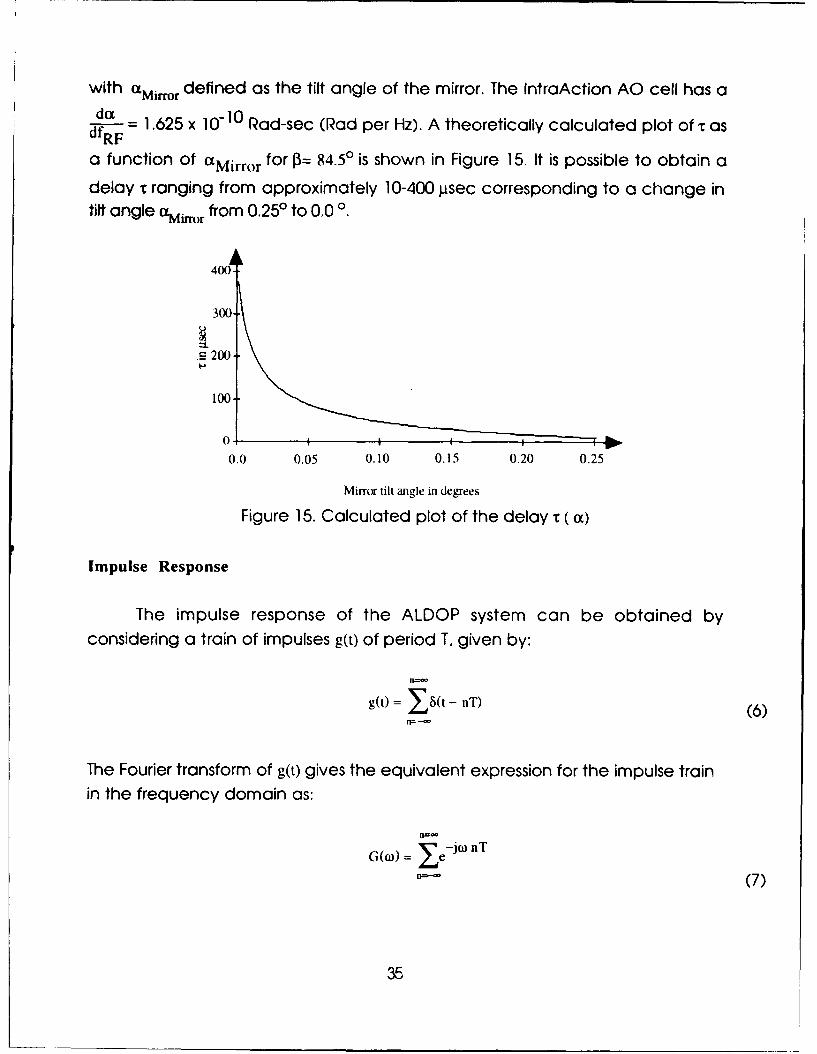
with aMirror defined as the tilt angle of the mirror. The IntraAction AO cell has a
da = 1.625 x 10- Rad-sec (Rad per Hz). A theoretically calculated plot of t asdfRF=1.2x1a function of a0Mirror for 3 = 84.50 is shown in Figure 15. It is possible to obtain adelay T ranging from approximately 10-400 psec corresponding to a change intilt angle aMifmr from 0.250 to 0.0 0.
400
300
.C- 200-
100-
0 - - i -- - - -
0.0 0.05 0.10 0.15 0.20 0.25
Mirror tilt angle in degrees
Figure 15. Calculated plot of the delay (a)
Impulse Response
The impulse response of the ALDOP system can be obtained byconsidering a train of impulses g(t) of period T, given by:
Ni--
g(t) = I 8(t- nT) (6)
The Fourier transform of g(t) gives the equivalent expression for the impulse trainin the frequency domain as:
G(64) =-en (7)
35

Each frequency component is shifted by a phase wt proportional to thefrequency o:
fi-
n ,o -j)( nT - T)
By taking the band limited inverse Fourier transform we obtain:
h() = don-=- - (9)
where (oc is the center frequency of the bandwidth Bw. Evaluating the integral
of Eq. 9 yields the transfer function h(t) of the Artificial Long Delay Optical
Processor.:
o) B
2B' i wn - - jo(t -twh(t) = c wl 2 e
-- W(nT - - 0) (10)2
where t is the delay generated by the optical processor (see Eq. 4). Indeed, it
should be possible to obtain delays as large as 400 lisec, corresponding to a
detection range of 119.916 kilometers for the PRR system.
36
Conclusions and Recommendations
FLC Spatial Light Modulator
The tests of the individual elements and the entire SLM array demonstrate
how the device has not been optimized for operation at 1320 nm. The data
from the elements that were tested suggest that the optic axis fails to switch 45
degrees when the voltage is switched. Investigation of the dependence of
the rotation of the optic axis on the voltage supplied to the elements may
reveal that the voltage being applied has not been optimized for operation
at 1320 nm. Another factor that needs to be investigated is the dependence of
the thickness of the FLC layer on the switching of the optic axis. The current
thickness may not be ideal for 1320 nm light.
The overall assessment of the SLM was that it is not optimal for the
intended application where it would be used to independently switch 25
spatially separated laser beams. The switching requirement would easily be
satisfied by the manufacturer's design of the controller, driver, and software, but
the need to rotate the array to maximize the throughput for each element
disqualifies the array as a candidate for the modulation of the low power laser
beams in the system. The variation in contrast ratio among individual pixels at a
fixed angle indicates that the throughput of some elements would not be
maximized without rotation of the array. The SLM is generally used with a laser
beam of sufficient power so that the reduced throughput would not adversely
affect the dynamic range of a detection system. In this application, the
decreased throughput that will result in the pixels that are not oriented at their
maximum would cause detection of the low power laser beams to be close
to the noise level of a photodetector.
Active Optical Waveguide Circuits
Dr. Kornreich is currently pursuing the development of waveguide laser-
based active optical circuits. This technology seems to offer more possibilities
than was anticipated when this task started. As previously stated, one of the
main limitations of the speed by which data can be transmitted over optical
37
fibers is the relatively slow response of electronic circuits. Electronic lightmodulators and detectors are currently limited to about 20 to 30 GHz while
optical fibers have a bandwidth of 1014 Hz. Active optical circuits using coupledwaveguide lasers can, theoretically, switch in about 50 fsec. Such devices can
be used to convert 'slow* parallel electronically generated optical signals to"fasto serial optical signals that are then transmitted over a fiber. The high speed
serial optical signals from the fiber are then converted to lower speed optical
parallel signals using active waveguide circuits. The low speed optical parallelsignals can than be detected electronically. Dr. Kornreich hopes to have an
active waveguide circuit working by the end of 1993. The work started here wastransferred to another in-house project for the remainder of FY93.
For some time people were trying to fabricate light emitting devices on
silicon Integrated Circuits (ICs). Several approaches have been tried. One
approach is to mount light emitting devices made out of other semicon-ductors such as GaAs on silicon ICs. However this is a very tedious process.Another approach is to fabricate light emitters in the silicon itself. This requiresvery high current densities which result in large power consumption and high
temperatures.Fabrication of optical waveguide circuits on silicon ICs has recently been
proposed (not by Syracuse University). Such devices can be fabricated by
Chemical Vapor Deposition (CVD) processes on silicon substrates. The CVDprocess differs little from other CVD processes already in use in silicon IC
fabrication. The fabrication of optical waveguide circuits on silicon ICs for thefirst time allows the integration of the highly developed silicon technology with
high speed active optical circuits. Dr. Kornreich highly recommends that the
active optical waveguide circuit technology be further developed.
Electro-Optic Tunneling Devices
The results of the work with the various Metal-Oxide-Metal tunneling
devices was less successful. Even though this technology is theoreticallypromising, it was not possible to construct useful devices to date. It is Dr.
Kornreich's opinion that there is no fundamental theoretical limitation that states
that such devices could never be produced. While working with the tunneling
38

devices it was concluded that a substantially larger effort than this program
allowed would be required to achieve any success. The light assistedtunneling transistor is an interesting device. This technology will require muchmore research before any practical devices can be fabricated.
Artificial Optical Delay Line
The work with the Artificial Optical Delay Line was hampered by an
extensive time lag in the delivery of the Fresnel Zone Plate. The experiment was
continued on a part-time basis by Dr. Kornreich. The technical paper
describing the ongoing work is currently in progress and should be released bythe end of the summer of 1993. It is not recommended that this work be
continued under the branch in-house efforts. The proof of concept was
realized but did not meet expectations.
39

References
1 C.L. Wang, J.T. Tung, J.D. Smith and P. Kornreich, "CdTe-lnSb nonlinear etalonswitch',SPIE Proceedings, Vol. 1790, pp 126-9, Sept 1992.
2 P. L. Gouley and T. J. Drummond, 'Optical bleaching in an epitaxial (Al, Ga)As Fabry-Perot Resonator,' App/. Phys. Lett., Vol. 51, pp. 1395-1397, 1987.
3 T. H. Wood, C.A. Burrus, D.A.B.Miller, D. S. Chemla, T. C. Damen, A. C. Gossardand W. Wiegmann, '131 ps optical modulation in semiconductor multiplequantum wells', IEEE Jour. of QE, Vol. QE-21, pp. 117-118, 1985.
4 D. A. B. Mill ,r, D. S. Chemla, T. C. Damen, T. H. Wood, C.A. Burrus, Jr., A. C.Gossard, ar J W. Wiegmann, 'The quantum well self-electrooptic effectdevice: Optoelectronic bistability and oscillation, and self-linearizedmodulation', IEEE Jour. of QE, Vol. QE-21, pp. 1462-1476, Sept. 1985.
5 A. L. Lentine et al., 'Multistate self-electrooptics effect devices', IEEE Jour. ofQE, Vol. QE-25, pp1921-1927, Aug. 1989.
6 D. Stanchfield and J.D.Smith, 'Measurement of Contrast Ratios for a
Ferroelectric Liquid Crystal Spatial Light Modulator', 1993, publication pending.
7 D. Stanchfield, P.G. Kornreich, J.D. Smith, Measurement of Contrast Ratios fora Ferroelectric Liquid Crystal Spatial Light Modulator, Rome Laboratorytechnical report # RL-TR-91-404, Air Force Systems Command, Griffiss Air ForceBase, NY 13441-5700. Dec 1991.
8 P.G. Kornreich, 'Analysis of Devices for Pulse Position Modulation Networks',Final Report, publication pending : Rome Laboratory technical report, Air ForceMateriel Command, Griffiss Air Force Base, NY 13441-5700. Dec 1991.
9 See Figures 3 and 4 of Reference 8.
10 P.G. Kornreich, J.D. Smith, Artifical Long Delay Optical Processor, SPIEProceedings, Vol. 1790, pp 130-2, Sept 1992.
11 E. Toughlian and H. Zmuda, 'A Photonic Variable RF Delay Line for PhasedArray Antennas', IEEE Journal of Lightwave Technology, Vol. 8, No. 12, pp. 1824-1828, 1990.
12 N.H. Farhat, 'Principles of Broad-Band Coherent Imaging%, Journal of theOptical Society of America, Vol. 67, No. 8, pp. 1015-1021, August 1977.
40

MLSNZON
OF
ROME LABORATORY
Rome Laboratory plans and executes an interdisciplinaryprogram in research, development, test, and technologytransition in support of Air Force Command, Control,Communications and Intelligence (C31) activities for allAir Force platforms. It also executes selectedacquisition programs in several areas of expertise.Technical and engineering support within areas ofcompetence is provided to ESC Program Offices (POs) andother ESC elements to perform effective acquisition ofC31 systems. In addition, Rome Laboratory's technologysupports other AFMC Product Divisions, the Air Force usercommunity, and other DOD and non-DOD agencies. RomeLaboratory maintains technical competence and researchprograms in areas including, but not limited to,communications, command and control, battle management,intelligence information processing, computationalsciences and software producibility, wide areasurveillance/sensors, signal processing, solid statesciences, photonics, electromagnetic technology,superconductivity, and electronicreliability/maintainability and testability.