Rights / License: Research Collection In Copyright - Non ...27640/... · for multiple antenna...
190
Research Collection Doctoral Thesis Active antenna radio frontends for multiple antenna communication systems Author(s): Brauner, Thomas Publication Date: 2004 Permanent Link: https://doi.org/10.3929/ethz-a-004904237 Rights / License: In Copyright - Non-Commercial Use Permitted This page was generated automatically upon download from the ETH Zurich Research Collection . For more information please consult the Terms of use . ETH Library
Transcript of Rights / License: Research Collection In Copyright - Non ...27640/... · for multiple antenna...

Research Collection
Doctoral Thesis
Active antenna radio frontends for multiple antennacommunication systems
Author(s): Brauner, Thomas
Publication Date: 2004
Permanent Link: https://doi.org/10.3929/ethz-a-004904237
Rights / License: In Copyright - Non-Commercial Use Permitted
This page was generated automatically upon download from the ETH Zurich Research Collection. For moreinformation please consult the Terms of use.
ETH Library

ACTIVE ANTENNA RADIO FRONTENDS
FOR MULTIPLE ANTENNA
COMMUNICATION SYSTEMS
rece
iver
rece
iver
rece
iver
rece
iver
LO
IF1 IF2 IF3 IF4
attenuator
CAL2CAL1 linecalibration
Thomas Brauner
DISS. ETH No. 15642


DISS. ETH No. 15642
ACTIVE ANTENNA RADIO FRONTENDSFOR MULTIPLE ANTENNA
COMMUNICATION SYSTEMS
A dissertation submitted to theSWISS FEDERAL INSTITUTE OF TECHNOLOGY
ZURICH
for the degree ofDoctor of Technical Sciences
presented byTHOMAS BRAUNER
Dipl. Ing., RWTH AachenBorn February 8, 1973
in Koln (Germany)
accepted on the recommendation ofProf. Dr. W. Bachtold, examiner
Prof. H. Bolcskei, Prof. R. Kung, coexaminers
2004


Twenty years from now you will be more dis-appointed by the things that you didn’t do thanby the ones you did do. So throw off the bow-lines. Sail away from the safe harbor. Catchthe trade winds in your sails. Explore. Dream.Discover.
— Marc Twain


Contents
Table of contents v
Abstract ix
Zusammenfassung xi
1 Introduction 11.1 Motivation 11.2 Organization of this work 3
2 System design 52.1 Receiver design 5
2.1.1 Dynamic range 52.1.2 Receiver architecture 8
2.2 Multiple antenna system 102.2.1 Noise and linearity 102.2.2 Antenna combining methods 112.2.3 Local oscillator distribution 122.2.4 Antenna placement 13
2.3 Noise in multiple antenna systems 162.3.1 Signal and noise model 162.3.2 Noise correlation 172.3.3 Phase noise 182.3.4 Correlation of phase noise 192.3.5 System noise model 21
2.4 Testbed architecture 21
3 Integrated circuit design 233.1 Process technology 23
3.1.1 Choice of technology 233.1.2 TriQuint TQTRx process 25
3.2 Low-noise amplifier 263.2.1 Input matching 263.2.2 Device scaling 283.2.3 Three-stage amplifier 29

vi Contents
3.2.4 Measurement results 303.3 Downconverter 32
3.3.1 Resistive mixer design 323.3.2 Mixer scaling 363.3.3 Integrated downconverter 373.3.4 Measurement results 37
3.4 Integrated front-end 423.4.1 Architecture 423.4.2 Switchable LNA 423.4.3 Image filter 443.4.4 Layout 453.4.5 Experimental results 47
3.5 Power amplifier 543.5.1 Design 543.5.2 Experimental results 573.5.3 Pulsed operation 58
3.6 10.7–11.7 GHz SiGe downconverter 603.6.1 IBM 6HP SiGe BiCMOS process 613.6.2 Low-noise amplifier 613.6.3 Integrated downconverter 65
3.7 Conclusions 69
4 Passive arrays 714.1 Antenna design 71
4.1.1 Choice of antenna structure 714.1.2 Aperture-coupled patch antenna 724.1.3 Modelling 734.1.4 Design method 744.1.5 Results 76
4.2 Differential antenna 784.2.1 Differential MMIC interface 784.2.2 Design 784.2.3 Measurement results 79
4.3 Antenna arrays and mutual coupling 824.3.1 Non-ideal arrays 824.3.2 Classification 834.3.3 Coupling compensation 854.3.4 Array of aperture-coupled patch antennas 864.3.5 Array coupling model 89
4.4 Reduction of coupling in active arrays 904.4.1 Interface optimization 90

Contents vii
4.4.2 Experimental verification 924.5 Conclusions 95
5 Calibration 975.1 Problem formulation 97
5.1.1 Active circuit variations 985.1.2 Calibration network precision 1005.1.3 Calibration requirements 1015.1.4 Pattern error 1035.1.5 Statistical array error 103
5.2 Existing calibration methods 1045.2.1 Passive array calibration 1045.2.2 Coupling estimation from far-field 1055.2.3 Test-tone calibration 1085.2.4 Hybrid methods 1105.2.5 Improved Hybrid Calibration 111
5.3 Transmission-line calibration method 1125.3.1 Description of method 1125.3.2 Estimation of systematic error 1145.3.3 GaAs Tx/Rx-switch with calibration ability 1185.3.4 Experimental Results 119
5.4 Dynamic transmitter calibration 1225.4.1 Instantaneous error 1225.4.2 Power amplifier 1235.4.3 Array calibration 123
5.5 Conclusions 127
6 Active antenna arrays 1296.1 Linear array 129
6.1.1 Design 1296.1.2 Experimental results 1326.1.3 Calibration 136
6.2 Gain and phase stability 1396.3 Noise correlation 143
6.3.1 Amplitude noise correlation 1436.3.2 Phase noise correlation 144
6.4 Conformal array 1466.4.1 Motivation 1466.4.2 Design 1476.4.3 Experimental results 151
6.5 Conclusions 157

viii Contents
7 Summary, conclusions and outlook 1597.1 System design 1597.2 Integrated circuit design 1597.3 Passive arrays 1607.4 Calibration 1617.5 Active antenna arrays 1617.6 Conclusions and future work 162
Bibliography 163
Curriculum vitae 171
List of publications 173
Acknowledgments 175
Abstract
Goal of the work presented in this dissertation is to implement andcharacterize a 5 GHz active antenna array. Planar aperture-coupled patchantennas and monolithically integrated active circuits are combined toyield a compact, robust and easy-to-manufacture multiple antenna fron-tend. The realized hardware is intended for the use in both, in multipleantenna wireless LAN systems and for a multi-dimensional channel sound-ing equipment.
To enable the application in the measurement system, the frontend isoptimized for low-noise and high linearity. A classical superheterodynearchitecture is chosen to maintain flexibility when adopting the system todifferent environments. An internal calibration signal is provided at allreceiver inputs to determine and compensate all variations of the activehardware.
A commercially available 0.6 µm GaAs MESFET process is used to in-tegrate the complete RF-frontend, including low-noise amplifiers, a lumped-element image filter and downconverter, onto a single chip of 3.2 mm2.Thereby, a state-of-the-art single side-band noise figure of less than 4 dBand an image rejection of more than 35 dB are reached. An active switch-ing concept is proposed to select between receiving and calibration modewithout degrading the noise figure. To evaluate the ability of modernsilicon-based technologies, an 11 GHz receiver frontend is demonstratedon a low-cost 47 GHz SiGe process. Using the MOSFET device to forma resistive mixer, a single-sideband noise figure of 7 dB and a input com-pression point of −14 dB can be realized at the same time.
Through the development of an equivalent circuit model, an efficientdesign of the passive antenna structure for given specifications is facili-tated. The model is heuristically extended to include the mutual couplingbetween adjacent elements. The co-design of the receiver and the antennastructure allows to optimize the common interface. A differential antennainterface and the reduction of mutual coupling by controlling the antennatermination impedance are both experimentally verified.
The realized four element active integrated antenna array reaches anexcellent long-term stability of transmission gain and phase. For a com-
x Abstract
plete receiver system, including conversion to the digital baseband, gainvariations of less than ±0.1 dB are measured over three days in an officeenvironment. These fluctuations are mainly due to changes of the ambi-ent temperature and are similar for all channels. The resulting distortionsof the array pattern, therefore, stay even lower. The dynamic behaviorof the transfer functions is studied for the case of jointly switched poweramplifiers, which experience strong thermal changes due to self heating.It is found, that fast changes are correlated well for the employed mono-lithically integrated circuits. For typical burst lengths up to several mil-liseconds it is demonstrated that no significant pattern error occurs.
On a system level, the noise correlation between the individual chan-nels is studied. Some correlation of the receiver noise was noticed due tocorrelated spurious occurring in the digital receiver part. A small phasedecorrelation with a 1/f -characteristic is found, which is almost negligiblefor most practical applications.
Furthermore, available calibration methods are studied and appliedto the active array. The effect of mutual coupling is removed using aninverted coupling matrix. Over a the range of the element beam-widththe behavior of the calibrated array can be approximated by the simplegeometrical ray-model. A novel transmission line method is proposed,which allows to calibrate the variations of the active circuits without theneed for a precise divider network.
With the help of the new calibration method and the highly integratedfrontend a novel type of conformal active array is demonstrated. Thecircuitry is first assembled in standard planar technology and then bent tothe final shape, which enables a low cost production. Further advantagesof this array are a reduced mutual coupling and a wider angular range ofoperation.

Zusammenfassung
Das Ziel der in dieser Dissertation vorgestellten Arbeit ist die Imple-mentierung und Charakterisierung eines 5 GHz aktiven Antennenarrays.Planare aperturgekoppelte Patchantennen werden mit monolitisch inte-grierten aktiven Schaltungen kombiniert um ein kompaktes sowie robu-stes Antennen-Frontend zu erhalten. Das realisierte Gerat kann sowohlin drahtlosen Datennetzwerken, als auch in einem Messgerat zur mehr-dimensionalen Funkkanal-Charakterisierung (channel-sounder) eingesetztwerden.
Um eine Anwendung im Messsystem zu ermoglichen, ist das Front-end auf niedriges Rauschen sowie eine hohe Linearitat optimiert. Eineklassische Uberlagerungsempfanger-Architektur wurde ausgewahlt um dienotige Flexibilitat sicherzustellen, wenn das System an verschiedene Um-gebungen angepasst werden soll. Die Variationen der aktiven Schaltungenkonnen mit Hilfe eines Kalibrationssignals bestimmt und kompensiert wer-den.
Mit Hilfe eines kommerziell erhaltlichen 0.6 µm GaAs MESFET Pro-zesses kann das komplette HF-Frontend, bestehend aus rauscharmen Ver-starkern, einem Filter zur Spiegelfrequenzunterdruckung aus konzentrier-ten Elementen und einem Frequenzumsetzer, auf einen einzigen Chip von3.3 mm2 Grosse integriert werden. Dabei wird eine state-of-the-art Ein-seitenband-Rauschzahl von weniger als 4 dB, sowie eine Spiegelfrequenz-unterdruckung von mehr als 35 dB erzielt. Ein aktiver Schalter wird vor-geschlagen, um zwischen dem Empfangs- und dem Kalibrationssignal zuwahlen, ohne die Rauschzahl zu verschlechtern. Die Moglichkeiten moder-ner siliziumbasierter Technologien werden mit einem 11 GHz Empfangerauf einem 47 GHz SiGe Prozess demonstriert. Mit der Verwendung desMOSFETs als resistiven Mischer konnen gleichzeitig eine niedrige Ein-seitenband-Rauschzahl von 7 dB, sowie ein hoher Eingangskompressions-punkt von −14 dB erreicht werden.
Durch die Entwicklung einer Ersatzschaltung kann der effiziente Ent-wurf der passiven Antennenstruktur nach gegebenen Spezifikationen ver-einfacht werden. Das Modell wird heuristisch zur Erfassung der gegen-seitigen Antennenkopplung zwischen benachbarten Elementen erweitert.

xii Zusammenfassung
Der gleichzeitige Entwurf von Empfanger und Antennenstruktur erlaubtdie gemeinsame Schnitstelle zu optimieren. Sowohl eine differentielle An-tennenschnittstelle, als auch die Reduzierung der gegenseitigen Antennen-kopplung durch die optimale Wahl der Antennenfusspunktimpedanz wer-den beide experimentell bestatigt.
Die Ubertragungsfunktionen des entwickelten vierelementigen aktivenintegrierten Antennenarrays zeigen eine exzellente Langzeitstabilitat vonPhase und Amplitude. An einem kompletten Empfangssystem, welchesauch die Konvertierung ins digitale Basisband beinhaltet, wird eine Ver-starkungsanderung von weniger als ±0.1 dB uber drei Tage in einer Buro-umgebung festgestellt. Die Anderungen sind hauptsachlich von der Um-gebungstemperatur abhangig und sehr ahnlich fur alle Kanale. Dadurchbleibt der Einfluss auf das Richtdiagramm gering. Das dynamische Ver-halten der Ubertragungsfunktion von gemeinsam geschalteten Leistungs-verstarkern wird untersucht, welche starken Temperaturschwankungen durchSelbsterhitzung unterworfen sind. Es wird festgestellt, dass schnelle An-derungen bei den verwendeten monolithisch integrierten Schaltungen gutkorreliert sind. Es kann gezeigt werden, dass wahrend einer typischenUbertragungsdauer von wenigen Millisekunden keine nennenswerten Feh-ler im Richtdiagramm auftreten.
Auf Systemebene wird die Korrelation des Rauschens auf den ein-zelnen Kanalen untersucht. Ein korrelierter Rauschanteil erscheint, derauf korrelierte unerwunschte Nebenprodukte der Signalprozessierung imdigitalen Empfanger zuruckzufuhren ist. Eine geringe Dekorrelation derUbertragungsphasen mit 1/f -Charakteristik kann festgestellt werden, diejedoch fur die meisten praktischen Anwendungen ohne Bedeutung ist.
Bekannte Kalibrationsmethoden werden untersucht und auf das aktiveArray angewendet. Die Auswirungen der gegenseitigen Antennenkopplungkonnen mit Hilfe einer invertierten Koppelmatrix kompensiert werden.Das Verhalten des kalibrierten Arrays kann innerhalb der Keulenbreiteder Einzelstrahler durch das einfache strahlenoptische Modell angenahertwerden. Es wird eine neuartige Kalibrationsleitungs-Methode vorgeschla-gen, mit welcher die Variationen der aktiven Schaltungen kalibriert werdenkonnen ohne ein prazises Verteilernetzwerk zu benotigen.
Mit Hilfe des neuen Kalibrationsverfahrens und den hochintegriertenHF-Frontend kann eine neue Art von konformen aktiven Arrays demon-striert werden. Die Schaltung wird zuachst in gewohnlicher planarer Tech-nologie hergestellt, um dann in die endgultige Form gebogen zu werden,was eine kostengunstige Produktion ermoglicht. Weitere Vorteile diesesAntennenarrays sind eine geringere Antennenkopplung und ein grossererabgedeckter Winkelbereich.

1
Introduction
1.1 Motivation
The idea of grouping antennas into an array is almost as old as the historyof radio wave transmission itself. The first antenna array reported datesback to 1901. It was designed by Guglielmo Marconi, who intended to useit for his transatlantic wireless communication experiment [1]. Unfortu-nately the two erected arrays at both coasts of the Atlantic were destroyedby strong storms before they could ever be used.
Since the 1950s, antenna arrays are attractive for radar systems [2, 3],where the phased array principle allows to point the antenna beam todifferent positions by changing electrical parameters rather then mechan-ically turning the structure. Due to the high associated costs the use ofthese arrays was mainly limited to military systems and a multitude oftheoretical and experimental works were conducted with this background.
With rapidly growing possibilities of digital signal processing, antennaarrays became attractive for wireless communication systems. Replac-ing the simple non-directive antenna by an electronically controlled beamprincipally offers several advantages:
• For the same link distance, less transmit power is needed. Batterypower and expensive power amplifiers can be saved.
• The higher directivity mitigates multi-path propagation effects. Thischanges the fading properties and reduces the intersymbol interfer-ence.
• Interfering sources can be suppressed by placing pattern zeros intotheir directions.
• It becomes possible to separate signals arriving at different angles.This allows to have several individual communication links simulta-neously and at the identical frequency, as illustrated in Fig. 1.1.
• Additional antennas add diversity and multiplexing gain.

2 Introduction
spatialfilter
signal 2signal 1
user 2
user 1
Fig. 1.1 Smart antenna acting as a spatial filter, separating the signals from
mobile users 1 and 2 at the base station.
Especially for the ability of sharing the radio resources the now- calledsmart antenna was proposed to solve the frequency congestion, which fol-lowed the enormous worldwide success of the digital mobile communica-tion standards like GSM. Motivated by these expectations, several exper-imental systems have been built for the DECT [4,5], the GSM/DCS1800[6, 7] and other standards. Also first commercial products are available.It is concluded that the system capacity can at least be doubled withexisting techniques [8]. The performance is generally limited by the fi-nite suppression of unwanted signals, which has two reasons: hardwareimperfections do not allow a perfect signal cancellation and multi-pathpropagation causes each signal to arrive from several angles, which alsoprevents the complete separation of signals.
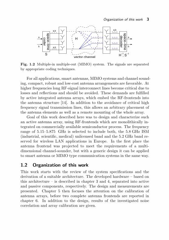
In the late 1990s an entirely different approach was proposed: fromthe standpoint of information theory, a system with multiple transmitand receive antennas provides a higher theoretical capacity to exchangedata, regardless of the geometrical arrangement. This capacity can beexploited by applying suitable space-time coding schemes [9, 10]. A sys-tem block diagram is shown in Fig. 1.2. The wave propagations are nowseen as a multi-dimensional vector channel. It was found that multi-pathpropagation improves the statistical properties of this channel and, there-fore, turns into an advantage. Channel measurements in realistic scenar-ios [11,12] confirm the potential of these so-called multiple-input multiple-output (MIMO) systems. This new field has triggered a lot of researchinterest all over the world. It can be anticipated that the commercialapplication of this new technique will first enhance wireless LANs, wherehigher data rates are already requested nowadays.
To find the optimum system design it is mandatory, among other is-sues, to understand the characteristics of multi-dimensional transmissionchannels. These can be studied using a suitable channel sounder [13].
Organization of this work 3
H
decoder
space−
time
space−
time
coder
vector channel
b b
a,b
a,b
a a
a,b
S −1, SH
−1
Fig. 1.2 Multiple-in multiple-out (MIMO) system. The signals are separated
by appropriate coding techniques.
For all applications, smart antennas, MIMO systems and channel sound-ing, compact, robust and low-cost antenna arrangements are favorable. Athigher frequencies long RF-signal interconnect lines become critical due tolosses and reflections and should be avoided. These demands are fulfilledby active integrated antenna arrays, which embed the RF-frontends intothe antenna structure [14]. In addition to the avoidance of critical highfrequency signal transmission lines, this allows an arbitrary placement ofthe antenna elements as well as a remote mounting of the whole array.
Goal of this work described here was to design and characterize suchan active antenna array, using RF-frontends which are monolithically in-tegrated on commercially available semiconductor process. The frequencyrange of 5.15–5.875 GHz is selected to include both, the 5.8 GHz ISM(industrial, scientific, medical) unlicensed band and the 5.2 GHz band re-served for wireless LAN applications in Europe. In the first place theantenna frontend was projected to meet the requirements of a multi-dimensional channel-sounder, but with a generic design it can be appliedto smart antenna or MIMO type communication systems in the same way.
1.2 Organization of this work
This work starts with the review of the system specifications and thederivation of a suitable architecture. The developed hardware – based onthis architecture – is described in chapter 3 and 4, separated into activeand passive components, respectively. The design and measurements arepresented. Chapter 5 then focuses the attention on the calibration ofantenna arrays, before two complete antenna frontends are reported inchapter 6. In addition to the design, results of the investigated noisecorrelation and array calibration are given.


2
System design
This chapter describes the design considerations which lead to the finalsystem architecture and to the specifications of the individual buildingblocks. The standard single channel case is discussed before it is focusedon the aspects associated with a multiple antenna system. These includethe antenna placement as well as the distribution of the local oscillatorsignal. The latter leads to a discussion of the noise effects in multiple an-tenna systems, where in particular the correlation between the individualchannels plays an important role. Last, a smart antenna test-bed is de-scribed, which utilizes the realized antenna frontend and which is helpfulto characterize the developed hardware on a system level, as it will beseen later.
2.1 Receiver design
2.1.1 Dynamic range
Fig. 2.1 shows a possible power density spectrum as it could be observed atthe input of a wireless mobile communication system. It illustrates one ofthe basic challenges in radio receiver design: the power of the informationcarrying signal varies over a broad range. Dependent on the distancebetween transmitter and receiver it can be close to the noise floor, or highenough to saturate the sensitive input stages. Furthermore, other signalsfrom other communication systems, radars, microwave ovens or unwantedradiation from electrical devices might be present. Often the power ofthese interfering signals surmount the power of the weak signal-of-interestby orders of magnitude. It is therefore mandatory, that a wireless receiverexhibits a high dynamic range to avoid nonlinear effects caused by strongsignals, while keeping it sensitive on the other hand.
Generally, nonlinearities lead to two unwanted effects: first, a strongsignal exhibiting a certain level drives the circuit into compression. Thisleads to a decrease of gain, not only for this strong signal, but also for othersignals received. This phenomenon is known as blocking. Second, even

6 System design
0 5 10 15−180
−160
−140
−120
−100
−80
−60
−40
−20
0
20
freq [GHz]
pow
er [d
Bm
]signal of
interest
Fig. 2.1 Example of a received power density spectrum (solid) and blocking
mask of HIPERLAN/2 [15] (dashed line).
small nonlinearities give rise to intermodulation products. These productsappear at all sum- and difference- frequencies fIM = ±nf1 ± mf2 of twosignals at the frequencies f1, f2 and their m-th and n-th harmonics. Themost critical are the 3rd order products that appear at the frequencies2f1 − f2 and 2f2 − f1. If f1 and f2 are closely spaced, these products arealso located very close and cannot be simply filtered away.
For any practical system, reasonable assumptions have to be madeconcerning the occurring power levels and interferer. Being able to handlethese specified cases, the system should master most of all relevant prac-tical situations. Therefore, wireless standards typically define a blockingmask. To be compliant with the standard the receiver needs to tolerateany signal within this mask and still receive the signal-of-interest. Forthe present system, the blocking mask defined by the European HIPER-LAN/2 wireless LAN standard [15] is used as a reference. This mask isalso shown in Fig. 2.1.
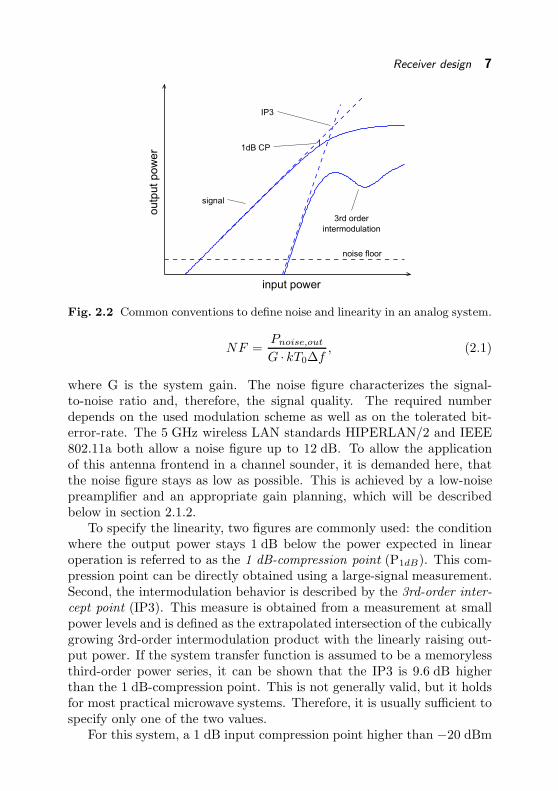
For the circuit design it is helpful to use some easy-to-determine uni-versal figures, which describe noise and linearity behavior of the functionalblocks. Fig. 2.2 illustrates the common conventions.
At the output a certain noise floor is present, which consists of the am-plified thermal noise (Pnoise = kT0∆f) and a contribution of the receivercircuit, described by the noise figure (NF)
Receiver design 7
Fig. 2.2 Common conventions to define noise and linearity in an analog system.
NF =Pnoise,out
G · kT0∆f, (2.1)
where G is the system gain. The noise figure characterizes the signal-to-noise ratio and, therefore, the signal quality. The required numberdepends on the used modulation scheme as well as on the tolerated bit-error-rate. The 5 GHz wireless LAN standards HIPERLAN/2 and IEEE802.11a both allow a noise figure up to 12 dB. To allow the applicationof this antenna frontend in a channel sounder, it is demanded here, thatthe noise figure stays as low as possible. This is achieved by a low-noisepreamplifier and an appropriate gain planning, which will be describedbelow in section 2.1.2.
To specify the linearity, two figures are commonly used: the conditionwhere the output power stays 1 dB below the power expected in linearoperation is referred to as the 1 dB-compression point (P1dB). This com-pression point can be directly obtained using a large-signal measurement.Second, the intermodulation behavior is described by the 3rd-order inter-cept point (IP3). This measure is obtained from a measurement at smallpower levels and is defined as the extrapolated intersection of the cubicallygrowing 3rd-order intermodulation product with the linearly raising out-put power. If the system transfer function is assumed to be a memorylessthird-order power series, it can be shown that the IP3 is 9.6 dB higherthan the 1 dB-compression point. This is not generally valid, but it holdsfor most practical microwave systems. Therefore, it is usually sufficient tospecify only one of the two values.
For this system, a 1 dB input compression point higher than −20 dBm

8 System design
Table 2.1 Initial specifications of the individual receivers.
Specification Value
RF frequency 5.125 – 5.875 GHzRF dynamic range -75 – -35 dBmIF bandwidth 250 MHzIF output power -40 – 0 dBmconverter noise figure < 4dBinput 1dB-compression point > -20 dBmlinearity/ IP3 > -10 dBmpower consumption not critical
is demanded. This fulfills the specifications of both wireless LAN stan-dards, HIPERLAN/2 [15] and IEEE 802.11a. In addition to the require-ments of these standards, a high bandwidth at the intermediate frequency(IF) of 250 MHz is needed for the channel sounding application. To givean overview, the RF specifications are summarized in Tab. 2.1.
2.1.2 Receiver architecture
The classical superheterodyne architecture, on the one hand, is a veryflexible concept, which can be adapted to virtually any wireless receiver.On the other hand, it always requires appropriate filters to suppress theoccurring image bands. Sharp transitions between pass- and stop-bandmight be required as well as a high stop-band attenuation. Both mightbe difficult to realize with monolithically integrated circuits due to in-ternal coupling and high component variations. For integrated receivers,therefore, different architectures are preferred:
The direct conversion receiver avoids the image-frequency problem byconverting to an intermediate frequency of zero. As a drawback, it issensitive to self-mixing effects, which appear as a DC component as well.Compared to a conversion to a higher IF, the direct conversion receiversuffers from a stronger 1/f-noise.
These problems are avoided by the low-IF or image reject receiver [16].The received signal is converted down using two orthogonal LO signalsof 0 and 90 phase difference. This yields a quadrature and in-phasecomponent. This complex signal contains the image and wanted bandas negative and positive frequencies, respectively. The complex filteringcan be carried out in the analog or the digital domain, alternatively. Theimage-reject architecture is sensitive to amplitude and phase mismatchesin the quadrature signals. This becomes critical if a wide bandwidth isneeded.

Receiver design 9
RF frontend
LO1
LO2
Fig. 2.3 Simplified scheme of the super-heterodyne receiver concept. The RF
front-end is the main focus of this work.
For the current design, a high flexibility and a modular system iswanted. Therefore, the classical superheterodyne architecture is favored.To relax the specifications on the necessary filters, a sufficiently high firstIF of 1.45 GHz is chosen. A LO frequency above the signal frequency(fLO = fRF + fIF ) is selected for two reasons: the local oscillators needless relative tuning range for the same RF-bandwidth and the image bandmoves to a “quiet” band, reducing the attenuation the image filter needs toprovide. The first conversion step is followed by a second downconversionto a 150 MHz. Fig. 2.3 shows the simplified block diagram of the com-plete analog processing chain. This work only focusses on the indicatedRF-frontend.
The frontend itself starts with a coarse frequency pre-selection to re-duce the blocking capability by out-of-band signals. Here, this task isinherently performed by the frequency-selective behavior of the antennaand the subsequent amplifier. This first amplifier is optimized for lownoise, as it determines the main contribution to the system noise-figure.
The bottleneck which limits the dynamic range is typically representedby the mixer. A resistive mixer is selected here, as passive mixer show asignificantly higher linearity. Another advantage for this particular systemcan be explained looking at Fig. 2.4, where the typical conversion char-acteristics of both types are shown: the active mixer typically achieves aconversion gain while requiring less LO power. At rising LO power thegain drops quickly, resulting in a small range of operation. The resistivemixer shows a constant performance over a broader interval of LO pow-ers. This is advantageous in a multiple channel system, where the LOneeds to be distributed and no identical powers can be guaranteed. Themissing conversion gain and higher LO power requirements can easily becompensated by additional amplifiers.
Starting from a given input compression point P1dB ≈ +5 . . .+10dBmand conversion loss g ≈ −8 . . . − 6dB of the mixer, a gain of 20 to 25 dBis needed from the low-noise amplifier and filter section. This avoids a

10 System design
conv
ersi
on g
ain
[dB
]LO power
passive FET mixer
active Gilbert mixer
Fig. 2.4 Typical conversion characteristics of passive FET mixer (solid line)
and active Gilbert mixer (dashed line). The active mixer provides conversion
gain at lower LO power, but the range of operation is limited.
compression of the mixer, while the signal level at the output of the mixerremains sufficiently high above the noise floor to keep its influence on thesystem noise figure negligible. Approximately 20 dB of gain need to beprovided by the IF amplifier to reach the required output power-level.
RF and IF amplifiers both have to show high linearity, as the receivedsignals generally can show a non-constant envelope modulation. If powerconsumption is critical, the LO amplifier can be a nonlinear amplifier toreach a higher efficiency. It has to be considered that a nonlinear amplifiercould upconvert 1/f -noise, leading to additional uncorrelated phase noisein a multiple antenna system (see also section 2.3).
2.2 Multiple antenna system
2.2.1 Noise and linearity
Moving from the single-channel receiver to a multi-channel system, thereare two general differences: the signal power is shared by all elementsand the increased effective antenna area provides additional antenna gain.This has different implications for the transmit and the receive case.
In an N-element transmit array only the n-th fraction of the overalloutput power needs to be delivered by a single element. Smaller poweramplifiers can be chosen, which are easier to fabricate, cheaper and haveless power dissipation. If the signal-to-noise ratio is kept constant, or theeffective isotropic radiated power (EIRP) is limited by legal regulations,the individual output power even has to be reduced by 1/N2 to compensatefor the array gain.
In the receive case, the distribution of the signal energy cannot di-rectly be turned into an advantage: unless the transmit power is lowered,
Multiple antenna system 11
AD
AD
sp
ace
−tim
e
pro
ce
sso
r
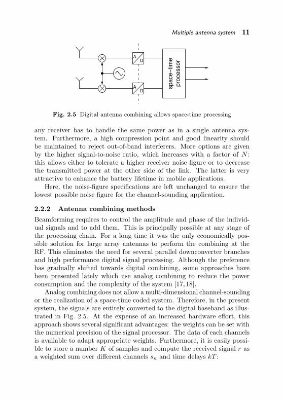
Fig. 2.5 Digital antenna combining allows space-time processing
any receiver has to handle the same power as in a single antenna sys-tem. Furthermore, a high compression point and good linearity shouldbe maintained to reject out-of-band interferers. More options are givenby the higher signal-to-noise ratio, which increases with a factor of N :this allows either to tolerate a higher receiver noise figure or to decreasethe transmitted power at the other side of the link. The latter is veryattractive to enhance the battery lifetime in mobile applications.
Here, the noise-figure specifications are left unchanged to ensure thelowest possible noise figure for the channel-sounding application.
2.2.2 Antenna combining methods
Beamforming requires to control the amplitude and phase of the individ-ual signals and to add them. This is principally possible at any stage ofthe processing chain. For a long time it was the only economically pos-sible solution for large array antennas to perform the combining at theRF. This eliminates the need for several parallel downconverter branchesand high performance digital signal processing. Although the preferencehas gradually shifted towards digital combining, some approaches havebeen presented lately which use analog combining to reduce the powerconsumption and the complexity of the system [17,18].
Analog combining does not allow a multi-dimensional channel-soundingor the realization of a space-time coded system. Therefore, in the presentsystem, the signals are entirely converted to the digital baseband as illus-trated in Fig. 2.5. At the expense of an increased hardware effort, thisapproach shows several significant advantages: the weights can be set withthe numerical precision of the signal processor. The data of each channelsis available to adapt appropriate weights. Furthermore, it is easily possi-ble to store a number K of samples and compute the received signal r asa weighted sum over different channels sn and time delays kT :

12 System design
r(t + K ·T ) =
N∑
n=1
K∑
k=1
wn,k · sn(t − kT ), (2.2)
with T being the time between to samples and wn,k the complex weightfor channel n and delay kT . This corresponds to a varying directionalpattern for each time delay. In a typical mobile wireless scenario, differentpaths of propagation are observed; each with a certain angle of incidentand delay. Using space-time processing, different signals can be separatedmore precisely than with a static directional pattern achieved with analogantenna combining.
Several attempts have been exercised to reduce the hardware necessaryfor array processing. They include time-domain [19] or frequency-domain[20] multiplexing prior to converting the signal to baseband. However, itis found that the lower component count is paid for by higher bandwidthrequirements or a large number of frequency synthesizers, respectively.
2.2.3 Local oscillator distribution
For all architectural choices except RF combining, a local oscillator signalhas to be provided at all receiver branches. As shown in Fig. 2.6, this canbe done by either using a splitting network, or by generating the signallocally at each antenna element. In the latter case it is mandatory toestablish a fixed phase relationship between all LO signals. This can bedone by deriving the local signal from a reference, either by using frequencymultiplication, injection locking or a phase-locked loop.
The constant phase relationship has to be maintained for every neededLO signal, including the clock frequency of the analog-digital converter.In this work, the distribution of the high frequency LO signal was selectedto guarantee the best LO phase correlation possible. The effect of non-constant phases is discussed in section 2.3.4.
referencephase
individual LO common LO
Fig. 2.6 LO distribution: central or local LO
Multiple antenna system 13
2.2.4 Antenna placement
Smart antennas
Most of the known smart antenna techniques base on Huygens principleof elementary sources and quasi-optical wave propagation. This impliesthat, if a coherent signal is emitted from several positions ~xn, this leadsto constructive and destructive interference patterns.
With the propagation constant k = 2πλ the phase shift at the location
~y is given by∆φ = −k| ~xn − ~y|. (2.3)
If each source has its own amplitude and phase, expressed in the complex“weights” wn and gn (φ, θ) is the individual element pattern, the superim-
posed signal at point ~d can be calculated as
g(~y) =N∑
n=0
wn · gn (φ, θ) · exp(−ik| ~xn − ~y|), (2.4)
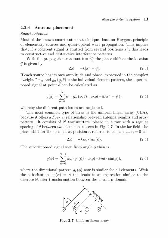
whereby the different path losses are neglected.The most common type of array is the uniform linear array (ULA),
because it offers a Fourier relationship between antenna weights and arraypattern. It consists of N transmitters, placed in a row with a regularspacing of d between two elements, as seen in Fig. 2.7. In the far-field, thephase shift for the element at position n referred to element at n = 0 is
∆φ = −knd · sin(φ). (2.5)
The superimposed signal seen from angle φ then is
g(φ) =
N−1∑
n=0
wn · gi (φ) · exp(−knd · sin(φ)), (2.6)
where the directional pattern gi (φ) now is similar for all elements. Withthe substitution sin(φ) = u this leads to an expression similar to thediscrete Fourier transformation between the u- and n-domain:
∆lφ
wave front
d
Fig. 2.7 Uniform linear array

14 System design
g(u) = gi (u) ·
N−1∑
n=0
w(n) · exp(−kd ·n ·u) (2.7)
As a consequence of this, all relationships known from signal processingin the time and frequency domain can be applied on this transformationbetween spatial and angular domain. Similar to the Nyquist rate, anantenna spacing of d ≤ λ0/2 is needed to represent the entire angularrange −1 ≤ u ≤ 1. Otherwise replica of the array pattern appear, whichcan not be controlled independently.
For this particular antenna array it has to be considered that it doesnot have a fixed frequency, but a possible range of 5.15 to 5.875 GHz.Strictly it would be reasonable to choose an antenna spacing of λ0/2 ac-cording to the highest occurring frequency. Here, the element spacing isapproximately selected for the center of the band at 5.5 GHz, resulting ina center-to-center distance of 27.3 mm. For higher frequencies this causesreplica to appear. These replica appear outside of the beam width of theantenna elements and can be tolerated.
So far it was assumed that all antennas operate independently fromeach other. In the realistic case of mutually coupled antennas, this slightlyincreased distance helps to lower the antenna coupling. The antenna cou-pling will be discussed more detailed later in chapter 4.3.
MIMO systems
If the frontend is intended to serve as a part of a MIMO-system, the angleof view has to be changed entirely. It is one reason for the high attrac-tiveness of MIMO-systems that the geometrical antenna arrangement issimply included into the unknown channel response. On the one hand thisallows almost all arbitrary antenna placements, as long as a data trans-mission is possible between transmitter and receiver. On the other hand,this makes it more difficult to determine the best configuration.
A given antenna setup in its environment can be evaluated as follows:the system of M transmit and N receive antennas can be seen as a vectorchannel HM×N . Without considering the concrete coding techniques, anupper limit for the instantaneous channel capacity of a stochastic MIMOchannel can be given from theoretical considerations [9]:
C = log2 det
(I +
ρ
NtHHT
), (2.8)
where ρ is the average SNR at each receiver, Nt the number of trans-mit antennas and I is the identity matrix. The objectives of antenna
Multiple antenna system 15
0 0.5 1 1.5 2 2.5 3−0.5
0
0.5
1
∆x/λ
R(∆
x)
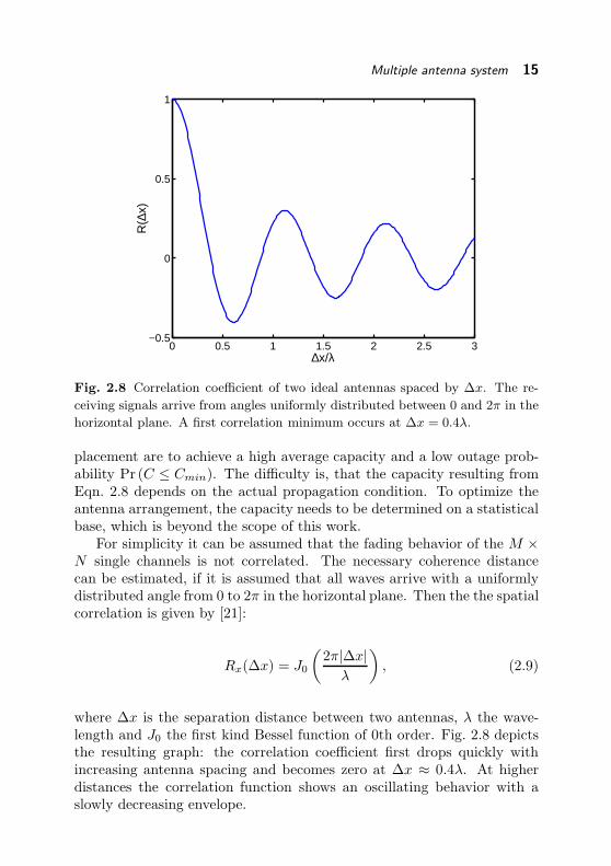
Fig. 2.8 Correlation coefficient of two ideal antennas spaced by ∆x. The re-
ceiving signals arrive from angles uniformly distributed between 0 and 2π in the
horizontal plane. A first correlation minimum occurs at ∆x = 0.4λ.
placement are to achieve a high average capacity and a low outage prob-ability Pr (C ≤ Cmin). The difficulty is, that the capacity resulting fromEqn. 2.8 depends on the actual propagation condition. To optimize theantenna arrangement, the capacity needs to be determined on a statisticalbase, which is beyond the scope of this work.
For simplicity it can be assumed that the fading behavior of the M ×N single channels is not correlated. The necessary coherence distancecan be estimated, if it is assumed that all waves arrive with a uniformlydistributed angle from 0 to 2π in the horizontal plane. Then the the spatialcorrelation is given by [21]:
Rx(∆x) = J0
(2π|∆x|
λ
), (2.9)
where ∆x is the separation distance between two antennas, λ the wave-length and J0 the first kind Bessel function of 0th order. Fig. 2.8 depictsthe resulting graph: the correlation coefficient first drops quickly withincreasing antenna spacing and becomes zero at ∆x ≈ 0.4λ. At higherdistances the correlation function shows an oscillating behavior with aslowly decreasing envelope.

16 System design
It can be concluded that a linear array with a spacing of λ0/2 at5.5 GHz does not represent the best solution, but to maintain the com-patibility with beamforming applications it is a good compromise.
It has to be remarked that this simplified approach assumes an en-vironment with rich scattering. For a set of antennas mounted with nolocal scatterers near, like e.g. a base station on a mast top, the coherencedistance can be several tens of wavelengths.
Also it is interesting to investigate different antenna orientations. Itwas demonstrated that a compact antenna arrangement can be foundwhich makes use of polarization and pattern diversity, improving the per-formance at the same time [22].
2.3 Noise in multiple antenna systems
2.3.1 Signal and noise model
One of the main advantages of multiple antenna systems is their ability toincrease the signal-to-noise ratio in a given situation. Any beamformingoperation bases on the addition of the N received signals sn to
r(t) =
N∑
n=1
(sn(t) + nn(t)
), (2.10)
where nn describes the additional noise at each receiver. Assuming thesignals sn originate from the same source, correlated and perfectly in phase(by adequate pre-processing), the signal amplitudes add1
|rsignal(t)|2 =
∣∣∣∣∣
N∑
n=1
sn(t)
∣∣∣∣∣
2
, (2.11)
while the noise contributions are uncorrelated (Eni ·nj = 0 and E. . .is denoting the expectation value) sum up in terms of power
|rnoise(t)|2 =
N∑
n=1
|nn(t)|2. (2.12)
If noise and signal powers are equal for all elements E|nn|2 = n2
0 andE|sn|
2 = s20 respectively, the signal-to-noise ratio is proportional to the
number of elements
1This expression violates the law of conservation of energy, indicating that Eqn. 2.10cannot be realized using passive components. This affects the calculation of the overallgain. However, the calculation of the signal-to-noise ratio is not affected.

Noise in multiple antenna systems 17
nois
e w
avescoupling
mutual
c2
c1
G
Fig. 2.9 Generation of correlated noise by mutual coupling
SNR = N ·s0
n0. (2.13)
This demonstrates that the basic property that makes the difference be-tween signal and noise is the correlation between the channels. Thereforeit is important to identify and control all effects that lead to correlatednoise and decorrelation of signals, respectively.
2.3.2 Noise correlation
Several mechanisms are known, that lead to correlated noise:
• If noise is received, which is radiated from a single source, e.g. abody with a significantly higher temperature than the receiver, oranother device. This kind of correlated noise principally can not bedistinguished from a signal and has to be treated as interferer.
• The pre-amplifiers at the input produce noise. The main portion ofthis noise is found at the output, where it is amplified together withthe signal. A fraction of the amplifiers noise is also found at the input.Through mutual antenna coupling it reaches the neighbor elementwhere it gets amplified causing correlated noise [23], as sketched inFig. 2.9. The noise coupling ratio is defined as Gc1Γi
c2, where G is
the amplifier gain, c1 and c2 the forward and backward travellingnoise waves and Γi the active reflection coefficient of the array. Forapplications in communication systems one aims to realize low mutualantenna coupling. If it is assumed that the output noise c2 is exceedsthe noise wave at the input by the amplifier gain Gc1 ≈ c2, thecoupling coefficient is in the order of the s-parameter S21 measuredbetween to antennas in the passive array. Typically this is −15 dB orlower.
• The system itself radiates signals or interaction occurs over the com-mon power supply. Notably the digital part with its fast transientsand strong clock signal is known to emit unwanted energy. This powercouples to the analog part and appears as spurious responses afteranalog/ digital conversion. Theoretically it is possible to completelysuppress it, but in practical applications a certain amount of coupling

18 System design
f0
pow
er d
ensi
ty
frequency
φ
j · a ·φ
a
⇐⇒
Fig. 2.10 Phase noise equivalence in frequency and time domain
has to be tolerated. Although the resulting spurious responses onlyaccount for a small fraction of the overall noise power, it was observedthat they can be highly correlated [24]. The influence of this effect isdifficult to predict, as it is based on parasitic effects.
2.3.3 Phase noise
Phase noise is a phenomenon associated with frequency sources. Noisesources affect the frequency generation process which leads to small de-viations from the ideal sinusoidal waveform. The output of a frequencysource showing phase noise can be written as
sLO(t) = s0 · cos(2πf0t + φ(t)
), (2.14)
where φ(t) is the temporal phase deviation from the ideal signal. In thefrequency domain this leads to a broadening of what should be a singleline at the frequency of oscillation. A common method of characterizingthe phase noise of frequency sources is to give the spectral density (usuallyreferred to 1 Hz bandwidth) at a certain spacing ∆f away from the carrier.Its power density is expressed relatively to the carrier using the logarithmicmeasure dBc/Hz.
For small phase deviations a simple relationship between frequencydomain characterization and time domain phase jitter can be derived asillustrated in Fig. 2.10. Under the assumption that |φ| π
2 , the com-plex bandpass representation (omitting exp(j2πf0t)) can be linearized asfollows:
a · exp (φ(t)) ≈ a + j · a ·φ(t) (2.15)
The power a2 corresponds to the carrier power. Therefore, the powercontained in the noise sidebands must be the orthogonal perturbation.For a given bandwidth B the mean phase deviation |φ|2 is [25]
|φ|2 ≈
∫ B
0
Pnoise(f)
Pcarrierdf. (2.16)
Noise in multiple antenna systems 19
I
Q
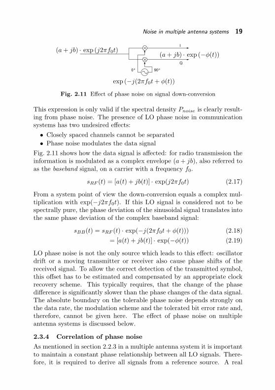
90°0°
(a + jb) · exp (j2πf0t)
exp (−j(2πf0t + φ(t))
(a + jb) · exp (−φ(t))
Fig. 2.11 Effect of phase noise on signal down-conversion
This expression is only valid if the spectral density Pnoise is clearly result-ing from phase noise. The presence of LO phase noise in communicationsystems has two undesired effects:
• Closely spaced channels cannot be separated
• Phase noise modulates the data signal
Fig. 2.11 shows how the data signal is affected: for radio transmission theinformation is modulated as a complex envelope (a + jb), also referred toas the baseband signal, on a carrier with a frequency f0.
sRF (t) = [a(t) + jb(t)] · exp(j2πf0t) (2.17)
From a system point of view the down-conversion equals a complex mul-tiplication with exp(−j2πf0t). If this LO signal is considered not to bespectrally pure, the phase deviation of the sinusoidal signal translates intothe same phase deviation of the complex baseband signal:
sBB(t) = sRF (t) · exp(−j(2πf0t + φ(t))) (2.18)
= [a(t) + jb(t)] · exp(−φ(t)) (2.19)
LO phase noise is not the only source which leads to this effect: oscillatordrift or a moving transmitter or receiver also cause phase shifts of thereceived signal. To allow the correct detection of the transmitted symbol,this offset has to be estimated and compensated by an appropriate clockrecovery scheme. This typically requires, that the change of the phasedifference is significantly slower than the phase changes of the data signal.The absolute boundary on the tolerable phase noise depends strongly onthe data rate, the modulation scheme and the tolerated bit error rate and,therefore, cannot be given here. The effect of phase noise on multipleantenna systems is discussed below.
2.3.4 Correlation of phase noise
As mentioned in section 2.2.3 in a multiple antenna system it is importantto maintain a constant phase relationship between all LO signals. There-fore, it is required to derive all signals from a reference source. A real

20 System design
LO signal with phase noise has a small bandwidth and is coherent over acertain time. The differences of line lengths which occur in a typical LOdistribution network in an array system are in the range of wavelengths.This is not sufficient to cause any decorrelated LO phases at the individ-ual receivers. Nevertheless, there are possible sources of additional phasenoise:
• A phase-locked loop (PLL) is an attractive method to lock a localhigh-frequency oscillator on a reference signal. Within the loop band-width the oscillator phase noise is suppressed, its phase follows thereference. The phase noise outside the loop bandwidth adds as un-correlated fraction to the reference phase noise. If the phase detectorand loop filter are not noiseless, their noise also contributes to theuncorrelated phase noise.
• All non-linear circuits like frequency doubler, tripler or amplifierswith high efficiency principally show mixing effects. This leads to anup-conversion of 1/f -noise, usually present in semiconductor devices.It appears as additional phase noise.
If the LO signal at the nth branch contains partly correlated phasenoise, the phase deviation φn(t) can be split into a fully correlated meanphase deviation φ(t) common for all channels and an independent relativeangle φ′
n(t):φn(t) = φ(t) + φ′
n(t) (2.20)
Omitting the amplitude noise, Eqn. 2.10 becomes
r(t) =
N∑
n=1
sn(t) · exp(−j(φ(t) + φ′
n(t))), (2.21)
where the correlated phase noise can be moved out of the sum:
r(t) = exp(−jφ(t)
) N∑
n=1
sn(t) · exp (−jφ′n(t)) (2.22)
This demonstrates that the correlated portion of phase noise φ(t) affectsthe output signal, where it has to be estimated and compensated togetherwith possible frequency offsets and Doppler-shifts. The uncorrelated frac-tion φ′
n(t) disturbs the signal combining process itself, leading to a degra-dation in the array interference cancellation ability [25].
The effect of additional phase noise generated by LO-amplifiers or mix-ers generally is difficult to measure. The phase noise of low-noise signalgenerators, needed for the measurement, typically exceeds this contribu-tion and covers the effect.

Testbed architecture 21
At the time of the design, no publications of experimental results re-garding the phase noise correlation were available. It could be demon-strated that a slight phase decorrelation occurs, however at a level lowenough for most practical applications. For details see chapter 6.3.
In multi-antenna channel-sounding systems the individual paths areoften measured sequentially by switching between the antenna elements.In this case the absolute phase-noise value has to be low to ensure theright estimate of the channel capacity [26].
2.3.5 System noise model
In a complex system like in Fig. 2.13 several sources of both, phase noiseand amplitude noise, are present. Phase noise is introduced at every down-conversion step, including the analog to digital conversion. The additivenoise added by each stage is down-converted together with the signal, thusaffected by phase noise as well. This additive noise can be assumed not tobe correlated with the phase noise. Therefore, the complex noise-vectorn = nI + j ·nQ becomes
n′ = (nI + j ·nQ) exp(−jφ) (2.23)
without changing its statistical properties.For the practical case that phase noise contributions are sufficiently
correlated, all correlated additive noise sources can be combined in a noisevector ncorr which gives a different noise behavior at the output, depen-dent on the actual beam-forming. The power of all uncorrelated noisesources nuncorr adds to the system output, independent of the beam-forming operation.
The uncorrelated and correlated phase noise powers sum up to a singlephase shift φn for each branch and one common phase shift φ at the output,respectively. This leads to the system noise model shown in Fig. 2.12.
2.4 Testbed architecture
Fig. 2.13 shows the architecture of the entire “SANTRES” testbed. Theclassical super-heterodyne architecture with two analog conversion stepsto 1.45 GHz and 150 MHz is used, as described above. The signal is band-pass filtered and sub-sampled at a rate of 52 MHz. The digital signalthen is further processed and decimated by a programmable factor [27].Subsequently, the signal is either processed or stored.
The whole receiver chain from RF to baseband is carried out four timesin parallel. The local oscillator signals are generated using programmablesynthesizers. To obtain the best possible phase correlation, these signalsare divided and equally distributed to all branches.

22 System design
The first down-converter stages, which are the most critical and sensi-tive parts of the system, are directly integrated together with the antennaarray. This reduces the influence of phase instabilities of cables and con-nectors, allowing also remote mounting of the active array.
To calibrate the phase and amplitude inequalities of the receiver branchesit is possible to apply a calibration signal (not shown in the diagram). Thecalibration aspects are discussed in chapter 5.
spatial processing
r
ncorr
φ
nuncorr
1φ
2φ
3φ
4φ
s3
s2
s1
s4
Fig. 2.12 System noise model, reduced to a minimum of correlated and uncor-
related additive and phase-noise sources.
AD
LO 1
clock
and
deci
mat
ion
I,Q
proc
essi
ngan
d st
orag
e
LO 2
activ
e an
tenn
a ar
ray
digi
tal d
ownc
onve
rter
sample
Fig. 2.13 Simplified block diagram of “SANTRES” system, generation and
distribution of the calibration signal is not shown here.

3
Integrated circuit design
In this chapter the design and characterization of monolithically integratedcircuits is described, which base on the system level considerations in theprevious chapter. The available technologies are reviewed and the choiceis motivated. Starting from the concepts of the different key components,the whole RF frontend can be integrated on a single chip. In particularthis includes also the image filter, which is realized as a lumped-elementpassive on-chip filter.
In addition to these circuits required for the proposed frontend, fur-ther circuits are reported: a power amplifier is described which is usedto investigate the calibration of transmit arrays (see chapter 5.4). To ex-ploit the abilities for future high-frequency low-cost applications, a 11 GHzdownconverter is demonstrated on a 47 GHz-ft SiGe process.
3.1 Process technology
3.1.1 Choice of technology
Today, a large number of various technologies are available, each with itsown advantages and applications. High-frequency analog applications tra-ditionally employ III/V-technologies based on GaAs or InP, which benefitfrom a high electron mobility and offer transit frequencies beyond 500 GHz(InP PHEMT [28]).
The enormous success of personal computers, on the other hand, leadto a rapid development of silicon-based technologies, CMOS in particu-lar. The available complementary device allows simple logical gates andtherefore a very high integration of digital logic. Silicon shows excellentmechanical and thermal properties at low material costs. This combina-tion of very high integration with easy handling of large wafers resultsin low costs for high-volume production, and explains why strong effortswere made to improve this technology.
The trend of steadily increasing processor speeds caused an aggres-sive down-scaling of the transistor devices below 100 nm gate-length. The
24 Integrated circuit design
Isolation ImplantN+N+
Metal 0
Metal 1 -2um
Metal 2
Dielectric
Dielectric
Metal 2 -4um
Dielectric
MIM Metal
E,D,G MESFET NiCr RMIM Capacitor
Semi-Insulating GaAs Substrate
Isolation ImplantN+N+
Metal 0
Metal 1 -2um
Metal 2
Dielectric
Dielectric
Metal 2 -4um
Dielectric
Isolation ImplantN+N+
N-/P-Channel
N+ N+
Metal 0
Metal 1 Metal 1 Metal 1 -2um
Metal 2
Dielectric
Dielectric
Metal 2 -4um
Dielectric
MIM Metal NiCr
E,D,G MESFET NiCr ResistorMIM Capacitor
Semi-Insulating GaAs Substrate
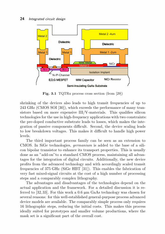
Fig. 3.1 TQTRx process cross section (from [29])
shrinking of the devices also leads to high transit frequencies of up to243 GHz (CMOS SOI [30]), which exceeds the performance of many tran-sistors based on more expensive III/V-materials. This qualifies silicontechnologies for the use in high-frequency applications with two constraints:the pre-doped conductive substrate leads to losses, which makes the inte-gration of passive components difficult. Second, the device scaling leadsto low breakdown voltages. This makes it difficult to handle high powerlevels.
The third important process family can be seen as an extension toCMOS. In SiGe technologies, germanium is added to the base of a sili-con bipolar transistor to enhance its transport properties. This is usuallydone as an ”add-on”to a standard CMOS process, maintaining all advan-tages for the integration of digital circuits. Additionally, the new deviceprofits from the advanced technology and with accordingly scaled transitfrequencies of 375 GHz (SiGe HBT [31]). This enables the fabrication ofvery fast mixed-signal circuits at the cost of a high number of processingsteps and a comparably complex lithography.
The advantages and disadvantages of the technologies depend on theactual application and the framework. For a detailed discussion it is re-ferred to [32,33]. For this work a 0.6 µm GaAs technology was chosen forseveral reasons: for this well-established general-purpose process advanceddevice models are available. The comparably simple process only requires16 lithographic steps, reducing the initial costs. This makes this processideally suited for prototypes and smaller volume productions, where themask set is a significant part of the overall cost.
Process technology 25
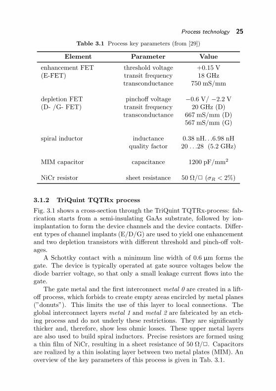
Table 3.1 Process key parameters (from [29])
Element Parameter Value
enhancement FET threshold voltage +0.15 V(E-FET) transit frequency 18 GHz
transconductance 750 mS/mm
depletion FET pinchoff voltage −0.6 V/ −2.2 V(D- /G- FET) transit frequency 20 GHz (D)
transconductance 667 mS/mm (D)567 mS/mm (G)
spiral inductor inductance 0.38 nH. . .6.98 nHquality factor 20 . . .28 (5.2 GHz)
MIM capacitor capacitance 1200 pF/mm2
NiCr resistor sheet resistance 50 Ω/2 (σR < 2%)
3.1.2 TriQuint TQTRx process
Fig. 3.1 shows a cross-section through the TriQuint TQTRx-process: fab-rication starts from a semi-insulating GaAs substrate, followed by ion-implantation to form the device channels and the device contacts. Differ-ent types of channel implants (E/D/G) are used to yield one enhancementand two depletion transistors with different threshold and pinch-off volt-ages.
A Schottky contact with a minimum line width of 0.6 µm forms thegate. The device is typically operated at gate source voltages below thediode barrier voltage, so that only a small leakage current flows into thegate.
The gate metal and the first interconnect metal 0 are created in a lift-off process, which forbids to create empty areas encircled by metal planes(”donuts”). This limits the use of this layer to local connections. Theglobal interconnect layers metal 1 and metal 2 are fabricated by an etch-ing process and do not underly these restrictions. They are significantlythicker and, therefore, show less ohmic losses. These upper metal layersare also used to build spiral inductors. Precise resistors are formed usinga thin film of NiCr, resulting in a sheet resistance of 50 Ω/2. Capacitorsare realized by a thin isolating layer between two metal plates (MIM). Anoverview of the key parameters of this process is given in Tab. 3.1.

26 Integrated circuit design
(a) (b) (d)(c)
Fig. 3.2 Possible LNA configurations: a) active matching b) inductive current
feedback at source (source degeneration) c) RC-feedback d) cascode
3.2 Low-noise amplifier
In the previous chapter 2 it was specified, that the low-noise amplifiershould have 20 to 25 dB of gain, a bandwidth of 5.15 to 5.875 GHz anda noise figure as low as possible. To minimize the influence of out-of-bandinterferers, it is advantageous to use a frequency selective amplifier. Tomeet these requirements, several individually optimized amplifier stagesare cascaded. The design starts with the search of a suitable circuit topol-ogy for the single stage.
3.2.1 Input matching
In a common-source configuration, the input of any field effect transistortypically shows a capacitive behavior over a broad frequency range, be-fore extrinsic inductances and the gate resistance start to dominate closeto the transit frequency. If the gate is reactively matched to a 50 Ω in-put port, this leads to very narrow-band network. Additionally to highlosses introduced by the low-Q passive components, the matching networkbecomes very sensitive to process variations, which makes this straight-forward matching inappropriate for monolithic integration.
A possible solution would be to use a common gate configuration de-picted in Fig. 3.2a, which can be designed to provide an active inputmatching. This topology is often found in broadband amplifiers, but dueto higher noise and poor linearity it is not the best choice for low-noiseamplifiers.
As a solution to the reactive input impedance, inductive current feed-back at the source (see Fig. 3.2b) is widely used, because it unifies severaladvantages: it stabilizes the device, it linearizes the transfer characteris-tic, and it brings together the optimum impedances for power and noisematching. It can be shown [34] that the idealized field effect transistortransforms the source inductance Ls into a resistance seen at the input:

Low-noise amplifier 27
Zin =1
jωCgs+ jωLs +
gmLs
Cgs︸ ︷︷ ︸resistive
, (3.1)
where gm is the transconductance, CGS the gate-source capacitance ofthe device and ω = 2πf is the angular frequency. If the transistor andthe feedback inductor are assumed to be ideal components, the real partresulting from this transformation is noiseless.
RC-feedback, as seen in Fig. 3.2c, does not require a bulky spiral induc-tor. On one hand, the needed resistor and capacitor require significantlyless area and, therefore, make this type of feedback ideal for integration.On the other hand, the resistor represents an additional source of noise,raising the noise figure of the amplifier. For this reason RC-feedback isavoided in the first stages, where the noise contribution is critical.
The cascode configuration, shown in Fig. 3.2d, is often found in low-noise amplifiers. Originally proposed to enhance the gain bandwidth prod-uct by minimizing the effect of the Miller-capacitance, it is attractive alsofor the use in selective amplifiers, because it shows a high gain and mini-mizes the contribution of the consecutive stages to the overall noise figure.As a drawback, the cascode shows a high output impedance. This makesit impossible to realize a broadband power matching to the next stage.Therefore, a cascode topology cannot be used here.
Determining the optimum value Ls for the inductive source degener-ation, it has to be considered that a good input power matching doesnot necessarily yield the best noise-figure. For the practical implementa-tion on a monolithically integrated circuit, two effects play an importantrole: a strong feedback also decreases the gain of the stage, leading to anincreased contribution of the following stage to the overall noise figure.Second, using monolithically integrated inductors with a limited qualityfactor Q, the inductor becomes a significant source of noise itself andshould be kept as small as possible. This leads to a trade-off betweenamplifier mismatch and noise figure.
For the input stage, whose noise contribution is the most critical, areduced feedback is chosen. The best results are achieved for a real partof around 25 Ω, resulting in an an input return loss between −10 dB and−8 dB. The matching network can be further simplified by scaling thetransistor width. For a device of 150 µm gate width, the reactive inputmatching can be realized with a single inductor. This results in both,a broad matching bandwidth and low losses at the amplifier input and,hence, a reduced noise figure.
28 Integrated circuit design
3.2.2 Device scaling
A constraint for device scaling is set by the power handling capability,which determines the compression and intermodulation behavior of thefinal amplifier. Contrary to power amplifiers, where the maximum poweris limited by current and voltage, the output power is limited by the max-imum possible current through the device. This occurs at the maximumgate-source voltage Vd at the onset of gate diode forward conduction. Therange of operation is given by Vd and the threshold voltage Vth. The ab-solute power level and the corresponding voltage range are linked by theeffective input impedance of the device, which scales with the gate width.It can be roughly estimated that doubling the gate width leads to half ofthe input impedance, twice the input power at compression and, there-fore, to a compression point increased by 3 dB. The same argumentationapplies to the linearity and the 3rd-order intercept point.
It is found that a gate width of 600 µm is sufficient to handle the maxi-mum output power of 5 dBm. Therefore, this transistor size is selected forthe last stage. The precedent stages obviously need to handle less powerand smaller devices can be chosen.
To estimate the influence on the system linearity, the total 3rd-orderintercept point of two cascaded amplifiers can be given as [34]
PIIP3tot=
(1
PIIP31
+G1
PIIP32
)−1
, (3.2)
where PIIP31 and PIIP32 are the individual intercept points and G1 is thegain of the first amplifier. If the stages are simply scaled with their gainPIIP32 = G1 ·PIIP31 , the intercept point decreases by 3 dB for each stagethat is added.
The approximate gain of one stage is 8 to 10 dB, thus three stagesare required to reach the specified gain of 20 to 25 dB. Simply scalingwith the stage gain would result in a gate width of 6 to 17 µm, much lessthan the width of 150 µm that was found above for the best matching.Furthermore, the large impedance changes from stage to stage limit thebandwidth of the interstage matching networks.
At the cost of a higher power consumption, the 150 µm device at theinput is maintained and a gate-width ratio of 2 is chosen to obtain atransition to the 600 µm output stage. In addition to the optimal inputmatching, this practically enhances the bandwidth and lowers the IP3.The sensitivity to blocking by strong out-of-band interferers is significantlyreduced, as these mainly saturate the first amplifier stage.
Low-noise amplifier 29
150µm
E−FET
Vdd1 V Vdd2 dd3
1kΩ
1.0nH
1.0
nH
2.3
nH
1.0
nH
RF
in
Vg1
356fF
5k
Ω
Vg2
1.3
nH
1.3
nH
12.5
pF 2
55fF
1.0
nH
255fF
1.2pF0.6
nH
2.8
5nH
E−FET
300µm
0.6
nH
0.6
nH
3.7
nH
2.0
nH
2x E−FET
300µm
356fF
937fF
5kΩ out
RF
890fF
1kΩ
g3V
Fig. 3.3 Schematic of the three stage low-noise amplifier. Bias generation
networks are not shown.
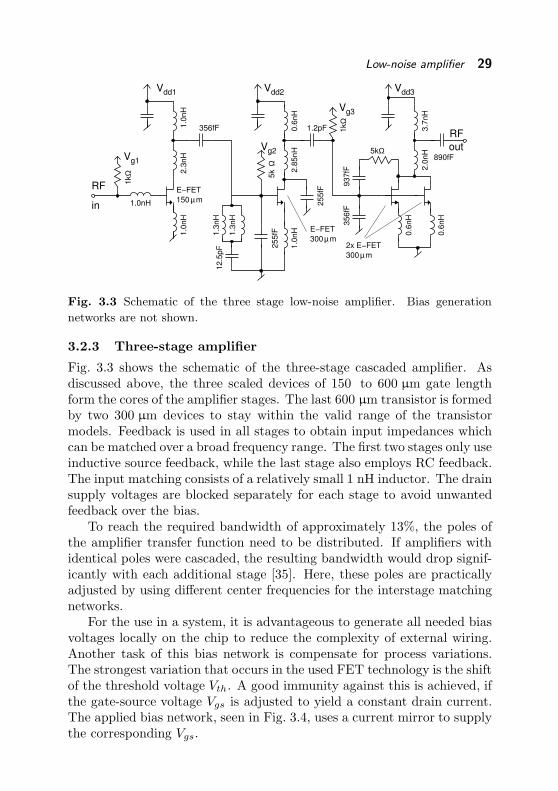
3.2.3 Three-stage amplifier
Fig. 3.3 shows the schematic of the three-stage cascaded amplifier. Asdiscussed above, the three scaled devices of 150 to 600 µm gate lengthform the cores of the amplifier stages. The last 600 µm transistor is formedby two 300 µm devices to stay within the valid range of the transistormodels. Feedback is used in all stages to obtain input impedances whichcan be matched over a broad frequency range. The first two stages only useinductive source feedback, while the last stage also employs RC feedback.The input matching consists of a relatively small 1 nH inductor. The drainsupply voltages are blocked separately for each stage to avoid unwantedfeedback over the bias.
To reach the required bandwidth of approximately 13%, the poles ofthe amplifier transfer function need to be distributed. If amplifiers withidentical poles were cascaded, the resulting bandwidth would drop signif-icantly with each additional stage [35]. Here, these poles are practicallyadjusted by using different center frequencies for the interstage matchingnetworks.
For the use in a system, it is advantageous to generate all needed biasvoltages locally on the chip to reduce the complexity of external wiring.Another task of this bias network is compensate for process variations.The strongest variation that occurs in the used FET technology is the shiftof the threshold voltage Vth. A good immunity against this is achieved, ifthe gate-source voltage Vgs is adjusted to yield a constant drain current.The applied bias network, seen in Fig. 3.4, uses a current mirror to supplythe corresponding Vgs.
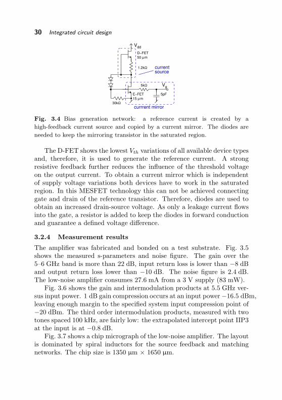
30 Integrated circuit design
Vdd
5pF
D−FET
mµ50
Ω1.2k
Ω30k
15 µm
E−FET
gV5kΩ
currrent mirror
currentsource
Fig. 3.4 Bias generation network: a reference current is created by a
high-feedback current source and copied by a current mirror. The diodes are
needed to keep the mirroring transistor in the saturated region.
The D-FET shows the lowest Vth variations of all available device typesand, therefore, it is used to generate the reference current. A strongresistive feedback further reduces the influence of the threshold voltageon the output current. To obtain a current mirror which is independentof supply voltage variations both devices have to work in the saturatedregion. In this MESFET technology this can not be achieved connectinggate and drain of the reference transistor. Therefore, diodes are used toobtain an increased drain-source voltage. As only a leakage current flowsinto the gate, a resistor is added to keep the diodes in forward conductionand guarantee a defined voltage difference.
3.2.4 Measurement results
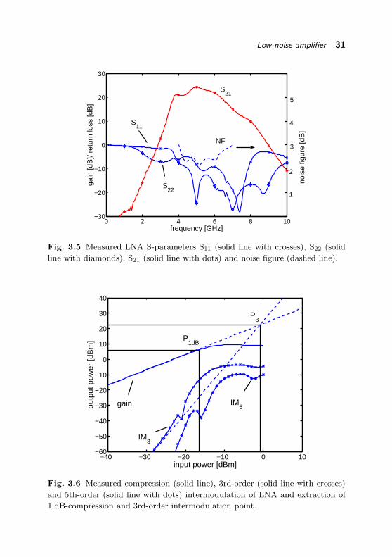
The amplifier was fabricated and bonded on a test substrate. Fig. 3.5shows the measured s-parameters and noise figure. The gain over the5–6 GHz band is more than 22 dB, input return loss is lower than −8 dBand output return loss lower than −10 dB. The noise figure is 2.4 dB.The low-noise amplifier consumes 27.6 mA from a 3 V supply (83 mW).
Fig. 3.6 shows the gain and intermodulation products at 5.5 GHz ver-sus input power. 1 dB gain compression occurs at an input power −16.5 dBm,leaving enough margin to the specified system input compression point of−20 dBm. The third order intermodulation products, measured with twotones spaced 100 kHz, are fairly low: the extrapolated intercept point IIP3at the input is at −0.8 dB.
Fig. 3.7 shows a chip micrograph of the low-noise amplifier. The layoutis dominated by spiral inductors for the source feedback and matchingnetworks. The chip size is 1350 µm × 1650 µm.
Low-noise amplifier 31
0 2 4 6 8 10−30
−20
−10
0
10
20
30
frequency [GHz]
gain
[dB
]/ re
turn
loss
[dB
]S
21
S22
S11
1
2
3
4
5
nois
e fig
ure
[dB
]
NF
Fig. 3.5 Measured LNA S-parameters S11 (solid line with crosses), S22 (solid
line with diamonds), S21 (solid line with dots) and noise figure (dashed line).
−40 −30 −20 −10 0 10−60
−50
−40
−30
−20
−10
0
10
20
30
40
input power [dBm]
outp
ut p
ower
[dB
m] P
1dB
IP3
gain
IM3
IM5
Fig. 3.6 Measured compression (solid line), 3rd-order (solid line with crosses)
and 5th-order (solid line with dots) intermodulation of LNA and extraction of
1 dB-compression and 3rd-order intermodulation point.

32 Integrated circuit design
100 um
bias bias bias
E 150
E 300 2x E300
Fig. 3.7 Micrograph of three stage low-noise amplifier. Chip size is
1350 µm×1650 µm (2.2 mm2).
3.3 Downconverter
In chapter 2 it was stated that a passive resistive mixer is needed to achievea higher dynamic range. It was assumed that this mixer shows a conver-sion loss of 6 to 8 dB, estimated from experience. The LO power is notspecified. For the design of the downconverter it is reasonable to demandthe best achievable performance, rather then aiming for a certain conver-sion loss and LO power. Instead, it is more important to consider thelinearity requirements from the beginning. Here, an input compressionpoint higher than 5 dBm is needed. The unknown loss and LO values sug-gest to design this mixer in a first step and then add LO and IF amplifierswith adapted characteristics.
3.3.1 Resistive mixer design
Theoretically, the best signal conversion is achieved if the RF signal isswitched or commutated with the LO frequency. Thereby, an ideal switchwould give the best element, as it shows a linear time variant transfercharacteristic [36].
In [37] it is shown, that a ”cold”FET (Vds ≈ 0) can be used as amixer with very low intermodulation. For a small drain-source voltagethe device behaves like an almost ideal resistor. The channel resistance

Downconverter 33
−0.4 −0.2 0 0.2 0.4 0.6−200
−150
−100
−50
0
50
100
150
200
drain voltage [V]
drai
n cu
rren
t [m
A]
Vg=0.5 V
Vg=−2.2 V
Fig. 3.8 IV-characteristic of 600 µm depletion FET in the resistive region. The
”cold”FET behaves like a resistor controlled by the gate voltage.
is changed by varying the gate-source voltage Vgs. As an example thesimulated I/V-characteristic of a cold 600 µm depletion FET is depictedin Fig. 3.8.
Fig. 3.9 shows the simulated input reflection coefficient at the drain ina common-source configuration (Vds = 0). The impedance is influenced bythe intrinsic device capacitances: the opened transistor (Vgs > −1.4 V)is dominated by the low channel resistance and shows a resistive inputimpedance, while the closed transistor (Vgs < −2.2 V) appears like a lossycapacitor. This capacitive effect gains influence with raising frequency. Itis obvious that at both frequencies, IF (1.45 GHz) and RF (5.5 GHz), theadditional capacitance can not be neglected.
To find the right matching impedances, the large signal s-parameters
Sfj ,fi(PLO) =
bj
ai
∣∣∣PLO
(3.3)
at the drain is calculated using an harmonic balance simulator. ai and bj
are the incident wave at frequency fi and the reflected wave at frequencyfj , respectively. Thereby it is assumed that only the LO signal is strongenough to cause nonlinear operation of the device, while ai is very small.This leads to s-parameters which are independent of the actual power ofai, but vary with LO power. The large signal s-parameters are shown inFig. 3.10 for 1.45 GHz and 5.5 GHz and different LO power level. Thecalculated curves almost follow the small-signal impedances in Fig. 3.9.This can be explained by the fact, that the variations of the nonlinear

34 Integrated circuit design
1.45 GHz
5.5 GHz
Vg=
−2.
2 V
Vg=
−1.
8 V
Vg=
−1.
4 V
Fig. 3.9 Simulated drain small-signal reflection coefficient for different gate
bias Vg. One point every 0.1 V at 1.45 GHz (crosses) and 5.5 GHz (diamonds).
Frequency sweeps from 0.1 to 10 GHz at gate bias −2.2 V, −1.9 V and −1.4 V
(solid lines).
device capacitances are negligible compared to the variations of the drainresistance. If Vgs is now changed periodically, the large-signal impedanceroughly consists of this almost constant capacitances and a ”mean value”ofthe drain resistance.
The complete matrix S describes the power transfer between the differ-ent frequency components ±mfLO±nfRF , which – in this case – all sharethe same physical port. If S is reduced to the main frequency components,
Sdrain =
[sfRF ,fRF
sf(LO−RF ),fRF
sfRF ,f(LO−RF )sf(LO−RF ),f(LO−RF )
](3.4)
is obtained.To maximize the mixer conversion gain, the transfer function from
fRF to fIF needs to be optimized, which is accomplished by appropri-ate matching networks. As it can be seen in Fig. 3.11, the RF and IFports are connected to the drain using a highpass and a lowpass network,respectively.
Provided that the effect of double frequency conversion is low∣∣sfRF ,f(LO−RF )
· sf(LO−RF ),fRF
∣∣ 1, (3.5)

Downconverter 35
it can be assumed that the mixer is unilateral, which results in a simplepower matching. In this case the source and the load at the two frequenciesneed to present the complex conjugate impedance to the correspondinglarge-signal impedance to enable maximum power transfer. The filternetworks are designed to present these impedances at the drain.
−10 dBm
+15 dBm
0 dBm
Fig. 3.10 Large signal drain reflection coefficient at 1.5 GHz (solid line) and
5.5 GHz (dashed line) for LO power swept from −10 dBm to +15 dBm (one
data point every 5 dB).
G−FET
600µm
211fF
1.75nH
300fF
Ω5k
5pF
5k Ω
5pF
G−FET
50 µm
30k Ω
5.7nH 3.7nH
1.2pF Vdd
LO
RF IF
1kΩ
0.6nH355fF
IF lo−passRF high−pass
bias generation
Sdrain
Fig. 3.11 Schematic of the resistive mixer. High and lowpass filters are used
to match RF input and IF output to the large signal impedance at the drain.
The transistor bias voltage is generated internally from the 3 V supply.

36 Integrated circuit design
It is known that an appropriate matching of other mixing productsand the LO feedthrough can improve the conversion gain an linearity [36].For this monolithic integration it was found that the potential advantagesare compensated by the additional losses of a more complicated matchingnetwork.
The gate is matched to the LO input using a parallel resonator. Anadditional 1 kΩ-resistor is used to lower the quality factor and obtain alarger bandwidth.
3.3.2 Mixer scaling
The linear range of the a resistive mixer is limited by the voltage swing onthe drain. This can be explained by two different effects: for high drainsource voltages Vds the device leaves the resistive region and it can nolonger assumed to be linear. Second, for the negative half-waves the roleof drain and source are interchanged, the transistor is steered by the gate-drain voltage Vgd. As long as Vd = Vds ≈ 0 V stays small, the change canbe neglected. If Vd becomes smaller than 0 V, the gate-drain voltage startsto exceed the gate-source voltage Vgd > Vgs. In contrast to the positivehalf-wave, the signal at the drain now modulates the device channel. Thisresults in an asymmetric operation and, hence, intermodulation.
The maximum drain-source voltage for linear operation depends on thetransistor characteristics, on the gate-source voltage swing and as well onthe termination impedances of all significant mixing products. It is, there-fore, not possible to give a simple rule. But, once the linearity is evaluatedfor a device, a scaling rule can be derived: to permit a higher input powerassociated with the same voltage swing, the effective impedance at thedrain has to be lowered. This is done by increasing the transistor width.Doubling the transistor width leads to a 3 dB increase of the third orderintermodulation point. It has to be noticed that the required LO powerchanges with the same ratio.
It [38] it is found that the deep-depletion FETs give the highest com-pression point and lowest conversion loss. According to harmonic bal-ance simulations, a gate width of 600 µm is sufficient to reach the neededcompression point. As seen in Fig. 3.10 this choice leads to large signalimpedances which are already close to the 50 Ω-point and, therefore, areeasy to match over a large bandwidth.
For the complete mixer, a conversion loss of less than 8 dB and arequired LO power of 10 dBm are simulated.

Downconverter 37
g
resistive mixer
RFVdd
LO
LO amplifier
200fF
1nH
890fF
600Ω
D−FET
300µm
1kΩ
1.3nH
781fF
IF amplifier
5.7nH
4.5pF
7nH
730fF
5kΩ
ddV
1pF
2pF
3kΩ
4.7nH
7nH
1.7pF
V
IF
1.5pF
D−FET
300µm
Fig. 3.12 Schematic of integrated downconverter: LO and IF amplifiers are
added to the resistive mixer in Fig. 3.11. Bias is not shown here.
3.3.3 Integrated downconverter
Starting with the resistive mixer as a core, the downconverter is completedby adding an LO and IF amplifier. The complete circuit schematic isdepicted in Fig. 3.12.
The IF amplifier compensates for the conversion losses of the passivemixer and provides the demanded signal gain of approximately 20 dB. Acascode configuration is chosen to obtain high gain from a single stage.This limits the number of large inductors and of the required chip area.RC-feedback is used to stabilize the amplifier.
The LO amplifier is designed to deliver the needed 10 dBm LO powerin linear operation to avoid upconversion of 1/f -noise. The main task ofthis amplifier is to provide isolation in the reverse direction. This reducespossible signal-crosstalk over the LO feeding network, if the downconverteris applied in an antenna array. The additional gain is also advantageous,but no specific value is specified. This allows to sacrifice some gain and touse an input matching network which is partly resistive. A good matchingover a large bandwidth can be achieved this way.
Two integrated circuits were designed and manufactured, the completedownconverter including the mixer and the two amplifiers and the resistivemixer alone.
3.3.4 Measurement results
Both circuits were bonded to on test substrate and measured. Fig. 3.13shows the conversion gain of the resistive mixer vs. the LO power. Themeasured conversion gain increases with higher LO power, reaching −6.8 dB

38 Integrated circuit design
0 5 10 15 20−15
−14
−13
−12
−11
−10
−9
−8
−7
−6
−5
LO power [dBm]
conv
ersi
on g
ain
[dB
]
Fig. 3.13 Resistive mixer: measured (solid line) and simulated (dashed line)
conversion gain vs. LO power. (fRF = 5.5 GHz, fIF = 1.45 GHz)
at 15 dBm. At low LO power, the measured conversion loss is roughly 1 dBhigher than simulated. For higher LO levels the harmonic-balance sim-ulation results are found to vary strongly with the number of consideredharmonics. The depicted curve was simulated using 13 harmonics.
At PLO = 10 dBm the conversion loss is less than 8 dB and varieswith 0.2 dB/dB of PLO. Although higher LO power levels lead to lessconversion loss, this represents a suitable operation point. The followingmeasurements were performed using a power of 10 dBm.
Fig. 3.14 shows measured and simulated conversion gain of the mixerfor a simultaneous frequency sweep of LO and RF, keeping the interme-diate frequency constant at 1.45 GHz. The measured conversion loss isbetween 7.6 and 9 dB over the whole band. The measured conversionloss is in good agreement with the simulations.
Fig. 3.15 shows the simulated and measured compression behavior ofthe resistive mixer at 5.5 GHz. The measured input 1 dB-compressionpoint of 4 dBm is lower than simulated. There are two possible reasonsfor the overestimation of gain and compression point: the LO matchingnetwork causes more losses than simulated, the simulated voltage swingat the gate is higher, decreasing the conversion losses and increasing thecompression point. Also, the transistor model [39] assumes symmetricaldevices, while the actual FETs have an asymmetrical gate recess.
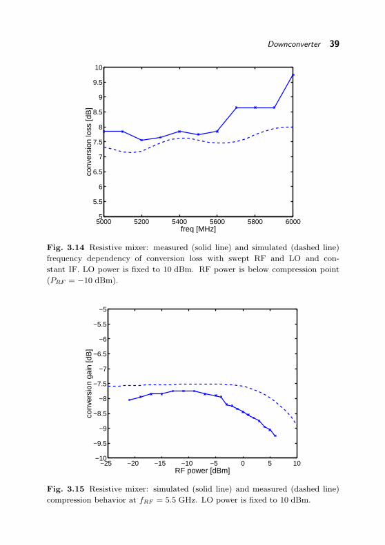
Downconverter 39
5000 5200 5400 5600 5800 60005
5.5
6
6.5
7
7.5
8
8.5
9
9.5
10
freq [MHz]
conv
ersi
on lo
ss [d
B]
Fig. 3.14 Resistive mixer: measured (solid line) and simulated (dashed line)
frequency dependency of conversion loss with swept RF and LO and con-
stant IF. LO power is fixed to 10 dBm. RF power is below compression point
(PRF = −10 dBm).
−25 −20 −15 −10 −5 0 5 10−10
−9.5
−9
−8.5
−8
−7.5
−7
−6.5
−6
−5.5
−5
RF power [dBm]
conv
ersi
on g
ain
[dB
]
Fig. 3.15 Resistive mixer: simulated (solid line) and measured (dashed line)
compression behavior at fRF = 5.5 GHz. LO power is fixed to 10 dBm.

40 Integrated circuit design
The restrictions of this transistor model leads to uncertainties in thesimulated large-signal behavior for this unusual operating conditions whichinclude the inverted operation. The mixer was designed with sufficientmargin and to meet the specifications of the system.
Fig. 3.16 shows the conversion gain of the integrated downconverterversus the applied LO power. As expected, the two additional amplifiersshift the curve compared to the resistive mixer alone: the LO amplifierreduces the required LO power by about 6 dB, while the IF amplifieradds 15 dB of gain, turning the conversion loss of the passive mixer intoconversion gain. Accordingly, a conversion gain of 7 dB is achieved at areduced LO power level of 5 dBm.
To characterize the linearity of the downconverter, 1 dB-compressionpoint and third-order intermodulation intercept point were measured. RFand LO were swept simultaneously, keeping the intermediate frequencyconstant at 1.45 GHz. The results are depicted in Fig. 3.17. For a LOpower of 10 dBm the compression and intercept point stay almost constantover frequency at around 1 dBm and 8 dBm, respectively. If the LO poweris reduced to 0 dBm, compression and intercept point at higher frequenciesdecrease. This indicates that, at these frequencies, the mixer becomes thelimiting element that constrains the system linearity, while at 5 GHz theconversion gain is sufficient to saturate the following amplifier.
−10 −5 0 5 10 15−15
−10
−5
0
5
10
LO power [dBm]
conv
ersi
on g
ain
[dB
] LO−amplifier
IF− amplifier
Fig. 3.16 Integrated downconverter with additional LO and IF amplifier (solid
line) compared to single passive mixer (dashed line). The IF amplifier provides
conversion gain, while the LO amplifier reduces the needed LO power.

Downconverter 41
The power consumption is 59 mA from a 3 V supply (177 mW) forthe two amplifiers. The passive mixer itself does not require DC power.Fig. 3.18 shows a chip micrograph of the integrated downconverter. Totalchip size is 1650 µm×900 µm.
5000 5200 5400 5600 5800 6000−5
0
5
10
15
frequency [MHz]
inpu
t pow
er [d
Bm
]
IP3
P1dB
Fig. 3.17 Integrated downconverter: input referred 1 dB-compression point
(crosses) IP3 (circles) for LO power of 0 dBm (dashed line) and 10 dBm (solid
line).
100 um
LO amplifier IF amplifier
mixer
Fig. 3.18 Chip micrograph of integrated downconverter. Total chip size is
1650 µm×900 µm (1.5 mm2).

42 Integrated circuit design
LNA stageswitchable
arrayelement
CAL LOnetworksdivider
IF
amplifiersresonant
image filterintegrated
resistivemixer
monolithic receiver
LNA stage2nd & 3rd
Fig. 3.19 Chip architecture of monolithically integrated receiver front-end.
3.4 Integrated front-end
3.4.1 Architecture
For the application in active antenna arrays, where the available spacebelow each antenna element is limited, further integration of the systemis needed. Fig. 3.19 shows the block diagram of the developed single-chipfront-end: it bases on the low-noise amplifier and integrated downcon-verter described in sections 3.2 and 3.3.
According to the system architecture an additional filter is needed tosuppress possible signals that could be received at the image frequency.This image filter is generally difficult to realize in any integrated tech-nology for two reasons: due to the process variations high-Q high-orderfilters cannot be build and, second, parasitic substrate coupling and on-chip cross-talk limit the achievable stop-band attenuation. In integratedreceivers often image-reject architectures are favored [40–43] to circumventthis problem. On the other hand, these architectures are very sensitiveto phase and amplitude imbalances of their complex mixer pairs, whichdegrade the image-rejection capability. Here, the selected intermediatefrequency at 1.45 GHz is sufficiently high to allow the use of a low-orderfilter. Therefore, it is decided to maintain the heterodyne concept avoid-ing the generation of a precise quadrature LO signal. The image filter isintegrated in the signal path between LNA and downconverter.
3.4.2 Switchable LNA
The active circuit components typically introduce amplitude and phasechanges that vary with ambient temperature, biasing and aging. For someantenna array applications, these variations need to be calibrated. Thiscalibration will be discussed later in chapter 5 in detail. This calibrationof the downconverter can be performed by switching between a precisely

Integrated front-end 43
E−FET
300
bondwires
ant
cal
to 2nd stage
degenerationsource
inductive
300µm
µm
0.5pF
2.3nH2pF
0.6nH
8pF 0.9pF
E−FET
Ω5k
2.3nH
matchinginput
Vg1
Vdd
g2V
100fF
Fig. 3.20 Circuit schematic of switchable LNA. Two identical input stages se-
lect between antenna and calibration signal. The drains are matched for the con-
dition that one transistor is biased on the gate and the other device is switched
off.
known reference signal (calibration mode) or the antenna input (receivingmode). Using a passive switch with a typical insertion loss of 1–2 dB [44]would significantly degrade the noise figure. Therefore a switchable low-noise amplifier is proposed. Thereby, it can be turned into an advantagethat, on an integrated circuit, closely spaced transistors show almost iden-tical electrical characteristics.
The first LNA stage consists of two symmetric 300 µm enhancementFETs connected at the drains as seen in Fig. 3.20. As in the previouslydescribed low-noise amplifier, inductive source feedback is used to improvethe linearity and increase the real part of the input impedance.
The impedance at the connected drains is strongly dependent on thestates of the two transistors. The interstage matching to the following twostages assumes that only one of the two devices is active. One transistoris biased for best linearity at a current density of Id/w=40 µA/µm, thesecond one is switched off by setting the gate bias to Vgs=0 V.
Differences in gain or phase of the two parallel input stages lead tocalibration errors. Therefore a completely symmetric layout is used. Thetransistors are located very close to each other and show the same gateorientation to avoid device mismatching.
It needs to be taken into account that the receive mode might be usedfor a long time, while the calibration requires a comparably short inter-val. Thermal effects on the devices need to be considered. To keep themon the same temperature, the transistors are physically connected at the

44 Integrated circuit design
drains. As a rough estimate, the following assessment can be made: ifboth transistors are thermally independent and the paths of heat trans-portation are limited to the way down through the substrate, the workingtransistor will heat up due to its losses, while the other stays at ambienttemperature. With a drain current of 7 mA at 3 V, a wafer thickness of25 mil (635 µm) and the thermal conductivity 0.5 W/Kcm of GaAs thecomputed temperature difference
∆T =1
0.5 W/Kcm·3 V · 7 mA
635 µm(3.6)
is less than 1 K. This indicates that thermal effects can be neglected inthis case.
A further crucial point is the large-signal behavior of the switch in off-state. As low-power enhancement FETs are used, a large input voltageexceeding the threshold voltage Vth switches the transistor on, thus de-grading the isolation. As the isolation is especially important for signalswith high input power levels, it is important to control this effect. To avoidthe use of negative control voltages the transistor width was increased tolower the input impedance and therefore also the voltage swing on thegate.
This approach leads to a trade-off between maximum tolerable inputpower and current consumption. It is assumed that a signal power largerthan the aimed 1 dB input compression point does not occur in practicaloperation, as in the system design it was determined to ensure that thereceiver always works in linear operation.
By choosing a wide transistor for this input stage, the input impedanceis lowered and it is ensured that the critical gate voltage is not exceededbelow an input power level of −20 dBm. Corresponding simulations werecarried out using the TOM3 large-signal model [39].
3.4.3 Image filter
The image filter consists of a third-order bandpass filter, realized withlumped elements according to Fig. 3.21. Since the filter is sensitive toparasitics, its layout was carefully optimized. The filter was designed fora higher bandwidth to allow for process variations.
The limitations in achieving high stop-band attenuation are internalcoupling and the absence of good grounding. On the semi-insulating GaAssubstrate magnetic coupling is the dominant coupling mechanism. Tominimize its effect on the stop-band attenuation, the input and outputinductors were separated by large distances.
The filter ground is not connected to the amplifier ground to minimizeany coupling over a common imperfect ground. By providing a number

Integrated front-end 45
5.7nH 5.7nH
image filter
151fF151fF
2.5pF
packageparasitic
test pads
600pH600pH
Lp
out
RFRF
in
Fig. 3.21 Schematic of lumped element image filter. T-type bandpass filter
with element values suited for monolithic integration. The implementation is
very sensitive to layout and package parasitics.
of bondwires to ground, the package parasitic Lp was kept sufficiently lownot to degrade the stop-band rejection. GSG-pads were added to permiton-wafer measurements of the filter alone.
3.4.4 Layout
High frequency circuit design usually employs the concept of wave portsrather than voltages and currents. S-parameters are used to characterizeall devices and elements with respect to input and output reference planes.This requires waveguide structures with a well-defined ground reference.On-chip test-structures typically employ a coplanar layout and all modelsare derived from these measurements.
At frequencies in the lower gigahertz range, the coplanar ground struc-ture usually is omitted to simplify the layout of complex circuits. Thisforces the ground current to take a different way, changing the componentbehavior. To maintain the validity of the models, this effects needs to beconsidered. If the geometrical distance of the additional ground path dmax
is significantly smaller than the minimum wavelength λmin involved, withdmax < 1
10λmin as a rule-of-thumb, the ground path is not needed to bemodelled as a distributed structure and can be replaced by appropriateinductances.
Here, the chip is bonded on a carrier substrate. Due to the missingground, all signals now refer to the waveguide ground on the substrate.The main problem then becomes to provide a good on-chip ground byusing as many bond-wire connections to the substrate as possible. Toobtain guidelines for the layout of a complex chip, the following simplifiedestimation is done:
If a device ”1” is connected to a row of pads bonded to ground, asseen in Fig. 3.22a, the bond-wires can be considered as inductances Lbond
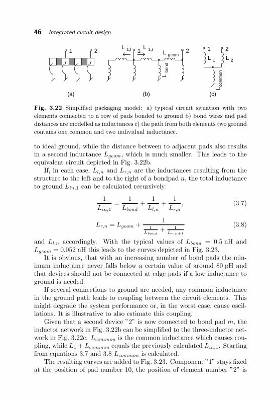
46 Integrated circuit design
1 1 22geomL
bond
L
(b) (c)(a)
L L 21
2 11,lL L 1,r
L com
mon
Fig. 3.22 Simplified packaging model: a) typical circuit situation with two
elements connected to a row of pads bonded to ground b) bond wires and pad
distances are modelled as inductances c) the path from both elements two ground
contains one common and two individual inductance.
to ideal ground, while the distance between to adjacent pads also resultsin a second inductance Lgeom, which is much smaller. This leads to theequivalent circuit depicted in Fig. 3.22b.
If, in each case, Ll,n and Lr,n are the inductances resulting from thestructure to the left and to the right of a bondpad n, the total inductanceto ground Lin,1 can be calculated recursively:
1
Lin,1=
1
Lbond+
1
Ll,n+
1
Lr,n, (3.7)
Lr,n = Lgeom +1
1Lbond
+ 1Lr,n+1
(3.8)
and Ll,n accordingly. With the typical values of Lbond = 0.5 nH andLgeom = 0.052 nH this leads to the curves depicted in Fig. 3.23.
It is obvious, that with an increasing number of bond pads the min-imum inductance never falls below a certain value of around 80 pH andthat devices should not be connected at edge pads if a low inductance toground is needed.
If several connections to ground are needed, any common inductancein the ground path leads to coupling between the circuit elements. Thismight degrade the system performance or, in the worst case, cause oscil-lations. It is illustrative to also estimate this coupling.
Given that a second device ”2” is now connected to bond pad m, theinductor network in Fig. 3.22b can be simplified to the three-inductor net-work in Fig. 3.22c. Lcommon is the common inductance which causes cou-pling, while L1 + Lcommon equals the previously calculated Lin,1. Startingfrom equations 3.7 and 3.8 Lcommon is calculated.
The resulting curves are added to Fig. 3.23. Component ”1” stays fixedat the position of pad number 10, the position of element number ”2” is

Integrated front-end 47
0 5 10 15 200
50
100
150
bondpad number
indu
ctan
ce [p
H]
Lcommon
total
inductance
10 pads
20 pads
L1+L
common
Fig. 3.23 Inductance to ground (solid lines) and common inductance (dashed
lines) vs. bond pad position for rows of 10 to 20 bond pads. For the common in-
ductance calculation it is assumed that one element is connected to pad number
10.
varied. If both components are connected to the same pad, the obtainedvalues obviously agrees with the previously calculated inductance. Themore the two connections are separated, the less the currents have to sharethe same way, Lcommon decays. A distance of three pads is sufficient tohalve the value.
Fig. 3.24 shows the chip micrograph of the receiver front-end. Thecircuit blocks are grouped along the ground pads. The ground of thesymmetric input stage and the consecutive stages are separated to avoidfeedback which would cause oscillations. The IF amplifier, which is lesssensitive to parasitic inductances due to its lower frequency, is located inthe center of the chip. Total chip size is 1650 µm×1950 µm.
3.4.5 Experimental results
The fabricated chip was bonded on a Duroid 6010 substrate and tested.Fig. 3.25 shows the measured conversion gain as a function of LO power.It saturates at 26.2 dB for LO levels higher than 0 dBm.
Fig. 3.26 shows the on-wafer measurement of the integrated image-filter compared to the simulations. The measured bandwidth is smaller,but still covers the signal band. The filter insertion loss is 6 dB and,therefore, higher than simulated. The stop-band attenuation is betterthan 35 dB.
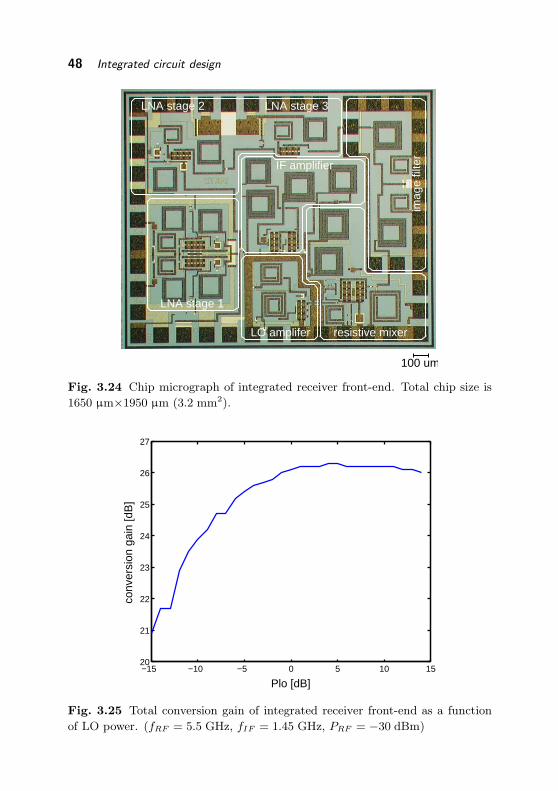
48 Integrated circuit design
imag
e fil
ter
resistive mixer
IF amplifier
LNA stage 1
LNA stage 2 LNA stage 3
100 um
LO amplifer
Fig. 3.24 Chip micrograph of integrated receiver front-end. Total chip size is
1650 µm×1950 µm (3.2 mm2).
−15 −10 −5 0 5 10 1520
21
22
23
24
25
26
27
Plo [dB]
conv
ersi
on g
ain
[dB
]
Fig. 3.25 Total conversion gain of integrated receiver front-end as a function
of LO power. (fRF = 5.5 GHz, fIF = 1.45 GHz, PRF = −30 dBm)

Integrated front-end 49
2 3 4 5 6 7 8 9 10−50
−45
−40
−35
−30
−25
−20
−15
−10
−5
0
S21
[dB
]
band
image
freq [GHz]
Fig. 3.26 Simulated (dashed line) and measured (solid line) frequency response
of the integrated image filter, measured on-wafer.
At frequencies higher than 8 GHz the attenuation rises less than pre-dicted by the simulations. This can be explained by parasitic couplingeffects.
To measure the frequency behavior of the whole chip, RF and LOfrequencies were swept, keeping fIF =1.45 GHz constant. The resultingcurves are depicted in Fig. 3.27: over the 5.125 GHz to 5.875 GHz range,the gain is above 20 dB. Image rejection is 36.7 dB at 5.125 GHz andraises to 50 dB at 5.875 GHz which is a very good result for an integratedreceiver.
Over the band of interest, the SSB noise figure is below 3.8 dB witha minimum of 3.3 dB at 5.6 GHz. The gain difference between the twoinput channels stays below 0.7 dB.
In order to determine the phase difference, an identical switchable LNAis fabricated on another chip. A vector network analyzer is utilized to de-termine the s-parameters in receive and calibration mode. The measuredcomplex gain curves are shown in Fig. 3.28. The maximal amplitude dif-ference is 0.5 dB, the maximal phase difference 4. Thereby it has tobe noticed that this also includes possible differences resulting from thetesting substrate and unequal bondwire lengths.

50 Integrated circuit design
5 5.2 5.4 5.6 5.8 6−40
−30
−20
−10
0
10
20
30
freq [GHz]
conv
ersi
on g
ain
[dB
]
0
1
2
3
4
5
6
7
SS
B n
oise
figu
re [d
B]
rejection image
Fig. 3.27 Frequency response of integrated receiver front-end: conversion gain
in receive (solid line) and calibration mode (dashed line), SSB noise figure (solid
line with dots) and gain at the corresponding image frequency (solid line with
triangles). (PLO = 10 dBm, PRF = −40 dBm).
−20 −10 0 10 20−20
−15
−10
−5
0
5
10
15
20
ch1
ch2
Fig. 3.28 Linear complex gain of the switchable low-noise amplifier integrated
on a separate chip. S21 of channel 1 (solid line with circles) and channel 2
(dashed line with crosses) from 5 to 6 GHz, one point every 50 MHz.

Integrated front-end 51
−30 −25 −20 −15 −10 −5 00
5
10
15
20
25
30
Pin [dBm]
gain
[dB
]
0
1dB compression
Fig. 3.29 Large signal behavior of integrated receiver front-end: gain of active
(solid line) and deactivated (dashed line) channel. The isolation is reduced at
input power levels higher than the 1 dB-compression point. (PLO = 10 dBm)
Fig. 3.29 shows the large signal behavior of the receiver frontend with10 dBm of LO power: 1 dB gain compression occurs at an input powerlevel of −18 dBm, which is higher than the specified −20 dBm. For areduced LO power of 0 dBm an input compression point of −20 dBm isobtained.
The switch isolation of the LNA is 17.65 dB at low power levels, de-creasing to 16.55 dB at the compression point. The expected degradationof the switch isolation occurs at input power levels higher than −15 dBm,which is above the compression point. Signals of this power level are notexpected to occur and, therefore, the degradation has no practical signif-icance.
For an LO power of 5 dBm the compression point and third-order in-termodulation intercept point (∆f=100 kHz) are measured for differentfrequencies and depicted in Fig. 3.30. At 5.4 GHz, where the highest con-version gain occurs, the compression point drops slightly below −20 dBmfor this LO power level.
To investigate the immunity against interferers, the blocking behaviorof the circuit is measured: a sinusoidal signal at the center of the RF-band (5.5 GHz) and a power clearly below the input compression point(−50 dBm) is applied to the receiver input. It is then converted by thereceiver front-end (fLO = 6.95 GHz, PLO = 5 dBm) to the intermediate
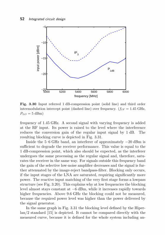
52 Integrated circuit design
5000 5200 5400 5600 5800 6000−25
−20
−15
−10
−5
frequency [MHz]
inpu
t pow
er [d
Bm
]
P1dB
IP3
Fig. 3.30 Input referred 1 dB-compression point (solid line) and third order
intermodulation intercept point (dashed line) over frequency. (fIF = 1.45 GHz,
PLO = 5 dBm)
frequency of 1.45 GHz. A second signal with varying frequency is addedat the RF input. Its power is raised to the level where the interferencereduces the conversion gain of the regular input signal by 1 dB. Theresulting blocking curve is depicted in Fig. 3.31.
Inside the 5–6 GHz band, an interferer of approximately −20 dBm issufficient to degrade the receiver performance. This value is equal to the1 dB-compression point, which also should be expected, as the interfererundergoes the same processing as the regular signal and, therefore, satu-rates the receiver in the same way. For signals outside this frequency bandthe gain of the selective low-noise amplifier decreases and the signal is fur-ther attenuated by the image-reject bandpass-filter. Blocking only occurs,if the input stages of the LNA are saturated, requiring significantly morepower. The reactive input matching of the very first stage forms a lowpassstructure (see Fig. 3.20). This explains why at low frequencies the blockinglevel almost stays constant at −6 dBm, while it increases rapidly towardshigher frequencies. Above 9.6 GHz the blocking could not be measured,because the required power level was higher than the power delivered bythe signal generator.
In the same graph in Fig. 3.31 the blocking level defined by the Hiper-lan/2 standard [15] is depicted. It cannot be compared directly with themeasured curve, because it is defined for the whole system including an-

Integrated front-end 53
0 2 4 6 8 10 12−30
−25
−20
−15
−10
−5
0
5
10
15
20
freq [GHz]
inpu
t pow
er [d
Bm
]IF
RF
LO fimage
Fig. 3.31 Blocking experiment: interferer power-level that is needed to decrease
the regular signal conversion gain by 1 dB. Blocking-power level (solid line)vs.
frequency and Hiperlan/2 blocking mask [15] (dashed line). (PLO = 5 dBm)
tennas, modulation and coding: interferer signals falling within this maskare not allowed to cause more than 10% erroneously received ”protocoldata units (PDUs)”. However, the blocking measured in this analog fash-ion is a good indication of the expected performance. For frequencies lessthan 2.5 GHz the measured blocking curve falls below the mask. Thisis not considered as a problem for the system, as the antenna acts as abandpass filter with a significant attenuation at low frequencies.
In Tab. 3.2 the circuit performance at 5.5 GHz is compared with re-cently published results of other integrated 5–6 GHz receivers. The re-ceiver front-end reaches state-of-the-art performance. The noise figureis very low if it is considered that both receivers that reach similar val-ues [45,46] require external components whose losses were subtracted fromthe measurements.
The circuit draws 55 mA for the signal path (LNA, mixer and IF am-plifier) and 21 mA for the additional LO amplifier, resulting in a total of76 mA from a 3 V supply (230 mW). Total chip size is 1650 µm×1950 µm(3.2 mm2).

54 Integrated circuit design
Table 3.2 Circuit performance at 5.5 GHz (PLO = 10 dBm) compared to re-
cently published integrated 5–6 GHz receivers
frequency gain im. rej. Pin,1dB NF
[40] 5.2 GHz 26 dB >50 dB −18 dBm 7.2 dB(vgain)
[47] 5.3 GHz 14 dB 36 dB −15 dBm 6.8 dB(tuned)
[41] 5.2 GHz 43 dB 62 dB −26.5 dBm 6.4 dB(vgain)
[42] 5 GHz 19 dB >40 dB −22 dBm 5.9 dB[43] 5.5 GHz 17 dB 80 dB −14 dBm 5.1 dB
(5.3–5.8) (tuned)[45] 4.7 GHz 24 dB 35 dB −23 dBm 3.2 dB[46] 5.25 GHz 8.7 dB n.a. −21 dBm 3 dB(DSB)this work 5.5 GHz 26 dB 48 dB -18 dBm 3.3 dB
(5.2-5.9)
3.5 Power amplifier
The power amplifier represents a critical part in most systems, because it isone of the building blocks with the highest power consumption. Its mono-lithic integration is often problematic, because the devices must be drivento their electrical and thermal limits. This opens interesting questionsconcerning the calibration of transmit arrays, especially when the systemtransmits in bursts and the amplifiers are switched off during times ofinactivity. This motivates the design of a power amplifier to address thisissue, although it is not directly needed for the receiving antenna. Theimplications for transmit arrays will be discussed in chapter 5.4.
3.5.1 Design
One advantage of multiple antenna systems is that the total transmitpower is shared by all elements. In a N element array this reduces theoutput power of a single amplifier by N if the total power is kept constant,or by N2 if the additional antenna gain is considered. In a four elementarray, therefore, the individual power amplifier output power is reducedby 6 dB or 12 dB, respectively. This leads to medium power amplifierswhich are easier to integrate. The output power chosen here is 20 dBm.(For comparison: Hiperlan/2 [15] requires a total radiated power higherthan −15 dBm, but not more than 23 dBm at 5.2 GHz and 30 dBm at5.8 GHz.)

Power amplifier 55
0 1 2 3 4 5 60
50
100
150
200
250
300
drain voltage [V]
drai
n cu
rren
t [m
A]
load−line
supply voltage
Vdmax
Idmax
Fig. 3.32 I/V characteristic of 1200 µm D-FET for different gate source volt-
ages Vgs (solid line) and construction of optimal load line (dashed line) for
maximal output power.
Fig. 3.32 shows the I/V-characteristic of a depletion FET with theload line for maximum output power. Idmax is given by the device itself,Vdmax results from the supply voltage Vdd and the knee voltage Vknee. Theoutput power of a given device can be maximized by increasing the supplyvoltage until Vmax reaches the breakdown voltage. Here, a supply voltageof 3 V is maintained; the device width is changed to adjust the maximalcurrent. The saturation power at the output can be estimated as
Pmax =1
8(Vdd − Vknee) Idmax (3.9)
The device is scaled to a width of 1200 µm, leading to a Pmax of roughly23 dBm, which leaves some margin for implementation losses.
The schematic of the last amplifier stage is shown in Fig. 3.33. Theoutput matching network performs a transformation to present the rightload impedance to the intrinsic transistor. Thereby, the transistor para-sitics are taken into account. For more details on this technique it is re-ferred to [48]. The input is matched to the source using conjugate complexmatching. Additional parallel and series resistors are needed to guaranteeunconditional stability.
A special network is designed to enable switching of the amplifier.In principle there are two ways to switch a power amplifier: the supply

56 Integrated circuit design
stabilization&
input matching
PA switch
RF in
+3V
loadline matching
RF out
temp sensor
Q1
Q2
Fig. 3.33 Schematic of the power amplifier output stage. The power ampli-
fier can be switched off to save power when the system is not transmitting.
A Schottky diode is integrated close to the transistor to monitor the thermal
behavior.
voltage at the drain is removed, or the gate-source voltage Vgs is reducedbelow the pinch-off voltage. Switching the large currents at the source ordrain introduces significant losses, which decreases the efficiency.
If the device is switched by the gate voltage, another difficulty arises:in on-state the gate bias voltage should be set with a low impedance at lowfrequencies. Otherwise self-biasing and memory effects occur [49], whichlead to signal distortion in non-constant envelope systems. On the otherhand, the switching signal should be well isolated from the RF signal toavoid unwanted cross-talk. The use of large capacitors has to be avoidedto keep the resulting time constants and switching times low.
In this amplifier the power device Q1 (D-FET) is selected for its con-venient optimum gate bias point of Vgs = 0 V. This allows to use an aux-iliary transistor Q2 to provide a low-impedance short-circuit from gate toground, if switched on. The remaining on-state resistance is not criticalfor the circuit performance, because a certain resistive load is needed atthe gate to stabilize the device. For negative control voltages, the aux-iliary transistor closes and the gate of the main device is tied down bylarge-value resistor. This upper limit of the resistance is determined toavoid unintended switch opening like discussed above in 3.4.2.
A diode is integrated in close vicinity to the power device as a tem-perature monitor. With raising temperature its diffusion voltages Vd de-creases. If a constant current is impressed, the actual diode temperatureT is determined as
T = T0V0
V, (3.10)

Power amplifier 57
0 2 4 6 8 10−20
−15
−10
−5
0
5
10
15
20
frequency [GHz]
gain
[dB
]/ re
turn
loss
[dB
]S
21
S22
S11
Fig. 3.34 Measured S-parameters of the power amplifier: return loss S11 (solid
line with crosses), S22 (solid line with diamonds) and gain S21 (dashed line with
circles).
where V is the measured temperature across the diode and V0 is the knownvoltage at the reference temperature T0.
The power amplifier consists of two stages, whereby the driver stagedevice width is half of the output device width. The compression behavioris mainly determined by the last stage.
3.5.2 Experimental results
The power amplifier was bonded on a test substrate and measured. Fig. 3.34shows the measured S-parameters. The input matching is better than−15 dB over the 5–6 GHz band. The output matching is around −10 dBand does not show a pronounced matching frequency, which is typical forload-line matched amplifiers. This also explains why the gain peak occursbelow the design band. The small-signal gain inside the band is more than10 dB. At small signal operation the amplifier draws 500 mW from a 3 Vsupply.
Fig. 3.35 shows the compression behavior at 5.2 GHz. At 1 dB gaincompression the amplifier delivers 19 dBm. It is remarkable that the rela-tive phase shift at the compression point is below 0.7, which demonstratesthat the amplifier can be used up to the compression point without intro-ducing significant AM/PM conversion.

58 Integrated circuit design
−5 0 5 10 150
2
4
6
8
10
12
14
16
18
20
input power [dBm]
gain
[dB
], ph
ase
[deg
]
gain
phase
1dBcompression
Fig. 3.35 Compression behavior of power amplifier: gain (solid line) and phase
(dashed line) vs. input power at 5.2 GHz.
3.5.3 Pulsed operation
In the literature a typical gain change of −0.015 dB/C for GaAs cir-cuits [50] is reported. Therefore, it can be expected, that the amplifiershows a varying gain, when it is used in pulsed operation exhibiting chang-ing temperatures. To quantify this effect the amplifier is switched on andoff with a period of 7×250 µs = 1.75 ms with a varying duty-cycle, corre-sponding to typical IEEE 802.11a or Hiperlan/2 data bursts. The voltageacross the temperature sensor diode is monitored.
The resulting gain and temperature are depicted in Fig. 3.36. Ata duty-cycle of 0/7 the amplifier is at ambient temperature. With in-creasing duty-cycle the temperature rises linearly to 55 C at continu-ous transmission. With a measured power dissipation of 333 mW of thelast stage a thermal resistance of 99 K/W results (calculated thermal re-sistance through the 4 mil GaAs substrate is 197 K/W). Changing theduty-cycle from 1/7 to 7/7, the gain drops more than 0.5 dB, resulting ina gain change of 0.019 dB/K with temperature.
To evaluate the dominating thermal time-constants, the amplifier isswitched on for single pulses of different length, assuming that the am-plifier is at ambient temperature at the beginning of the pulse. Fig. 3.37shows the temperature graph for a 20 ms pulse. The measured curveagrees very well with the simple exponential model
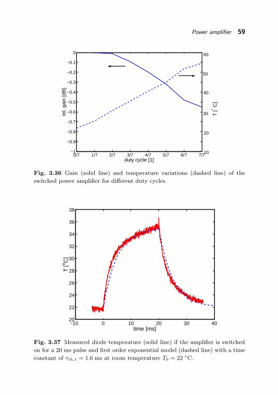
Power amplifier 59
0/7 1/7 2/7 3/7 4/7 5/7 6/7 7/7−1
−0.9
−0.8
−0.7
−0.6
−0.5
−0.4
−0.3
−0.2
−0.1
0
duty cycle [1]
rel.
gain
[dB
]
20
T [° C
]
30
40
50
60
10
Fig. 3.36 Gain (solid line) and temperature variations (dashed line) of the
switched power amplifier for different duty cycles.
−10 0 10 20 30 4020
22
24
26
28
30
32
34
36
38
time [ms]
T [o C
]
Fig. 3.37 Measured diode temperature (solid line) if the amplifier is switched
on for a 20 ms pulse and first order exponential model (dashed line) with a time
constant of τth,1 = 1.6 ms at room temperature T0 = 22 C.

60 Integrated circuit design
T (t) =
T0 + ∆T ·(1 − exp( t
τth,1))
0 ≤ t ≤ 20 ms
T0 + ∆T · exp(− t−20 msτth,1
) t > 20 ms
, (3.11)
assuming a thermal time constant of τth,1 = 1.6 ms and a temperaturedifference of ∆T = 13 K. For shorter pulse lengths no lower time constantis found.
Comparing the maximum temperature of 35 C with the 55 C mea-sured at continuous operation, another time-constant must be present.Repeating the above measurement with longer pulse lengths, a secondtime constant of τth,2 = 2200 ms is found. The two time-constants canbe attributed to the small heat capacity of the device and the thermalresistance of the GaAs substrate and die-attach on the one hand, and themounting patch and the heat transfer to the environment on the otherhand.
Knowing this thermal behavior, the temperature change at the begin-ning of a pulse is
∂
∂tT (t)
∣∣∣∣t=0
=∆T1
τth,1+
∆T2
τth,2= 8667 K/s + 10 K/s, (3.12)
which leads to an approximate gain change rate of
∂
∂tg(t)
∣∣∣∣t=0
= −8676 K/s · 0.017 dB/K = −148 dB/s. (3.13)
This expected change of gain, although it is fairly low considering thetypical 250 µs pulse length, opens the question how a possible calibrationwill be affected. This behavior can be further investigated using systemmeasurements, which will be reported in chapter 5.4.
3.6 10.7–11.7 GHz SiGe downconverter
As already mentioned in section 3.1.1, the advance of silicon-based tech-nologies makes them an interesting for RF applications. To achieve a fastanalog circuits, the standard CMOS process can be extended by a SiGeheterojunction bipolar transistor (HBT). This allows the complete inte-gration of mixed-signal circuits. By aggressive vertical and lateral scaling,transit frequencies as high as 375 GHz could be reached [31], making thistechnology competitive with classical RF processes.
In the same way as wireless LANs move now from 2.4 GHz to 5 GHzto achieve higher data rates, it can be foreseen that the wireless local loop
10.7–11.7 GHz SiGe downconverter 61
(WLL), which offers fixed wireless links to the public phone network, willmove from 3.5 GHz to 11 GHz for the same reason.
At this frequency, a low-noise amplifier with a noise figure as lowas 2 dB was demonstrated [51], using an advanced SiGe process withfT = 80 GHz.
For the envisioned application, it is advantageous to use a low-ft pro-cess, which relaxes the requirements of the lithography and helps to mini-mize the manufacturing costs. On such processes with ft of about 50 GHz,low noise amplifiers with 3.3 dB noise figure [52] and active mixers [53]were demonstrated, up to 17 and 20 GHz [54, 55]. Even a receiver front-end at 24 GHz [56] is reported.
All proposed circuits employ Gilbert-type active mixers, which leadsto limited dynamic ranges. Input compression points up to −9 dBm withsingle sideband noise figures at best of 12 dB are reached. To mitigatethe noise contribution of the mixer, a pre-amplifier is needed. The com-pression point is lowered further and the frontend becomes more sensibleto intermodulation and blocking phenomena. It was already seen abovefor the 5 GHz receiver, that a resistive mixer can be used to enhance thedynamic range. On a SiGe process, the MOSFET device can be employedto realize this passive FET mixer, as it will be described below.
The goal of this study is to develop a downconverter for the 10.7 –11.7 GHz band with specifications similar to those of the presented 5 GHzreceiver.
3.6.1 IBM 6HP SiGe BiCMOS process
The IBM 6HP process is based on a 0.25 µm standard CMOS process.Processing steps are added to obtain HBTs, which are available as high-speed or high-breakdown devices for power applications. The high-speeddevice reaches a transit frequency of 47 GHz. To allow low-loss passivedevices in spite of the conductive substrate, a thick dielectric and top-levelmetal are added as last steps [57]. The key parameters of this process aresummarized in Tab. 3.3.
3.6.2 Low-noise amplifier
The main difference between the LNA design on GaAs as described in3.2 and the realization on this SiGe process are the higher losses that areassociated with the passive components, while the transit frequency of thedevices of 47 GHz is more than two times higher. If the same strategy isfollowed and common-source stages are cascaded using conjugate complexinterstage-matching, it is found that a large part of the gain deliveredby the transistors is dissipated in the passive matching networks. At a

62 Integrated circuit design
Table 3.3 IBM-6HP process key parameters (from [57])
Element Parameter Value
SiGe HBT current amplification β 100transit frequency ft 47 GHz
max. freq. of oscillation fmax 65 GHzspiral inductor inductance 0.28nH..83nH
quality factor 19 @ 10GHzMIM capacitor capacitance per area 0.70 fF/µm2
1.38nH
55fF
1.27nH
2x 20µm
µ 2x 20µm
Vcc
155pH
RF
out
120fF
RF
in2x 20 m
Fig. 3.38 Circuit schematic of two stage 11 GHz low-noise amplifier. The first
stage uses inductive source degeneration for noise matching and a cascode topol-
ogy for maximal gain. The second stage uses a single transistor to enable output
matching. Biasing networks are not shown here.
center frequency of 11.2 GHz, the gain of the first stage is critically low,compromising the overall noise figure.
To circumvent this problem, a different circuit concept is used, shownin Fig. 3.38: a cascode topology as input stage provides a sufficiently highgain. Again inductive source degeneration is applied to achieve a higherreal part of the input impedance. The problem associated with the cascodestructure is the high output impedance. A transformation to the 50 Ω portimpedance over a certain bandwidth would require a multi-stage networkwith high associated losses, consuming the gain advantage of the cascodestage. To achieve a simple output matching, a second single-transistorstage is added. At the interface between the two stages no impedancetransformation is introduced, only the reactance is compensated to achievea gain peak in the center of the band.
A coplanar-like layout was chosen: all unused space was filled with

10.7–11.7 GHz SiGe downconverter 63
8 9 10 11 12 13 14−30
−25
−20
−15
−10
−5
0
5
10
15
20
freq [GHz]
gain
/ret
urn
loss
[dB
]S21
NF S22
S11
Fig. 3.39 Simulated (dashed lines), measured (solid lines) S-parameters and
noise figure NF (dots) of 11 GHz LNA
patches of metal, which are connected among each other, forming a groundmesh.
Fig. 3.39 shows the simulated and measured S-parameters of the manu-factured amplifier: The gain peak of 14.8 dB is less than the simulated19 dB. Both input and output return loss are better than −10 dB andagree reasonably well with the simulations. The measured noise figure islower than 4 dB. The measured compression behavior depicted in Fig. 3.40indicates a 1 dB-compression point of −12.7 dBm. The power consump-tion is 6.4 mA from a 3.3 V supply (21 mW). The chip micrograph isshown in Fig. 3.41. The chip size is 1323 µm×923 µm (1.2 mm2).

64 Integrated circuit design
−30 −25 −20 −15 −1010
10.5
11
11.5
12
12.5
13
13.5
14
14.5
15
input power [dBm]
gain
[dB
]
Fig. 3.40 Compression behavior of 11 GHz LNA at 11.2 GHz. Gain vs. input
power (solid line) and 1 dB-compression point (dashed line).
in outRFRF
V cc
Fig. 3.41 Chip micrograph of 11 GHz low noise amplifier. The total chip size
is 1323 µm×923 µm.
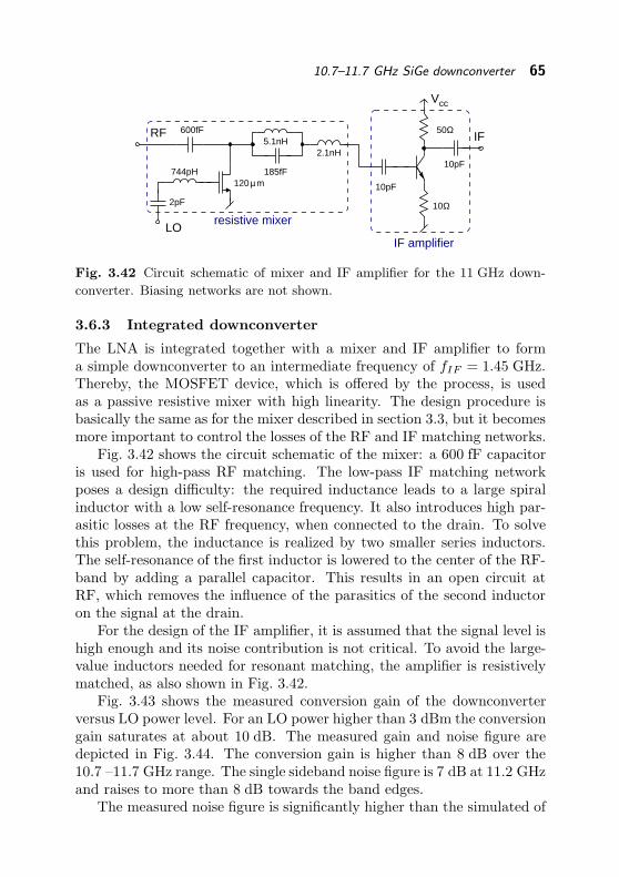
10.7–11.7 GHz SiGe downconverter 65
Vcc
2pF
600fF
µ120 m
5.1nH
10pF744pH
50Ω
10Ω
10pF
2.1nH
IF amplifier
resistive mixer
185fF
LO
RF IF
Fig. 3.42 Circuit schematic of mixer and IF amplifier for the 11 GHz down-
converter. Biasing networks are not shown.
3.6.3 Integrated downconverter
The LNA is integrated together with a mixer and IF amplifier to forma simple downconverter to an intermediate frequency of fIF = 1.45 GHz.Thereby, the MOSFET device, which is offered by the process, is usedas a passive resistive mixer with high linearity. The design procedure isbasically the same as for the mixer described in section 3.3, but it becomesmore important to control the losses of the RF and IF matching networks.
Fig. 3.42 shows the circuit schematic of the mixer: a 600 fF capacitoris used for high-pass RF matching. The low-pass IF matching networkposes a design difficulty: the required inductance leads to a large spiralinductor with a low self-resonance frequency. It also introduces high par-asitic losses at the RF frequency, when connected to the drain. To solvethis problem, the inductance is realized by two smaller series inductors.The self-resonance of the first inductor is lowered to the center of the RF-band by adding a parallel capacitor. This results in an open circuit atRF, which removes the influence of the parasitics of the second inductoron the signal at the drain.
For the design of the IF amplifier, it is assumed that the signal level ishigh enough and its noise contribution is not critical. To avoid the large-value inductors needed for resonant matching, the amplifier is resistivelymatched, as also shown in Fig. 3.42.
Fig. 3.43 shows the measured conversion gain of the downconverterversus LO power level. For an LO power higher than 3 dBm the conversiongain saturates at about 10 dB. The measured gain and noise figure aredepicted in Fig. 3.44. The conversion gain is higher than 8 dB over the10.7 –11.7 GHz range. The single sideband noise figure is 7 dB at 11.2 GHzand raises to more than 8 dB towards the band edges.
The measured noise figure is significantly higher than the simulated of
66 Integrated circuit design
approximately 3.5 dB. This is attributed to the fact that both, the low-noise amplifier and the resistive mixer, show significantly higher lossesthan simulated. It can be estimated that the signal gain from the systeminput to the output of the mixer is less than 5 dB and, therefore, thecontribution of the resistively matched IF amplifier to the overall noisefigure is significantly higher than intended.
Fig. 3.45 shows the measured compression behavior. The 1 dB inputcompression point of −14 dBm is higher than simulated. This can beexplained by the lower gain of the pre-amplifier. It is expected that thedownconverter noise figure can be reduced by adding a simple gain stagebetween LNA and mixer.
In Tab. 3.4 the performances in terms of noise figure and linearity aresummarized and compared to other published results. Where no explicitvalues were given, the input compression points as well as the single side-band noise figures were estimated from the given values. These estimatedvalues are stated in brackets.
Fig. 3.46 shows a picture of the downconverter. The mixer and ampli-fier were added to the reused layout of the low-noise amplifier in Fig. 3.41.The total chip size is 1323 µm×1323 µm (1.75 mm2). The power con-sumption is 27.6 mA from a 3.3 V supply (80 mW).
−10 −5 0 5 10 156
6.5
7
7.5
8
8.5
9
9.5
10
10.5
11
LO power [dBm]
conv
ersi
on g
ain
[dB
]
Fig. 3.43 Conversion gain of integrated downconverter at 11.2 GHz vs. LO
power. (PRF = −30 dBm)

10.7–11.7 GHz SiGe downconverter 67
10.8 11 11.2 11.4 11.60
2
4
6
8
10
12
freq [GHz]
gain
/NF
[dB
]
gain SSB−NF
Fig. 3.44 Conversion gain (solid line) and single-sideband noise figure (dashed
line with crosses) of the downconverter vs. frequency. LO power is 5 dBm, RF
power −20 dBm.
−30 −25 −20 −15 −10 −52
3
4
5
6
7
8
9
10
11
12
RF input power [dBm]
conv
ersi
on g
ain
[dB
]
Fig. 3.45 Compression behavior (solid line) of the downconverter at 11.2 GHz
and LO power of 5 dBm and 1 dB-compression point (dashed line).

68 Integrated circuit design
Table 3.4 Published downconverters on 50 GHz-ft SiGe processes. Values in
brackets were not given explicitly and are estimations.
work function P1dB,input NF (SSB)
[53] 11.2 GHz mixer (−15.5 dBm) 12.4 dB[54] 17 GHz mixer (−19.6 dBm) (14.5 dB)[55] 20 GHz mixer (−9 dBm) (20 dB)[56] 24 GHz front-end −32.3 dBm (>9dB )
this work 11 GHz front-end -14 dBm 7 dB
inRF LO
in
IFout
VVrf if
Fig. 3.46 Chip micrograph of downconverter. Mixer and downconverter are
added to LNA (compare Fig. 3.41). Total chip size is 1323 µm×1323 µm.

Conclusions 69
3.7 Conclusions
This chapter describes the design of a 5–6 GHz monolithically integrateddownconverter for the use in antenna arrays. It is found that the chosenclassical heterodyne architecture in this case is able to compete with otherapproaches. In particular it was possible to reach an image rejection of48 dB which is a good value for integrated circuits. This performance isbasically limited by parasitic on-chip coupling. Good linearity and a lowsystem noise-figure could be combined by the use of a resistive mixer.
To enable a calibration of the downconverter without introducing aswitch and the associated losses at the input, a switchable low-noise am-plifier is proposed. A gain and phase difference of less than 0.5 dB and 4
is demonstrated.A medium output-power power-amplifier is designed and its thermal
behavior is studied. It is used later in chapter 5.4 to study the practicalimplications in multiple antenna systems.
An integrated 11 GHz downconverter is demonstrated on a low-ft SiGeprocess to explore future directions. A MOSFET device is used as aresistive mixer to obtain low-noise and a good linearity. Although theimplementation losses are higher than expected, a reasonable performanceis reached.


4
Passive array
This chapter focuses on the design of the passive antenna structure. Thechoice of aperture-coupled patch antennas is motivated first. An equiva-lent circuit model is developed, which helps to efficiently design this type ofantenna for given specifications. It is demonstrated that this antenna canbe modified to provide a differential interface towards modern integratedcircuit technologies.
The integration of antennas into an array is discussed, and the effect ofmutual coupling is considered. It is shown that this coupling can be com-pensated for the proposed array. The equivalent circuit model is extendedfrom the single antenna to the whole array by including the mutual cou-pling. Last, it is experimentally demonstrated, that the mutual couplingcan be reduced, if the antenna-interface in an active array is optimized.
4.1 Antenna design
4.1.1 Choice of antenna structure
To select an appropriate antenna structure, it is necessary to define thespecific needs for the application in an active array:
• The antenna has to operate over the specified bandwidth, here from5.15 to 5.875 GHz. A frequency selective antenna is preferred over abroadband structure, because it pre-filters all out-of-band interferers.
• The antenna should be small in geometrical size. An antenna spacingof λ0/2 from center-to-center must be possible.
• The antenna should have a low directivity, so that the array patternis dominated by the steering function and not by the pattern of theindividual elements.
• For flexibility the antenna should allow both orthogonal polarizations.
• The antenna structure should be easy and cheap to fabricate and ithas to be compatible with monolithically integrated circuits (MMICs).

72 Passive arrays
matching
stub
patch
circuit
substrateantenna
slot
substrate
ground plane
Fig. 4.1 Exploded sketch of aperture-coupled patch antenna; separate sub-
strates can be individually selected for circuit and antenna, magnetic coupling
is achieved by a slot in the common ground plane.
All these specifications are fulfilled by the aperture-coupled patch an-tenna [58], although the required relative bandwidth of more than 13% isat the upper limit of what can be achieved with this structure [59].
4.1.2 Aperture-coupled patch antenna
The demands on microstrip substrates are contradictory for the designof circuits and antennas [59]: to achieve good radiation properties anda large bandwidth a thick substrate with a low dielectric constant εr isneeded. If passive structures like filter, coupler and transmission linesare implemented, radiation has to be avoided. This requires a thin highεr substrate, which confines the electric field to the dielectric materialbetween conductors and ground plane. This conflict can be resolved byusing two independent substrates for circuit and antenna as shown inFig. 4.1.
The antenna patch is printed on a thick, low-εr substrate, while thecircuit resides on a thin, high εr substrate. Both are mounted togetherand share the same ground plane. There are several ways to excite thepatch: capacitive, magnetic coupling or probe feeding. Magnetic couplingis proposed, because it can be achieved by etching a slot in the commonground plane and therefore maintaining a simple planar structure [58].
Numerical tools have to be used to simulate and optimize the antenna,which involves a high computational effort. To gain more insight into theinfluence of the single parameters, and therefore reduce the number ofneeded simulation runs, a lumped-element circuit model was developed.Using this modelling approach, the design can be speeded up significantly.

Antenna design 73
couplingmagnetic
resonator
planereference
Fig. 4.2 Equivalent circuit of aperture-coupled patch antenna: a resonator is
magnetically coupled to the transmission line.
a) single resonator model
R
Lp
p
L
R
s
sel1l el2l
b) double resonator model
pC sC
Fig. 4.3 Single (a) and double resonator (b) equivalent circuit to model the
electrical behavior of the three dimensional antenna structure
4.1.3 Modelling
Microstrip structures can accurately be modelled, including losses, disper-sive behavior and end-effects [60]. These models are widely known andavailable in all modern microwave circuit design tools. Therefore, it isadvantageous to separate the design process into the optimization of thepatch and slot structure, and the determination of the microstrip feedingand matching-structure, respectively. This reduces the parameter-spacefor the computational expensive field simulations.
Placing a port at both ends of the microstrip-line, the structure canbe considered as a resonator coupled to a transmission line as shown inFig. 4.2. In [61] the equivalent circuit is simplified to a parallel RLCresonator in series with an inductor, as shown in Fig.4.3a. For the ge-ometries and materials used in this work, a two resonator model as shownin Fig.4.3b models the antenna behavior more accurately over a broaderfrequency range.
Fig.4.4 shows the simulated insertion loss of the antenna structure incomparison with both models: it is obvious, that the second resonanceat around 7.5 Ghz cannot be described by the single resonator model.Furthermore the two resonator model is more accurate inside the operatingbandwidth from 5 to 6 GHz.
So far, all model parameters can be determined from magnitude simu-lations (or measurements) and no precise phase information is necessary.

74 Passive arrays
4 4.5 5 5.5 6 6.5 7 7.5 8−25
−20
−15
−10
−5
0
freq [GHz]
inse
rtio
n lo
ss [d
B]
Fig. 4.4 Transmission coefficient of simulated antenna sructure(solid), one res-
onator model (dashed with boxes) and two resonator model (dashed with circles)
If the full wave simulation is deembedded and the reference planes forboth ports are shifted to the center of the slot, the transmission functionexhibits an additional phase shift of around 20 at 5.5 GHz. In the modelthis is accounted for by adding two ideal transmission lines of correspond-ing lengths lel1 and lel2 at the input and output.
4.1.4 Design method
Considering the antenna structure described above and the two resonatormodel in Fig. 4.3 it is not possible to postulate a general relationshipbetween the geometrical parameters and the values of the equivalent cir-cuit. Nevertheless, it is possible to evaluate the sensitivity of the circuitvalues to certain geometrical changes [62]. This provides several usefuldependencies:
• As expected, varying the patch size changes the resonance frequencyof the first resonator formed by Rp, Lp and Cp. This determines theoperating frequency of the antenna.
• The size, geometry and orientation of the slot determines the cou-pling of the antenna resonator to the microstrip line. An increasedcoupling leads to a higher value Rp, but also to a higher characteristicimpedance X0 = jω0Lp = (jω0Cp)
−1. It is found that the qualityfactor Q stays nearly constant with different sizes and positions.

Antenna design 75
• Increasing the slot size not only gives a higher coupling, but alsolowers the resonance frequency of the second resonator, formed byRs, Ls and Cs. This indicates, that the second resonance is relatedto the slot structure.
• Different shapes of the slot lead to different quality factors Q of thefirst resonance.
• Change of thickness or dielectric constant εr of the patch substrateleads to both, a change of the quality factor and the first resonatorsresonance frequency.
From the above, one advantage of this modelling approach becomes visible:the quality factor, which is related to the maximum achievable antennabandwidth, varies only with different slot shapes or antenna substrates.For a given combination it can be evaluated once, using a single fieldsimulation.
Therefore, the following design procedure is suggested: first, adequateslot shape and substrate type are selected for the aimed antenna band-width. From several slot types proposed in [58] the “dogbone” slot is foundto provide the highest bandwidth. High bandwidth can also be achievedby choosing a thick, low-εr substrate Once the combination is fixed, theresonator coupling is set by adjusting the slot. Generally the coupling ishigher for a slot centered in the middle of the patch, where the highestcurrent occurs. A higher coupling is also obtained by increasing the slotsize. Moreover, it is advantageous to keep the slot resonance frequency ashigh as possible. If the slot gets into resonance, it radiates to both sides ofthe ground plane, thus degrading the front-to-back ratio of the antenna.Next, the antenna center frequency is adjusted by varying the patch size.And last, the length of the matching stub is calculated to compensate theinductive part, that remains at the center frequency of the first resonator.
Fig. 4.5 shows a typical simulated input matching of the matched an-tenna structure. It demonstrates the typical design trade-off between re-turn loss and matching bandwidth: the trajectory of the reflection coef-ficient in the Smith chart circles around the matching point. This cir-cle reaches its highest impedance at the patch resonance, the impedanceequals Rp of the equivalent circuit. With equivalent coupling, an Rp of50 Ω and therefore a very low return loss at the center frequency couldbe achieved. If a certain return loss is tolerated, the Rp can be furtherincreased, resulting in a higher bandwidth. A typical requirement for an-tennas is a voltage standing-wave ratio (VSWR) of lower than 2. Thiscorresponds to an input return loss of approximately −10 dB.
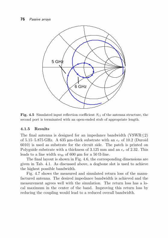
76 Passive arrays
5 GHz
6 GHz
Fig. 4.5 Simulated input reflection coefficient S11 of the antenna structure, the
second port is terminated with an open-ended stub of appropriate length.
4.1.5 Results
The final antenna is designed for an impedance bandwidth (VSWR≤2)of 5.15–5.875 GHz. A 635 µm-thick substrate with an εr of 10.2 (Duroid6010) is used as substrate for the circuit side. The patch is printed onPolyguide substrate with a thickness of 3.125 mm and an εr of 2.32. Thisleads to a line width w50 of 600 µm for a 50 Ω-line.
The final layout is shown in Fig. 4.6, the corresponding dimensions aregiven in Tab. 4.1. As discussed above, a dogbone slot is used to achievethe highest possible bandwidth.
Fig. 4.7 shows the measured and simulated return loss of the manu-factured antenna. The desired impedance bandwidth is achieved and themeasurement agrees well with the simulation. The return loss has a lo-cal maximum in the center of the band. Improving this return loss byreducing the coupling would lead to a reduced overall bandwidth.
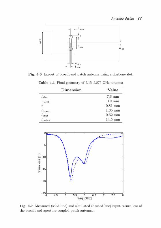
Antenna design 77
l inset
w 50
l pat
ch
l slot
r
stublslotw
Fig. 4.6 Layout of broadband patch antenna using a dogbone slot.
Table 4.1 Final geometry of 5.15–5.875 GHz antenna
Dimension Value
lslot 7.6 mmwslot 0.9 mmr 0.81 mmlinset 1.35 mmlstub 0.62 mmlpatch 14.5 mm
4 4.5 5 5.5 6 6.5 7 7.5 8−25
−20
−15
−10
−5
0
freq [GHz]
retu
rn lo
ss [d
B]
Fig. 4.7 Measured (solid line) and simulated (dashed line) input return loss of
the broadband aperture-coupled patch antenna.
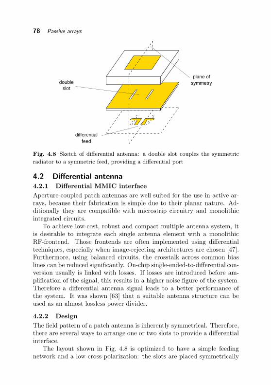
78 Passive arrays
doubleslot
feeddifferential
plane ofsymmetry
Fig. 4.8 Sketch of differential antenna: a double slot couples the symmetric
radiator to a symmetric feed, providing a differential port
4.2 Differential antenna
4.2.1 Differential MMIC interface
Aperture-coupled patch antennas are well suited for the use in active ar-rays, because their fabrication is simple due to their planar nature. Ad-ditionally they are compatible with microstrip circuitry and monolithicintegrated circuits.
To achieve low-cost, robust and compact multiple antenna system, itis desirable to integrate each single antenna element with a monolithicRF-frontend. Those frontends are often implemented using differentialtechniques, especially when image-rejecting architectures are chosen [47].Furthermore, using balanced circuits, the crosstalk across common biaslines can be reduced significantly. On-chip single-ended-to-differential con-version usually is linked with losses. If losses are introduced before am-plification of the signal, this results in a higher noise figure of the system.Therefore a differential antenna signal leads to a better performance ofthe system. It was shown [63] that a suitable antenna structure can beused as an almost lossless power divider.
4.2.2 Design
The field pattern of a patch antenna is inherently symmetrical. Therefore,there are several ways to arrange one or two slots to provide a differentialinterface.
The layout shown in Fig. 4.8 is optimized to have a simple feedingnetwork and a low cross-polarization: the slots are placed symmetrically
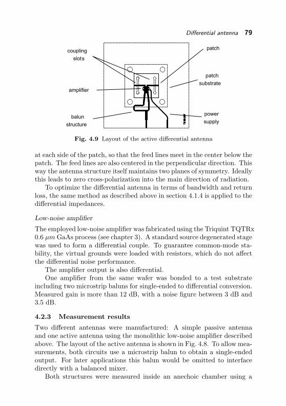
Differential antenna 79
TB
02-0
37
patchcoupling
slots
power
supplybalun
structure
amplifier
patch
substrate
Fig. 4.9 Layout of the active differential antenna
at each side of the patch, so that the feed lines meet in the center below thepatch. The feed lines are also centered in the perpendicular direction. Thisway the antenna structure itself maintains two planes of symmetry. Ideallythis leads to zero cross-polarization into the main direction of radiation.
To optimize the differential antenna in terms of bandwidth and returnloss, the same method as described above in section 4.1.4 is applied to thedifferential impedances.
Low-noise amplifier
The employed low-noise amplifier was fabricated using the Triquint TQTRx0.6 µm GaAs process (see chapter 3). A standard source degenerated stagewas used to form a differential couple. To guarantee common-mode sta-bility, the virtual grounds were loaded with resistors, which do not affectthe differential noise performance.
The amplifier output is also differential.One amplifier from the same wafer was bonded to a test substrate
including two microstrip baluns for single-ended to differential conversion.Measured gain is more than 12 dB, with a noise figure between 3 dB and3.5 dB.
4.2.3 Measurement results
Two different antennas were manufactured: A simple passive antennaand one active antenna using the monolithic low-noise amplifier describedabove. The layout of the active antenna is shown in Fig. 4.8. To allow mea-surements, both circuits use a microstrip balun to obtain a single-endedoutput. For later applications this balun would be omitted to interfacedirectly with a balanced mixer.
Both structures were measured inside an anechoic chamber using a

80 Passive arrays
Narda 642 standard gain horn. The measured gain in Fig. 4.10 showsabout 5.5 dBi gain for the passive structure. The active antenna has 14 dBito 17 dBi over the 5–6 GHz band. Both curves show some ripple overfrequency which is due to the presence of the connectors.
For comparison with a standard system, where antenna and amplifierare separated, the transducer gain of the embedded amplifier can be cal-culated if the gain of the active antenna and of a passive reference areknown [64]. The computation using the averaged gain curves lead to 10to 12 dB gain over the band.
Fig. 4.11 shows the measured and simulated pattern of the active an-tenna at 5.8 GHz. The agreement between measurement and simulationis good regarding the co-polarization. The antenna pattern was found tobe similar over the whole band. The sensitive measurement of the cross-polarization is influenced by the near connectors. Therefore, it differs fromthe simulated pattern, but the cross-polarization rejection of better than27 dB is very low. The measured front-to-back ratio is higher than 8 dB.
Fig. 4.12 shows a photography of the manufactured active antenna.The size of the whole antenna is 50.8 mm × 50.8 mm, the antenna sub-strate is 25.4 mm × 25.4 mm.
4.5 5 5.5 6 6.5 70
5
10
15
20
freq/GHz
ante
nna
gain
[dB
i]
active
passive
Fig. 4.10 Measured gain of active differential antenna (solid line) compared to
passive reference (dashed line).

Differential antenna 81
30
210
60
240
90
270
120
300
150
330
180 0
co−polarization
0 −10 −20
cross−pol.
[dB]
Fig. 4.11 Measured (solid line) co- and cross-polarized pattern of active differ-
ential antenna compared to simulations (dashed line).
Fig. 4.12 Circuit and radiator-side photography of active differential antenna.
The size of the whole antenna is 50.8 mm × 50.8 mm, the antenna substrate is
25.4 mm × 25.4 mm.
82 Passive arrays
4.3 Antenna arrays and mutual coupling
4.3.1 Non-ideal arrays
A practical antenna has certain geometrical extensions and therefore dif-fers from the idealized point source. The field radiated by an antenna canbe roughly seperated into three regions:
• Reactive near field: this region close to the antenna structure is dom-inated by field components that drop off with 1/r3 or higher orderswith increasing distance r from the antenna. It contains electromag-netic energy, which is not radiated to the free space. If any object isintroduced into this zone, the directional pattern, but also the feed-point impedance, are changed.
• Radiating near field: this region, also called Fresnel zone, does notcontain significant amounts of reactive energy. It is characterized byfield components with radial dependency. Objects introduced herelead to a change of the directional pattern, but the antenna matchingis not noticeably changed.
• Radiating far field, or Fraunhofer region: the radiated wave in thisregion equals an ideal spherical wave: the field pattern does not varywith increasing distance, only the field energy decreases with 1/r2. Ata certain distance this wave appears as an almost planar wave-front.
The terminals in a communication systems typically are sufficiently sepa-rated to assume far-field operation. The dominant spherical wave justifiesthe use of the quasi-optical model.
The main difficulty arises when the antennas are moved together tofulfil the spatial Nyquist condition d ≤ λ/2: the necessary maximumdistance lies in the range of the geometrical antenna size, clearly insidethe extension of the reactive near field. The resulting mutual coupling isan important effect in antenna arrays, which can not be neglected and willbe discussed more detailed below.
Furthermore, in a practical system the antennas have to be mountedon some support with finite extensions. Radiated waves reaching theseedges are diffracted. Following the geometrical model, these edges act likeparasitic sources, which can not be controlled independently, causing achange of the radiation pattern.
It is important for a correct operation of any antenna array to main-tain the precise phase and amplitude relationships of all elements. Thisis especially a problem in active arrays, where components with certainvariations are used. Chapter 5 addresses the possible calibration methodsto eliminate this effect.

Antenna arrays and mutual coupling 83
4.3.2 Classification
The mutual coupling in antenna arrays has various effects, spanning fromthe displacement of diagram zeros over changes of input matching to theoccurrence of blind angles. Antenna arrays showing mutual coupling canbe classified into some subcategories.
If two antennas are separated in a way, that the reactive near-field (seesection 4.3.1) is not noticeably changed by the presence of the neighborelement, it can be assumed that the far field pattern also stays unchanged.Under this assumption of well-behaved antennas, the pattern of an elementembedded into an array is identical with the pattern of an isolated elementgi:
g(φ) ≈ gi(φ). (4.1)
Well-behaved arrays can be obtained using small antenna elements or largespacings.
A second important criteria is, whether a unique radiation mode ofeach element can be associated with the according terminal voltage. Ifthis condition is fulfilled, an array can be modelled with respect to theelectrical states at its ports [65].
Without regarding the actual field distributions it can be distinguishedbetween weak coupling and strong coupling, which refers to a measurableeffect at the antenna ports. If
Z =
z11 . . . z1N
.... . .
...zN1 . . . zNN
(4.2)
is the impedance matrix of the array, the electrical behavior can be de-scribed by the vector equation
V = ZI, (4.3)
with
V =
v1
...vN
and I =
i1...
iN
being the terminal voltage and current vectors. In a weakly coupled arraymutual impedances zij (i 6= j) are present, but they do not influence theimpedance seen into one of the ports. In a strongly coupled array this

84 Passive arrays
Table 4.2 Categories of antenna arrays with mutual coupling
Category Effect
well behaved embedded pattern does not changesingle moded a unique mode pattern can be asso-
ciated with each port voltagestrong/ weak coupling input impedances depend on steer-
ing angleblind angles excitation of surface waves, no radi-
ation possible for certain angles
is not the case; the mutual impedance also changes the port impedance.The so-called active impedance of the m-th element is defined as
Zm =vm
im=
N∑
n=1
inim
· zmn. (4.4)
According to Eqn. 4.4, the active impedance depends on the actual exci-tation of the array, as the ratio in/im changes with moving steering angle.This can lead to a significant reduction of the radiated power. In theworst case, the active input reflection coefficient Γm reaches |Γm| = 1 forcertain angles. In this case a surface wave along the antenna elements isexcited and no energy can be radiated. This phenomenon is called blindangle and needs to be avoided in practical applications.
The different categories of antenna arrays are summarized in Tab. 4.2.Dependent on the type of mutual coupling, the effects on the array oper-ation are also different (a single-mode relationship is assumed):
• A well behaved, weakly coupled array shows deformed patterns, ifone array element is measured alone. This is due to the parasiticexcitation of the neighbor elements. In a synthesized array patternthis results in shifted and degraded diagram zeros and sidelobes. Thecoupling effect can be compensated (see section 4.3.3) to obtain thesimple model of uncoupled antennas (pattern multiplication).
• If the array is weakly coupled, but not well behaved, the far-fieldpattern of each element might be different. Thus, a transformation ofthe port signals is not sufficient to obtain the simple array description.In large arrays, all inner elements have an identical environment. Thisleads to similar embedded element patterns gemb(φ). Using these,instead of the isolated element patterns gi(φ), it is again possible toapply the simple pattern multiplication principle [66]. To achieve
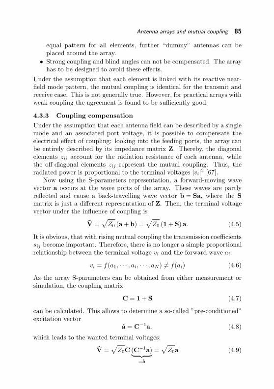
Antenna arrays and mutual coupling 85
equal pattern for all elements, further “dummy” antennas can beplaced around the array.
• Strong coupling and blind angles can not be compensated. The arrayhas to be designed to avoid these effects.
Under the assumption that each element is linked with its reactive near-field mode pattern, the mutual coupling is identical for the transmit andreceive case. This is not generally true. However, for practical arrays withweak coupling the agreement is found to be sufficiently good.
4.3.3 Coupling compensation
Under the assumption that each antenna field can be described by a singlemode and an associated port voltage, it is possible to compensate theelectrical effect of coupling: looking into the feeding ports, the array canbe entirely described by its impedance matrix Z. Thereby, the diagonalelements zii account for the radiation resistance of each antenna, whilethe off-diagonal elements zij represent the mutual coupling. Thus, theradiated power is proportional to the terminal voltages |vi|
2 [67].Now using the S-parameters representation, a forward-moving wave
vector a occurs at the wave ports of the array. These waves are partlyreflected and cause a back-travelling wave vector b = Sa, where the Smatrix is just a different representation of Z. Then, the terminal voltagevector under the influence of coupling is
V =√
Z0 (a + b) =√
Z0 (1 + S)a. (4.5)
It is obvious, that with rising mutual coupling the transmission coefficientssij become important. Therefore, there is no longer a simple proportionalrelationship between the terminal voltage vi and the forward wave ai:
vi = f(a1, · · · , ai, · · · , aN ) 6= f(ai) (4.6)
As the array S-parameters can be obtained from either measurement orsimulation, the coupling matrix
C = 1 + S (4.7)
can be calculated. This allows to determine a so-called ”pre-conditioned”excitation vector
a = C−1a, (4.8)
which leads to the wanted terminal voltages:
V =√
Z0C (C−1a)︸ ︷︷ ︸=a
=√
Z0a (4.9)

86 Passive arrays
vertically polarized horizontally polarized
Fig. 4.13 Four element aperture-coupled patch antenna array with vertical or
horizontal polarization. Arrows show orientation of radiated E-field.
4.3.4 Array of aperture-coupled patch antennas
So far, no assumption has been made on the field pattern of the elements.To verify if aperture-coupled patch antennas can be used to form a well-behaved array (see section 4.3.2), a vertical and a horizontal polarizedconfiguration are investigated as shown in Fig. 4.13. The center-to-centerantenna spacing in both cases is 27.3 mm, which is approximately λ0/2 atthe center frequency of 5.5 GHz.
Both arrays are simulated using a commercial field simulator (Agi-lent HFSS v5.6). The structures are first driven with the ideal excitationvectors for each element:
a1 =
1000
,a2 =
0100
, · · ·
The resulting far-field patterns at 5.5 GHz are depicted in Fig. 4.14 and4.15 for vertical and horizontal polarization, respectively. In both casesall patterns show some deformations, which is a typical effect of mutualcoupling. The aperture size of single element is not sufficient to explain thespatial frequency of the superimposed ripple. This indicates, that furtherradiation sources must be present.
The simulated S-parameter transmission coefficients si(i+1) betweentwo adjacent elements, which are often used to characterize the strengthof mutual coupling, are −14 dB for the vertical polarized and −17 dB forthe horizontal polarized array.
Using the simulated S matrices, the pre-conditioned excitations a1, a2, · · ·are calculated and applied to both arrays. Thereby, the de-embedded S′
matrix is referred to a reference plane in the center of the slot, whereasEqn.4.9 refers to the phase center of the antenna. Empirically it is foundthat the deembedding distance needs to be increased by 40 electricallength at 5.5 GHz. The same value can be validated, if the coupling ma-trix is estimated from a transformation of the far-field (see chapter 5).
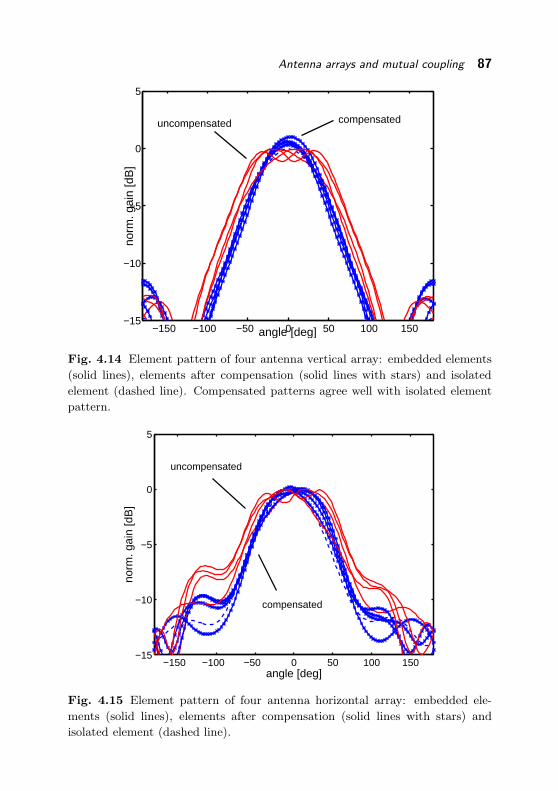
Antenna arrays and mutual coupling 87
−150 −100 −50 0 50 100 150−15
−10
−5
0
5
angle [deg]
norm
. gai
n [d
B]
compensated uncompensated
Fig. 4.14 Element pattern of four antenna vertical array: embedded elements
(solid lines), elements after compensation (solid lines with stars) and isolated
element (dashed line). Compensated patterns agree well with isolated element
pattern.
−150 −100 −50 0 50 100 150−15
−10
−5
0
5
angle [deg]
norm
. gai
n [d
B]
compensated
uncompensated
Fig. 4.15 Element pattern of four antenna horizontal array: embedded ele-
ments (solid lines), elements after compensation (solid lines with stars) and
isolated element (dashed line).

88 Passive arrays
−150 −100 −50 0 50 100 150−35
−30
−25
−20
−15
−10
−5
0
5
10
15
angle [deg]
norm
. gai
n [d
eg]
compensated uncompensated
ideal
Fig. 4.16 Four element vertical polarized array with uniform distribution,
steered to 30: uncompensated (solid line), compensated (solid line with stars)
and ideal (dashed line) pattern.
The resulting embedded element patterns are added to Fig. 4.14 andFig. 4.15. The agreement of embedded patterns and isolated pattern isgood over the relevant range of −90 ≤ φ ≤ +90. An array with elementsmounted 45-slanted shows similar results. For this type of arrays, thisjustifies the assumption of well-behaved antennas.
To demonstrate the effect on beamforming, a uniform excitation |ai| = 1is chosen. To remove the possible cancelling of effects due to the symme-try of the structure, the beam is steered to +30 by setting the excitationvector to
a =
1i−1−i
.
In Fig. 4.16 the ideal far-field pattern calculated by pattern multiplica-tion, and the patterns resulting from an excitation with a and the pre-conditioned a = C−1a are compared. It is seen that mutual coupling leadsto a shift and degradation of the pattern zeros and a slight change of theside-lobe levels with respect to the ideal pattern. Pre-conditioning of theexcitation vector compensates for these changes and restores reasonable

Antenna arrays and mutual coupling 89
p
R
s
sel1l l
C
stub
C
L
L
R
L
C
p
p s
s
s
l stub
Cp
Ls
l el1port 2
port 1
feed 1
feed 2
M, ∆τ
Fig. 4.17 Extension of aperture-coupled patch antenna model: a retarded cou-
pling inductance models the mutual coupling.
low pattern zeros. Outside the relevant range of −90 ≤ φ ≤ +90 thepattern is dominated by diffraction effects.
4.3.5 Array coupling model
The compensation of mutual coupling described above assumes a matchedantenna element showing a purely resistive input impedance. Strictly, thisis only valid in the center of the operating bandwidth.
To describe the array behavior over a broader bandwidth the aperture-coupled patch-antenna model proposed in section 4.1.4 is extended to mu-tual coupling: given that the resonance frequency of the second resonator(RS ,LS and CS) is sufficiently high, the radiated power of each antennaelement equals the power dissipated in the resistors RP . These, therefore,are replaced by ”radiation”ports with an impedance of Z = RP as shownin Fig.4.17.
To model the mutual coupling different forms and combinations ofinductive and capacitive coupling were explored. The best agreement wasachieved using a retarded coupling inductance
V2 = (jωM · exp(−jω∆τ)) I1 (4.10)
between all inductors LP of adjacent elements. Fitting the model to fieldsimulations, a ∆τ of 33 ps is found, which equals a free-space propagationdistance of around 10 mm. It is also observed that the model parameterof the single antenna element do not have to be changed significantly.
Fig. 4.18 shows the S-parameter transfer function between two adja-cent antennas gained from this model compared to a full field simulationusing HFSS. The model approximates this function over a broader range.
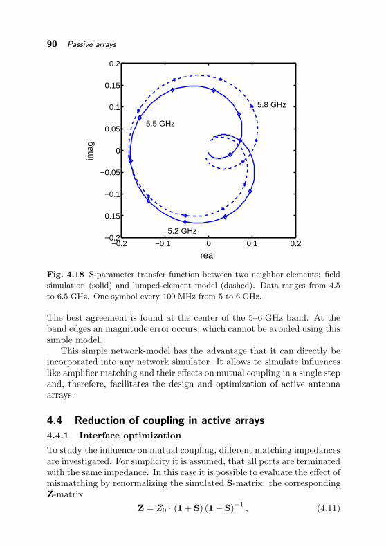
90 Passive arrays
−0.2 −0.1 0 0.1 0.2−0.2
−0.15
−0.1
−0.05
0
0.05
0.1
0.15
0.2
real
imag
5.5 GHz
5.8 GHz
5.2 GHz
Fig. 4.18 S-parameter transfer function between two neighbor elements: field
simulation (solid) and lumped-element model (dashed). Data ranges from 4.5
to 6.5 GHz. One symbol every 100 MHz from 5 to 6 GHz.
The best agreement is found at the center of the 5–6 GHz band. At theband edges an magnitude error occurs, which cannot be avoided using thissimple model.
This simple network-model has the advantage that it can directly beincorporated into any network simulator. It allows to simulate influenceslike amplifier matching and their effects on mutual coupling in a single stepand, therefore, facilitates the design and optimization of active antennaarrays.
4.4 Reduction of coupling in active arrays
4.4.1 Interface optimization
To study the influence on mutual coupling, different matching impedancesare investigated. For simplicity it is assumed, that all ports are terminatedwith the same impedance. In this case it is possible to evaluate the effect ofmismatching by renormalizing the simulated S-matrix: the correspondingZ-matrix
Z = Z0 · (1 + S) (1− S)−1 , (4.11)

Reduction of coupling in active arrays 91
−80 −60 −40 −20 0 20 40 60 80−15
−10
−5
0
5
angle [deg]
norm
. gai
n [d
B]
isolated
90 Ohm
25 Ohm
Fig. 4.19 Second element in a four element vertical polarized antenna array:
elements terminated with 50 Ω (solid line), 25 Ω (crosses), 90 Ω (diamonds)
and isolated element (dashed line). A low termination impedance reduces the
coupling.
leads to the renormalized matrix S′ using the new normalization impedanceZnew:
S′ =
(1
ZnewZ + 1
)−1 (1
ZnewZ − 1
). (4.12)
Then, the new coupling matrix C′ is given by
C′ =
√Z0
Znew(1 + S′) . (4.13)
In a system with a nominal impedance of Z0 a certain mismatch usuallycan be tolerated, as long as the power transfer is not significantly degraded.This condition can be fulfilled by a range of termination impedances. Areturn loss of 10 dB, for example, is approximately achieved by a termina-tion impedance of 25 Ohm or 90 Ohm. The difference between these twoterminations and 50 Ohm as a reference value is investigated further.
The directional patterns that results from the excitation of the secondelement in a four element vertical polarized array are calculated for allthree impedances. They are depicted in Fig. 4.19, where they are alsocompared to the isolated element pattern. For all three impedances aneffect of mutual coupling is visible that leads to a deformation of the
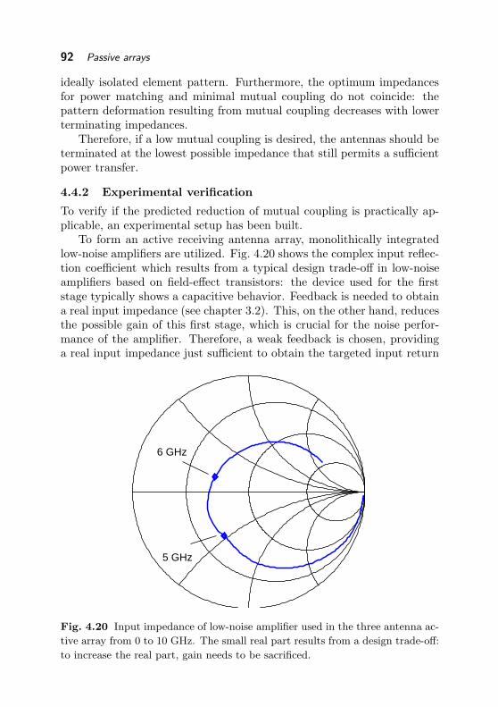
92 Passive arrays
ideally isolated element pattern. Furthermore, the optimum impedancesfor power matching and minimal mutual coupling do not coincide: thepattern deformation resulting from mutual coupling decreases with lowerterminating impedances.
Therefore, if a low mutual coupling is desired, the antennas should beterminated at the lowest possible impedance that still permits a sufficientpower transfer.
4.4.2 Experimental verification
To verify if the predicted reduction of mutual coupling is practically ap-plicable, an experimental setup has been built.
To form an active receiving antenna array, monolithically integratedlow-noise amplifiers are utilized. Fig. 4.20 shows the complex input reflec-tion coefficient which results from a typical design trade-off in low-noiseamplifiers based on field-effect transistors: the device used for the firststage typically shows a capacitive behavior. Feedback is needed to obtaina real input impedance (see chapter 3.2). This, on the other hand, reducesthe possible gain of this first stage, which is crucial for the noise perfor-mance of the amplifier. Therefore, a weak feedback is chosen, providinga real input impedance just sufficient to obtain the targeted input return
5 GHz
6 GHz
Fig. 4.20 Input impedance of low-noise amplifier used in the three antenna ac-
tive array from 0 to 10 GHz. The small real part results from a design trade-off:
to increase the real part, gain needs to be sacrificed.

Reduction of coupling in active arrays 93
low−noise amplifier
l trafo
Fig. 4.21 Layout of the three element active receiving array. Different lengths
ltrafo lead to a high and a low impedance at the antenna phase center.
loss.Integrating this amplifier into an array of vertically polarized antennas,
as shown in Fig. 4.21, the actual impedance at the antenna feed dependson the distance ltrafo between amplifier and feed. At 5.5 GHz the ampli-fier has a return loss of −8 dB. To present a purely real impedance atthe antenna phase center, line lengths ltrafo of 8 mm and 13.5 mm arerequired, if the additional electrical distance of 40 from the feeding pointis taken into account (see section 4.3.3). The resulting impedances areapproximately 22 Ω and 116 Ω, respectively.
Both structures are simulated using a network simulator. The coupledarray model proposed in section 4.3.5 is used and combined with the mea-sured S-parameters of the low-noise amplifier. The coupling matrix C canbe evaluated by simply simulating the transfer functions from the inter-nal antenna ports to the three output ports. To obtain results which areindependent of the amplifier gain, the results can be divided by this gain.This leads to quantities which are directly comparable to the measureds21 between two elements in a passive array, which is a usual measurefor the characterization of mutual coupling. For the center element, thenormalized coupling coefficient is
ccoupl =c12
c22(4.14)
The coupling coefficients for both transformation distances ltrafo are shownin Fig. 4.22.
For the center frequency of 5.5 GHz, this model predicts a significantlyreduced mutual coupling for the arrangement showing a low impedance atthe antenna. This reduction is limited to a certain bandwidth, as the linetransformation is frequency dependent.
Both arrays were manufactured and their far-field radiation patternswere measured in an anechoic chamber. For comparison with the simula-tions, the coupling matrix C is computed from the far-field data using the

94 Passive arrays
4.5 5 5.5 6 6.5−24
−22
−20
−18
−16
−14
−12
−10
mag
nitu
de o
f cou
plin
g co
eff.
[dB
]
freq [GHz]
8 mm
13.5 mm
Fig. 4.22 Mutual coupling coefficient c12/c22 simulated (dashed line) and ex-
tracted from measurements (solid line) for the two amplifier line lengths.
Fourier transformation method, which is described in chapter 5. The re-sulting coupling coefficients are added to Fig. 4.22. The limited frequencyrange is due to the lack of measurement data towards higher frequenciesand the constrained range of the transformation (d ≤ λ/2). The resultsagree qualitatively with the simulations, but a growing difference appearsat the end of the antenna bandwidth. This is explained by the fact thatthe circuits, in this roll-off region, show the highest sensitivity to possibletolerances. Any deviations from the idealized model, like edge diffraction,reflections, or disturbance from the connectors, lead to an error in thecalculation of C.
However, both, simulation and far-field measurement, demonstratethat the right choice of the array termination impedance leads to a sig-nificantly reduced mutual coupling (simulated s21 with a termination of50 Ω is −14 dB) at the center frequency. This is also confirmed by themeasured active patterns of the center element in both arrays, shown inFig. 4.23. The array terminated with the lower impedance clearly showsan improved pattern compared to the other array.

Conclusions 95
15
20
25
30
30
210
60
240
90
270
120
300
150
330
180 0
Fig. 4.23 Measured directional pattern of the center element of the three an-
tenna array at 5.46 GHz, absolute gain (antenna and amplifier) in dBi. LNA
is mounted at different distances to present a low (solid line) or a high (dashed
line) impedance. For the low impedance the pattern is less degraded by mutual
coupling.
4.5 Conclusions
In this chapter the design of the passive array was discussed. A lumped-element equivalent circuit model for aperture-coupled patch antennas sim-plifies the design for given specifications. A symmetric antenna structureis proposed to provide a differential electrical interface, which is attractivefor the integration of the antenna with integrated circuits.
The mutual antenna coupling is studied and it is found that aperture-coupled patch-antenna arrays can be approximated by loosely coupledisolated elements. This well-behaved array condition allows to remove theeffect of the coupling.
An extension of the proposed equivalent circuit enables the simulationof mutual coupling using a network simulator. By suitable impedancemismatch on antenna arrays, the mutual coupling can be reduced to acertain extend. This is demonstrated by a standard low-noise amplifier

96 Passive arrays
mounted with an optimized electrical distance between amplifier and an-tenna. This method, so far, is limited to a certain bandwidth. It is possibleto improve its bandwidth by choosing a different line impedance or by aproper amplifier design.

5
Calibration
This chapter discusses the main aspects of antenna array calibration. Itstarts with a review of the known methods based on far-field sources andtest-tones. A novel method is added, which allows to reduce the com-plexity of the calibration network. Last, the dynamic performance is in-vestigated. This becomes important when parts of the active circuits areswitched on and off and alter their characteristics, as it occurs in poweramplifiers.
5.1 Problem formulation
Most array processing techniques assume a set of independent sensors,which measure the phase and amplitude of the electromagnetic field attheir locations without influencing it. Practical antenna systems at giga-hertz frequencies show several deviations from this idealized signal model:
• To avoid grating lobes, sensor distances half of the signal wavelength,or lower, are required. The low spacing causes mutual coupling be-tween the antennas.
• Finite ground planes introduce metal edges, which diffract arrivingwaves. They act as parasitic elements and alter the array pattern.
• The active hardware, including amplifiers and mixers, exhibit gainand phase variations. These depend on fabrication tolerances, biasing,temperature and aging.
• Cables and connectors are a further source of phase and amplitudevariations. Generally, their sensitivity to mechanical stress rises withthe frequency of operation.
A calibration is needed to find a mapping between the real antennaarray and and the idealized sensor model. Thereby, also the practicalfeasibility of a calibration method is an important selection criteria. Twogeneral methods can be distinguished: those, that use separate antennasand calibrate via the air interface and those, which use internal calibrationsignals.

98 Calibration
resonant matching
CL
R l
Rq
Fig. 5.1 Two element resonant power matching for Rl ≥ Rq
5.1.1 Active circuit variations
The practical difficulty to obtain identical and time-constant transfer func-tions is illustrated in the following simplified example: Fig. 5.1 shows atwo stage resonant power matching between a source impedance Rq and aload Rl. This circuit represents the typical input matching of a transistoramplifier with the capacitance C, or a fraction of it, being the gate-sourcecapacitance of the device. If Rl ≥ Rq are given, the values L and C foroptimal power transfer can be calculated:
L =1
ω0
√RqRl − R2
q (5.1)
C =1
ω0
√1
RqRl−
1
R2l
, (5.2)
where ω0 = 2πf0 is given by the center frequency f0. Strictly, optimummatching is obtained only for this frequency. The practically usable band-width depends on the quality factor Q of the matching network. In thiscase it is defined as
Q =ωL
Rq= ωCRl =
√Rl
Rq− 1 (5.3)
and depends on the impedance transformation ratio Rl/Rq. If it is nowassumed that C is dominated by the intrinsic capacitances of a transistor,it may strongly vary from the ideal value. Intuitively it is clear that thetransfer function from the source to the load resistor is affected stronger,the higher the quality factor is. To give a quantitative example, the am-plitude and phase changes caused by the capacitance variation are givenin Fig. 5.2 and Fig. 5.3 for different quality factors.
For element variations of ±25% or more, which are not uncommon inmonolithic circuit fabrication, significant amplitude and especially phaseerrors are obtained.

Problem formulation 99
50 75 100 125 150−2
−1.8
−1.6
−1.4
−1.2
−1
−0.8
−0.6
−0.4
−0.2
0
element variation [%]
ampl
itude
var
iatio
n [d
B]
1
2 3
Fig. 5.2 Amplitude changes caused by variations of the capacitor C for different
quality factors of the matching network.
50 75 100 125 150−40
−30
−20
−10
0
10
20
30
40
element variation [%]
phas
e va
riatio
n [o ]
1
2
3
Fig. 5.3 Relative phase changes caused by variations of the capacitor C for
different quality factors of the matching network.
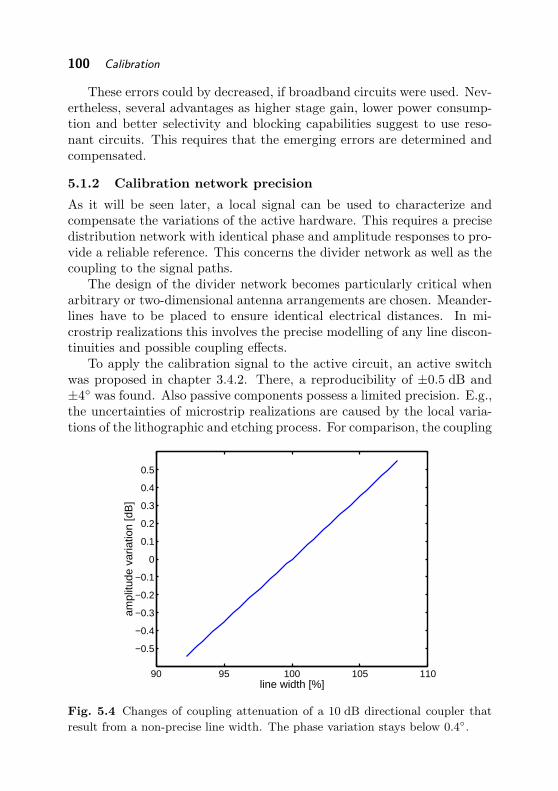
100 Calibration
These errors could by decreased, if broadband circuits were used. Nev-ertheless, several advantages as higher stage gain, lower power consump-tion and better selectivity and blocking capabilities suggest to use reso-nant circuits. This requires that the emerging errors are determined andcompensated.
5.1.2 Calibration network precision
As it will be seen later, a local signal can be used to characterize andcompensate the variations of the active hardware. This requires a precisedistribution network with identical phase and amplitude responses to pro-vide a reliable reference. This concerns the divider network as well as thecoupling to the signal paths.
The design of the divider network becomes particularly critical whenarbitrary or two-dimensional antenna arrangements are chosen. Meander-lines have to be placed to ensure identical electrical distances. In mi-crostrip realizations this involves the precise modelling of any line discon-tinuities and possible coupling effects.
To apply the calibration signal to the active circuit, an active switchwas proposed in chapter 3.4.2. There, a reproducibility of ±0.5 dB and±4 was found. Also passive components possess a limited precision. E.g.,the uncertainties of microstrip realizations are caused by the local varia-tions of the lithographic and etching process. For comparison, the coupling
90 95 100 105 110
−0.5
−0.4
−0.3
−0.2
−0.1
0
0.1
0.2
0.3
0.4
0.5
line width [%]
ampl
itude
var
iatio
n [d
B]
Fig. 5.4 Changes of coupling attenuation of a 10 dB directional coupler that
result from a non-precise line width. The phase variation stays below 0.4.
Problem formulation 101
attenuation of a 10 dB directional coupler on a 635 µm substrate withεr = 10.2 is simulated for different line widths and depicted in Fig. 5.4.For a typical precision of ±5%, an amplitude variation of ±0.4 dB occurs,while the phase variation stays well below 0.4.
5.1.3 Calibration requirements
The tolerable difference between the ideal model and the practical imple-mentation depends strongly on the aimed application. Generally it hasto be distinguished between point-to-point links and multi-user systemsbased on spatial filtering. While it is sufficient for point-to-point linksto focus the antenna beam into the right direction, multi-user systemsrequire the rejection of interfering signals.
This rejection bases on the cancellation of signals and is very sensitiveto any signal difference. Fig. 5.5 shows the tolerated amplitude a andphase φ mismatch to reach a certain rejection level gnotch by subtractingtwo signals according to
gnotch = 1 − a · ejφ. (5.4)
To reach a rejection level of −20 dB, referred to the power of a singlesignal, an amplitude error of less than 0.83 dB or a phase error of lessthan 5.8 can be tolerated. If both errors are present simultaneously, evenlower variations have to be demanded.
Fig. 5.6 shows the error constellations, which lead to a constant gainerror of a beam gbeam that is formed by the summation of two signals
gbeam = 1 + a · ejφ. (5.5)
A comparably large mismatch error of 1 dB or 40 only results in a gainchange of around 0.5 dB. Both graphs give an estimation of the neededprecision to reach certain system capabilities.
Not all multiple antenna systems require explicit calibration. In a re-ceiving array the individual transfer functions can be estimated by sendinga training sequence or by using known statistical properties of the signal.This is favorably done jointly with the estimation of the transmissionchannel. E.g. in space-time coded systems [9] no explicit geometricalknowledge of the antenna arrangement is required.

102 Calibration
0 0.5 1 1.5 2 2.5 3
100
101
amplitude error [dB]
phas
e er
ror
[° ] −10 dB
−30 dB
−15 dB
−20 dB
−25 dB
Fig. 5.5 Tolerable phase and amplitude error to reach a certain signal cancel-
lation (solid lines) and asymptotes if only phase or amplitude error is present
(dashed lines).
−4 −2 0 2 4 60
10
20
30
40
50
60
70
80
90
amplitude error [dB]
phas
e er
ror
[° ]
−1dB
1dB
−0.5dB
0.5dB
Fig. 5.6 Amplitude and phase error curves for a constant sum-signal error.

Problem formulation 103
For a transmit antenna this is not possible, unless feedback channel isintroduced, or the information gained during the receiving mode is reused.The latter requires a reciprocity of the signal paths for receiving and trans-mitting. Due to the unilateral amplification this not the case in a practicalsystem. If the transmitter and receiver are calibrated with respect to acertain phase center, a virtual reciprocity can be restored; the array il-lumination can be made identical for both signal directions. A feedbackpath, which would decrease the system capacity, is avoided this way.
5.1.4 Pattern error
For a given array illumination vector, an error measure can be definedon the base of the array excitation vectors. It is assumed that gi is theideal vector that yields the intended pattern and g is the real vector onthe array. If it is demanded that only the shapes of the two pattern areidentical, a complex scaling factor c can be tolerated, which describes aconstant gain and phase difference between the two pattern. The patternerror is defined as the error that resides after the pattern are scaled tomatch:
e = minc
wwgi − c · gww
2
‖gi‖2
, (5.6)
where ‖ . . . ‖2 denotes the quadratic vector norm. The optimal factor copt
can be found via the complex derivative:
∂
∂c
[(gi − c · g
) (gi − c · g
)∗] != 0, (5.7)
yielding
copt =g∗gi
‖g‖2. (5.8)
5.1.5 Statistical array error
In an array with several antenna elements, each element contributes to acollective error. The resulting pattern variation depends on the relation-ship between these errors as well as on the actual beam-forming operation.To obtain a general benchmark, a statistical description is useful.
In an N -element array, the array pattern is given by a sum of complexweights wn = an exp(jφn). The occurring amplitude and phase deviations∆an and ∆φn can be incorporated into distorted antenna weights
wn(t) = wn · [1 + ∆an(t)] · exp (j∆φn(t)) . (5.9)
If its phase and amplitude is small, e.g. after a calibration with limitedprecision, the error of a single element can be expressed as a complex valueen:

104 Calibration
angle ga
in [d
B]
0
20*log10(N)
10*log10(Ne2)
Fig. 5.7 Level definitions. Main-lobe and notch levels refer to the power of a
single element.
wn(t) = wn + [en,i(t) + j · en,q(t)] = wn + en(t). (5.10)
For a uniformly excited array with |wn| = 1, it can be assumed that thegain Gbeam of the main beam is unaffected by small errors, while the
statistically achievable null depth Gnotch is limited by the error power |e|2
averaged over all elements:
Gbeam[dB] = 20 · log10(N), (5.11)
Gnotch[dB] = 10 · log10(N · |e|2), (5.12)
Both levels refer to the power of a single element (0 dB) as shown inFig. 5.7. The zero depth relative to the main beam is also referred to asthe “residual side-lobe level” σ2 [68], given as:
σ2 =1
N|e|2 (5.13)
The residual side-lobes decrease with a larger number of elements.
5.2 Existing calibration methods
5.2.1 Passive array calibration
For a rigorous calibration of densely spaced arrays, mutual coupling effectscannot be ignored for most antenna types. Under the assumption of weakcoupling (see chapter 4.3) the ideal element excitations wn and the effectiveelectrical values wn at the antenna ports can be related by a couplingmatrix C:
wn = Cwn. (5.14)
In this case the calibration task is reduced to the determination of thisN × N matrix for an N -element array. The typical diagonal structureallows to calculate the inverse C−1 and to enforce the ideal array behavior.

Existing calibration methods 105
Two principal ways are possible to determine this coupling matrix [67]:either from the measured scattering parameters S of the passive array
C = I + S, (5.15)
or by appropriate transformation of the measured far-field element pat-terns.
5.2.2 Coupling estimation from far-field measurements
If a single element m of a well-behaved uniform linear array is excited, theresulting pattern gm is given as
gm(u) = gisol(u)
N∑
n=1
cmn exp (jnkdu) , (5.16)
where gisol is the isolated element pattern, k the wave-number, d the ele-ment spacing and u = sin φ. cmn are coupling coefficients, which describethe parasitic excitation of neighbor elements. For a matched passive array,these coefficients are identical with the matrix entries of C in Eqn. 5.14.
As Eqn. 5.16 represents a Fourier-relationship, these coefficients cmn
can be calculated, if all patterns gm(u) are measured [67]:
cmn =1
2π
∫ πkd
− πkd
gm(u)
gisol(u)exp (−jnkdu)du (5.17)
This approach has two restrictions: first, gisol must be free from diagramzeros to prevent the fraction gm(u)/gisol(u) from being undefined. Thisis typically fulfilled for antenna elements smaller than or equal to λ0/2.Second, the element spacing d must be smaller than λ0/2. Otherwise theintegration interval leads to |u| > 1, which is not defined.
Contrary to the impedance-based method according to Eqn. 5.15, thismethod requires a well-behaved array to yield the correct results. If thisprerequisite is fulfilled, this method has an important advantage: it canalso be applied to active arrays, where the antenna ports are no longeraccessible for measurements. In this case phase and amplitude differencesintroduced by the amplifiers are incorporated into the coupling matrix C.The different transfer functions are represented by the diagonal elementscii.
This method does not consider additional scattering or diffraction.To separate the mutual coupling from these finite substrate effects, thebeamspace technique is proposed [69]. It applies the reversely used Woodward-Lawson synthesis technique [70], which originally was intended to synthe-size array patterns. The measured pattern of element n is sampled at M

106 Calibration
gain
u
Fig. 5.8 Beam synthesis after Woodward-Lawson [70]. The array pattern (solid
line) is sampled at certain locations (circles) and approximated by orthogonal
beams (dashed lines).
equidistant points um, as demonstrated in Fig. 5.8, and approximated bya weighted sum of M orthogonal beams
gn(u) ≈
M∑
m=1
amn
sin(
πM2 (u − um)
)
πM2 (u − um)
, (5.18)
where amn are the appropriate normalized [72] sampling values
amn =gn(um)
gisol(um). (5.19)
Each beam equals a uniform aperture illumination lm with a linear phasewhich depends on its pointing direction um:
lm(x) = rect(x
Mλ0) · exp(−jkumx) (5.20)
If the superposition of these illuminations is calculated at the antennapositions, the resulting excitation coefficients are
cnm =
M∑
m=1
amn exp(−jkumx) (5.21)
Conceptual, each non-ideal element pattern is synthesized by an appro-priate array illumination.
If M = N , this method mathematically equals the discrete represen-tation of Fourier integral in Eqn. 5.17. If the synthesized array now isincreased by additional elements M > N , more and smaller orthogonal
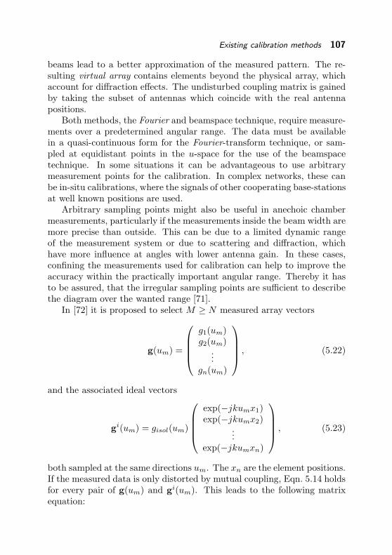
Existing calibration methods 107
beams lead to a better approximation of the measured pattern. The re-sulting virtual array contains elements beyond the physical array, whichaccount for diffraction effects. The undisturbed coupling matrix is gainedby taking the subset of antennas which coincide with the real antennapositions.
Both methods, the Fourier and beamspace technique, require measure-ments over a predetermined angular range. The data must be availablein a quasi-continuous form for the Fourier-transform technique, or sam-pled at equidistant points in the u-space for the use of the beamspacetechnique. In some situations it can be advantageous to use arbitrarymeasurement points for the calibration. In complex networks, these canbe in-situ calibrations, where the signals of other cooperating base-stationsat well known positions are used.
Arbitrary sampling points might also be useful in anechoic chambermeasurements, particularly if the measurements inside the beam width aremore precise than outside. This can be due to a limited dynamic rangeof the measurement system or due to scattering and diffraction, whichhave more influence at angles with lower antenna gain. In these cases,confining the measurements used for calibration can help to improve theaccuracy within the practically important angular range. Thereby it hasto be assured, that the irregular sampling points are sufficient to describethe diagram over the wanted range [71].
In [72] it is proposed to select M ≥ N measured array vectors
g(um) =
g1(um)g2(um)
...gn(um)
, (5.22)
and the associated ideal vectors
gi(um) = gisol(um)
exp(−jkumx1)exp(−jkumx2)
...exp(−jkumxn)
, (5.23)
both sampled at the same directions um. The xn are the element positions.If the measured data is only distorted by mutual coupling, Eqn. 5.14 holdsfor every pair of g(um) and gi(um). This leads to the following matrixequation:
108 Calibration
[g(u1) . . . g(um)
]= C ·
[gi(u1) . . . gi(um)
], (5.24)
orG = C ·Gi, (5.25)
respectively. For M = N the coupling matrix C can be calculated bysimple matrix inversion:
C = G(Gi
)−1(5.26)
For M > N the same approach leads to an overdetermined set of equa-tions. In [72], Eqn. 5.25 is rearranged to
GT(C−1
)T= GT
[c1 c2 . . . cn
]= GiT , (5.27)
with (. . .)T being the transposed matrix. This can be interpreted as Nleast squares problems
mincn
∥∥GT cn − gin
∥∥2
n = 1, 2, . . . , N, (5.28)
which can be solved numerically by QR-decomposition of GT (see [72] fordetails). The approach of numerical optimization of the coupling matrixcan be extended by additional virtual elements that account for possibleedge diffraction [73]. As a drawback, the matrix C then becomes rectan-gular and cannot be inverted and direct correction of the received signalsbecomes impossible. This constrains the range of possible applications ofthis method.
Last, the concept of the active element pattern [65] needs to be men-tioned: as long as there is a single-mode relationship between each elec-trical port state and the corresponding far-field pattern, all embeddedelement patterns can be stored numerically. This allows for arbitrary pat-terns of all elements, but the array factor model is not valid anymore.Hence, associated algorithms are computationally expensive. This can bepartly mitigated by employing this method just for the outer array ele-ments. The inner elements, which exhibit almost identical patterns, aretreated with the conventional array factor model [66].
Tab. 5.1 summarizes the advantages and drawbacks of the reviewedcalibration methods for the passive array.
5.2.3 Test-tone calibration
In most practical applications it is not possible to obtain reliable far-fielddata. The transfer function variations caused by the entire analog RF

Existing calibration methods 109
Table 5.1 Overview over methods for the calibration of passive antenna arrays.
method advantages drawbacks
from S-matrix [67] no anechoic chamber only passive arrayno difraction
deembedding difficultFourier technique active gain considered only well-behaved arrays
[67] no diffractionlimited to d > λ0/2
beamspace [69] removes diffraction diffraction not compensatedfewer samples only equidistant spacing
LS fitting [72] arbitrary points no diffraction2-D arrays
extended matrix [73] arbritrary points C not invertibleactive element [65] individual elements no C
no pattern constraints computational expensive
hardware, which often exhibit several dB and tenths of degrees of phaseshift, prevail the uncertainties resulting from mutual coupling.
As a commonly used pragmatic approach, a local calibration signal isemployed. This signal is distributed over a symmetrical network to ensurethat all fractions maintain identical phases and amplitudes. Directionalcouplers or switches are applied to inject the calibration tones at the inputof the downconverter chain. The resulting response to this set of identicalinput signals yields the appropriate values for compensation [74].
This straightforward procedure for the receive case poses difficulties intransmitting arrays. To avoid a superposition of all output signals it hasto be assured that only one signal reaches the test receiver. This usuallyis done by activating only one receiver at a time or by switching thecalibration network [75]. The basic principles are identical and, therefore,in the following it is not explicitly distinguished between transmitter andreceiver calibration.
Several methods are published that use the transmitted signals forjoint transmitter and receiver calibration to avoid additional hardware.Switching schemes are proposed for time-division duplex systems [76] andenhanced by frequency converters to calibrate frequency-division duplexsystems [77, 78]. All these methods require a multitude of switches andinterconnecting transmission lines, whose phase and gain equalities arecrucial for the obtainable precision.
An interesting method proposes to exploit the mutual coupling effectitself for the calibration of both, the mutual coupling and the active hard-ware [79]. As shown in Fig. 5.9, the calibration signal is generated by

110 Calibration
mutual coupling
element n element n+1cal signal
Fig. 5.9 Calibration using the mutual coupling [79]. The reciprocity of the mu-
tual coupling is used to determine the transmitter and receiver transfer functions
and the mutual coupling itself.
transmitter n. It is received by receiver n belonging to the same antennaelement. But, also, it is reaches the neighbored receiver n + 1 via mutualcoupling. The mutual coupling can be assumed to be reciprocal, givingthe same phase shift and attenuation to a signal travelling from elementn + 1 to element n. The gained information from these two situations canbe used to calculate all correction values, including the mutual couplingfactor between these two elements. It has to be considered that the result-ing coupling factor does not necessarily refer to the antenna phase center.Therefore, this method might not lead to the correct calibration matrixfor certain types of antennas or higher frequencies. In these cases it mightbe useful to introduce an appropriate deembedding distance, as neededfor the s-parameter method (compare 4.3.3). One severe drawback of thismethod is the requirement of simultaneous transmit and receive operation.
It has to be considered that the power levels at the transmitter andreceiver differ significantly. To ensure linear operation of the receiver and,hence, reliable values for calibration, a high isolation must be guaranteedbetween these components. This might be impossible to fulfill for compactand lightweight arrays.
All methods that use any kind of signal circulation of the own trans-mitted signal are referred to as ”self calibration”methods.
5.2.4 Hybrid methods
It is a reasonable assumption that, once an array is fabricated, the mu-tual coupling stays nearly constant, while the dominant changes resultfrom the active hardware. This motivates to combine a fixed compensa-tion of mutual coupling with a repeatedly determined correction of theactive hardware, which is gained by signal injection during normal oper-ation. The coupling matrix is either determined by field measurementsafter fabrication [80], or by electromagnetic simulation of the employedarray [81].

Existing calibration methods 111
C=1+S
(b)
R
(a)
phase
centerCAL
CAL
Fig. 5.10 Matrix representation of calibration: a) mutual coupling and unequal
transfer functions disturb the beam-forming process. b) these can be modelled
as a coupling matrix C and a diagonal gain matrix R.
5.2.5 Improved Hybrid Calibration
The hybrid methods proposed in literature assume a calibration model asdepicted in Fig. 5.10. A coupling matrix C and a gain matrix R associatedwith the active components are assumed, which are independent of eachother. Furthermore, it is demanded that C is determined by far-field mea-surements and R can be precisely gained from the local calibration signal.It is not considered that the reference network has a limited precision andthat possible mismatch might occur at the antenna and amplifier inter-faces, which lead to reflections. If a very precise calibration is needed,the hybrid calibration approach has to be extended to account for thisproblem.
All methods which base on the measured far-field automatically includethe complete transfer matrix RC, even including mismatch effects. Thiscan be exploited for a more precise calibration: if the disturbed active-gain matrix R is measured simultaneously or in short succession with thepattern measurements, it is possible to estimate the changes of RC. If tis the actual time and tcal is the time of far-field calibration, the diagonalentries of R are
rm(t) ≈ rm(tcal) ·rm(t)
rm(tcal), (5.29)
RC accordingly is
R(t) ·C(t) ≈
r1(t)/r1(tcal) 0. . .
0 rn(t)/rn(tcal)
·R(tcal) ·C(tcal)
(5.30)This procedure removes the deficiencies of the test-tone calibration net-work. However, it is still assumed that any mismatch at the antennainterface stays constant. Hence, the remaining uncertainties result from

112 Calibration
tk tt trkr r rk+1 k+11 1 N N
c ck1 c
a a a ab b b b1 1 k k k+1 k+1 N N
la
bl br
raN−1
all equal
Fig. 5.11 Underlying signal model for transmission line calibration.
a change of this matching and from the limited precision of the far-fieldmeasurements.
5.3 Transmission-line calibration method
As discussed above, the test-tone scheme requires a calibration signal thatis distributed via a symmetric power splitting network and injected intoeach receiver path using either switches or directional coupler. The neededsplitting network consumes a lot of space and poses a design challenge fortwo-dimensional, non-equally spaced or non-planar arrays.
Self-calibrating methods usually require a complex switching network[76–78] and demand very high internal isolation to permit simultaneoustransmit and receive operation.
The proposed method uses a single transmission line that links allbranches, whereby the estimation of the line segments themselves is partof the calibration. Therefore the hardware effort is noticeably reduced.
5.3.1 Description of method
For the derivation of the proposed method the signal model depicted inFig. 5.11 is assumed:
A ”bus-like”transmission line links all N transceiver branches, wherethe N-1 line segments are represented as complex transmission factors ck.The individual phase and amplitude responses of the transmitters andreceivers are modelled by the transmission constants tk and rk, wherebythe whole chain with frequency conversion to baseband is included. ak andbk are the complex transmitted and received signals. The transmitted andreceived signals of each transceiver are assumed to be coupled with thecalibration line at a single point. The calibration refers to this point andtherefore the electrical lengths from here to the antennas have to be equal.For this derivation it is assumed that
• the coupling is weak, no noteworthy signal travels from antenna k toadjacent receivers (e.g. loss >15 dB).
• no reflections of al, ar occur at the coupling points.

Transmission-line calibration method 113
tk trk rk+1 k+1
ck
a ak k+1
ak
tk rk tk+1
ak+1
rk+1
ck
ra
kb k+1b
k+1bkb
a l
Fig. 5.12 Signal flow for receiver calibration.
The influence of reflections and a possible practical realization will bediscussed later in sections 5.3.2 and 5.3.3.
Now the calibration signals al and ar, respectively, are successivelyapplied at both ends of the calibration line like shown in Fig. 5.12. Thetransfer function to each output k is
skl =bk
al= rk
k−1∏
m=1
cm (5.31)
and
skr =bk
ar= rk
N−1∏
m=k
cm. (5.32)
The transmission factor of each line segment is reciprocal and can becalculated by combining the equations 5.31 and 5.32 for k and k+1 andsolving for ck:
ck = ±
√s(k+1)l
skl·
skr
s(k+1)r. (5.33)
The sign of the above square root cannot be determined from the set ofequations, but it can be estimated if the approximate electrical length isknown:
cest = exp
(−j2π
f
c0lk,est
)(5.34)
If lest is not known either, it is possible to estimate it once from two closelyspaced (∆f < cπ
2l ) frequencies:

114 Calibration
lest = 6
(ck(f)
ck(f + ∆f)
)·
c0
2π∆f(5.35)
Once the values for ck are known, the relationship between two adjacentreceivers is given by
rk+1
rk=
1
ck·s(k+1)l
skl= ck
s(k+1)r
skr(5.36)
and thus all rk can be deduced with respect to one element the calibrationrefers to. The calculation of tk follows the same scheme, except thattransmitters and receivers are exchanged.
It has to be noted that no assumptions were made on al and ar, there-fore they can be generated in an arbitrary manner, e.g. by switching acalibration source to both inputs using lines of individual length.
5.3.2 Estimation of systematic error
To ascertain the hardware requirements, it is useful to estimate the sys-tematic errors introduced by the proposed calibration method. Theseerrors can be subdivided into two contributions:
• Variations in hardware, such as variations of the realized coupling be-tween calibration line and signal or variations of the electrical lengthbetween calibration point and antenna lead to errors in each individ-ual branch. These depend strongly on the particular implementationand can be estimated separately for each element.
• The proposed calibration method bases on an idealized signal modelthat is difficult to realize at microwave frequencies. Notably wavesare assumed that travel along the calibration line without reflections.Any practical realization will reflect a fraction of the signal and causea wave travelling backwards, disturbing the calibration values.
To gain some insight into the ability of this method the error caused bymismatches on the calibration line can be estimated. Again the receivingcase is regarded, while the transmitting case can be treated in the sameway and leads to the same results.
The basic ”calibration element”(see Fig. 5.13) can be approximated bythe following S-parameter matrix
S =
s11 1 a1 s22 aa a 0
, (5.37)
where ’a’ denotes the large coupling attenuation towards the receiver. Fora possible practical realization it is again referred to section 5.3.3. To sim-plify the calculation two reflection factors Γkl and Γkr are defined, that

Transmission-line calibration method 115
S1 2
3
rkΓk,rΓk,l
Fig. 5.13 Basic calibration element (receive mode)
tk t rk+1 k+1
a ak k+1
S11 (k+1),rΓ
kb k+1b
ck
rk
al
Fig. 5.14 Simplified error model
comprehend all superimposed reflection effects looking into the line struc-ture from receiver k to the left or right, respectively (compare Fig. 5.13).
Fig. 5.14 shows the used error model. Assuming that multiple reflec-tions between element k and k+1 can be neglected, the disturbed obser-vations s can be obtained for one pair of antennas:
s(k+1)l = s(k+1),l
(1 + Γ(k+1)r
)(5.38)
skl = sk,l
(1 + c2
ks11 + c2kΓ(k+1)r
)(5.39)
skr and s(k+1)r are calculated accordingly.Equations (5.33) and (5.36) can be combined to obtain the transmis-
sion ratio of two neighbored elements
rk+1
rk= ±
√s(k+1)l
skl
s(k+1)r
skr. (5.40)
Inserting the disturbed observations s leads to the disturbed ratio
rk+1
rk= ±
rk+1
rk
√(1 + Γ(k+1)r) · (1 + c2
ks22 + c2kΓkl)
(1 + c2ks11 + c2
kΓ(k+1)r) · (1 + Γkl). (5.41)
If all double reflections s11s22 ≈ 0 and Γmsnn ≈ 0 are neglected, thiscan be simplified to

116 Calibration
rk+1
rk≈ ±
rk+1
rk
√1 + c2
ks22 + c2kΓkl + Γ(k+1)r
1 + c2ks11 + c2
kΓ(k+1)r + Γkr︸ ︷︷ ︸
ε
. (5.42)
Under the assumption that all reflections are small, Γ 1, the result-ing error ε can be linearized to
ε ≈ Γkl ·∂
∂Γklε + Γ(k+1)r ·
∂
∂Γ(k+1)rε. (5.43)
Assuming that the ”calibration element”is symmetric and s11 = s22
this results in the following simplified expression:
rk+1
rk≈ ±
rk+1
rk
(1 +
1
2
(c2k − 1
) (Γkl − Γ(k+1)r
)). (5.44)
According to this expression, the systematic calibration error dependson the electrical length of the calibration line segments and the differencebetween the reflection factors Γkl and Γ(k+1)r seen from the consideredreceiver pair into the left and right transmission line structure.
With periodic spacing one has to keep in mind that for certain ck allsmall reflections might add up to a strong reflection Γ, so that this Braggcondition should be avoided.
For illustration an ideal six-element periodic structure with a singleelement return loss of −20 dB is simulated. The reflection coefficients Γ2l
and Γ3r are shown in Fig. 5.15.For 5 GHz, where the segment length lk is λ/2, the return loss of the
structure gets worse than −10 dB as an effect of the periodic arrangement.
For the same structure the systematic calibration error r3/r2
r3/r2of this
pair of elements is calculated using both, the complete algorithm and theapproximated expression in Eqn. (5.44). The results are compared inFig. 5.16.
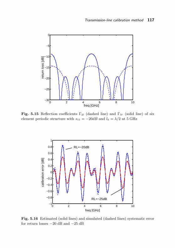
Transmission-line calibration method 117
0 2 4 6 8 10−30
−25
−20
−15
−10
−5
0
freq [GHz]
retu
rn lo
ss [d
B]
Fig. 5.15 Reflection coefficients Γ2l (dashed line) and Γ3r (solid line) of six
element periodic structure with s11 = −20dB and lk = λ/2 at 5 GHz
0 2 4 6 8 10−1
−0.8
−0.6
−0.4
−0.2
0
0.2
0.4
0.6
0.8
1
freq [GHz]
calib
ratio
n er
ror
[dB
]
RL=−20dB
RL=−25dB
Fig. 5.16 Estimated (solid lines) and simulated (dashed lines) systematic error
for return losses −20 dB and −25 dB

118 Calibration
For return losses s11=s22=−20dB and −25 dB the simulated and ap-proximated errors agree well, except a range around 5 GHz where theassumption of a small reflection Γ3r 1 is violated due to the fulfilledBragg condition. The maximum error stays below 0.9 dB for s11 = −20dBand below 0.5 dB for s11 = −25dB. Return losses of such magnitudes canbe achieved with a transmission line structure.
It has to be noted that in the analysis above it never was assumed that|ck| = 1 for the transmission line segments. Introducing attenuation heremight help to improve the matching and weaken far end reflections.
5.3.3 GaAs transmit/receive-switch with calibration ability
The hardware necessary for this calibration method was integrated to-gether with a transmit/receive-switch for an active antenna array system.The simplified schematic is shown in Fig. 5.17: the needed coupling isachieved by a capacitor with C=150 fF. This value was set to obtain atransfer function |sRX,cal| of −15 dB at 6 GHz which leads to an antenna-to-antenna isolation of −30 dB.
This capacitor and the bond-pad capacitances form a low-pass trans-mission line structure together with the inductances of the bond-wires andon-chip lines. T-structure FET switches are used to switch between trans-mit and receive mode, so that the open switch presents a high impedanceat the combination point. As the calibration is done with respect to this
couplingcapacitor
inductanceparasitic
bondwires
Rx
Tx−switch
CAL CAL
monolithiccircuit
antenna
Tx
Rx−switch
Fig. 5.17 Schematic of Tx/Rx-switch with calibration capability

Transmission-line calibration method 119
point the switches are designed according to their individual demand fortransmit/ receive operation. The circuit was fabricated using a 0.6 µmGaAs MESFET process.
5.3.4 Experimental Results
To verify the proposed concept a test setup was built, employing four ofthe transmit/receive-switches described above. Fig. 5.18 shows a pictureof the circuit. The calibration ports are linked by a single transmissionline.
The lines connecting the antenna ports are kept at equal lengths, whilethe lines connecting transmitter and receiver have individual distances.The necessary transfer functions from the left and right end of the cali-bration line to each transmitter/receiver were measured using a networkanalyzer. The individual transfer functions to the different antennas werealso determined for comparison.
Fig. 5.19 shows the estimated phase 6 ck of the three calibration lineelements over a frequency range up to 10 GHz. The deviation from theideal progression at around 5 GHz is due to the mounting pad of thechip. Measurements of the empty structure without chip show a parasiticcoupling path at this frequency. For operation at this frequency one wouldneed to choose a different layout.
! ! ! !! ! ! !! ! ! !! ! ! !! ! ! !! ! ! !! ! ! !
" " "" " "" " "" " "" " "" " "" " "" " "" " "" " "" " "
# # ## # ## # ## # ## # ## # ## # ## # ## # ## # ## # #
$ $ $ $ $ $ $ $$ $ $ $ $ $ $ $$ $ $ $ $ $ $ $$ $ $ $ $ $ $ $$ $ $ $ $ $ $ $$ $ $ $ $ $ $ $$ $ $ $ $ $ $ $$ $ $ $ $ $ $ $$ $ $ $ $ $ $ $
% % % % % % % %% % % % % % % %% % % % % % % %% % % % % % % %% % % % % % % %% % % % % % % %% % % % % % % %% % % % % % % %% % % % % % % %
& & & & & & & & & & & & &' ' ' ' ' ' ' ' ' ' ' ' '( ( ( ( ( ( ( ( ( ( ( ( ( ( ( ( ( (( ( ( ( ( ( ( ( ( ( ( ( ( ( ( ( ( (( ( ( ( ( ( ( ( ( ( ( ( ( ( ( ( ( (( ( ( ( ( ( ( ( ( ( ( ( ( ( ( ( ( (
) ) ) ) ) ) ) ) ) ) ) ) ) ) ) ) ) )) ) ) ) ) ) ) ) ) ) ) ) ) ) ) ) ) )) ) ) ) ) ) ) ) ) ) ) ) ) ) ) ) ) )) ) ) ) ) ) ) ) ) ) ) ) ) ) ) ) ) )
calibration
line
antenna
ports
Tx/Rx−
switches
transmit
ports
ports
receive
Fig. 5.18 Test substrate (size ∼50×50 mm2)

120 Calibration
0 2 4 6 8 10
−150
−100
−50
0
50
100
150
freq [GHz]
phas
e [d
eg]
Fig. 5.19 Estimated transmission phase of calibration line segments
From the reference measurements (antenna to receive ports) the re-sulting array factor for a unity distribution is calculated and depicted inFig. 5.20. The main beam, side lobes and zero positions are significantlyshifted compared to the theoretical pattern. The calibrated outputs areobtained by simply multiplying the inverse of the estimate:
bk,cal = r−1k · bk (5.45)
The resulting pattern is also depicted in Fig. 5.20. Except slightly changedside-lobes and finite zero depths it resembles the ideal pattern. For com-parison, also the residual side-lobe level is plotted to demonstrate thestatistically expected zero depth.
To quantitatively characterize the array calibration, the residual side-lobe level and the pattern zeros at 0 and 60 are calculated over a broadfrequency range. Fig. 5.21 shows the achieved results after calibration.Apart from f=5 GHz, where unwanted coupling occurs, the notch stayswell below −20 dB up to 7 GHz.
This demonstrates that the proposed method can replace the space-consuming symmetrical divider network, usually used for array calibration.The linking transmission line is part of the calibration itself and, there-fore, does not follow any layout constraints. In applications where theobtained precision is sufficient, it can be used to calibrate antenna arraysof arbitrary arrangement. The method is inherently broadband and easilycompatible with monolithic front ends to form compact active arrays.

Transmission-line calibration method 121
0 45 90 135 180 225 270 315 360−35
−30
−25
−20
−15
−10
−5
0
5
10
15
angle [deg.]
arra
y fa
ctor
[dB
]
Fig. 5.20 Uncalibrated (line with crosses) and calibrated array factor (solid
line) (receiving mode) at 4 GHz compared to the ideal value (dashed line). The
circles indicate the residual side-lobe level calculated from the measurements.
0 2 4 6 8 10−50
−45
−40
−35
−30
−25
−20
−15
−10
freq [GHz]
zero
dep
th [d
B]
Fig. 5.21 Zero depth after calibration (receiving mode) for the null at 60 (solid
line) and at 0 (dashed line) and residual side-lobe level (circles).

122 Calibration
5.4 Dynamic transmitter calibration
So far, it was always assumed that the hardware introduces slowly varyingrandom changes. It is demanded that the individual transfer functionsstay constant during a typical data transmission. This neglects switchingof the power amplifiers in time-domain access schemes.
As already pointed out in chapter 3.5, switching the power transistorsleads to strong thermal changes in the semiconductor devices, exceed-ing those caused by fluctuations of the ambient temperature by orders ofmagnitude. In contrast to environmental influences, these variations areof deterministic nature and can be expected to be partly correlated.
One way to go around this question is to bias the power amplifiers con-stantly, but in practice a shutdown during periods of inactivity is very at-tractive to save battery power and fulfill the strict emission limits. There-fore, the correlation of switched power amplifiers with respect to theirapplication in antenna arrays is investigated in the following. This allowsto derive guidelines how and when such a system needs to be calibrated.
5.4.1 Instantaneous error
For the time-variant transmitting case, the transmitted vector wTX is
wTX(t) = C(t) · w = C ·(C−1w(t)
), (5.46)
where w is the ideal vector and w and C are the preconditioned vectorand the estimated correction matrix, respectively. In the following theantenna uncertainties are excluded and it is assumed, that a couplingmatrix estimation
C = C(t0) (5.47)
can be found, which perfectly compensates the coupling at time t0. Theinstantaneous array error at all other times t 6= t0 then is
e(t) = minc
wwc ·wTX(t) − w(t)ww, (5.48)
or
e(t) = minc
www(c ·C(t)C−1(t0) − 1
)w(t)
www . (5.49)
This error measure, previously discussed in section 5.1.4, is used to includeonly those errors that lead to a deformation of the wanted antenna pattern.In the case of jointly switched power amplifiers it is expected that thegain and phase changes are partly correlated. These common changes areaccounted for with the complex scalar factor c.

Dynamic transmitter calibration 123
and
sig
nal sto
rage
PA attenuator
26dB converterdown−
PAswitch
LO6.65 GHz
5.2GHz
RF
multi−
channel re
ceiv
er
Fig. 5.22 Experimental setup to determine gain and phase correlation of si-
multaneously switched power amplifiers.
For universality a uniform distribution with |wn| = 1 is chosen and theaverage error power
|enorm|2 =1
Nee∗ (5.50)
referred to a single element is used in the following.
5.4.2 Power amplifier
To conduct the transmit calibration experiment, four of the GaAs poweramplifiers presented in chapter 3.5 are used. As described there, theseamplifiers deliver 19 dBm output power at the 1 dB-compression point.This is a comparably low value and takes advantage of the inherent powersplitting and additional gain that occur in array antennas.
It is recalled that two thermal time-constants were found, one of 1.6 msand a second of 2200 ms. It was observed that the gain decreases withraising temperature, which is a typical behavior.
5.4.3 Array calibration
To evaluate the impact of the thermal changes on the system behavior, itis necessary to drive all amplifiers simultaneously and regard the changesand their correlation behavior during a typical burst. For this purpose thesetup shown in Fig. 5.22 is used:
The four power amplifiers are driven by the same frequency source andswitched simultaneously. A smart antenna test-bed, consisting of MMICdownconverters (see section 3.3.3) and a multichannel receiver, is used torecord the output. Attenuators reduce the effect of possible mismatchand, at the same time, ensure a linear operation of the receiver.

124 Calibration
on
off
time
7Tburst
Tburst
2Tburst
referencepulse
Fig. 5.23 Used switching scheme: periodic frame structure with variable num-
ber of bursts. The calibration is acquired at the first measured frame and kept
constant afterwards.
Fig. 5.23 illustrates the used switching scheme: a frame structure withseven time slots is assumed, each time slot 250 µs long. The frame patternis repeated periodically. According to the HiperLAN standard, the actualtransmit pulse can be a multiple of the 250 µs slot length. Here, this isemulated with a varying duty cycle from 1/7 to 7/7, occupying one orseveral time slots.
The experiment starts with a 250 µs pulse. A period of around 120 msis recorded, covering 71 pulses. The complex calibration values cn are cal-culated from average gain and phase of the first pulse recorded. Fig. 5.24shows the graph of pulses no. 70 and 71 after calibration. Although theamplifiers have been turned off several times and the isolation during theoff-period varies significantly, the calibrated gain agrees very well withthe reference level. The observed gain variation between start and end ofthe pulse is less than 0.2 dB. The initial overshooting is due to the fastswitching. In a real system this would cause unwanted spurious emission.A controlled ramp-up would be used to avoid this transient.
Maintaining the same calibration values, now the duty cycle again isvaried by increasing the pulse length. As shown in Fig. 5.25, a decreasinggain is observed for all channels, but the changes are no longer identicalas in the previous case.
The different variations result in an increased calibration error. How-ever, the element error power |e|2 averaged over all bursts stays less than−33 dB, which is fairly low. This corresponds to a residual side-lobe levelof less than −39 dB in a four element array.
Fig. 5.26 shows the progression of the instantaneous error power dur-ing one burst. For both curves, at the initial duty cycle of 1/7 and the

Dynamic transmitter calibration 125
0 500 1000 1500 2000 2500 3000 3500−35
−30
−25
−20
−15
−10
−5
0
5
time [usec]
rel.
gain
[dB
]
pulse 70 pulse 71
+0.1
−0.1
Fig. 5.24 Calibrated gain of all four channels, 120 ms after calibration, constant
duty cycle 1/7. The inset shows the gain transients during the last pulse. All
four channels are almost identical.
increased cycle of 6/7, it can be seen that the error power stays almost con-stant for the duration of the whole pulse. This demonstrates that a fixedset of values cn is sufficient for calibration over a typical burst duration.No time-dependent calibration is needed.
It can be concluded that all gain and phase changes taking place inthe range of the first thermal time-constant of 1.6 ms are well correlated.The changes associated with the second time constant of 2200 ms showthe same tendency, but are individually different for each amplifier.

126 Calibration
1/7 2/7 3/7 4/7 5/7 6/7 7/7−1
−0.5
0
0.5
duty cycle [1]
rel.
gain
[dB
]
−30
−35
−40
−45
erro
r po
wer
[dB
]
1 2
3 4
Fig. 5.25 Gain variation of all four channels and calibration error for different
duty cycles, calibration on duty cycle 1/7.
0 500 1000 1500 2000−90
−80
−70
−60
−50
−40
−30
−20
−10
0
10
time [usec]
erro
r po
wer
[dB
]
duty cycle 1/7
duty cycle 6/7
Fig. 5.26 Instantaneous element error during pulse 70 for duty cycles 1/7
(solid) and 6/7 (dashed), calibrated on duty cycle 1/7.

Conclusions 127
heat
sourceRth,1
τ1
Rth,2
τ2
on−chip
off−chip
Fig. 5.27 Thermal model derived from the measured temperature transients.
It is assumed that the second time-constant is determined by the off-chip envi-
ronment and, therefore, can differ from amplifier to amplifier in an array.
One possible explanation of this behavior can be derived from the ther-mal model depicted in Fig. 5.27. It can be assumed that the small firsttime-constant is basically defined by the heat capacity of the power deviceand the thermal substrate resistance. Both can be attributed to physicalproperties of the chip. As monolithically integrated circuits are used, thesevalues should be virtually identical for all amplifiers. The second time-constant, in contrast, can be expected to be given by the chip mounting,the further substrate around and the final thermal resistance to the en-vironment. All these factors depend on the position of the chip on thetesting substrate and the assembling process. This will result in differentthermal resistances Rth,2 and, hence, different junction temperatures andgains of the devices.
5.5 Conclusions
In this chapter, various methods for array calibration are reviewed. Fora complete calibration, far-field sources are necessary to include all mu-tual coupling and diffraction effects. A local test-tone calibration can beused to compensate for the variations of the active circuitry. Only themutual coupling self-calibrating technique is suitable to determine thesevariations and the coupling matrix of the array. This method requiressimultaneous transmit and receive operation and, therefore, is difficult toapply to compact systems due to the high isolation needed.
A new calibration scheme is proposed that employs a local coupling be-tween all branches provided by a weakly coupled transmission line, whichlinks all elements. The determination of the transmission factors of theline segments is part of the calibration process itself. This allows an arbi-

128 Calibration
trary arrangement and replaces the previously needed precise and bulkydivider network.
To derive guidelines for necessary calibration intervals, the dynamicbehavior of switched power amplifiers is studied with respect to applicationin transmit antenna arrays. On monolithically integrated power amplifierstwo thermal time-constants are experimentally found. A a typical burstup to a duration of milliseconds can be calibrated using a single set ofcorrection values. If the duty cycle stays constant, the obtained valuescan be reused for several pulses. For a changed duty cycle the variationsare less correlated and a slight pattern variation occurs.
6
Active antenna arrays
In this chapter, the construction of active antenna arrays is discussed.The monolithically integrated frontend presented in chapter 3 is used toyield compact and robust arrays. For a four element linear array, thedifferent calibration methods are evaluated to gain information about theobtainable precision.
The antenna front-end is integrated into a complete multiple-antennatest-bed, including conversion to digital baseband and storage of the re-ceived signal. Amplitude and phase stability as well as the noise perfor-mance of this system are studied with respect to a practical applicationin a communication system.
Last, it is demonstrated that the monolithically integrated RF fron-tends together with the transmission line calibration technique enable thesimple fabrication of conformal arrays.
6.1 Linear array
6.1.1 Design
In chapter 2.4 the architecture of a multiple-antenna test-bed is discussed.The active antenna array described here is conceived as the RF front-endto this system. The function can be explained from the block diagramdepicted in Fig. 6.1: the four antenna signals are processed independentlyby four receiver branches. These consist of monolithically integrated low-noise amplifiers and downconverters, both documented in chapter 3. Im-age rejection is achieved by a coupled-line bandpass filter in microstriptechnology. The measured pass-band attenuation of this filter is less than1 dB, the entire image band is suppressed by more than 50 dB. At the costof a reduced image rejection, this circuit combination could be replacedby the much smaller integrated receiver (see section 3.4), which was notavailable at the time of construction of this array.
The LO signal is symmetrically distributed to all downconverters bycascaded 2:1 Wilkinson power-dividers. The same signal is also used for
130 Active antenna arrays
LO
CAL IF1 IF2 IF3 IF4
down−converter
directional
coupler
coupled
line
filter
LNA
patch antennas
atte
nu
ato
r
Fig. 6.1 System block diagram of the active antenna front-end. Dashed lines
indicate monolithically integrated components.
the up-conversion of a signal used for calibration.The difficulty in this signal upconversion is the spectrally close spacing
of the resulting mixing products and the LO signal. To drive the mixer,a comparably high power of around 10 dBm is needed. Even if a mixerwith a good LO to RF isolation of 40 dB or better is used, the leakingsignal exhibits a significant power. The proximity of the wanted andunwanted components makes filtering difficult. In this case the possibleRF frequencies reach up to 5.875 GHz and the LO range starts at 6.6 GHz,resulting in a sharp transition from pass-band to stop-band.
To mitigate this problem, a high power of the calibration signal of up to0 dBm is chosen, which is the highest possible level for linear operation ofthe mixer. This guarantees the maximal output power level compared tothe LO spurious. Then, an attenuator is used to attenuate both, the signalof interest and the unwanted spurious. The image frequency is removedby six-section coupled-line filter, identical to those used in the receiverbranches. After the signal is symmetrically divided, it is coupled to thereceiver branches using directional couplers. Considering the conversionloss of 8 dB, the 15 dB attenuation, the signal distribution (≥ 6 dB), andthe coupling attenuation of 15 dB, the power of the calibration signalat the input of each branch is significantly below the input compressionpoint. This is important to avoid calibration errors due to gain and phasechanges caused by the compression behavior of the receivers.
The complete circuit is printed on a Duroid 6010 microstrip substrate

Linear array 131
patc
h
slo
t
image
filter
calib
ration
netw
ork
DC
-supply
LN
A
dow
n-
convert
er
IF 1
IF 2
IF 3
IF 4
MIX
LO
CA
L
CA
Lm
ixer
attenuato
r
mechanic
al
support
Fig. 6.2 Layout of the four element linear antenna array seen from the circuit
side. Substrate size is 150 ×117 mm.
(εr = 10.2, h = 635 µm) with the aperture-coupled patch antennas (com-pare chapter 4) mounted on the backside. Fig. 6.2 shows the final layout.
It was taken care that all signal lines are well separated in order toavoid unintended cross-talk. The calibration network, whose precision isimportant, avoids any crossings with other signal lines. The number ofdifferent signals, however, requires certain crossings of transmission lines.In these cases the line carrying the signal with the lower frequency isinterrupted and bridged with a bondwire. This keeps all transfer functionsas close to each other as possible.

132 Active antenna arrays
Fig. 6.3 Picture of the four element linear array. On top the four antenna
substrates with the slanted patch antennas are visible.
The antennas are equally spaced with a distance of 27.3 mm fromcenter to center. This corresponds to half of the free-space wavelengthλ0 at the center frequency of 5.5 GHz. A 45-slanted linear polarizationis chosen for this prototype. Each antenna employs two coupling slotsfor both perpendicular polarizations, out of which only one is used. Thesecond antenna port is terminated with a 50 Ω resistor.
The large substrate, which measures 150 × 117 mm, is mechanicallysupported at several points to ensure mechanical stability. As the mostcritical part, the fixture of the connectors was reinforced. The mechanicalrobustness is of great importance for the electrical performance; particu-larly it removes an important source for amplitude and phase variations.Fig. 6.3 shows a picture of the manufactured array.
6.1.2 Experimental results
After manufacturing, the active antenna array was characterized insidean anechoic chamber. Thereby, it had to be considered that this arrayincludes a frequency conversion process. A reference mixer was used tocalibrate the measurement system; the yielded results then were correctedby the previously measured conversion loss of this mixer. Fig. 6.4 showsthe total absolute gain of all four measured channels. This includes theconversion gain of the receiver, but also the gain of the passive antennastructure. From the measurement of a single antenna alone, a passive
Linear array 133
5 5.2 5.4 5.6 5.8 625
27
29
31
33
35
freq [GHz]
tota
l gai
n [d
Bi]
ch1ch2ch3ch4
Fig. 6.4 Measured gain of all four individual channels. This total gain includes
the passive antenna gain compared to an isotropic radiator and the additional
active conversion gain.
antenna gain of around 5.5 dB can be assumed. It is found that all fourchannels show similar gains. The total gain is around 30 dB, correspondingto approximately 25 dB active conversion gain.
Subsequently, the array was rotated to measure the directional pat-terns. The definition of angles is illustrated in Fig. 6.5. A change of ele-vation corresponds to the angle θ, the main-beam of the elements pointsat θ = 90. φ describes the azimuthal rotation of the array. This is theplane in which the beam can be steered by changing the element weights.φ = 0 is the main-beam direction of the antenna elements.
Fig. 6.6 shows the directional pattern for different elevations 0 ≤ θ ≤180. All element patterns are similar. For comparison, the pattern of asingle element is simulated and depicted. At 5.5 GHz an active gain of27 dB is assumed. For a certain range around the main beam θ = 90 agood agreement is found. For radiation almost parallel to the substratesurface the patterns differ. This can be explained by the effect of thefinite substrate, which is not included in the simulation. Also cables andconnectors are present that affect the pattern measurements.
The patterns measured for azimuthal rotation is significantly different:as seen in Fig. 6.7, all patterns exhibit a strong superimposed gain ripple,which can not be found on the simulated curve of the single element.
134 Active antenna arrays
z
x
yθ
ϕ τ
Fig. 6.5 Definition of axes and angles: the main direction of radiation is along
the x-axis at (θ = 90, φ = 0). The angle θ between main direction and the
z-axis is also referred to as elevation. φ is the azimuthal rotation around the
z-axis. The array can be steered in the φ-plane.
Furthermore, the limited size of the antenna elements does not explain gainchanges occurring with this high spatial frequency. Thus, it is suspectedthat these pattern deformations are a consequence of mutual couplingamong the individual antennas. This coupling and the possible calibrationare further discussed in the following section 6.1.3.
The linearity of the antenna front-end is characterized outside of ananechoic environment. Using a transmit antenna at a very close distanceto the array, high input power levels can be easily reached and possiblemulti-path propagations can be neglected. This allows both, to perform atwo-tone test and to drive the receiver into compression. The attenuationof the radio link is not known, therefore, the compression point and IP3
are determined as output referred values. From the approximate conver-sion gain of the active circuit the intercept and compression points at theantenna/ amplifier interface can be estimated. For all channels compres-sion points of approximately −25 dBm and third-order intercept points of−16 dBm are found this way.
The noise figures can not be measured directly by ENR-measurements,they have to be calculated from the known gain and the absolute noisepower at the output. This method contains several uncertainties, such asthe estimated active gain. The yielded results exhibit measurement errorsin the same order of magnitude as the noise figures themselves. Here, it isassumed that the noise figures are similar to the values measured on thereceivers alone, which are approximately 3.5 dB.
The DC power consumption of the complete front-end is 230 mA from a3 V supply. All figures-of-merit of this linear active array are summarizedin Tab. 6.1.

Linear array 135
15
20
25
30
35
60
300
180150
120
90
Fig. 6.6 Measured (solid lines) and simulated (dashed line) elevation patterns
at 5.5 GHz. Total gain in dBi. The simulated pattern assumes an active gain
of 27 dB.
15
20
25
30
35
60
300
−30
−60
−90 90
Fig. 6.7 Measured (solid lines) and simulated (dashed line) azimuthal pattern
at 5.5 GHz. The simulated pattern again assumes additional 27 dB active gain.
136 Active antenna arrays
Table 6.1 Summary of front-end characteristics
Parameter Value
layout linear 4 × 1polarization 45-slantedpassive gain ≈5.5 dBiactive gain 24.5 dBP1dB −25.1 dBmIIP3 −16.3 dBmDC-supply 3 V, 230 mANF ≈3.5 dB
6.1.3 Calibration
As seen above, a significant mutual coupling between the antenna elementsis present, which leads to a deformation of the azimuthal element patterns.In the previous chapter several methods were outlined, how to determineand compensate this coupling. Thereby, it was assumed that only oneradiation mode is linked to each individual antenna element, which canbe fully described by a corresponding port voltage. Furthermore, it wassupposed, that the isolated element pattern is not changed by bringing theantenna into the vicinity of others (assumption of well-behaved antennas).To verify if the real array fulfils these conditions, the different calibrationmethods are applied to the measured far-field patterns.
Fig. 6.8 shows the ideal array pattern for a uniform distribution. Itis gained by superposition of simulated isolated-element patterns. Thebeam is tilted 30 to avoid a symmetrical situation, which could partlycover the effect of mutual coupling. The measured pattern is depictedin the same Fig. 6.8. The side-lobe and notch positions differ from theideal angles. If the Fourier transformation technique is used to calculatethe coupling matrix C and to correct the received signals, a significantlyimproved pattern is obtained. Within a range of ±60 off broadside, themeasured pattern agrees well with the ideal one. An effective zero depthof more than 24 dB is obtained.
To evaluate if radiation from the substrate edges has some effect onthe pattern, the beamspace technique is applied to the same measure-ment data. Fig. 6.9 shows the calculated virtual array illuminations thatsynthesize the four individual element patterns. As expected, the maincontribution of each element is found at its physical location. The re-spective neighbor elements show a parasitic excitation of −17 to −20 dBrelative to the particular element. Apart from these values, which roughly

Linear array 137
−80 −60 −40 −20 0 20 40 60 80−40
−35
−30
−25
−20
−15
−10
−5
0
5
10
phi [deg]
dire
ctiv
ity [d
B]
Fig. 6.8 Uncalibrated (solid line with circles), calibrated (solid line with
crosses) and ideal (dashed line) array pattern for a uniform distribution tilted
to 30. This calibration bases on the Fourier-transform technique [67].
2 4 6 8 10 12 14 16 18 20−40
−35
−30
−25
−20
−15
−10
−5
0
5
10
element number
exci
tatio
n [d
B]
physicalarray
Fig. 6.9 Relative excitation of the 20-element virtual array gained using the
beamspace-technique [69]. Elements 9–12 coincide with the physical array. The
corresponding illumination values are the estimated entries of the coupling ma-
trix C.

138 Active antenna arrays
coincide with the coupling matrix given by the Fourier transformationtechnique, no other significant contributions beyond the physical array arefound. Contrary to the waveguide array in [69], no noticeable radiationfrom the substrate edges is present in this array.
To compare the performance of the different calibration methods dis-cussed in chapter 5.2.1, it is useful to employ a suitable error measurerather than looking at the array diagram for a fixed steering angle. InFig. 6.10, the residual error according to chapter 5.1.4 is calculated for auniform distribution steered from −90 to +90. Within a range of −60
to 60, all methods show a significantly lower error power compared to theuncalibrated results. For angles outside, the error power remains high; noimprovement is obtained by the calibration. Also it is noteworthy, that theFourier transformation technique and the beamspace method yield similarresults.
In contrast to the other methods, the least-squares fitting method offersthe flexibility to select arbitrary sampling points. It is found that, concen-trating these points to a small angular range, a very low error power can beachieved within this limited region. If the sampling points are spread morewidely, the mean error increases. For sampling points uniformly spaced in
−90 −60 −30 0 30 60 90−30
−25
−20
−15
−10
−5
0
phi [deg]
erro
r po
wer
[dB
]
Fig. 6.10 Calculated residual error after calibration (compare chapter 5.1.4):
uncalibrated (dashed line), Fourier transform technique (solid line), beamspace
technique (solid line with circles) and least-squares fit (solid line with crosses).
For the last two methods, the symbols are placed on the used sampling points.

Gain and phase stability 139
−15
−10
−5
0
60
300
−30
−60
−90 90
Fig. 6.11 Azimuthal calibrated element pattern (solid lines) compared to the
simulated isolated element pattern (dashed line). Least-squares fit equally
spaced in u from sin(−40) to sin(40) is used for calibration.
u between −40 and 40, the calibration results are slightly better thangiven by the other methods.
Using the gained calibration matrix, it is possible to correct the singleelement pattern. The results are shown in Fig. 6.11. For a certain anglearound the main beam direction, the corrected pattern agree well with theisolated element pattern.
It can be concluded that the behavior of this realized active array canbe approximated by the ideal uncoupled sensor model. For the relevantrange of the antenna beam width a good agreement can be obtained.Outside of this range the element pattern differ from the ideal patternand can not be corrected by calibration. Concentrating the calibration onthis reasonable range, the residual error within this region can be furtherminimized.
6.2 Gain and phase stability
To guarantee the correct spatial signal processing, the different processingpaths need to have stable phase and amplitude responses with respect toeach other. This aspect is investigated on the complete smart antennatest-bed described in chapter 2.4. This system allows to simultaneouslyreceive all four channels and to store the results. A microwave signalgenerator is used to generate a constant sinusoidal signal that is connected

140 Active antenna arrays
to the calibration port of the active antenna front-end. The system is leftrunning for three days in a normal office environment.
The recorded results are normalized on the first sample. The observedgain and phase changes are depicted in Fig. 6.12 and Fig. 6.13, respec-tively. The phases are referred to the phase of the first channel, becausethe calibration signal source and the local receiver oscillators are not syn-chronized, resulting in random absolute phases.
It is observed, that the gain and phase changes of ±0.1 dB and ±1,respectively, are very small. All channels show a similar progression, whichfurther reduces the effect on the spatial processing. To demonstrate this,the calculated zero depth and residual side-lobe level are shown in Fig. 6.14
The maximum values of −38 dB for the residual side-lobe level and46 dB for the zero depth are very low, if it is considered that during threedays no new calibration is performed.
From the gain variation in Fig. 6.12 and the zero depth in Fig. 6.14, par-ticularly, a daily cycle can be observed. This regularity can be explainedby a temperature dependence of the analog signal processing section. Forverification, the active antenna front-end is placed inside a climatic ex-posure cabinet, which generates abrupt temperature changes. Fig. 6.15shows the gain changes that result from a sudden temperature changefrom 0 C to 25 C. The gain variations are more than 1 dB and also thedifferences between the channels become significant.
Obviously, the gain and phase changes are mainly caused by temper-ature variations.

Gain and phase stability 141
0 10 20 30 40 50 60 70−0.2
−0.1
0
0.1
0.2
time [hours]
gain
var
iatio
n [d
B]
Fig. 6.12 Measured gain variation over three days of all four channels. The
values include the complete test-bed and were recorded in a normal office envi-
ronment.
0 10 20 30 40 50 60 70−2
−1
0
1
time [hours]
phas
e va
riatio
n [d
eg]
Fig. 6.13 Test-bed phase variations over three days. Three channels referred
to the first channel.

142 Active antenna arrays
0 10 20 30 40 50 60 70−70
−60
−50
−40
−30
time [hours]
zero
dep
th [d
B]
Fig. 6.14 Calculated null depth (solid line) and residual side-lobe level (dashed
line) over three days.
0 10 20 30 40 50 60−1.5
−1
−0.5
0
0.5
time [min]
ampl
itude
var
iatio
n [d
B r
el.]
1
2
3
4
Fig. 6.15 Gain variation of the four front-end channels for a forced temperature
step from 0 C to 25 C.

Noise correlation 143
6.3 Noise correlation
As discussed in chapter 2.3, the spatial processing typically requires thatthe amplitude noise contributed by the receivers is uncorrelated. Thephase noise, in contrast, should be dominated by the phase noise of theLO. The contribution of the individual branches to the phase noise has tobe prevented to avoid any zero leakage.
6.3.1 Amplitude noise correlation
To characterize the noise added by the system, the receiver is operated ina shielded environment with no signals present. To study the influence ofthe different system blocks (compare Fig. 2.13), the system without thefrontend is examined first.
Fig. 6.16 shows a typical output noise-spectrum when the analog fron-tend is removed. The observed spurious level is common in communicationsystems. It originates from the unwanted injection of the switching andclock noise emitted from the digital circuits into the analog hardware.Usually it can be tolerated, because its contribution to the total noisepower is low. To observe the noise correlation, the angular dependentmean noise power
Pnoise(θ) =1
T
T∑
t=1
( N∑
n=1
an(t)e−j2π n∆λ
sin θ)2
(6.1)
is calculated and depicted in Fig. 6.17, where ∆/λ is 0.5, T the number oftime samples and θ the angle into which the array is steered. Compared
−100 −50 0 50 100−150
−140
−130
−120
−110
−100
−90
−80
freq [kHz]
[dB
FS
]
Fig. 6.16 Noise spectrum of digital downconverter (DDC) with spurious, rela-
tive to full scale excitation (dBFS).

144 Active antenna arrays
10
20
30
30
210
60
240
90
270
120
300
150
330
180 0
DDC only
system
Fig. 6.17 Directional pattern of the digital part and the complete system (solid
lines) compared to the not coherently added noise levels (dashed lines).
to the theoretical pattern without correlation
Pn,uncorr =1
T
T∑
t=1
N∑
n=1
(an(t)
)2
(6.2)
the noise origins mainly from the array broadside, indicating strong cor-relation. If the whole system including the frontend is considered, thiscorrelated noise of the DDC is covered by the amplified thermal noisefrom the system input, but a correlated fraction of the noise remains. Asa quantitative measure, the normalized cross-correlation matrix R can becalculated:
R =
0.89 0.22 0.08 0.120.22 1.14 0.20 0.150.08 0.20 0.95 0.370.12 0.15 0.37 1.02
, [ri,j ] =
ai ∗ a∗j
1N
∑Nn=1 a2
n
(6.3)
This noise correlation has to be taken into account for the development ofthe array processing algorithms.
6.3.2 Phase noise correlation
To evaluate the influence of phase noise, a sinusoidal signal was appliedat the antennas with the maximum allowed power level. This ensures,
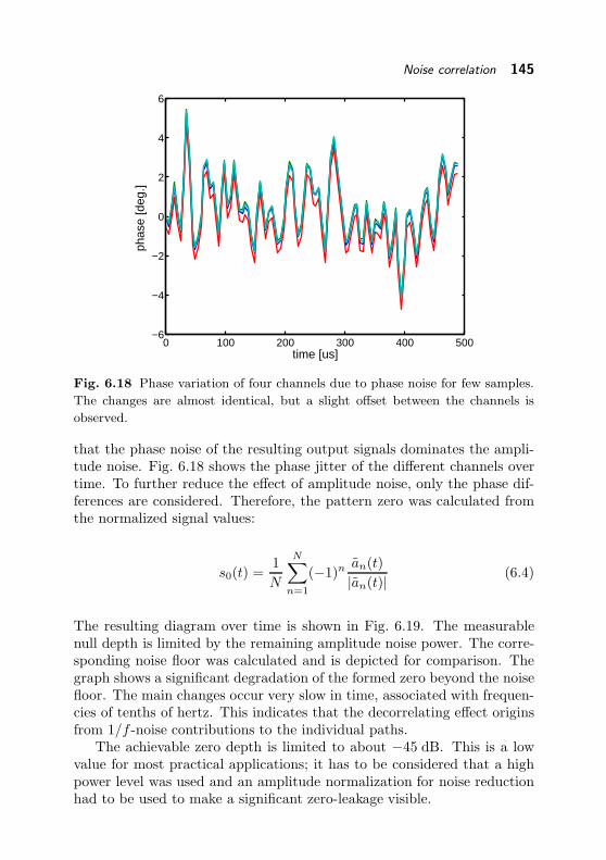
Noise correlation 145
0 100 200 300 400 500−6
−4
−2
0
2
4
6
time [us]
phas
e [d
eg.]
Fig. 6.18 Phase variation of four channels due to phase noise for few samples.
The changes are almost identical, but a slight offset between the channels is
observed.
that the phase noise of the resulting output signals dominates the ampli-tude noise. Fig. 6.18 shows the phase jitter of the different channels overtime. To further reduce the effect of amplitude noise, only the phase dif-ferences are considered. Therefore, the pattern zero was calculated fromthe normalized signal values:
s0(t) =1
N
N∑
n=1
(−1)n an(t)
|an(t)|(6.4)
The resulting diagram over time is shown in Fig. 6.19. The measurablenull depth is limited by the remaining amplitude noise power. The corre-sponding noise floor was calculated and is depicted for comparison. Thegraph shows a significant degradation of the formed zero beyond the noisefloor. The main changes occur very slow in time, associated with frequen-cies of tenths of hertz. This indicates that the decorrelating effect originsfrom 1/f -noise contributions to the individual paths.
The achievable zero depth is limited to about −45 dB. This is a lowvalue for most practical applications; it has to be considered that a highpower level was used and an amplitude normalization for noise reductionhad to be used to make a significant zero-leakage visible.
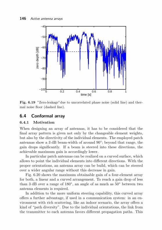
146 Active antenna arrays
0 0.2 0.4 0.6 0.8 1−100
−90
−80
−70
−60
−50
−40
time [s]
zero
dep
th [d
B]
Fig. 6.19 ”Zero-leakage”due to uncorrelated phase noise (solid line) and ther-
mal noise floor (dashed line).
6.4 Conformal array
6.4.1 Motivation
When designing an array of antennas, it has to be considered that thefinal array pattern is given not only by the changeable element weights,but also by the directivity of the individual elements. The employed patchantennas show a 3 dB beam-width of around 90; beyond that range, thegain drops significantly. If a beam is steered into these directions, theachievable maximum gain is accordingly lower.
In particular patch antennas can be realized on a curved surface, whichallows to point the individual elements into different directions. With theproper orientations, an antenna array can be build, which can be steeredover a wider angular range without this decrease in gain.
Fig. 6.20 shows the maximum obtainable gain of a four-element arrayfor both, a linear and a curved arrangement. To reach a gain drop of lessthan 3 dB over a range of 180, an angle of as much as 50 between twoantenna elements is required.
In addition to the more uniform steering capability, this curved arrayoffers a further advantage, if used in a communication system: in an en-vironment with rich scattering, like an indoor scenario, the array offers akind of “path diversity”. Due to the individual orientations, the link fromthe transmitter to each antenna favors different propagation paths. This
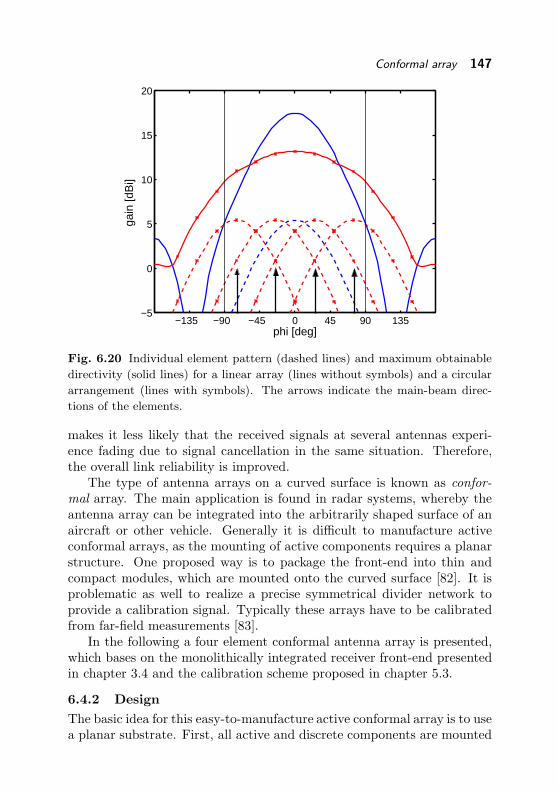
Conformal array 147
−135 −90 −45 0 45 90 135−5
0
5
10
15
20
phi [deg]
gain
[dB
i]
Fig. 6.20 Individual element pattern (dashed lines) and maximum obtainable
directivity (solid lines) for a linear array (lines without symbols) and a circular
arrangement (lines with symbols). The arrows indicate the main-beam direc-
tions of the elements.
makes it less likely that the received signals at several antennas experi-ence fading due to signal cancellation in the same situation. Therefore,the overall link reliability is improved.
The type of antenna arrays on a curved surface is known as confor-mal array. The main application is found in radar systems, whereby theantenna array can be integrated into the arbitrarily shaped surface of anaircraft or other vehicle. Generally it is difficult to manufacture activeconformal arrays, as the mounting of active components requires a planarstructure. One proposed way is to package the front-end into thin andcompact modules, which are mounted onto the curved surface [82]. It isproblematic as well to realize a precise symmetrical divider network toprovide a calibration signal. Typically these arrays have to be calibratedfrom far-field measurements [83].
In the following a four element conformal antenna array is presented,which bases on the monolithically integrated receiver front-end presentedin chapter 3.4 and the calibration scheme proposed in chapter 5.3.
6.4.2 Design
The basic idea for this easy-to-manufacture active conformal array is to usea planar substrate. First, all active and discrete components are mounted

148 Active antenna arrays
rece
iver
rece
iver
rece
iver
rece
iver
LO
IF1 IF2 IF3 IF4
attenuator
CAL2CAL1 linecalibration
Fig. 6.21 System block diagram of the conformal active array. Completely
integrated active front-ends are used to minimize the area consumption. The
transmission-line calibration method is used to calibrate the array. A microstrip
crossing provides the needed signal coupling.
using standard methods, before the array is bent into the wanted shape.Those areas, that remain planar in the final array, can be used for circuitrylike standard microstrip substrates. Inside the regions that are bent nocomponents can be mounted, as these would not remain attached; trans-mission lines have to be placed carefully. This significantly reduces thesubstrate area which is available for circuit placement.
To overcome the problem of the limited space, the monolithically inte-grated receivers described in chapter 3.4 are employed for each of the fourreceiver branches. As it can be seen in the block diagram in Fig. 6.21, theantennas are directly connected to the monolithic receivers.
To avoid a symmetric divider network, the calibration inputs of thereceivers are not used here. Although the changes are found to be small,the unused inputs are terminated with 50 Ω loads. Instead of this classicalcalibration signal distribution, the transmission line calibration methodproposed in chapter 5.3 is used. The coupling between the calibrationline and the receiver branches is achieved by a simple crossing of thetransmission lines, where the interrupted calibration line is bridged by abond wire. Varying the distance between the line ends and the continuoustransmission line, the capacitive coupling between both can be adjusted.Here, gaps of 100 µm length are chosen, resulting in a coupling loss ofaround 25 dB at 5.5 GHz. The two end capacitances together with thebond-wire inductance act as a discrete transmission line equivalent and,therefore, do not introduce any electrical discontinuity into the calibrationline structure.

Conformal array 149
subtrate
patchsubstrate
screws
r=29 mm
r=5 mm
d=27
.3m
mcircuitside
mechanicalsupport
Fig. 6.22 Sketch of the mechanical support for the bent substrate. The antenna
elements are arranged on a circle. The substrate is fixed at both sides of the
bend by screws and the solid antenna substrate. This prevents a bending of the
planar parts, where the components are mounted.
As already mentioned in chapter 5.3, the precision of the proposed cali-bration line method is degraded by reflections, which cause back-travellingwaves on the transmission line. To mitigate possible reflections at the endof the line, two 15 dB attenuators are added.
To demonstrate the feasibility, a large angle of 50 between two el-ements is chosen. As demonstrated in Fig. 6.20, this allows a coverageof 180 degree with a gain decrease of less than 3 dB. Experimentally itwas found, that a bending radius of 5 mm is possible without mechan-ically damaging the Duroid 6010 substrate (εr = 10.2, h = 635 µm) orthe 17 µm thin copper film. This leads to the arrangement depicted inFig. 6.22: the four patches are arranged as tangents on a circle at thecorresponding angles. A mechanical support defines the final shape ofthe array and the 5 mm bending radius. At both sides of the bend, thesubstrate is attached to this support to avoid a bending of these planarparts. This is important, as a bending of these parts could cause the activecircuitry to fail. In the remaining areas, the material of the supportingstructure is removed to allow the placement of undisturbed high frequencytransmission lines on the substrate. The distance from center to center oftwo adjacent patches is set to 27.3 mm, which is approximately half of thefree space wavelength λ0 at 5.5 GHz.
Fig. 6.23 shows the planar circuit layout before the substrate is bent.The four identical receiver branches can easily be identified. Also the
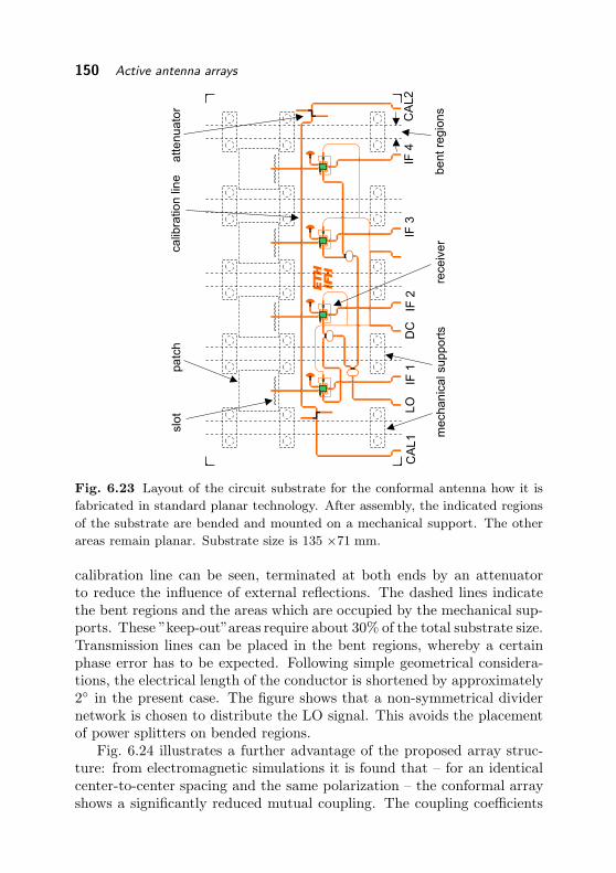
150 Active antenna arrays
pa
tch
slo
ta
tte
nu
ato
rca
libra
tio
n lin
e
CA
L1
CA
L2
LO
IF 1
IF 2
IF 3
IF 4
me
ch
an
ica
l su
pp
ort
sb
en
t re
gio
ns
rece
ive
r
DC
Fig. 6.23 Layout of the circuit substrate for the conformal antenna how it is
fabricated in standard planar technology. After assembly, the indicated regions
of the substrate are bended and mounted on a mechanical support. The other
areas remain planar. Substrate size is 135 ×71 mm.
calibration line can be seen, terminated at both ends by an attenuatorto reduce the influence of external reflections. The dashed lines indicatethe bent regions and the areas which are occupied by the mechanical sup-ports. These ”keep-out”areas require about 30% of the total substrate size.Transmission lines can be placed in the bent regions, whereby a certainphase error has to be expected. Following simple geometrical considera-tions, the electrical length of the conductor is shortened by approximately2 in the present case. The figure shows that a non-symmetrical dividernetwork is chosen to distribute the LO signal. This avoids the placementof power splitters on bended regions.
Fig. 6.24 illustrates a further advantage of the proposed array struc-ture: from electromagnetic simulations it is found that – for an identicalcenter-to-center spacing and the same polarization – the conformal arrayshows a significantly reduced mutual coupling. The coupling coefficients
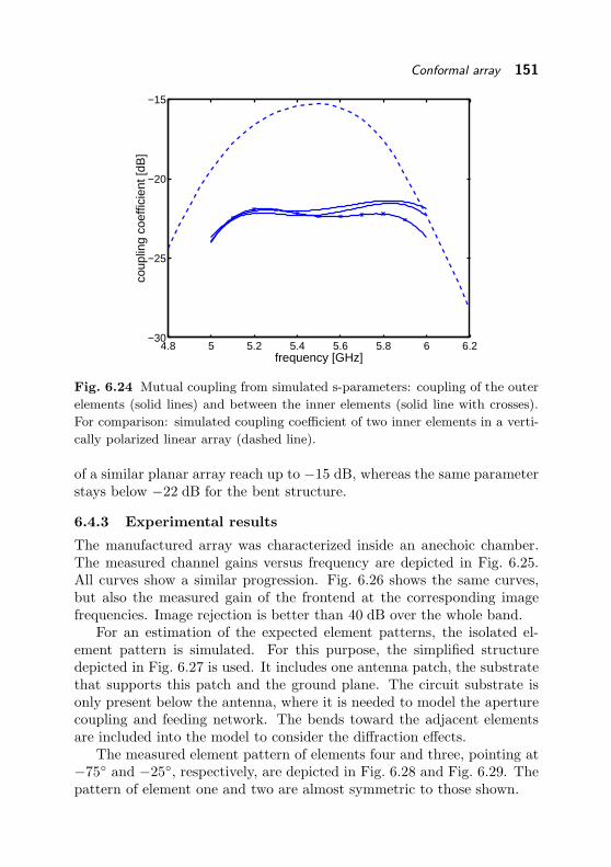
Conformal array 151
4.8 5 5.2 5.4 5.6 5.8 6 6.2−30
−25
−20
−15
frequency [GHz]
coup
ling
coef
ficie
nt [d
B]
Fig. 6.24 Mutual coupling from simulated s-parameters: coupling of the outer
elements (solid lines) and between the inner elements (solid line with crosses).
For comparison: simulated coupling coefficient of two inner elements in a verti-
cally polarized linear array (dashed line).
of a similar planar array reach up to −15 dB, whereas the same parameterstays below −22 dB for the bent structure.
6.4.3 Experimental results
The manufactured array was characterized inside an anechoic chamber.The measured channel gains versus frequency are depicted in Fig. 6.25.All curves show a similar progression. Fig. 6.26 shows the same curves,but also the measured gain of the frontend at the corresponding imagefrequencies. Image rejection is better than 40 dB over the whole band.
For an estimation of the expected element patterns, the isolated el-ement pattern is simulated. For this purpose, the simplified structuredepicted in Fig. 6.27 is used. It includes one antenna patch, the substratethat supports this patch and the ground plane. The circuit substrate isonly present below the antenna, where it is needed to model the aperturecoupling and feeding network. The bends toward the adjacent elementsare included into the model to consider the diffraction effects.
The measured element pattern of elements four and three, pointing at−75 and −25, respectively, are depicted in Fig. 6.28 and Fig. 6.29. Thepattern of element one and two are almost symmetric to those shown.

152 Active antenna arrays
5 5.2 5.4 5.6 5.8 610
15
20
25
30
35
freq [GHz]
gain
[dB
i]
Fig. 6.25 Total frontend gain compared to isotropic radiator. Channel 1 (solid
line with crosses), channel 2 (with diamonds), channel 3 (with circles) and chan-
nel 4 (with squares).
5 5.2 5.4 5.6 5.8 6−60
−50
−40
−30
−20
−10
0
10
20
30
40
freq [GHz]
gain
[dB
i]
Fig. 6.26 Frontend gain at signal band (solid lines) and image band (dashed
lines). Channel 1 (with crosses), channel 2 (with diamonds), channel 3 (with
circles) and channel 4 (with squares).
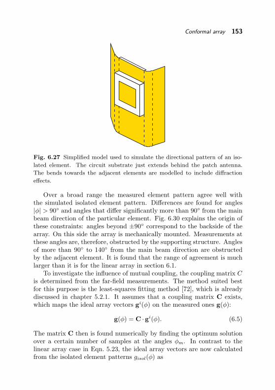
Conformal array 153
Fig. 6.27 Simplified model used to simulate the directional pattern of an iso-
lated element. The circuit substrate just extends behind the patch antenna.
The bends towards the adjacent elements are modelled to include diffraction
effects.
Over a broad range the measured element pattern agree well withthe simulated isolated element pattern. Differences are found for angles|φ| > 90 and angles that differ significantly more than 90 from the mainbeam direction of the particular element. Fig. 6.30 explains the origin ofthese constraints: angles beyond ±90 correspond to the backside of thearray. On this side the array is mechanically mounted. Measurements atthese angles are, therefore, obstructed by the supporting structure. Anglesof more than 90 to 140 from the main beam direction are obstructedby the adjacent element. It is found that the range of agreement is muchlarger than it is for the linear array in section 6.1.
To investigate the influence of mutual coupling, the coupling matrix Cis determined from the far-field measurements. The method suited bestfor this purpose is the least-squares fitting method [72], which is alreadydiscussed in chapter 5.2.1. It assumes that a coupling matrix C exists,which maps the ideal array vectors gi(φ) on the measured ones g(φ):
g(φ) = C ·gi(φ). (6.5)
The matrix C then is found numerically by finding the optimum solutionover a certain number of samples at the angles φm. In contrast to thelinear array case in Eqn. 5.23, the ideal array vectors are now calculatedfrom the isolated element patterns gisol(φ) as
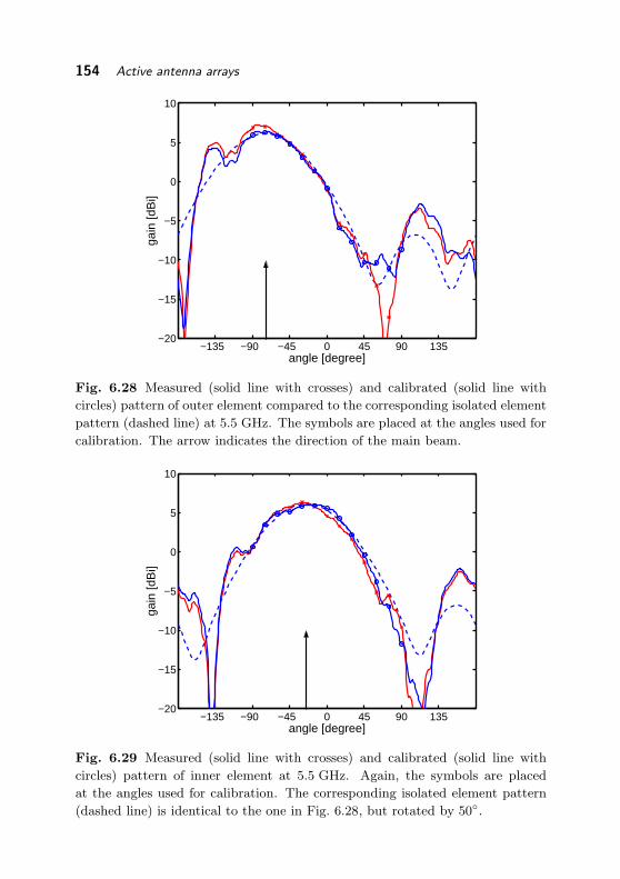
154 Active antenna arrays
−135 −90 −45 0 45 90 135−20
−15
−10
−5
0
5
10
angle [degree]
gain
[dB
i]
Fig. 6.28 Measured (solid line with crosses) and calibrated (solid line with
circles) pattern of outer element compared to the corresponding isolated element
pattern (dashed line) at 5.5 GHz. The symbols are placed at the angles used for
calibration. The arrow indicates the direction of the main beam.
−135 −90 −45 0 45 90 135−20
−15
−10
−5
0
5
10
angle [degree]
gain
[dB
i]
Fig. 6.29 Measured (solid line with crosses) and calibrated (solid line with
circles) pattern of inner element at 5.5 GHz. Again, the symbols are placed
at the angles used for calibration. The corresponding isolated element pattern
(dashed line) is identical to the one in Fig. 6.28, but rotated by 50.
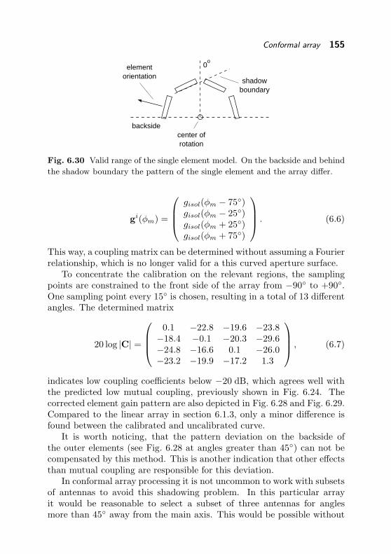
Conformal array 155
backsidecenter ofrotation
orientationelement
boundaryshadow
0o
Fig. 6.30 Valid range of the single element model. On the backside and behind
the shadow boundary the pattern of the single element and the array differ.
gi(φm) =
gisol(φm − 75)gisol(φm − 25)gisol(φm + 25)gisol(φm + 75)
. (6.6)
This way, a coupling matrix can be determined without assuming a Fourierrelationship, which is no longer valid for a this curved aperture surface.
To concentrate the calibration on the relevant regions, the samplingpoints are constrained to the front side of the array from −90 to +90.One sampling point every 15 is chosen, resulting in a total of 13 differentangles. The determined matrix
20 log |C| =
0.1 −22.8 −19.6 −23.8−18.4 −0.1 −20.3 −29.6−24.8 −16.6 0.1 −26.0−23.2 −19.9 −17.2 1.3
, (6.7)
indicates low coupling coefficients below −20 dB, which agrees well withthe predicted low mutual coupling, previously shown in Fig. 6.24. Thecorrected element gain pattern are also depicted in Fig. 6.28 and Fig. 6.29.Compared to the linear array in section 6.1.3, only a minor difference isfound between the calibrated and uncalibrated curve.
It is worth noticing, that the pattern deviation on the backside ofthe outer elements (see Fig. 6.28 at angles greater than 45) can not becompensated by this method. This is another indication that other effectsthan mutual coupling are responsible for this deviation.
In conformal array processing it is not uncommon to work with subsetsof antennas to avoid this shadowing problem. In this particular arrayit would be reasonable to select a subset of three antennas for anglesmore than 45 away from the main axis. This would be possible without
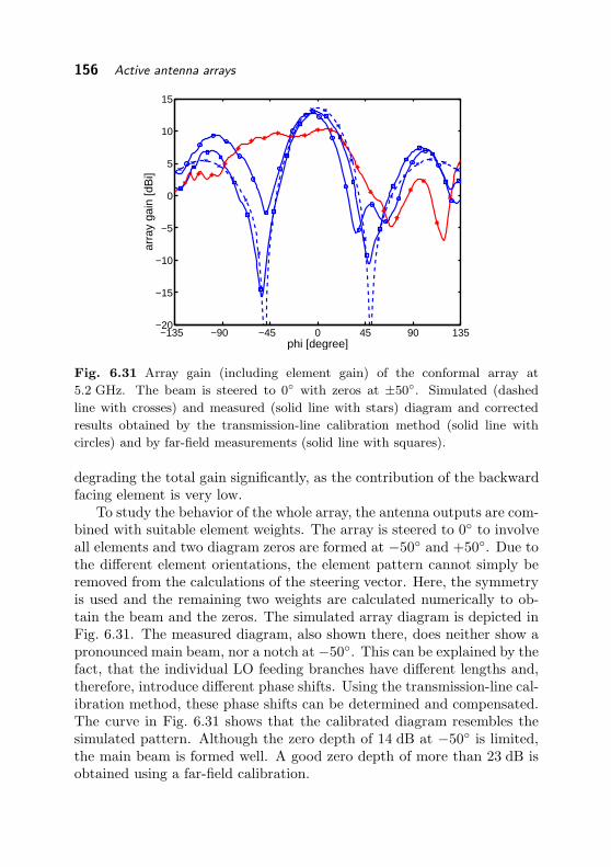
156 Active antenna arrays
−135 −90 −45 0 45 90 135−20
−15
−10
−5
0
5
10
15
phi [degree]
arra
y ga
in [d
Bi]
Fig. 6.31 Array gain (including element gain) of the conformal array at
5.2 GHz. The beam is steered to 0 with zeros at ±50. Simulated (dashed
line with crosses) and measured (solid line with stars) diagram and corrected
results obtained by the transmission-line calibration method (solid line with
circles) and by far-field measurements (solid line with squares).
degrading the total gain significantly, as the contribution of the backwardfacing element is very low.
To study the behavior of the whole array, the antenna outputs are com-bined with suitable element weights. The array is steered to 0 to involveall elements and two diagram zeros are formed at −50 and +50. Due tothe different element orientations, the element pattern cannot simply beremoved from the calculations of the steering vector. Here, the symmetryis used and the remaining two weights are calculated numerically to ob-tain the beam and the zeros. The simulated array diagram is depicted inFig. 6.31. The measured diagram, also shown there, does neither show apronounced main beam, nor a notch at −50. This can be explained by thefact, that the individual LO feeding branches have different lengths and,therefore, introduce different phase shifts. Using the transmission-line cal-ibration method, these phase shifts can be determined and compensated.The curve in Fig. 6.31 shows that the calibrated diagram resembles thesimulated pattern. Although the zero depth of 14 dB at −50 is limited,the main beam is formed well. A good zero depth of more than 23 dB isobtained using a far-field calibration.

Conclusions 157
Fig. 6.32 Photography of the manufactured active conformal antenna array.
Fig. 6.32 shows a photograph of the fabricated active conformal an-tenna array. One can clearly see the patch antennas pointing at individualangles. The metal strips in the lower part are used to reinforce the sub-strate and give a good hold to the connectors. The circles in the centerbelong to the ground vias connected to the receiver chips, which reside onthe opposite, non-visible side.
6.5 Conclusions
In this chapter, active antenna arrays are presented, which employ themonolithically integrated front-ends that were presented in chapter 3. Asintended, an excellent long-term stability of gain and phase transfer func-tions is achieved with the integration of the critical high frequency process-ing into the antenna array. The remaining gain and phase variations aremainly due to changes of the ambient temperature and are well correlated.
It is found, that the phase variations caused by phase noise also arewell correlated. The ”zero-leakage”resulting from uncorrelated phase noisestays fairly low and does not affect the practical application. This opens
158 Active antenna arrays
the way for a more aggressive design. If the specifications are relaxed anda certain amount of uncorrelated phase noise is intentionally tolerated, thesystem could benefit in other areas. E.g., it is possible to replace the linearLO amplifiers by highly efficient nonlinear class-C amplifiers to reduce thepower consumption. It could also be attractive to use phase-locked-loopsto generate the LO signals locally for each branch from a common low-frequency reference. This would replace the last remaining high-frequencyinterconnections.
On a four element aperture-coupled patch antenna array with 45-slanted polarization it is demonstrated, that the mutual coupling can bedescribed and compensated by a suitable coupling matrix. The behaviorof this calibrated array can be described by the simple geometrical arraymodel with a reasonable precision. For this particular array, the agreementis limited to an angular range of less than ±60 from the array broadsidedirection. Beyond that range the individual element pattern differ fromthe pattern of an isolated element in a way, which can not be explainedby mutual coupling.
The high integration of the RF hardware allows to construct a newtype of active conformal arrays. The individual orientation of the arrayelements allows to distribute the maximum obtainable beamforming gainmore uniformly over a larger angular range. A conformal array is demon-strated, which covers a range of 180 degree with less than 3 dB decrease ofgain. This array inherently exhibits a significantly lower mutual coupling.Furthermore, the geometrical array model is valid for a larger range. Ifsubsets of three antennas are chosen and the element facing to the oppo-site side is not considered, the geometrical model can be used over thecomplete 180 range.

7
Summary, conclusions andoutlook
The following sections list the main results achieved in this dissertationand indicate some directions for future work on this subject.
7.1 System design
Chapter 2 presents the system-level design of a multiple-channel receiverfor 5.15 –5.875 GHz. To obtain a modular and flexible system, a super-heterodyne architecture is chosen. To solve the problem of image filteringwithout the need for external components, a high intermediate frequencyis selected and the mirror band is placed to a quiet region. The imple-mentation aspects of a multi-channel system are discussed with a focuson the noise correlation in such a system. For the application in a multi-dimensional channel-sounder, minimum noise contribution of the frontendis required. It is found that the required mixer is the key component toreach a good linearity and a low noise-figure simultaneously. The use ofa passive resistive mixer is proposed to reach a high dynamic range. Allthese considerations lead to the specifications of the single circuit blocks.
7.2 Integrated circuit design
Chapter 3 describes the implementation of the active downconverter. Thedifferent building blocks are integrated on a commercially available 0.6 µmGaAs MESFET process. The key components are a three-stage low-noiseamplifier with 22 dB gain and 2.4 dB noise figure and in input compressionpoint of −16.5 dBm, a resistive mixer with 6.8 dB conversion loss and aninput compression point of 4 dBm at a required LO power of 10 dBm anda downconverter with 7 dB conversion gain at a required LO power level of5 dBm and an input compression point of 1 dBm. The complete frontendis integrated, including a lumped element image filter. For this completereceiver, the following key parameters are measured: at 5.5 GHz the con-version gain is 26 dB for an LO power higher than 0 dBm. The input

160 Summary, conclusions and outlook
1 dB-compression point is higher than −18 dB. Over the band of interest,the single-sideband noise-figure is below 3.8 dB and the image rejectionis between 35 dB and 50 dB. Both are remarkable results for integratedreceivers. To avoid a passive switch and the associated higher noise figurefor system calibration, an active switching concept is proposed. A channelmismatch of less than 0.7 dB over the whole band can be achieved usinga symmetrical layout. The whole system draws 76 mA from a 3 V supplyand requires 3.2 mm2 of chip area. On the same process, a power amplifierwith an integrated temperature monitoring diode is designed to study thedynamic behavior of the calibration in transmit arrays. To evaluate thecapability of silicon-based technologies, a 10.7 –11.7 GHz downconverteris designed on a low-ft SiGe process. A gain of 15 dB, a noise figure ofless than 4 dB and an input compression point of −12.7 dBm are foundfor the low-noise amplifier alone. Utilizing the MOSFET as a resistivemixer, a complete receiver is integrated and a conversion gain of 10 dB, asingle-sideband noise-figure of 7 dB and an input 1 dB-compression pointof −14 dBm are measured. The power consumption is 27.6 mA from a3.3 V supply and the circuit requires an area of 1.75 mm2. The dynamicrange of this receiver is significantly larger than other published receiveron comparable technologies, which all base on active mixers.
7.3 Passive arrays
Chapter 4 focuses on the passive antenna structure. The choice of aperture-coupled patch antennas is motivated, for which an equivalent circuit modelcan be found that supports the design process. With the help of thismodel, an antenna layout is determined, which achieves the required band-width. For compatibility with differential integrated circuits, which are ad-vantageous for mixed-signal applications and on technologies with strongsubstrate cross-talk, a differential antenna interface is proposed. The mu-tual coupling is discussed and classified. For linear arrays of aperture-coupled patch antennas it is verified by simulations that assumption ofa well-behaved array can be made. This allows to describe the far-fieldpattern of the array by the superposition of identical element patterns,which equal the pattern of a single isolated element. The coupling can bedescribed by a coupling matrix C, which also allows to compensate thiseffect. To simulate the consequence of a mismatch at the antenna feed-ing points, the equivalent circuit model for the antenna is extended bymutual coupling. It is experimentally demonstrated that the interface be-tween antenna and amplifier in an active array can be optimized to lowerthe mutual coupling.

Calibration 161
7.4 Calibration
In chapter 5 various practical aspects of the calibration of antenna arraysare discussed. To assess the required precision, the typical element varia-tions and error effects are reviewed. An overview is given over the availablecalibration schemes, which can be subdivided into methods which use far-field sources and those which use a local reference signal. The far-fieldmethods include the effect of mutual coupling, but an anechoic environ-ment is needed. Considering the fact that the main changes of the transferfunctions are caused by the active hardware, it is attractive to perform atwo-step calibration: the passive array is characterized once from measure-ments or simulations and the local calibration signal is used to track thereceiver changes. To simplify the calibration network for two-dimensionalor arbitrary array arrangements, a new calibration method is proposedthat employs a local coupling between all branches provided by a weaklycoupled transmission line, which links all elements. The determinationof the transmission factors of the line segments is part of the calibrationprocess itself. The dynamic effect of switched power amplifiers on the cali-bration of transmit arrays is studied. For monolithically integrated poweramplifiers two thermal time-constants are experimentally found. A typicalburst up to a duration of milliseconds can be calibrated using a single setof correction values. If the duty cycle stays constant, the obtained valuescan be reused for several pulses. For a changed duty cycle the variationsare less correlated and a slight pattern variation occurs.
7.5 Active antenna arrays
Chapter 6 deals with the final integration of the monolithic receivers pre-sented in chapter 3 and the passive array discussed in chapter 4 andsystem-level measurements are performed on these active frontends. Anexcellent long-term stability of gain and phase transfer functions is found.The gain and phase variations are mainly due to changes of the ambi-ent temperature and are well correlated. The phase variations caused byphase noise also are well correlated. The zero-leakage resulting from un-correlated phase noise stays fairly low and does not affect the practicalapplication. For a four-element array with 45-slanted polarization it isdemonstrated, that a good calibration can be achieved over a range of±60 from the array broadside direction. This coincides approximatelywith the beam-width of the antenna elements. An active conformal arrayis designed, which covers a range of 180 degree with less than 3 dB de-crease of gain. This array inherently exhibits a significantly lower mutualcoupling. Due to the curved surface, the individual element pattern agreewith the isolated element pattern over a larger angular range.

162 Summary, conclusions and outlook
7.6 Conclusions and future work
The developed active antenna arrays benefit from the monolithic inte-gration of the critical RF frontends. A compact and robust solution isobtained, which allows to construct uniform linear arrays as well as morefreely arranged arrays. The novel transmission line calibration methodhelps to simplify the design of these arrays.
The elimination of high-frequency transmission lines and connectorsleads to a very good long-term stability of the individual transfer functions.Thanks to the good reproducibility of monolithically integrated circuitsnot only similar path responses are achieved, but also all changes are wellcorrelated. This ensures that the negative effect on beamforming is verylow and the interferer rejection capability is not significantly degraded.Long time intervals between the calibrations can be tolerated. This is ofspecial interest in transmit arrays: rapid temperature changes in switchedpower amplifiers could cause a pattern degradation, which can be avoidedusing identical monolithic amplifiers.
The presented system is consequently designed for a low noise-figureand well synchronized phases of the transfer functions. The system-levelanalysis of the multi-channel phase noise indicates that a very good corre-lation of the phases is achieved, the phase errors of the individual branchesare not significant for most applications. For a future system it is advis-able to specify a tolerated phase deviation due to individual phase noisecontributions. Adjusting the system architecture, this parameter can betraded off against other advantages: nonlinear LO amplifiers could reducethe power consumption, or an integrated phase-locked loop could be ap-plied to generate the LO signal locally. Both options increase the amountof uncorrelated phase noise. The integration of a phase-locked loop wouldfurther reduce the number of off-chip high-frequency connections. This be-comes increasingly attractive at higher operating frequencies, which willbe required to address the growing bandwidth demands in the future. TheSiGe technology appears suitable to combine the analog frontend and therequired digital phase-detector and frequency divider. A differential cir-cuit design, which minimizes the noise cross-talk, could benefit from theproposed differential antenna interface.
In the presented system the antenna arrangement was selected for therequirements of classical beamforming, being a suboptimal choice for aMIMO system. With the example of a conformal array it has been demon-strated that arrangements different from uniform linear arrays can be re-alized, which are advantageous in certain scenarios.

Bibliography
[1] P.K. Bondyopadhyay, ”The First Application of Array Antenna”,IEEE Int. Conf. on Phased Array Systems and Technology, p. 29,may 2000
[2] D. Parker, D. C. Zimmermann, “Phased-Arrays–Part1: Theory andArchitectures”, IEEE T. on Microwave Theory and Techniques, vol.50, no. 3, p. 678, mar. 2002
[3] D. Parker, D. C. Zimmermann, “Phased-Arrays–Part2: Implemen-tations, Applictions, and Future Trends”, IEEE T. on MicrowaveTheory and Techniques, vol. 50, no. 3, p. 688, mar. 2002
[4] G. Tsoulos, J. McGeehan, M. Beach, “Space division multiple access(SDMA) field trials. I. Tracking and BER performance”, IEE Proc.Radar, Sonar and Navigation, vol. 145, iss. 1, p. 73, feb. 1998
[5] G. Tsoulos, J. McGeehan, M. Beach, “Space division multiple access(SDMA) field trials. II. Calibration and linearity issues”, IEE Proc.Radar, Sonar and Navigation, vol. 145, iss. 1, p. 79, feb. 1998
[6] S. Anderson, U. Forssen, J. Karlsson, T. Witzschel, P. Fischer,A. Krug, “Ericsson/Mannesmann GSM field-trials with adaptiveantennas”, IEEE Vehicular Technology Conference, vol. 3, p. 1587,may 1997
[7] J.J. Monot, J. Thibault, P. Chevalier, F. Pipon, S. Mayrargue,A. Levy, “A fully programmable prototype for the experimentationof the SDMA concept and use of smart antennas for UMTS andGSM/DCS1800 networks”, IEEE Int. Symp. Personal, Indoor andMobile Radio Communications, vol. 2, p. 534, sept. 1997
[8] A. O. Boukalov, S.-G. Haggman, “System Aspects of Smart-AntennaTechnology in Cellular Wireless Communications–An Overview”,IEEE T. on Microwave Theory and Techniques, vol. 48, no. 6, p.919, june. 2000
[9] G. J. Foschini, “Layered space-time architecture for wireless com-munication in a fading envionment when using multi-element an-tennas”, Bell Labs Tech. J., vol. 1, no 2, p. 41, autumn 1996
[10] S. M. Alamouti, “A Simple Transmit Diversity Technique for Wire-

164 BIBLIOGRAPHY
less Communications”, IEEE J. on Selected Areas in Communica-tions, vol. 16, no. 8, oct. 1998
[11] G. J. Foschini, D. Chizhik, M. J. Gans, C. Papadias, R. A. Valen-zuela, “Analysis and Performance of Some Basic Space-Time Archi-tectures”, J. on Selected Areas in Communications, vol. 21, no. 3,april 2003
[12] D. Chizhik, J. Ling, P.W. Wolniansky, R.A. Valenzuela, N. Costa,K. Huber, “Multiple-Input–Multiple-Output Measurements andModeling in Manhattan”, J. on Selected Areas in Communications,vol. 21, no. 3, p. 321, april 2003
[13] A. Stucki et. al., ”Propsound System Specifications Document: Con-cept and Specifications”, 2001, Elektrobit AG, www.propsound.com
[14] J. Lin, T. Itoh, “Active Integrated Antennas”, IEEE T. on Mi-crowave Theory and Techniques, vol. 42, no. 12, p. 2186, dec. 1994
[15] “Broadband Radio Access Networks (BRAN); HIPERLAN Type 2;Physical (PHY) layer”, ETSI TS 101 475, technical specification,april 2000
[16] J. Crols, M.S.J. Steyaert, ”Low-IF Topologies for High-PerformanceAnalog Front Ends of Fully Integrated Receivers”, IEEE Trans. onCircuits and Systems – II: Analog and Digital Signal Processing, vol.45, no. 3, march 1998
[17] F. Ellinger, W. Bachtold, “Adaptive Antenna Receiver Modulefor WLAN at C-Band With Low-Power Consumption”, IEEE Mi-crowave and Wireless Components Letters, vol. 12, no. 9, sept. 2002
[18] S.S. Jeon, Y. Wang, Y. Qian, T. Itoh, “A novel smart antennasystem implementation for broad-band wireless communications”,IEEE Trans. on Antennas and Propagation, vol. 50, iss. 5, p. 600,may 2002
[19] J.D. Fredrick, Y. Wang, T. Itoh, “A smart antenna receiver arrayusing a single RF channel and digital beamforming”, IEEE Trans.on Microwave Theory and Techniques, vol. 50, iss. 12, p. 3052, dec.2002
[20] T. Nishio, Y. Wang, T. Itoh, “Multiple-beam adaptive array archi-tecture using channel-level FDMA concept”, Antennas and Propa-gation Int. Symp., vol. 3, p. 908, june 2003
[21] R. Nabar, ”MIMO wireless communications”, lecture ETH doctoralschool, summer semster 2003
[22] C. Waldschmidt, C. Kuhnert, S. Schulteis, W. Wiesbeck,”CompactMIMO-arrays based on polarisation-diversity”, IEEE Antennas andPropagation Int. Symp., vol. 2, p. 499, june 2003

BIBLIOGRAPHY 165
[23] J. P. Weem, Z. Popovic, ”A method for determining noise couplingin a phased array antenna”, IEEE MTT-S Int. Microwave Symp.2001, vol. 1, p. 271
[24] L. C. Howard, D. J. Rabideau, ”Correlation of Nonlinear Distor-tion in Digital Phased Arrays: Measurement and Mitigation”, IEEEMTT-S Int. Microwave Symp. 2002, vol. 1, p. 49
[25] G. W. Slade, ”Effects of local oscillator phase noise on interferencerejection capability of CDMA receivers using adaptive antenna ar-rays”, IEEE MTT-S Int. Microwave Symp. 2002, vol. 2, p. 1353
[26] D.S. Baum, H. Bolcskei, ”Impact of Phase Noise on MIMO ChannelMeasurement Accuracy”, VTC Fall 2004
[27] J. H. Reed, ”Software Radio”, Prentice Hall, chapter 4, ISBN 0-13-081158-0, 2002
[28] Y. Yamashita, A. Endoh, K. Shinohara, K. Hikosaka,T. Matsui, S. Hiyamizu, T. Mimura, ”PseudomorphicIn0.52Al0.48As/In0.7Ga0.3As HEMTs With an Ultrahigh fT of562 GHz”, IEEE Electron Device Letters, vol. 23, no. 10, oct. 2002
[29] TriQuint Semiconductor, ”TQTRx process information”,http://www.tqs.com
[30] N. Zamdmer, J. Kim, R. Trzcinski, J.-O. Plochart, S. Narasimha,M. Khare, L. Wagner, S. Chaloux, ”A 243-GHz Ft and 208-GHzFmax, 90-nm SOI CMOS SoC technology with low-power millimeter-wave digital and RF circuit capability”, IEEE Symposium on VLSITechnology 2004, accepted for publication
[31] J.-S. Rieh, B. Jagannath, H. Chen, K. Schonenberg, S.-J. Jeng,M. Khater, D. Ahlgren, G. Freeman, S. Subbanna, ”Perfor-mance and Design Considerations for High Speed SiGe HBTs offT /fmax=375GHz/210GHz”, Intern. Conf. on Indium Phosphideand Related Materials, p. 374, 2003
[32] J. j. Kucera, ”Highly Integrated RF transceivers”, Diss. ETHNr. 13361
[33] L.E. Larson, ”Integrated Circuit Technology Options for RFIC’s–Present Status and Future Directions”, IEEE J. of Solid-State Cir-cuits, v. 33, no. 3, p. 387, march 1998
[34] W. Bachtold, ”Mikrowellenelektronik”, Vieweg Verlag, ISBN 3-528-03937-X
[35] H. Jackel, ”Schnelle analoge und digitale Kommunikations-Elektronik I”, lecture script, ETH Zurich
[36] S. A. Maas, ”Microwave Mixers”, Norwood, MA, 1993

166 BIBLIOGRAPHY
[37] S. A. Maas, “A GaAs MESFET Mixer with Very Low Intermodula-tion”, IEEE Trans. on Microwave Theory and Techniques, vol. 35,no. 4, april 1987
[38] F. Ellinger, R. Vogt, W. Bachtold, ”Compact Monolithic IntegratedResistive Mixers With Low Distortion for HIPERLAN, IEEE T. onMicrowave Theory and Techniques, vol. 50, no. 1, p. 187, jan. 2002
[39] R. Hallgren, P. Litzenberg, ”TOM3 Capacitance Model: LinkingLarge- and Small-Signal MESFET Models in SPICE”, IEEE T. onMicrowave Theory and Techniques, vol. 47, no. 5, p. 556, may. 1999
[40] T. Lee, H. Samavati, H. Rategh, ”5-GHz CMOS Wireless LANs”,IEEE T. on Microwave Theory and Techniques, vol. 50, no. 1, p.286, jan. 2002
[41] B. Razavi, ”A 5.2-GHz CMOS Receiver with 62-dB Image Rejec-tion”, IEEE J. of Solid-State Circuits, vol. 36, no. 5, p. 810, may2001
[42] M. Copeland, S. Voinigescu, D. Marchesan, P. Popescu,M. Maliepaard, ”5-GHz SiGe HBT Monolithic Radio Transceiverwith Tunable Filtering”, IEEE T. on Microwave Theory and Tech-niques, vol. 48, no. 2, , p.170, feb. 2000
[43] J.P. Maligeorgos, J.R. Long, ”A low-voltage 5.1-5.8-GHz Image-Reject Receiver with Wide Dynamic Range”, IEEE J. Solid-StateCircuits, vol. 35, no. 12, dec. 2000
[44] J. Alves Torres, J. Costa Freire, ”Monolithic Transitors SPST Switchfor L-Band”, IEEE T. on Microwave Theory and Techniques, vol.50, no. 1, p. 51, jan. 2002
[45] A. Italia, E. Ragonese, G. Girlando, G. Palmisano, ”A 5–GHz Mono-lithic Silicon Bipolar Down-converter with a 3.2-dB Noise Figure”,IEEE Radio Frequency Integrated Circuits Symposium 2003, p. 453,june 2003
[46] T.-P. Liu, E. Westerwick, ”5-GHz CMOS Radio Transceiver Front-End Chipset”, J. of Solid-State Circuits, vol. 35, no. 12, dec. 2000
[47] J.R. Long, ”A low-voltage 5.1-5.8-GHz Image-Reject DownconverterRF IC”, IEEE J. Solid-State Circuits, vol. 35, no. 9, Sept. 2000
[48] S.C. Cripps, “RF Power Amplifiers for Wireless Communications”,Artech House, Norwood, ISBN. 0-89006-989-1, 1999
[49] H. Ku, M.D. McKinley, J.S. Kenney, “Quantifying memory effectsin RF power amplifiers”, IEEE Trans. on Microwave Theory andTechniques, vol. 50, no. 12, dec. 2002
[50] S.Y. Liao, “Microwave Circuit Analysis and Amplifier Design”,Prentice Hall, 1984

BIBLIOGRAPHY 167
[51] D. Zoschg, W. Wilhelm, T.F. Meister, J. Knapp, H.-D. Wohlmuth,K. Aufinger, M. Wurzer, J. Bock, H. Schafer, A. Scholz, ”2dB noisefigure, 10.5GHz LNA using SiGe bipolar technology”, ElectronicsLetters, vol. 35, no. 25, dec. 1999
[52] U. Erben, H. Schumacher, A. Schuppen, H. Dietrich, J. Arndt, ”Ap-plication of a Production Ready SiGe HBT Process to 1.9, 5.7 and10 GHz Low Noise MMIC’s”, Topical Meeting on Silicon MonolithicIntegrated Circuits in RF Systems, p. 100, sept. 1998
[53] W. Durr, U. Erben, A. Schuppen, H. Dietrich, H. Schumacher,”Low-power low-noise active mixers for 5.7 and 11.2 GHz usingcommercially available SiGe HBT MMIX technology”, ElectronicsLetters, vol. 34, no. 21, oct. 1998
[54] M.W. Lynch, C.D. Holdenried, J.W. Haslett, ”A 17-GHz DirectDown-Conversion Mixer in a 47-GHz SiGe Process”, IEEE RadioFrequency Integrated Circuits Symposium, p. 461, june 2003
[55] K.B. Schad, H. Schumacher, A. Schuppen, ”Low-power active mixerfor Ku-Band application using SiGe HBT MMIC technology”, IEEERadio Frequency Integrated Circuits Symposium, p. 263, june 2000
[56] E. Sonmez, A. Trasser, K.B. Schad, P. Abele, H. Schumacher, ”Asingle-chip 24 GHz receiver front-end using a commercially avail-able SiGe HBT foundry process”, IEEE Radio Frequency IntegratedCircuits Symposium, p. 159, june 2002
[57] IBM, ”Blue Logic BiCMOS 6HP Technology”, available online:www.chips.ibm.com
[58] J.-F. Zurcher, ”The SSFIP, a Global Concept for High PerformanceBroadband Planar Antennas”, Electronics Letters, vol. 24, 1988
[59] J.-F. Zurcher, F. Gardiol, ”Broadband patch antennas”, ArctechHouse, 1995
[60] W.J. Getsinger, ”Measurement and Modeling of the Apparent Char-acteristic Impedance of Microstrip”, IEEE Trans. on MicrowaveTheory and Techniques, vol. 83, no. 8, aug. 1983
[61] M. Kossel, R. Kung, J. Hansen, W. Bachtold, ”Circular PolarizedAperture-Coupled Patch Antennas for an RFID-System in the 2.4-GHz ISM Band”, Microwave Journal, vol. 42, no. 11, p. 20, 1999
[62] L. Steinemann, “Aperturgekoppelte Patchantenne”, SemesterarbeitIFH, SoSe 2001
[63] W.R. Deal, V. Radisic, Y. Qian, T. Itoh, ”Integrated-Antenna Push-Pull Power Amplifiers”, IEEE T. on Microwave Theory and Tech-niques, vol. 47, no. 8, Aug. 1999

168 BIBLIOGRAPHY
[64] H. An, B.K.J.C. Nauwelaers, A.R. Van De Capelle, R. G. Bosisio, ”Anovel measurement technique for amplifier-type active antennas”,1994 IEEE MTT-S Int. Microwave Symp. Dig. , vol. 3, p. 1473,May 1994
[65] D.M. Pozar, “The Active Element Pattern”, IEEE Trans. on An-tennas and Propagation, vol. 42, no. 8, aug. 1994
[66] D.F. Kelley, W.L. Stutzman, “Array Antenna Pattern ModelingMethods That Include Mutual Coupling Efffects”, IEEE Trans. onAntennas and Propagation, vol. 41, no. 12, dec. 1993
[67] H. Steyskal, J.S. Herd, “Mutual Coupling Compensation in SmallArray Antennas”, IEEE Trans. on Antennas and Propagation, vol.38, no. 12, dec. 1990
[68] D. Parker, D. C. Zimmermann, “Phased Arrays–Part 1: Theory andArchitectures”, IEEE Trans. on Microwave Theory and Techniques,vol. 50, no. 3, march 2002
[69] H. Aumann, F.G. Willwerth, ”Phased Array Calibration Using Mea-sured Element Patterns”, IEEE Int. Symp. on Antennas and Prop-agation, vol. 2, p. 918, june 1995
[70] W.L. Stutzman, G.A. Thiele, Antenna Theory and Design, JohnWiley & Sons, New York, 1981
[71] R.J. Marks II, ”Advanced Topics in Shannon Sampling and Inter-polation Theory”, Springer-Verlag New York, ISBN 0-387-97906-9
[72] L. Kuehnke, ”Phased Array Calibration Procedures Based on Mea-sured Element Patterns”, IEE Int. Conf. on Antennas and Propa-gation, p. 660, april 2001
[73] A. Kortke, ”A New Calibration Algorithm for Smart Antenna Ar-rays”, IEEE Vehicular Technology Conference, vol. 2, p. 1030, april2003
[74] G.V. Tsoulos, M.A. Beach, ”Calibration and Linearity issues foran Adaptive Antenna System”, IEEE Vehicular Technology Confer-ence, vol. 1, p. 45, 1995
[75] C.M. Simmonds, M.A. Beach, ”Downlink Calibration Requirementsfor the TSUNAMI (II) Adaptive Antenna Testbed”, IEEE Int. Conf.on Personal, Indoor and Mobile Radio Communications, vol. 3, p.1260, 1998
[76] K. Nishimori, K. Cho, Y. Takatori, T. Hori, ”Automatic CalibrationMethod Using Transmitting Signals of an Adaptive Array for TDDSystems”, IEEE Trans. on Vehicular Technology, vol. 50, no. 6, nov.2001

BIBLIOGRAPHY 169
[77] Y. Takeushi, H. Hirayama, K. Fukino, T. Murayama, Y. Notsu,A. Hayashi, ”Auto Calibrated and Distributed Local Loop Config-uration of Array Antenna for CDMA Cellular Base Station”, IEEInt. Symp. on Spread-Spectrum Tech. & Appl., p. 666, sept. 2000
[78] K. Nishimori, K. Cho, Y. Takatori, T. Hori, ”Automatic CalibrationMethod of Adaptive Array Utilizing signal Circulation for LinearArray”, IEEE Vehicular Technology Conference 2001, vol. 3, 2001
[79] H.M. Aumann, A.J. Fenn, F.G. Willwerth, “Phased Array AntennaCalibration and Pattern Prediction Using Mutual Coupling Mea-surements”, IEEE Trans. on Antennas and Propagation, vol. 37,no. 7, july 1989
[80] C. Passmann, F. Hickel, T. Wixforth, ”Investigation of a calibrationconcept for optimum performance of adaptive antenna systems”,IEEE Vehicular Technology Conference, vol. 1, p. 577, may 1998
[81] K.R. Dandekar, H. Ling, G. Xu, ”Smart antenna array calibrationprocedure including amplitude and phase mismatch and mutual cou-pling effects”, IEEE Int. Conf. on Personal, Indoor and WirelessCommunications, p. 293, dec. 2000
[82] M. Schreiner, H. Leier, W. Menzel, H.-P. Feldle, ”Architecture andinterconnect technologies for a novel conformal active phased arrayradar module”, IEEE Int. Microwave Symposium, vol. 1, p. 567,june 2003
[83] J.D. Hanfling, O.J. Bedigian, ”Calibration and test of an active con-formal phased array”, Antennas and Propagation Society Int. Symp.,vol. 3, p. 1142, may 1990


Curriculum vitae
Thomas M. Brauner
born February 8th, 1973in Koln, Germany
School education:
1983-1992 Gymnasium Herkenrath,Bergisch-Gladbach, Germany
Diploma in electrical engineering:
1993-1999 Student of electrical engineering at Aachenuniversity of technology (RWTH Aachen), Germany
1996-1997 Student assistant at the Laboratory forHigh Frequency Technology, RWTH Aachen
1996 Internship at Deutsche Telekom AG, Germany1997 Internship at ASCOM Systec AG, Switzerland1999 Diploma thesis on the verification of a deterministic
propagation model using channel sounding
Doctor of technical sciences:
1999-2004 Research assistant at the Microwave ElectronicsLaboratory (IFH) of the Swiss Federal Institute ofTechnology (ETH), Zurich, Switzerland
1999-2002 Teaching assistant at ETH2004 Dissertation on the implementation of active
antenna frontends for multiple antenna systems


List of publications
T.Brauner, R.Vogt, W.Bachtold, ”A Differential Active Patch AntennaElement for Array Applications”, IEEE Microwave and Wireless Compo-nent Letters, vol. 13, no. 4, p. 161, April 2003
T.Brauner, R.Vogt, W.Bachtold, ”5-6 GHz Monolithically Integrated Cal-ibratable Low-Noise Downconverter for Smart Antenna Arrays”, 2003IEEE Radio Frequency Integrated Circuits Symposium (RFIC), p. 435,June 8-10, 2003, Philadelphia, PA, USA
T.Brauner, R.Kung, R.Vogt, W.Bachtold, ”Noise in Smart Antennas forMobile Communications”, 2003 IEEE Antennas and Propagation Sympo-sium (APS/URSI), vol. 4, p. 184, June 22-27, 2003, Columbus, OH, USA
T.Brauner, R.Kung, R.Vogt, W.Bachtold, ”5-6 GHz Low-Noise ActiveAntenna Array for Multi-Dimensional Channel-Sounding”, 2003 Interna-tional Microwave and Optoelectronics Conference (IMOC 2003), vol. 1,p. 297, September 2003, Foz do Iguazu, Brazil
T.Brauner, R.Vogt, W.Bachtold, ”A Versatile Calibration Method forSmall Active Antenna Arrays”, European Microwave Conference 2003(EuMC 2003), p. 797, October 2003, Munich, Germany
T.Brauner, R.Negra, R.Vogt, W.Bachtold, ”PA Calibration in TDMA An-tenna Arrays”, IEEE Microwave and Wireless Component Letters, ac-cepted for publication


Acknowledgments
I would like to acknowledge the people who supported me during this work.First, I would like to thank my ”Doktorvater” Prof. Werner Bachtold forgiving me the opportunity to work in his research group and profit froma wealth of knowledge and experience. I am also grateful for the valuableinputs from the co-examiners Prof. Helmut Bolcskei and Prof. RolandKung.
A special thank goes to all those people from the IFH, whose technicaland organizational support was indispensable for the successful outcomeof this work; Martin Lanz and Hansruedi Benedickter for bonding andmeasurements, Claudio Maccio and Stephen Wheeler for the mechanicalconstructions and Ray Ballisti, Federico Bonzanigo and Aldo Rossi for thecomputer support. I would like to thank Urs Lott for sharing his know-how and teaching me the first steps in integrated circuit design and RolfVogt, who saved me from an unlucky project.
Furthermore, I am grateful to all people involved into the ”SANTRES”project for the successful cooperation, especially Marcel Wattinger fromElektrobit, Peter Nuchter from Huber & Suhner and Luca Pergola fromthe field theory group.
I especially appreciate all my actual and former colleagues who madethis institute an unforgettable place to stay. Especially I want to mentionthose, who became close friends during this period: Franck, who made atleast my rope reach the summit of Dom, Andrea who revealed for me theuncompromising philosophy of italian cooking and the secret ingredientsand Esteban for his unconventional views on ordinary things and maybethe best climbing days. But also all the others, which are not listed here,should know that I truly enjoyed the open and inspirative atmospherethey all contributed to.
A big thank goes to my parents and my family for their unconditionalsupport. And last I want to thank Laura for always being close, evenwhen there was some euclidian distance between us.


![Printed Multi-Band MIMO Antenna Systems and Their ... · the diversity performance of the MIMO antenna system [3]. A ... Multiple-input-multiple-output (MIMO) antenna systems are](https://static.fdocuments.in/doc/165x107/601832972ff2e95336029d17/printed-multi-band-mimo-antenna-systems-and-their-the-diversity-performance.jpg)