
RFID - Columbia Universitysites.apam.columbia.edu/courses/apph4903x/RFID-Intro.pdf · RFID ......
23
iCLASS ® Optimized to make physical access control more powerful, iCLASS ® 13.56 MHz read/write contactless smart card technology provides versatile interoperability and supports multiple applications such as biometric authentication, cashless payment and PC log-on security. RFID http://www.hidglobal.com 1
-
Upload
phunghuong -
Category
Documents
-
view
217 -
download
2
Transcript of RFID - Columbia Universitysites.apam.columbia.edu/courses/apph4903x/RFID-Intro.pdf · RFID ......

iCLASS®
iCLASS smart cards and readers make access control more powerful and more versatile, o!ering enhanced security through encryption and mutual authentication. At the same time, iCLASS is user-friendly, delivering the convenience, a!ordability and reliability of contactless technology for which HID is known worldwide.
Encrypted CommunicationThe communication between an iCLASS reader and card is encrypted using a secure algorithm so the transaction between the card and reader cannot be “sniffed” and replayed to a reader. The encryption protocol uses a combination of diversified keys, unique 64-bit card serial numbers and mutual card and reader authentication.
Capability to Add Other ApplicationsThe iCLASS chip not only stores HID access control information, it also has memory space available for other applications. iCLASS cards are currently available with 2k bit, 16k, and 32k bit memory capacities, and depending on the amount of memory available and the number of memory areas, iCLASS cards can serve as multi-application credentials that can be used for many purposes. Since the memory can securely store any kind of information, applications for iCLASS include biometrics, secure computer/network authentication, health record management, time and attendance, digital cash (cafeteria & vending) and many, many more.
Imagine an affordable, single-card, contactless solution that allows you to not only read data securely and quickly, but also to securely write data to the card for many applications.
Optimized to make physical access control more powerful, iCLASS® 13.56 MHz read/write contactless smart card technology provides versatile interoperability and supports multiple applications such as biometric authentication, cashless payment and PC log-on security.
RFID
http://www.hidglobal.com1

2

Patch Antenna
US Industrial, Scientific, and Medical (ISM) band from 902-928 MHz
3

4

5

iCLASS®
iCLASS smart cards and readers make access control more powerful and more versatile, o!ering enhanced security through encryption and mutual authentication. At the same time, iCLASS is user-friendly, delivering the convenience, a!ordability and reliability of contactless technology for which HID is known worldwide.
Encrypted CommunicationThe communication between an iCLASS reader and card is encrypted using a secure algorithm so the transaction between the card and reader cannot be “sniffed” and replayed to a reader. The encryption protocol uses a combination of diversified keys, unique 64-bit card serial numbers and mutual card and reader authentication.
Capability to Add Other ApplicationsThe iCLASS chip not only stores HID access control information, it also has memory space available for other applications. iCLASS cards are currently available with 2k bit, 16k, and 32k bit memory capacities, and depending on the amount of memory available and the number of memory areas, iCLASS cards can serve as multi-application credentials that can be used for many purposes. Since the memory can securely store any kind of information, applications for iCLASS include biometrics, secure computer/network authentication, health record management, time and attendance, digital cash (cafeteria & vending) and many, many more.
Imagine an affordable, single-card, contactless solution that allows you to not only read data securely and quickly, but also to securely write data to the card for many applications.
Optimized to make physical access control more powerful, iCLASS® 13.56 MHz read/write contactless smart card technology provides versatile interoperability and supports multiple applications such as biometric authentication, cashless payment and PC log-on security.
Contactless ID
http://www.hidglobal.com6

HID iCLASS Contactless Smart Card presentation - YouTube
Features Specifications
© 2008 HID Global. All rights reserved. HID, the HID logo, and iCLASS are trademarks or registered trademarks of HID Global in the U.S. and/or other countries. All other trademarks, service marks, and product or service names are trademarks or registered trademarks of their respective owners. Rev. 10/2008
ACCESS experience.
HID Global O!ces:
CorporateNorth America 15370 Barranca PkwyIrvine, CA 92618 U.S.A.Phone: (800) 237-7769 Phone: +1 (949) 732-2000Fax: +1 (949) 732-2360
Europe, Middle East & AfricaPhoenix Road Haverhill, Su!olk CB9 7AEEngland Phone: +44 (0) 1440 714 850Fax: +44 (0) 1440 714 840
Asia Pacific19/F 625 King’s RoadNorth PointIsland EastHong KongPhone: +852 3160-9800Fax: +852 3160-4809
Latin AmericaCircunvalacion Ote. #201 B Despacho 2Col. Jardines del MoralLeon 37160, Gto. MexicoPhone: +52 477 779 1492Fax: +52 477 779 1493
hidglobal.com
iCLASS® was specifically designed to make access control more powerful, more versatile, and more secure. All radio frequency data transmission between the card and reader is encrypted using a secure algorithm. By using industry standard encryption techniques, iCLASS reduces the risk of compromised data or duplicated cards. For even higher security, the card data may also be protected with DES or triple DES encryption. Multiple securely separated application areas are each protected by 64-bit diversified read/write keys which allow complex applications and provide for future expansion.
Security mechanisms such as mutual authentication and encryption are e"ciently combined with fast processing and data communica-tion, resulting in transaction times of less than 100 milliseconds for a typical secure e-purse transaction.
O!ers extremely consistent read range. Una!ected by body shielding or variable environmental conditions.
Can be carried with credit cards in a wallet or purse. Use with a strap and clip as a photo ID badge.
Print directly to the card with a direct image or thermal transfer printer. Slot punch vertically for easy use.
Passive, no-battery design allows for an estimated minimum 100,000 reads.
Strong, flexible, and resistant to cracking and breaking.
(Please see “How To Order Guide” for a description of the options and associated part numbers.)
Lifetime warranty. See complete warranty policy for details.
13.56 MHz contactless smart card.
Typical Maximum Read Range*R10 2.0-3.0" (5.0-7.6cm)R30/RW300 2.0-3.5" (5.0-8.9cm)R40/RW400 2.5-4.5" (6.3-11.4cm)RK40/RWK400 3.0-4.0” (7.6-10.1 cm)*Dependent upon installation conditions. Dimensions2.127" x 3.375" x 0.033" max. (5.40 x 8.57 x 0.084 cm)
Weight0.20oz (5.7 g)
Card ConstructionThin, flexible polyvinyl chloride (PVC) laminate.
Operating Temperature-40° to 158° F (-40° to 70° C)
Operating Humidity5-95% non-condensing
Operating Frequency13.56 MHz
RF Interface As suggested by ISO/IEC:15693 read/write 14443B mode - 106 kbps
Transaction Time<100 ms typical
Baud Rate14443 B2 mode - 212 kbps 15693 mode - 26 kbps
Memory TypeEEPROM, read/write
Multi-application Memory2k bit (256 Byte) card – 2 application areas16k bit (2k Byte) card – 2 or 16 application areas32k bit (4k Byte) card – 16k bits in 2 or 16 application areas plus 16k bits user configurable.
Write EnduranceMin. 100,000 cycles
Data Retention10 years
Read/write Functionality for Multi-functional
Memory Applications
Proven, Reliable Technology
Thin
Options:
* Photo ID Compatible
Warranty
Base Part Numbers
Description
Long Life
Durability
MKT-iCLASSCARDS_DS_ENFor best results, pleaseprint on recycled paper.
* When customizing cards using Re-Transfer Printers that fuse images to the surface of the card by applying heat and pressure (such as the Fargo HDP5000) we recommend the use of composite cards, which are better able to withstand the higher application temperatures.
7

About 70¢/Card
8

9

10

ISO/IEC FINAL COMMITTEE DRAFT 15693-2 © ISO/IEC
1
Identification cards -Contactless integrated circuit(s) cards -Vicinity cards
Part 2:Radio frequency power and signal interface
1 Scope
This part of ISO/IEC 15693 specifies the nature and characteristics of the fields to beprovided for power and bi-directional communications between vicinity couplingdevices (VCDs) and vicinity cards (VICCs).
This part of ISO/IEC 15693 shall be used in conjunction with other parts of ISO/IEC15693.
This part of ISO/IEC 15693 does not specify the means of generating coupling fields,nor the means of compliance with electromagnetic radiation and human exposureregulations which can vary according to country.
2 Normative references
The following standards contain provisions which, through reference in this text,constitute provisions of this part of ISO/IEC 15693. At the time of publication, theeditions indicated were valid. All standards are subject to revision, and parties toagreements based on this part of ISO/IEC 15693 are encouraged to investigate thepossibility of applying the most recent editions of the standards listed below. Membersof ISO and IEC maintain registers of currently valid International Standards.
ISO/IEC 15693 Identification cards - Contactless integrated circuit(s) cards –Vicinity cards
ISO/IEC 10373 Identification cards - Test methods
3 Terms and definitions
For the purposes of this International Standard, the definitions given in the first part ofISO/IEC 15693 and the following definitions apply:
3.1 modulation indexDefined as [a-b]/[a+b] where a and b are the peak and minimum signal amplituderespectively.
3.2subcarrierRF signal produced by modulation of a carrier frequency fc with a frequency fs.
11

ISO/IEC FINAL COMMITTEE DRAFT 15693-2 © ISO/IEC
3
6 Power transfer
Power transfer to the VICC is accomplished by radio frequency via coupling antennasin the VCD and in the VICC. The RF operating field that supplies power to the VICCfrom the VCD is modulated for communication from the VCD to the VICC, asdescribed in clause 7.
6.1 Frequency
The frequency (fc) of the RF operating field is 13,56 MHz ±7 kHz.
6.2 Operating field
A VICC shall operate as intended continuously between Hmin and Hmax.
The minimum operating field is Hmin and has a value of 150 mA/m rms.
The maximum operating field is Hmax and has a value of 5 A/m rms.
A VCD shall generate a field of at least Hmin and not exceeding Hmax at manufacturerspecified positions (operating volume).
In addition, the VCD shall be capable of powering any single reference VICC (definedin the test methods) at manufacturer’s specified positions (within the operatingvolume).
The VCD shall not generate a field higher than the value specified in part 1 of ISO/IEC15693 (alternating magnetic field) in any possible VICC position.
Test methods for determining the VCD operating field are defined in InternationalStandard ISO/IEC 10373.
7 Communications signal interface VCD to VICCFor some parameters several modes have been defined in order to meet differentinternational radio regulations and different application requirements.From the modes specified any data coding can be combined with any modulation.
7.1 Modulation
Communications between the VCD and the VICC takes place using the modulationprinciple of ASK. Two modulation indexes are used, 10% and 100%. The VICC shalldecode both. The VCD determines which index is used.
Depending of the choice made by the VCD, a "pause" will be created as described inFigures 1 and 2.
12

ISO/IEC FINAL COMMITTEE DRAFT 15693-2 © ISO/IEC
3
6 Power transfer
Power transfer to the VICC is accomplished by radio frequency via coupling antennasin the VCD and in the VICC. The RF operating field that supplies power to the VICCfrom the VCD is modulated for communication from the VCD to the VICC, asdescribed in clause 7.
6.1 Frequency
The frequency (fc) of the RF operating field is 13,56 MHz ±7 kHz.
6.2 Operating field
A VICC shall operate as intended continuously between Hmin and Hmax.
The minimum operating field is Hmin and has a value of 150 mA/m rms.
The maximum operating field is Hmax and has a value of 5 A/m rms.
A VCD shall generate a field of at least Hmin and not exceeding Hmax at manufacturerspecified positions (operating volume).
In addition, the VCD shall be capable of powering any single reference VICC (definedin the test methods) at manufacturer’s specified positions (within the operatingvolume).
The VCD shall not generate a field higher than the value specified in part 1 of ISO/IEC15693 (alternating magnetic field) in any possible VICC position.
Test methods for determining the VCD operating field are defined in InternationalStandard ISO/IEC 10373.
7 Communications signal interface VCD to VICCFor some parameters several modes have been defined in order to meet differentinternational radio regulations and different application requirements.From the modes specified any data coding can be combined with any modulation.
7.1 Modulation
Communications between the VCD and the VICC takes place using the modulationprinciple of ASK. Two modulation indexes are used, 10% and 100%. The VICC shalldecode both. The VCD determines which index is used.
Depending of the choice made by the VCD, a "pause" will be created as described inFigures 1 and 2.
ISO/IEC FINAL COMMITTEE DRAFT 15693-2 © ISO/IEC
4
Figure 1: 100% Modulation Waveform
The clock recovery must be operational after t4 max
Figure 2: 10% Modulation Waveform
The VICC shall be operational for any degree of modulation index frombetween 10% and 30%.
Min (µs)t1 6,0t2 2,1t3 0
Max (µs)9,44
t14,5
a
105%100%95%
5% tt2
t1
t3
60%
t4
t4 0 0,8
hf, hr 0,1 (a-b) maxy 0,05 (a-b)
t1
t2
hfy
hr
b
t3
at
Min6,0 µs
t2 3,0 µst3 0
Max9,44 µs
t14,5 µs
ModulationIndex
t1
0.1 0.3
y
13

ISO/IEC FINAL COMMITTEE DRAFT 15693-2 © ISO/IEC
5
7.2 Data rate and data coding
Data coding shall be implemented using pulse position modulation.
Two data coding modes shall be supported by the VICC. The selection shall be madeby the VCD and indicated to the VICC within the Start of frame (SOF). See 7.3.
7.2.1 Data coding mode: 1 out of 256
The value of one single byte shall be represented by the position of one pause. Theposition of the pause on 1 of 256 successive time periods of 18,88 µs (256/fc),determines the value of the byte. In this case the transmission of one byte takes4,833 ms and the resulting data rate is 1,65 kbits/s (fc/8192).
Figure 3 illustrates this pulse position modulation technique.
Figure 3: 1 out of 256 coding mode
In Figure 3 Data E1 hex (225 dec) is sent by the VCD to the VICC.
The pause shall occur during the second half of the position of the time period thatdetermines the value, as shown in Figure 4.
Figure 4: Detail of one time period
PulseModulatedCarrier
| | | | | | | | | | | | | | | | | | | | | | | | | | | | | | | | | | |
0 1 2 3 4 . . . . . . . . 2 . . . . . . . . . . . . . . . . . . . . . 2 2 2 2 2 5 5 5 5 5 2 3 4 54,833 ms
9,44 µs
18,88 µs
PulseModulatedCarrier
9,44 µs
18,88 µs
. . . . . | | | | . . . . . 2 2 2
2 2 2 4 5 6
Time periodone of 256
ISO/IEC FINAL COMMITTEE DRAFT 15693-2 © ISO/IEC
8
Figure 9: End of frame for either mode
8 Communications signal interface VICC to VCDFor some parameters several modes have been defined in order to allow for use indifferent noise environments and application requirements.
8.1 Load modulation
The VICC shall be capable of communication to the VCD via an inductive couplingarea whereby the carrier is loaded to generate a subcarrier with frequency fs. Thesubcarrier shall be generated by switching a load in the VICC.
The load modulation amplitude shall be at least 10 mV when measured as describedin the test methods.
Test methods for VICC load modulation are defined in International Standard ISO/IEC10373.
8.2 Subcarrier
One or two subcarriers may be used as selected by the VCD using the first bit in theprotocol header as defined in 15693-3. The VICC shall support both modes.
When one subcarrier is used, the frequency fs1 of the subcarrier load modulation shallbe fc/32 (423,75 kHz).
When two subcarriers are used, the frequency fs1 shall be fc/32 (423,75 kHz), and thefrequency fs2 shall be fc/28 (484,28 kHz).
If two subcarriers are present there shall be a continuous phase relationship betweenthem.
8.3 Data Rates
A low or high data rate may be used. The selection of the data rate shall be made bythe VCD using the second bit in the protocol header as defined in 15693-3. The VICCshall support those data rates show in Table 1.
Data Rate Single Subcarrier Dual SubcarrierLow 6,62 kbits/s (fc/2048) 6,67 kbits/s (fc/2032)High 26,48 kbits/s (fc/512) 26,69 kbits/s (fc/508)
Table 1: Data rates
8.4 Bit representation and coding
Data shall be encoded using Manchester coding, according to the following schemes.
14
ISO/IEC FINAL COMMITTEE DRAFT 15693-2 © ISO/IEC
9
All timings shown refer to the high data rate from the VICC to the VCD. For the lowdata rate the same subcarrier frequency or frequencies are used, in this case thenumber of pulses shall be multiplied by 4 and all times will increase by this factor.
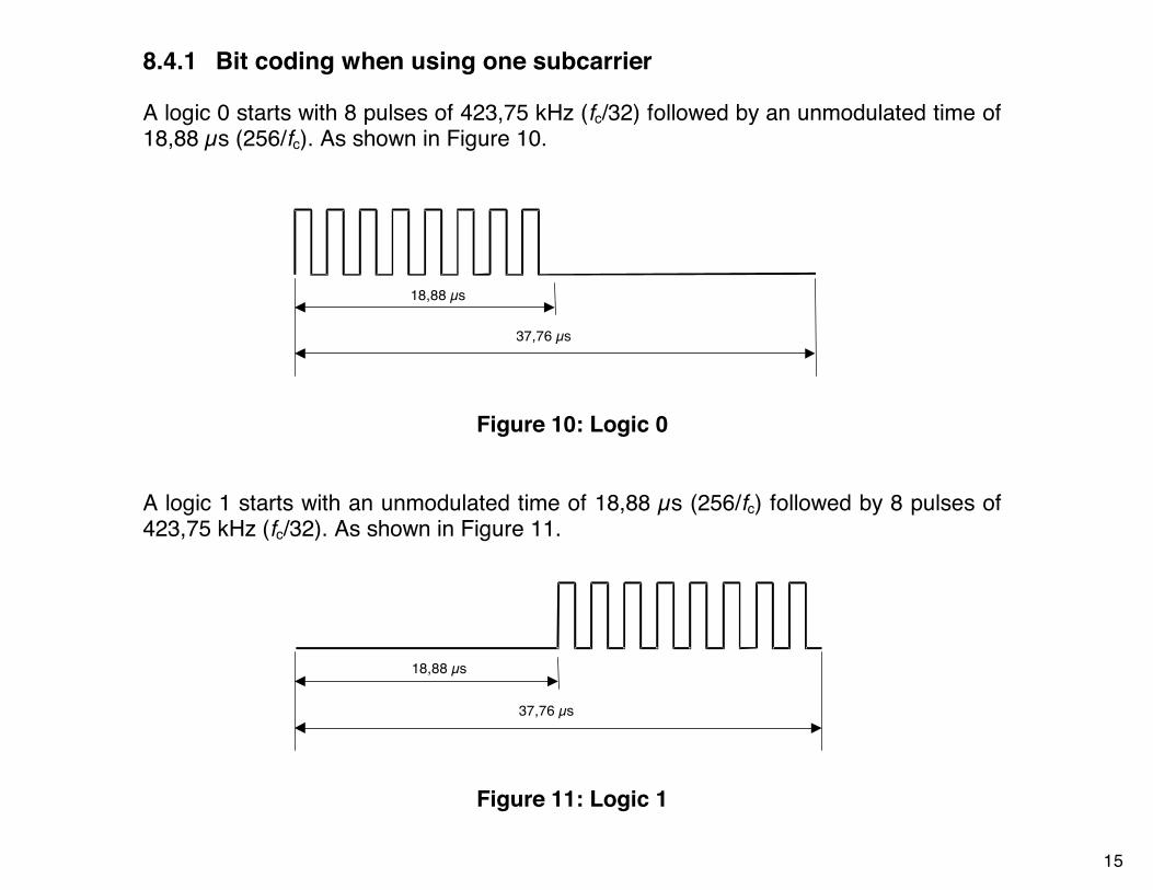
8.4.1 Bit coding when using one subcarrier
A logic 0 starts with 8 pulses of 423,75 kHz (fc/32) followed by an unmodulated time of18,88 µs (256/fc). As shown in Figure 10.
Figure 10: Logic 0
A logic 1 starts with an unmodulated time of 18,88 µs (256/fc) followed by 8 pulses of423,75 kHz (fc/32). As shown in Figure 11.
Figure 11: Logic 1
8.4.2 Bit coding when using two subcarriers
A logic 0 starts with 8 pulses of 423,75 kHz (fc/32) followed by 9 pulses of 484,28 kHz(fc/28). As shown in Figure 12.
Figure 12: Logic 0
A logic 1 starts with 9 pulses of 484,28 kHz (fc/28) followed by 8 pulses of 423,75 kHz(fc/32). As shown in Figure 13.
37,76 µs
18,88 µs
37,76 µs
18,88 µs
37,46 µs
18,88 µs
15

Passive tags are mostly meant to identify inexpensive objects, and must thus, submit to an economic asceticism that eschews such luxuries. Conventional batteries are far toobulky and expensive to be considered. A conventional radio transmitter or receiver, with the complex and expensive oscillators, mixers, and synthesizers is out of the question.Only inexpensive, low-speed circuitry and simple logic are permitted to us if the tag is to be powered by the pittance of microwatts available at several meters distance from areader. Instead of a proper transmitter, a switch to change the impedance presented to an antenna must suffice. A single IC is usually the only electrical &rar component to beplaced on the tag, and thus, this circuit must be a custom design solely for its specialized application. The expense of creating such an application-specific integrated circuit(ASIC) implies that only large volume usage can provide an economic return to the company responsible for it.
Between these extremes lie semipassive tags, possessed of a battery but bereft of a radio. To date, such tags have typically been constructed for specialized applications withmoderate volumes, such as auto tolling, and use fairly conventional fabrication and design approaches, with special attention to duty cycle just as for active tags.
A greatly simplified diagram of the electrical constituents of a passive tag is depicted in Figure 5.1. The radio signal at around 900 MHz from the reader is converted by theantenna into an alternating current, from which the tag must extract both power and information. The tag must then interpret the resulting data, possibly requiring writing data tononvolatile memory, and modulate the load presented to the antenna in order to change the backscattered signal returning to the reader.
In what follows, we shall examine a few of the special challenges of designing and manufacturing a passive UHF tag:
How is power to be extracted from the high-frequency radio signal?How can we simultaneously acquire whatever data the reader has sent?How do we send back information to the reader?How is the resulting chip designed and fabricated?How is a completed tag assembled from the chip and other parts?
RF to DC
To operate, a tag IC needs not just power, but direct-current (DC) power: a source of voltage that is roughly constant in time, of magnitude from 1 to 3 V depending on the type oftransistors used in the circuitry, and capable of supplying a few tens of microamps of current. The tag needs to get this DC power from an incoming RF signal whose polaritychanges about 900 million times per second, and with the proviso that at a few meters from the reader, a small tag antenna provides an open-circuit voltage of only about 0.1–0.3 V.
To change alternating (AC) voltages to DC, we need an electrical component that treats positive and negative polarities differently: a diode. The left side of Figure 5.2 shows theidealized version of a diode: a component that allows electrical current to flow only in one direction. The right side of the figure shows a more realistic view of a diode’scharacteristics: in the allowed (forward) direction current turns on slowly until some turn-on voltage is reached, thereafter increasing more rapidly. In the blocked (reverse)direction, a small leakage current flows, increasing as reverse voltage is increased.
Page 1 of 26http://rfid.net/basics/passive/137-uhf-rfid-tags?tmpl=component&print=1&layout=default&page=16

9/20/2012 12:38 PMPassive UHF RFID Tags
When the RF input becomes positive, the first diode turns off and the second (output) diode turns on (Figure 5.8). The charge that was collected on the input capacitor travelsthrough the output diode to the output capacitor. The peak voltage that can be achieved is found by adding the voltage across the input capacitor, which we found above, to thepeak positive RF voltage and subtracting the turn-on voltage of the output diode:
In the limit where the turn-on voltage can be ignored (e.g. when the input voltage is very large), the output DC voltage is double the peak voltage of the RF signal, from which factthe circuit derives its name. The actual output voltage depends on the amount of current drawn out of the storage capacitor during each cycle, that is on the value of the loadresistance (not shown here).
To produce higher output voltages, we can provide additional stages of multiplication to produce a Dickson charge pump. A two-stage configuration is shown in Figure 5.9; in thecase of ideal diodes with negligible turn-on voltage, the output would be four times larger than the peak RF input voltage. In general, for N stages we find:
9/20/2012 12:38 PMPassive UHF RFID Tags
A reasonable approach to estimating the number of stages is to extract an equivalent resistance from the load, given the total power calculated above:
where the input voltage is adjusted to produce the requisite load voltage from equation (5.7). Roughly speaking, the largest resistance that can be matched to the antenna is Q2times larger than the radiation resistance of the antenna. For a typical dipole-type antenna, this value is 10–50 Ω, so the largest equivalent resistance that can be optimallymatched is around 5 kΩ, assuming the limits on matching mentioned above. (Higher values can be used but at some sacrifice in bandwidth.) We can thus, adjust the number ofstages in the charge pump to provide about the right equivalent resistance for the value of Q we expect to achieve in matching.
Several weaker but non-negligible effects are important in arriving at a final design. The area of the diodes has a weak (logarithmic) effect on the turn-on voltage and thus on theefficiency, so one is tempted to make the diodes large. However, the diode capacitance grows linearly with the diode area, and since the equivalent resistance of the chargepump is fixed (by the power and voltage targets, as described above), as the diodes are made larger the capacitor starts to draw a substantial reactive current. The capacitanceis also voltage dependent (increasing noticeably as the diodes are turned on), and the variation in capacitance degrades the performance of the matching network, particularlyfor narrow band, high-Q networks. A charge pump with more stages has smaller capacitance variations because the peak voltage across each diode is closer to the turn-on
17
9/20/2012 12:38 PMPassive UHF RFID Tags
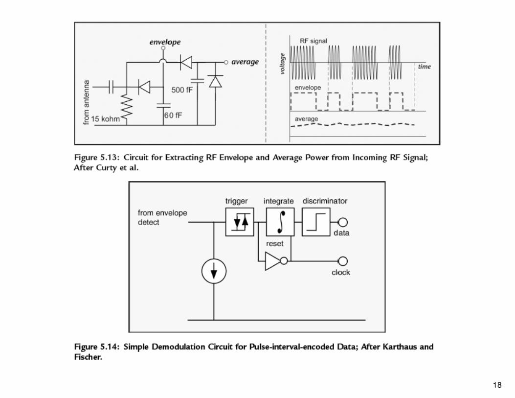
Once we have obtained a low-frequency voltage proportional to the RF power, we need to extract information from it. If the data is, for example, PIE coded, what we need tofigure out is how long the signal remains high between pulses: a long RF-high period represents a binary-1 and a short RF-high period represents a binary-0 (see for exampleFigure 3.7). One simple approach is shown in Figure 5.14. The output of the envelope-detect circuit is directed to a trigger circuit, with an optional current source or otherprovisions to set the threshold for the trigger. The trigger thus changes state at the beginning of an RF-on pulse, and resets an integrator, which then starts accumulating chargewhile the voltage is high. The output of the integrator grows linearly with time as long as a signal is applied to its input; on the next rising edge of the RF signal, the integratoroutput is large if the power was high for a long time, or smaller if the RF-high time was short. That output is applied to a discriminator, which then outputs a 1 or 0 depending onthe duration of the RF-high period, just as desired.
Recall that a radio receiver typically includes filtering to select the desired channel, and minimize noise and interference from other transmitters. A passive tag has no suchluxurious amenities. Since there is no local RF oscillator or mixer, there is no conversion operation to allow for channel filtering: all received signals at any RF frequency areconverted to baseband by the charge pump. The tag antennas provide some frequency selectivity but will generally cover at least the 902–928 MHz ISM band for United Statesoperation. Thus, any transmission in this band, including not only other RFID readers but cordless phones, wireless networks, cell phones and cell basestations, alarm systems,badly grounded spark plug wires, and any other nearby RF radiators all blast right into the IC’s receiver.
Talking Back
Passive tags use modulation of the power scattered by the tag antenna to reply to the reader. In our earlier discussions of backscatter modulation, we imagined a very simplescheme in which the IC simply interrupts current flow through the antenna to modulate the scattered power (see for example Figure 3.15). Let’s take a closer look at how onemight modulate the behavior of the antenna and what the consequences are. The three questions we need to address are:
How much scattered power can we send back to the reader?What effect do we have on the power absorbed by the (IC) load?How hard is it to implement a given scheme?
Let us first examine the limiting cases of the loads that can be presented to the antenna. These are shown schematically in Figure 5.15. Note that in this and subsequentdiagrams, we show an antenna connected to a ground node, which is defined to be at zero voltage. In practice, most tag antennas are symmetric and there is no easy way todefine a true “zero” voltage, but the principles are the same, and it is much easier to discuss the problem in this single-ended configuration, rather than the actual balanced ordifferential connection.
In normal operation, we shall assume that the IC is matched to the antenna: that is, the antenna and IC have been adjusted so that the largest possible power is delivered to theIC. We shall momentarily specify in more detail what this implies about the behavior of the system.
18

Once we have obtained a low-frequency voltage proportional to the RF power, we need to extract information from it. If the data is, for example, PIE coded, what we need tofigure out is how long the signal remains high between pulses: a long RF-high period represents a binary-1 and a short RF-high period represents a binary-0 (see for exampleFigure 3.7). One simple approach is shown in Figure 5.14. The output of the envelope-detect circuit is directed to a trigger circuit, with an optional current source or otherprovisions to set the threshold for the trigger. The trigger thus changes state at the beginning of an RF-on pulse, and resets an integrator, which then starts accumulating chargewhile the voltage is high. The output of the integrator grows linearly with time as long as a signal is applied to its input; on the next rising edge of the RF signal, the integratoroutput is large if the power was high for a long time, or smaller if the RF-high time was short. That output is applied to a discriminator, which then outputs a 1 or 0 depending onthe duration of the RF-high period, just as desired.
Recall that a radio receiver typically includes filtering to select the desired channel, and minimize noise and interference from other transmitters. A passive tag has no suchluxurious amenities. Since there is no local RF oscillator or mixer, there is no conversion operation to allow for channel filtering: all received signals at any RF frequency areconverted to baseband by the charge pump. The tag antennas provide some frequency selectivity but will generally cover at least the 902–928 MHz ISM band for United Statesoperation. Thus, any transmission in this band, including not only other RFID readers but cordless phones, wireless networks, cell phones and cell basestations, alarm systems,badly grounded spark plug wires, and any other nearby RF radiators all blast right into the IC’s receiver.
Talking Back
Passive tags use modulation of the power scattered by the tag antenna to reply to the reader. In our earlier discussions of backscatter modulation, we imagined a very simplescheme in which the IC simply interrupts current flow through the antenna to modulate the scattered power (see for example Figure 3.15). Let’s take a closer look at how onemight modulate the behavior of the antenna and what the consequences are. The three questions we need to address are:
How much scattered power can we send back to the reader?What effect do we have on the power absorbed by the (IC) load?How hard is it to implement a given scheme?
Let us first examine the limiting cases of the loads that can be presented to the antenna. These are shown schematically in Figure 5.15. Note that in this and subsequentdiagrams, we show an antenna connected to a ground node, which is defined to be at zero voltage. In practice, most tag antennas are symmetric and there is no easy way todefine a true “zero” voltage, but the principles are the same, and it is much easier to discuss the problem in this single-ended configuration, rather than the actual balanced ordifferential connection.
In normal operation, we shall assume that the IC is matched to the antenna: that is, the antenna and IC have been adjusted so that the largest possible power is delivered to theIC. We shall momentarily specify in more detail what this implies about the behavior of the system.
9/20/2012 12:38 PMPassive UHF RFID Tags
When an open circuit is presented to the antenna, the path to ground is blocked and no current flows in the antenna; since there is no current flowing, no power is radiated(backscattered) in this state. (Real antennas are not quite so simple and do scatter some power even when they are presented with an open circuit load, and real antennadesigns don’t quite correspond to the configuration shown here.)
When a short circuit is presented to the antenna, current flows readily to ground without encountering any resistance or creating any voltage. It may be inferred that, in this case,a large antenna current flows and substantial scattered power results.
In order to examine the use of these three states for modulation in a quantitative fashion, we need to construct an equivalent circuit for an antenna. We’ll use the very simplifiedcircuit in Figure 5.16. The antenna is represented by a voltage source Vant, arising from the impinging RF electric field from the reader, and a radiation resistance Rrad, sonamed because it arises not from the electrical resistance of the metal of which the antenna is constructed but from the power lost in the scattered waves that result whencurrent flows in the antenna. The antenna current must flow also through a load consisting of the (constant) load resistance due to the IC’s power supply (the charge pumps wediscussed in Sections 5.2 and 5.3 above), with provisions for opening or closing switches to present either an open or a short to the antenna.
The power delivered to the radiation resistance (and thus scattered back into the world) is proportional to the product of the square of the current and the resistance, like anyother resistor. When the switches are in the default configuration Figure shown, the same current must flow through the load resistor. The total current is readily found fromOhm’s law (see Appendix 3):
When the load resistance is very small compared to the radiation resistance, there isn’t much voltage across the load and little power is delivered to the load. When the loadresistance is much larger than the radiation resistance, all the voltage appears across the load, but little current flows, so again not much power is delivered to the load. It is easyto show that the optimum power transfer—the matched condition—occurs when the values of the source and load resistance are equal. This is the state to which all our previouscalculations of the power available from an antenna referred. Note that as a consequence, in the matched condition, the power dissipated in the load is equal to the powerdissipated in the radiation resistance—that is, a matched antenna scatters as much power as it receives. Let us denote this power Pav, the available power. This is the baselinebackscattered signal of the unmodulated, matched antenna. We must now examine how this signal changes when we change the load.
19

assumes the availability of reference voltages for PMOS and NMOS devices that ensure that a certain fixed reference current per micron of gate width flows through transistorsbiased with the cited voltages. The reference voltages are created by tapping off the gate voltage of similar NMOS and PMOS transistors adjusted in a current-mirrorconfiguration to keep their output current constant.
The circuit alternates between the two states depicted in Figure 5.22. In state (a) the output is high. The capacitor is positive, thus holding T2 off and T3 on. The output voltage isalso fed back to T1, which connects the NMOS reference transistor to the negative supply voltage. This reference current discharges the positive voltage stored on capacitor C.When the capacitor voltages falls sufficiently, the circuit switches to state (b). T2 turns on and T3 turns off; the output voltage is pulled negative, and fed back to turn T1 off andT4 on. The NMOS reference current terminates, and the PMOS reference current charges the capacitor. Thus, the oscillation frequency is set by the capacitor size, the transistorthreshold voltages, and the reference current.
Note that operation of this circuit requires that five transistors operate in series from the difference between +V and −V. This circuit was designed for implementation in a low-threshold-voltage, silicon-on-insulator (SOI) process. A conventional field-effect transistor is manufactured by placing a gate electrode in close proximity to a doped region in abulk silicon wafer, separated by a thin oxide insulator. The transistor is turned off by adjusting the voltage on the gate to repel the channel carriers (electrons or holes), but somecarriers are able to make their way through the underlying silicon from one side of the transistor to the other, contributing to leakage current. In an SOI process, the channel isconstructed on top of an insulating layer, so that leakage current in the off state (subthreshold leakage) is reduced, and devices with very small threshold voltages can be used.The cost of SOI processing is generally higher than that of conventional CMOS. In a standard process, the need to supply five threshold voltages in series, which requires theavailability of a high supply voltage, will likely limit read range, so this circuit might need to be redesigned for conventional implementation.
Tag IC Overall Design Challenges
Now that we’ve touched on the problems presented by the interface to the physical world, let us turn our attention to the logic, memory, and supporting systems that make thetag responsive to its environment. A rough functional layout of a typical passive tag IC is depicted in Figure 5.23. Around half the chip area is taken up by the logic needed toimplement the relevant protocol: about 50 000 transistors for an 18000-6C (EPCglobal Class 1 Generation 2) IC.
We’ve looked at the key RF-related challenges in Sections 5.2–5.4 above. The remainder of the chip operates at baseband frequencies and is generally similar to conventionalmixed-signal design. However, there are some special challenges peculiar to the RFID world.
The first challenge is, of course, that of cost. The cost of a chip is dominated by its size if yield is reasonably good. Modern IC manufacturing facilities use 200-mm- or 300-mm-diameter wafers. A standard 200-mm-diameter silicon wafer offers a useful area of about 30 000 square millimeters. (This is a bit less than the total surface area: the regionwithin about 3 mm of the wafer edge is usually not useful for processing.) If a single IC has a useful area of around 1 mm2, we can get about 22 000 chips from a waferassuming that 90% of the chips are good (that is, the yield is 90%). In small volumes, it costs about $1000 to purchase a processed wafer, so the cost of these ICs would beroughly $0.05 per chip. The use of 300-mm wafers increases the initial cost for masks, but in high volume the ongoing cost is reduced by 30–40% vs. 200-mm wafer. The actualnumbers are influenced by such commercial issues as volume pricing—I don’t pay $1000/wafer if I buy several hundred wafers—but it should be apparent that at 1 squaremillimeter, the chip cost is a substantial fraction of the $0.05 tag cost goal promulgated by such organizations as EPCglobal. It is imperative to keep the chip as small as possibleto minimize IC cost.
Traditionally, the size of digital ICs has been strongly influenced by scaling: the reduction in the size of transistors due to improvements in lithography and processing, whichresults in a reduction in the size of the chip for the same number of transistors. Technologies are usually named for the smallest feature size used in the process: for example, atypical high-speed fabrication process might make use of an 0.13-μm line to form the transistor gate, and would generally be referred to as an 0.13-μm process. For many years,scaling the size of the transistor down also resulted in reduced power consumption per transistor. However, there are some obstacles to achieving the benefits of scaling in RFIDchips over the next several years. First of all, the most advanced process technology is always expensive. It is much cheaper to purchase masks and wafers for 0.18-μmprocessing than for 0.13-μm processing. Secondly, the benefits of scaling are decreasing as fundamental limits in process technology are reached. For example, silicon dioxidefilms, critical for forming MOS transistors, have reached thicknesses equivalent to only about 3 molecular layers and can’t be reduced much more. Efforts to replace silicondioxide in this role have so far been unfruitful. Because of leakage through these thin oxide films, power consumption in very small devices is also not as small as one mighthave expected from extrapolation from older technologies.
A substantial fraction of an RFID IC consists of analog functional blocks: RF rectifiers for power supplies, capacitors for energy storage, and circuitry for decoding andmodulation. The size of analog blocks doesn’t necessarily change just because the minimum feature size is reduced. For example, the area required for a storage capacitor isset by the total power consumption of all the chip features, so if power consumption doesn’t go down, the capacitor must remain the same size. A diode’s size is set by theparasitic resistance and capacitance associated with it, which determine the frequency it can operate at and the impact it has on the antenna match. A modulation capacitor’ssize is set by the characteristics of the antenna and the modulation efficiency we seek to achieve. Protection circuitry requirements are determined by the largest voltage the tagexpects to see, not by the smallest voltage its transistors could operate at. While in general, the size of the analog blocks can shrink if the power consumption of the logic theysupport is reduced, analog functions usually don’t scale down in size nearly as readily as the corresponding digital circuitry.
So, we can’t expect scaling alone to magically reduce IC costs. It is also important to exploit every possible measure to reduce size and power consumption of the logic blocks.Automatic routing of wires between transistors is fast and convenient, but clever human designers can squeeze space out of the design by (laborious) manual optimization.Power consumption in the logic circuitry can be reduced by operating the devices near the threshold voltage (the minimum voltage to turn the transistors on), but thresholdvoltage differs from one chip to another due to variations in manufacturing and due to temperature variations in operation. It is possible to use onboard nonvolatile storage toadapt the operation of each chip to its conditions. Such threshold adjustment techniques may also allow the use of MOSFETs instead of junction diodes or expensive Schottkydiodes for rectification.
Finally, a tag IC has a number of logic blocks, all running from a very high-impedance antenna (that is, an antenna that has a hard time supplying much current). Each time alogic gate switches its state, a transient current flows from the local power supply connection. If the local supply voltage fluctuates as a consequence—that is, if decoupling isinsufficient—the change could be interpreted by a nearby gate as a logical input, leading to errors in operation of the circuit. The challenge of properly isolating the individualgates and the segments of the circuit, is much larger than in conventional circuit design, where power at a reasonably fixed voltage is available from a battery or power supply.
Packaging: No Small Matter
So far we’ve focused on the electrical guts of a passive tag, but the physical construction is also of great importance. The IC must be connected either to an intermediate strap or
20
iClass SecurityiClass Card Cloning using an RW300 Reader/Writer
Hacking RFID for Fun – www.proxclone.com Page 1
Background The HID iClass family of 13.56 Mhz Contactless readers and cards was introduced over a decade ago with the primary goal of eliminating some of the security concerns that existed with the older 125Khz Proximity technology. The state-of-the-art iClass technology supported new features such as mutual authentication and Triple DES encryption to improve security and reduce the possibility of card duplication.
The contactless cards themselves utilize an embedded chip technology called "PicoPass" from a French company by the name of Inside Secure http://www.insidesecure.com/ . These chips basically consist of a small EEPROM memory and a simple state machine controller that is used to interact with a card reader using the ISO 14443B and ISO 15693 protocols.
All data stored on iClass cards is secured by Authentication Keys. A Key is basically a password used to protect data from being read or changed without authorization. The iClass cards and readers use 64-bit keys (56 key bits plus 8 parity bits). One authentication key is used to protect each of the card’s Application Areas. Two encryption keys are used to support TDES encryption of the transferred data.
Since its introduction, numerous articles have been written by HID and other security industry experts who have all described the technology as "Extremely Secure" and "Difficult to Clone". Those kinds of words are usually interpreted by the hacking community as an open challenge to explore the technology and to identify and exploit any vulnerabilities that are found to exist. As a result, within the last year at least two excellent papers have been written that describe how to exploit the iClass technology. These papers discuss various methods of recovering the HID's secret authentication and encryption keys that are used with HID's "Standard Security" mode of operation and which are globally installed in all of their readers. The extraction of these keys leads to the ability to duplicate any of the "Standard Security" iClass cards that exist in the market today. The two previously published papers can be found here:
“Heart of Darkness- exploring the uncharted backwaters of HID iClass security “ http://www.openpcd.org/HID_iClass_demystified
“Exposing iClass Key Diversification” http://www.usenix.org/events/woot11/tech/final_files/Garcia.pdf
Project Goals Since I am a hardware engineer by trade with no C/C++ programming experience and no C/C++ development tools I was unable to capitalize on the source code provided in the above links. As a result, my introduction to the complex world of iClass technology hacking had to begin from scratch. My primary goals were as follows:
• Extract the Authentication and Encryption keys from an iClass reader using only the PIC PicKit2 debugger tool and any other custom tools that I could create on my own.
21

http://www.openpcd.org/HID_iClass_demystified27TH CHAOS COMMUNICATION CONGRESS IN BERLIN, DECEMBER 2010 1
Heart of Darkness - exploring the unchartedbackwaters of HID iCLASSTM security
Milosch Meriac, [email protected]
Abstract—This paper provides detailed information oniCLASSTMreader and key security. It explains the security prob-lems found without revealing the extracted secret keys (DESauthentication Key and the 3DES data encryption key foriCLASSTMStandard Security cards).
The chosen approach of not releasing the encryption andauthentication keys gives iCLASS vendors and customers animportant headstart to update readers and cards to High Securitymode in order to stop attackers from forging, reading and cloningiCLASS Standard Security cards.
This paper also explains, how Standard Security and HighSecurity keys were extracted from a RW400 reader withoutleaving visible traces.
I. INTRODUCTION
Hunters for gold or pursuers of fame,they all had gone out on that stream,bearing the sword, and often the torch ...
– Joseph Conrad: Heart of Darkness
Most existing RFID card systems like Mifare Classic1
and Legic Prime2 are already well researched. The lack ofsecurity found in these systems increased my attention onother undocumented RFID systems.
This year my interest was caught by HID’s iCLASS system.The iCLASS protocol is not documented publicly and saleschannels for cards, keys, readers and writers seem to be tightlycontrolled.
After some intitial research I discovered that CP400 pro-grammers for iCLASS cards are not available on sale, but areonly available for leasing under tight contracts and high costs.Non-configured, non-programmed iCLASS cards are no longeravailable from HID - this made me curious enough to ordersome second hand RW400 writers from Ebay and some cards.Interestingly I was able to buy unprogrammed cards, whichallowed me to do some research on the protocol side as well.
Chapter II gives a brief overview of iCLASS Security.The physical reader security is evaluated in chapter III andshows how the lack of attention to CPU data sheets leads tovulnerabilities that result in leaking of firmware images andkey material.
This paper is meant as supplementary information to my joint talk Analyzinga modern cryptographic RFID system with Henryk Plötz at the 27th ChaosCommunication Congress in Berlin, December 2010. Please visit http://openpcd.org/HID_iClass_demystified for updated information.
124C3 - Mifare Classic, Little security despite obscurity:http://events.ccc.de/congress/2007/Fahrplan/events/2378.en.html
226C3 - Legic Prime, Obscurity in Depth:http://events.ccc.de/congress/2009/Fahrplan/events/3709.en.html
Detailed suggestions to improve system security can befound in chapter IX.
The protocol security aspects of the iCLASS RFID protocolwill be presented separately at the public 27C3 talk and thuswill not be duplicated here in this paper.
II. ICLASS SECURITY
Do you want the convenienceof receiving preprogrammed cardsthat are ready for use? No problem -trust HID to manage your keys! -
– N. Cummings, HID: iCLASS Levels of Security
iCLASS cards come in two flavors: “Standard Security”and “High Security”. In Standard Security mode the customerbuys preprogrammed cards from HID that contain a uniquecombination of card number and facility ID.
Each individual card is initialized with a diversified key. Thereader key is hashed with the card serial number to create aunique key3.
When a card is presented to a reader, the card ID is read, thecard key is diversified and the card authentication process isstarted based on the diversified per-card key. Every successfulcard read results in a “beep-n-blink” of the reader and atransmission of the data payload to the backend system.
A. Standard SecurityStandard Security mode means that two common secret keys
are shared across all HID readers in that Mode. The suppliedcards contain a unique combination of a card ID and a per-facility ID. A reader in a Standard Security mode will thereforesuccessfully authenticate all Standard Security iCLASS cardsand will send the stored card ID and facility ID, usually inWiegand format, to the upstream system.
The upstream system decides based on the transmitted dataif the card is part of the system and determines the accesslevel.
B. High SecurityHigh Security essentially means, that each system uses
a system specific key. This system specific key is alreadyused during authentication phase. As authentication fails whenpresenting a Standard Security or High Security card fromanother High Security system, no “beep-n-blink” will occuron the reader.
3iCLASSTMLevels of Security: http://goo.gl/AUWOP
27TH CHAOS COMMUNICATION CONGRESS IN BERLIN, DECEMBER 2010 1
Heart of Darkness - exploring the unchartedbackwaters of HID iCLASSTM security
Milosch Meriac, [email protected]
Abstract—This paper provides detailed information oniCLASSTMreader and key security. It explains the security prob-lems found without revealing the extracted secret keys (DESauthentication Key and the 3DES data encryption key foriCLASSTMStandard Security cards).
The chosen approach of not releasing the encryption andauthentication keys gives iCLASS vendors and customers animportant headstart to update readers and cards to High Securitymode in order to stop attackers from forging, reading and cloningiCLASS Standard Security cards.
This paper also explains, how Standard Security and HighSecurity keys were extracted from a RW400 reader withoutleaving visible traces.
I. INTRODUCTION
Hunters for gold or pursuers of fame,they all had gone out on that stream,bearing the sword, and often the torch ...
– Joseph Conrad: Heart of Darkness
Most existing RFID card systems like Mifare Classic1
and Legic Prime2 are already well researched. The lack ofsecurity found in these systems increased my attention onother undocumented RFID systems.
This year my interest was caught by HID’s iCLASS system.The iCLASS protocol is not documented publicly and saleschannels for cards, keys, readers and writers seem to be tightlycontrolled.
After some intitial research I discovered that CP400 pro-grammers for iCLASS cards are not available on sale, but areonly available for leasing under tight contracts and high costs.Non-configured, non-programmed iCLASS cards are no longeravailable from HID - this made me curious enough to ordersome second hand RW400 writers from Ebay and some cards.Interestingly I was able to buy unprogrammed cards, whichallowed me to do some research on the protocol side as well.
Chapter II gives a brief overview of iCLASS Security.The physical reader security is evaluated in chapter III andshows how the lack of attention to CPU data sheets leads tovulnerabilities that result in leaking of firmware images andkey material.
This paper is meant as supplementary information to my joint talk Analyzinga modern cryptographic RFID system with Henryk Plötz at the 27th ChaosCommunication Congress in Berlin, December 2010. Please visit http://openpcd.org/HID_iClass_demystified for updated information.
124C3 - Mifare Classic, Little security despite obscurity:http://events.ccc.de/congress/2007/Fahrplan/events/2378.en.html
226C3 - Legic Prime, Obscurity in Depth:http://events.ccc.de/congress/2009/Fahrplan/events/3709.en.html
Detailed suggestions to improve system security can befound in chapter IX.
The protocol security aspects of the iCLASS RFID protocolwill be presented separately at the public 27C3 talk and thuswill not be duplicated here in this paper.
II. ICLASS SECURITY
Do you want the convenienceof receiving preprogrammed cardsthat are ready for use? No problem -trust HID to manage your keys! -
– N. Cummings, HID: iCLASS Levels of Security
iCLASS cards come in two flavors: “Standard Security”and “High Security”. In Standard Security mode the customerbuys preprogrammed cards from HID that contain a uniquecombination of card number and facility ID.
Each individual card is initialized with a diversified key. Thereader key is hashed with the card serial number to create aunique key3.
When a card is presented to a reader, the card ID is read, thecard key is diversified and the card authentication process isstarted based on the diversified per-card key. Every successfulcard read results in a “beep-n-blink” of the reader and atransmission of the data payload to the backend system.
A. Standard SecurityStandard Security mode means that two common secret keys
are shared across all HID readers in that Mode. The suppliedcards contain a unique combination of a card ID and a per-facility ID. A reader in a Standard Security mode will thereforesuccessfully authenticate all Standard Security iCLASS cardsand will send the stored card ID and facility ID, usually inWiegand format, to the upstream system.
The upstream system decides based on the transmitted dataif the card is part of the system and determines the accesslevel.
B. High SecurityHigh Security essentially means, that each system uses
a system specific key. This system specific key is alreadyused during authentication phase. As authentication fails whenpresenting a Standard Security or High Security card fromanother High Security system, no “beep-n-blink” will occuron the reader.
3iCLASSTMLevels of Security: http://goo.gl/AUWOP
HEART OF DARKNESS - EXPLORING THE UNCHARTED BACKWATERS OF HID ICLASSTM
SECURITY 6
Fig. 10. ContactlessDemoVC.exe demo application from the OMNIKEYSynchronous API SDK - shows the succesful read of data from inside theprotected HID Access Control Application.
To access iCLASS cards, the “OMNIKEY Synchronous APIfor Windows” 13 needs to be installed additionally to the devicedriver software.
B. Let’s talk APDUs, Baby
For starters, the application ContactlessDemoVC.exe in theSynchronous API SDK provides simple means to communicatewith the x321 RFID writer (Fig. 10).
Let us have a quick look on how the APDU14 communicationusing ContactlessDemoVC looks like (Table III). Each APDUrequest/reply-pair is seperated by a double line. The crossed-out authentication key is the reverse permuted eight byteauthentication key from Fig. 8 at offset 0x88. It not onlyallows full read authentication to the secured HID AccessControl Application, but also enables write access to this area(block 9 in this example).
C. Writing the HID Access Control Application
As can be seen in table III, write acess to the protectedHID Access Control Application is possible - contrary to thefollowing statement in the “Contactless Smart Card ReaderDeveloper Guide”:
“Note: OMNIKEY Contactless Smart Card readers does notallow WRITE access to the HID application (1st applicationon page 0). For READ access to the HID application, securedcommunication (available for firmware version 5.00 andgreater) is mandatory.”
The idea behind the secure communication mode to OM-NIKEY readers is that HID delivers these readers with theauthentication key installed. By establishing the secured com-munication with the reader the HID Access Control Applicationcan be read - presumably to allow applications like signing onto computers by using an iCLASSTMemployee card credential.
13OMNIKEY Synchronous API for Windows: http://goo.gl/uH71V14APDU: Application Protocol Data Units as defined in the OMNIKEY
Contactless Smart Card Readers Developer Guide (http://goo.gl/Itpqf)
TABLE IIIREADING AND WRITING THE PROTECTED HID ACCESS CONTROL
APPLICATION
select card 80A60000
9000 success
load key 808200F008XXXXXXXXXXXXXXXX
9000 success
authenticate 808800F0
9000 success
read block 6 80B0000600
030303030003E0179000 block 6 + success
read block 7 80B0000700
BC8793E20AF06F339000 block 7 + success
read block 8 80B0000800
2AD4C8211F9968719000 block 8 + success
read block 9 80B0000900
2AD4C8211F9968719000 block 9 + success
write block 9 80D60009080102030405060708
9000 success
read block 9 80B0000900
01020304050607089000 block 9 + success
The authentication for secure mode communication betweenreader and card is done both-ways using the 16 byte 3DESkeys KCUR (Custom Read Key) and KCUW (Custom WriteKey). One needs to sign a NDA with HID to receive these twokeys from HID. The control of these keys by HID limits thegroup of people with read access to the HID Access ControlApplication.
As HID probably never planned to reveal these access keysto customers and write support would be a serious threat toStandard Security cards (as explained later in chapter V), it’sonly natural to filter out write requests when using the pre-installed authentication key. On the opposite it is only naturalthat user-uploaded keys give full write support to the card.
Give a big hand to HID OMNIKEY for providing us withsuch a well designed, nice looking and widely available attacktoolkit for copying iCLASSTMcards.
V. COPYING ICLASS CARDS
— he cried out twice,a cry that was no more than a breath —’The horror! The horror!’
– Joseph Conrad: Heart of Darkness
One of the biggest don’ts in card security is to design a cardsecurity system which allows copying cards without forcing theattacker to use a card emulator. Out of no apparent reason thisimplementation flaw exists for HIDs iCLASS cards: Knowingthe authentication key results in beeing able to copy the cards- decrypting 3DES encrypted content is not necessary for that.
As the the Standard Security keys were extracted successfullyin the previous steps and write access is possible, copying of
HEART OF DARKNESS - EXPLORING THE UNCHARTED BACKWATERS OF HID ICLASSTM
SECURITY 8
TABLE IVCONFIGURATION CARD CONTENT
Block Encrypted Decrypted
00 4D 13 D1 00 F7 FF 12 E0
01 1F FF FF FF 7F 1F FF 3C
02 FC FF FF FF FF FF FF FF
03 FF FF FF FF FF FF FF FF
04 FF FF FF FF FF FF FF FF
05 FF FF FF FF FF FF FF FF
06 0C 00 00 01 00 00 BF 18
07 BF 01 FF FF FF FF FF FF
08 FF FF FF FF FF FF FF FF
09 FF FF FF FF FF FF FF FF
0A FF FF FF FF FF FF FF FF
0B FF FF FF FF FF FF FF FF
0C FF FF FF FF FF FF FF FF
0D C0 43 54 1E 77 14 FB DF 10 AC 40 BF 3F B5 9F 6E
0E 2E DE 81 0F 09 FD AE 12 7A 24 C5 33 68 FF 89 2E
0F 30 D4 BB 04 0B 5B 42 AA 61 31 4A D4 65 15 12 63
10 9E 80 2E 28 01 23 C7 A8 FF FF FF FF FF FF FF FF
11 9E 80 2E 28 01 23 C7 A8 FF FF FF FF FF FF FF FF
12 9E 80 2E 28 01 23 C7 A8 FF FF FF FF FF FF FF FF
13 03 00 00 00 00 00 00 1C
14 56 6B FA 14 34 4A 9F 48 15 10 AC 40 BF 3F B5 9F
15 21 55 85 E8 A2 CE 4B 8F 6E FF FF FF FF FF FF FF
16 9E 80 2E 28 01 23 C7 A8 FF FF FF FF FF FF FF FF
17 9E 80 2E 28 01 23 C7 A8 FF FF FF FF FF FF FF FF
18 9E 80 2E 28 01 23 C7 A8 FF FF FF FF FF FF FF FF
19 9E 80 2E 28 01 23 C7 A8 FF FF FF FF FF FF FF FF
1A 9E 80 2E 28 01 23 C7 A8 FF FF FF FF FF FF FF FF
1B 9E 80 2E 28 01 23 C7 A8 FF FF FF FF FF FF FF FF
1C 9E 80 2E 28 01 23 C7 A8 FF FF FF FF FF FF FF FF
1D 9E 80 2E 28 01 23 C7 A8 FF FF FF FF FF FF FF FF
1E 9E 80 2E 28 01 23 C7 A8 FF FF FF FF FF FF FF FF
1F 9E 80 2E 28 01 23 C7 A8 FF FF FF FF FF FF FF FF
With a second configuration card the key rolling can bedisabled and the reader acts as a read-only reader again. Fromthis point on the reader doesn’t accept standard security cardsany more - a very effective “Denial of Service” attack.
This default behavior of accepting configuration cards isundesirable as it allows attackers not only to highjack StandardSecurity reader infrastructures, but also to highjack cardspresented to this reader while the reader highjacking remainsundiscovered. I assume it’s difficult to recover from thatsituation as one probably needs the highjackers key to resetthe reader back to the original key or a new key.
A safe way to recover is to reflash the EEPROM contentback to the original content using the convenient externallyaccessible programming connector that was described earlierin chapter III and turning the reader back to Standard Securitymode that way.
A. Hotfix by switching to High Security mode
A quick countermeasure to this attack is to switch StandardSecurity installations to High Security Mode by using a con-figuration card. If the attacker doesn’t know the authenticationkey, simple configuration cards can’t be used any more totamper with the system.
VIII. OPEN QUESTIONS
It would be nice to clarify some of the remaining openquestions:
• Analyse the card dump of Standard Security cards withPIN codes set to check how the PIN number is secured.
• Analyse the card dump of Standard Security cards withstored biometric data to verify if the biometric data issigned with proper encryption or if the card can be copiedand the stored biometric template changed to the theattacker template.
• An interesting experiment could be to verify if High Se-curity Mode access cards with an unknown authenticationkey can be used to inject configuration card content usinga man-in-the-middle attack between the card and a systemreader. Using that approach, the attacked reader wouldrotate the unknown reader and card keys to a key knownby the attacker.A valid question is why the original 16 byte high securitykey is reduced to 8 bytes when written to the reader byusing a configuration card to switch to High Securitymode. This behavior can be observed by using the ISPdebug interface.To my understanding each card only uses a 8 byte keywhich is derieved from the reader authentication key usingat least the card hardware UID and the purse counter inblock 2. This effectively limits the incentive to sniff thecard authentication and offline breaking of the card keyvia brute force attack as only the individual card key canbe broken. This is not useful as the stored blocks aretransmitted over the air in clear text. Such a key wouldbe unusable for a copied card as the card ID would bedifferent - the sniffed key would be only usable with ancard emulator impersonating the same UID.But - using only 8 bytes reader authentication keys createsa large incentive to break one card key as in the next stepthe reader key can be broken due to the low key size of64 bits18. This could have been avoided as the card keyderivation could have used the full 16 byte High Securitykey and thus making such an attack impossible.
IX. RECOMMENDATIONS
• Standard Security Mode is dead19. Switch immediatelyto High Security by asking your local HID vendor forprogramming cards that will upgrade your StandardSecurity system to High Security and rotate your existingcards to the new keys at a trusted location only. Makesure that your vendor tells you the new High Securitykey.
• Encrypt the HID Access Control Application additionallywith a key only known to the backend system (position andUID dependent - AES, 3DES etc.). These encrypted blockswill be encrypted with the usual 3DES reader key beforestoring them on the card. When swiping the card they willbe decrypted with the reader key and transmitted to thebackend system via Wiegand Protocol. This effectively
18The 8 byte high security key doesn’t seem to be a straight permuted DESkey as the 8th byte is significant for a successful authentication.
19It’s not pinin,’ it’s passed on! This parrot is no more! It has ceased tobe! It’s expired and gone to meet its maker! This is a late parrot! It’s a stiff!Bereft of life, it rests in peace! If you hadn’t nailed him to the perch he wouldbe pushing up the daisies! Its metabolical processes are of interest only tohistorians! It’s hopped the twig! It’s shuffled off this mortal coil! It’s run downthe curtain and joined the choir invisible! This.... is an EX-PARROT! - fromMonty Python’s Pet Shop (Dead Parrot) Sketch.
22

dissipation, and small masses (10!15–10!17 kg), these devicesare well suited to such explorations. Their dimensions notonly make them susceptible to local forces, but also make itpossible to integrate and tightly couple them to a variety ofinteresting electronic structures, such as solid-state two-level systems (quantum bits, or qubits), that exhibit quan-tum mechanical coherence. In fact, the most-studied sys-tems, nanoresonators coupled to various superconductingqubits, are closely analogous to cavity quantum electrody-namics, although they are realized in a very different pa-rameter space.
Quantized nanomechanical resonatorsThe classical and quantum descriptions of a mechanical res-onator are very similar to those of the electromagnetic fieldin a dielectric cavity: The position- and time- dependent me-chanical displacement u(r,t) is the dynamical variable anal-ogous to the vector potential A(r, t). In each case, a waveequation constrained by boundary conditions gives rise to aspectrum of discrete modes. For sufficiently low excitationamplitudes, for which nonlinearities can be ignored, the en-ergy of each mode is quadratic in both the displacement andmomentum, and the system can be described as essentiallyindependent simple harmonic oscillators.
Spatially extended mechanical devices, such as thosein figure 1, possess a total of 3A modes of oscillation, where
A is the number of atoms in the structure. Knowing theamplitude and phase of all the mechanical modes is equiv-alent to having complete knowledge of the position and mo-mentum of every atom in the device. Continuum mechan-ics, with bulk parameters such as density and Young’smodulus, provides an excellent description of the modestructure and the classical dynamics, because the wave-lengths (100 nm–10 mm) of the lowest-lying vibrationalmodes are long compared to the interatomic spacing.
It is natural to make the distinction between nano-mechanical modes and phonons: The former are low-frequency, long-wavelength modes strongly affected by theboundary conditions of the nanodevice, whereas the latterare vibrational modes with wavelengths much smallerthan typical device dimensions. Phonons are relatively un-affected by the geometry of the resonator and, except indevices such as nanotubes that approach atomic dimen-sions, are essentially identical in nature to phonons in aninfinite medium.
It is an assumption that quantum mechanics shouldeven apply for such a large, distributed mechanical struc-ture. Setting that concern aside for the moment, one canfollow the standard quantum mechanical protocol to es-tablish that the energy of each mode is quantized:E " \w(N # 1/2), where N " 0, 1, 2, . . . is the occupation fac-tor of the mechanical mode of angular frequency w. The
http://www.physicstoday.org July 2005 Physics Today 37
2 mm
a
c
e
b
d
f
Source Drain
Gate
W
dz
Figure 1. Nanoelectro-mechanical devices. (a) A 20-MHz nanome-chanical resonator ca-pacitively coupled to asingle-electron transistor(Keith Schwab, Labora-tory for Physical Sci-ences).11 (b) An ultrasen-sitive magnetic forcedetector that has beenused to detect a singleelectron spin (DanRugar, IBM).3 (c) A tor-sional resonator used tostudy Casimir forces andlook for possible correc-tions to Newtonian grav-itation at short lengthscales (Ricardo Decca,Indiana University–Purdue University Indi-anapolis). (d) A paramet-ric radio-frequency me-chanical amplifier thatprovides a thousandfoldboost of signal displace-ments at 17 MHz(Michael Roukes, Cal-tech). (e) A 116-MHznanomechanical res-onator coupled to a single-electron transistor(Andrew Cleland, Uni-versity of California,Santa Barbara).10
(f) A tunable carbonnanotube resonator op-erating at 3–300 MHz (Paul McEuen, CornellUniversity).14
Downloaded 05 Sep 2012 to 128.59.145.17. Redistribution subject to AIP license or copyright; see http://www.physicstoday.org/about_us/terms
Next week…
23