Rfi blC tiReconfigurable Computing -...
25
R fi bl C ti Reconfigurable Computing Prof. Dr. Christophe Bobda University of Potsdam Institute for Computer Science Ch i f C t E i i ‹Nr.› C. Bobda, C.R.K. Prasad © Chair for Computer Engineering
Transcript of Rfi blC tiReconfigurable Computing -...
R fi bl C tiReconfigurable Computing
Prof. Dr. Christophe BobdapUniversity of Potsdam
Institute for Computer ScienceCh i f C t E i i
‹Nr.› C. Bobda, C.R.K. Prasad©
Chair for Computer Engineering

Chapter 2D i d I t tiDesign and Integration
2© Christophe Bobda

Agenda
1. In System Integration2 Design Flo2. Design Flow
3© Christophe Bobda
In System Integrationy g
4© Christophe Bobda

1. Rapid Prototyping
● Reconfigurable devices (RD) are● usually used in three different ways:● usually used in three different ways:
1. Rapid Prototyping: The RD is used as emulator for a circuit to be producedemulator for a circuit to be produced later as ASIC. The emulation process allows for testing the correctness of the i it ti d l ti APTIX S t E lcircuit, sometimes under real operating
conditions before production.APTIX System Explorer
The APTIX-System Explorer and the ITALTEL Flexbench systems are two examples of emulation platforms.examples of emulation platforms.
ITALTEL FLEXBENCH
5© Christophe Bobda
ITALTEL FLEXBENCH

1. Non Frequent reconfiguration
2. Non-frequently reconfigurable systems: The RD is used assystems: The RD is used as application specific device similar to ASIC. However the possibility of upgrading the system by means ofupgrading the system by means of reconfiguration is given.
Such systems are used as
The Nallatech BenADIC
Such systems are used as prototyping platform, but can be used as running environment as well.well.
Examples are:The RABBIT System, the celoxicaThe RABBIT System, the celoxica RC100, RC200, RC300, the Nallatech BenADIC. The Celoxica RC200
6© Christophe Bobda

1. Frequent reconfiguration
3. Frequently reconfigurable systems: Usually coupled with a processor, the y p p ,RD is used as an accelerator for time-critical parts of applications. The processor accesses the RD using The Celoxica RC1000p gfunction calls.The reconfigurable part is usually a PCI-board attached to the PCI-bus.The communication is useful for configuration and data exchange.
The Raptor 2000
Examples are the Raptor 2000, the celoxica RC1000 and RC2000, the Nallatech Ballynuey
p
Nallatech Ballynuey.
More and more stand-alone frequently fi bl t i The Nallatech Ballynuey
7© Christophe Bobda
reconfigurable systems are appearing. The Nallatech Ballynuey

1. Static and dynamic Reconfiguration
● The three ways of using a reconfigurable systems can be classified in two
● big categories:
1 Static reconfigurable systems1. Static reconfigurable systems. The computation and reconfiguration is defined once at compiletime. Thi t t th id t t i t thThis category encounters the rapid prototyping systems, the non-frequently reconfigurable systems as well as some frequently reconfigurable systems.
2. Dynamic or run-time reconfigurable systems.The computation and reconfiguration sequences are not known at compile-time. The system reacts dynamically at run-time to computation and therefore, to reconfiguration requests. Some non-frequently reconfigurable systems as well as most frequently reconfigurable systems belong to this category
8© Christophe Bobda
belong to this category.

1. Computation flow
● The computation in a reconfigurable● system is usually done according to they y g● figure aside. The processor controls the● complete system.
1) It first downloads data to be computed by the RD memory to the RD memory.
2) Then the RD is configured to perform a given function over a period of time.p
3) The start signal is given to the RD to start computation. At this time, the processor also p , pcomputes its data segment in parallel to the RD.
9© Christophe Bobda

1. Computation flow
4) Upon completion, the RD acknowledges the processor.
5) The processor collects the computed data from the RD memory.
o If many reconfigurations have to be done, then some of the steps from 1) to 5) h ld b it t d di t th5) should be reiterated according to the application's need.
A barrier synchronisation mechanism iso A barrier synchronisation mechanism is usually used between the processor and the RD.
o Blocking access should also be used for the memory access between the two d i
10© Christophe Bobda
devices.

1. Computation flow
o Devices like the Xilinx Virtex II/II-Pro and the Altera Excalibur feature one or more soft or hard-macro processors.
• the complete system can be integrated in only one device.
o The reconfiguration process can be:
• Full: The complete device have to be reconfigured. (Operation interruption occurs))
• Partial: Only part of the device is configured while the rest keeps running.running.
11© Christophe Bobda

1. Computation flowo Full reconfiguration devices
• function to be downloaded at run-time are developed and store in a database
task 1
task 2
task Ndeveloped and store in a database.
• No geometrical constraints restriction are required for the function. Services Task Request
o Partial reconfiguration capabilities• modules represented as rectangular
boxes are pre computed and stored in a M4M1
Module Database
Scheduler
boxes, are pre-computed and stored in a data base.
• With relocation, the modules are assigned to a position on the device at run time
PlacerM2 M3
O.S.to a position on the device at run-time
In the two cases, modules to be downloaded at run time are digital circuit modules
T2
at run-time are digital circuit moduleso development is done according to digital circuit
design rulesT1
TN
Reconfigurable Device
12© Christophe Bobda
Design Flowg
13© Christophe Bobda

2. Hardware/software partitioning
The implementation of a reconfigurable system is a Hardware/software co- design
hi h d t iprocess which determines:
o The software part, that is the code-t t b t d thsegment to be executed on the processor.
The development is done in a software language with common tools.
• We will not pay much attention to this part.
o The hardware part, that is the part to be executed on the RDexecuted on the RD.
• This is the target of this section.
o The interface between software and Interfacehardware. This part is not in the scope of this course. Software
C, C++, Javat
HardwareVHDL, VerilogH d lC t
14© Christophe Bobda
etc ... HandelC, etc..
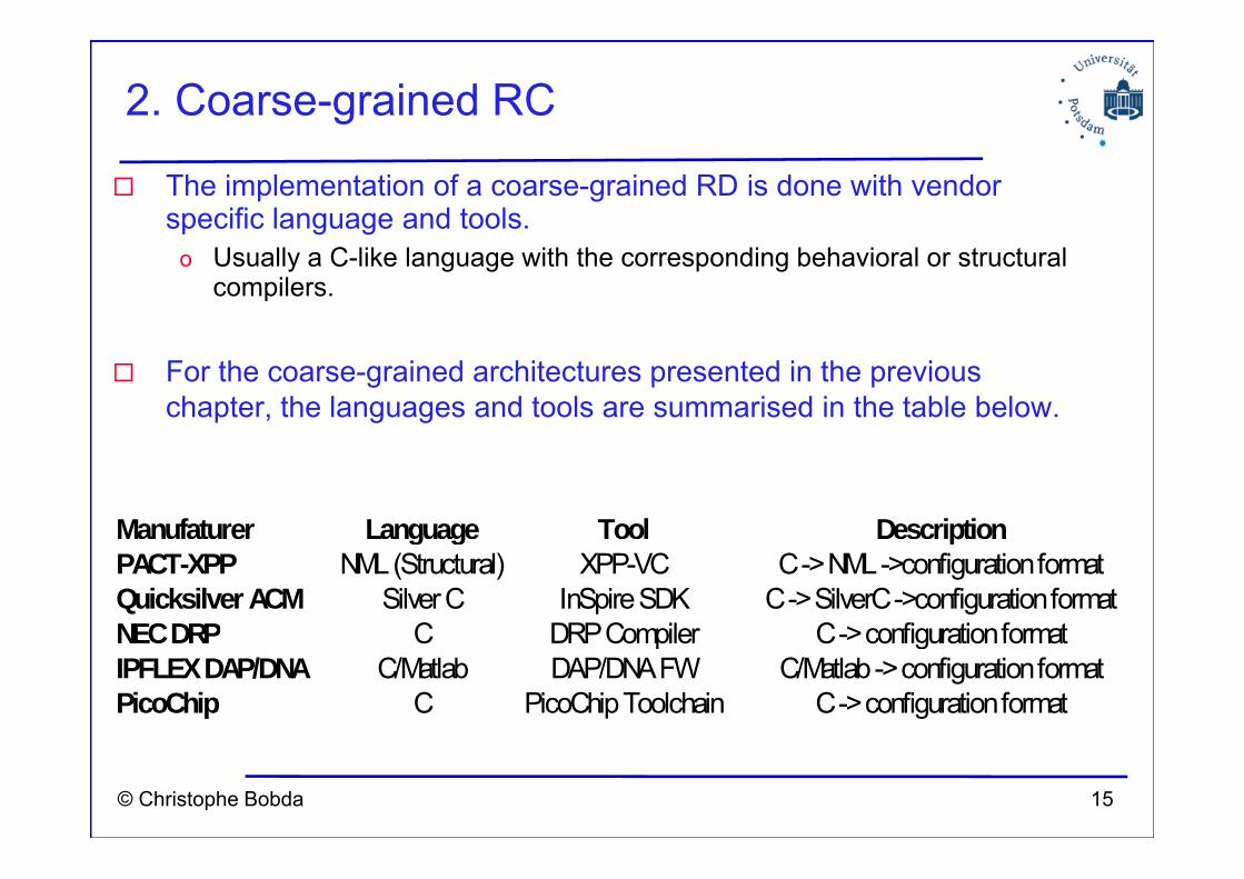
2. Coarse-grained RC
The implementation of a coarse-grained RD is done with vendor specific language and tools.
o Usually a C-like language with the corresponding behavioral or structural compilers.
For the coarse-grained architectures presented in the previous chapter, the languages and tools are summarised in the table below.
Manufaturer Language Tool Descriptiong g pPACT-XPP NML (Structural) XPP-VC C -> NML ->configuration formatQuicksilver ACM Silver C InSpire SDK C -> SilverC ->configuration formatNECDRP C DRPCompiler C->configurationformatNEC DRP C DRP Compiler C > configuration formatIPFLEX DAP/DNA C/Matlab DAP/DNA FW C/Matlab -> configuration formatPicoChip C PicoChip Toolchain C -> configuration format
15© Christophe Bobda
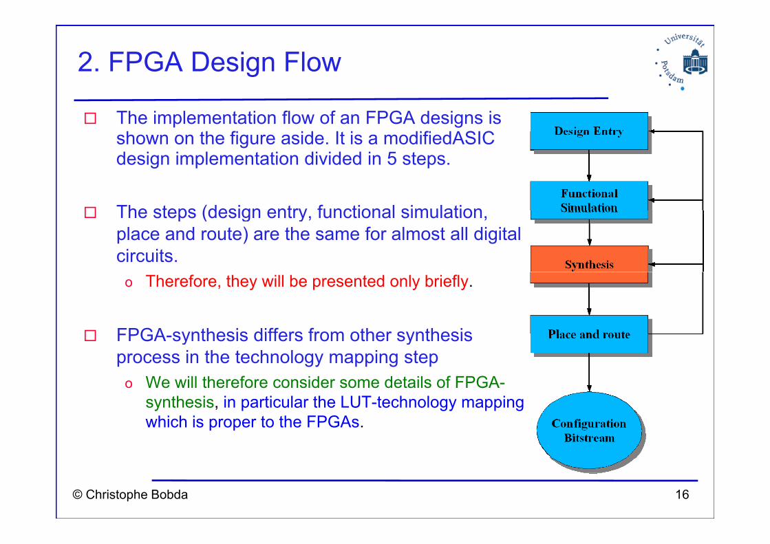
2. FPGA Design Flow
The implementation flow of an FPGA designs is shown on the figure aside. It is a modifiedASIC design implementation divided in 5 steps.
The steps (design entry functional simulationThe steps (design entry, functional simulation, place and route) are the same for almost all digital circuits.
o Therefore, they will be presented only briefly.
FPGA synthesis differs from other synthesisFPGA-synthesis differs from other synthesis process in the technology mapping step
o We will therefore consider some details of FPGA-synthesis, in particular the LUT-technology mapping which is proper to the FPGAs.
16© Christophe Bobda

2. FPGA Design Flow - Design entry
The design entry can be done witho A schematic editor:
Selection components from a (target device) and graphically connecting them together to build complex modules.
• Finite State machine (FSM) can also be entered by drawing the states and transitions either as graph or as table.
o A Hardware Description Language (HDL)• structural as well as behavioral description of complexstructural as well as behavioral description of complex
circuits.• Behavioral description: useful for designs
containing loops, Bit-vectors, ADT, FSMs.containing loops, Bit vectors, ADT, FSMs.• Structural description: emphasizes the hierarchy
in a given design.
17© Christophe Bobda

2. FPGA Design Flow – Functional Simulation
After the design entry, the functional simulation isused to logically test the functionality of the design.
o A testbench provides the design under test with inputs for which the reaction of the design is known.
The o tp ts of the circ it are obser ed on ao The outputs of the circuit are observed on a waveform and compared to the expected values.
o For simulation purpose, many operations can be used p p , y p(mod, div, etc...) in the design description.
o However only part of the code which is used for simulation can be synthesized latersimulation can be synthesized later.
o The most used HDLs are:• VHDL (behavioral, structural)VHDL (behavioral, structural)• Verilog (behavioral, structural)• Some C/C++-like languages (SystemC, HandelC,
etc )
18© Christophe Bobda
etc...)
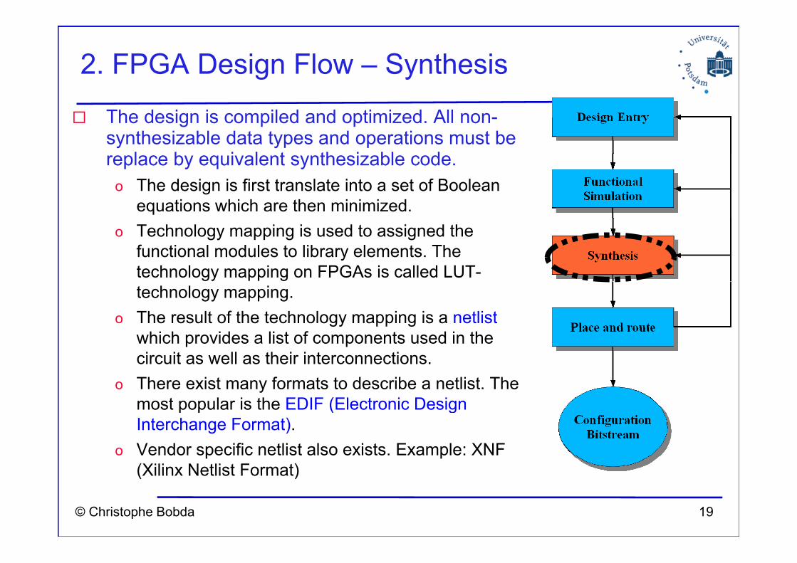
2. FPGA Design Flow – Synthesis
The design is compiled and optimized. All non-synthesizable data types and operations must be
l b i l t th i bl dreplace by equivalent synthesizable code.o The design is first translate into a set of Boolean
equations which are then minimized.o Technology mapping is used to assigned the
functional modules to library elements. The technology mapping on FPGAs is called LUT-technology mapping.
o The result of the technology mapping is a netlistwhich provides a list of components used in the p pcircuit as well as their interconnections.
o There exist many formats to describe a netlist. The most popular is the EDIF (Electronic Designmost popular is the EDIF (Electronic Design Interchange Format).
o Vendor specific netlist also exists. Example: XNF (Xilinx Netlist Format)
19© Christophe Bobda
(Xilinx Netlist Format)
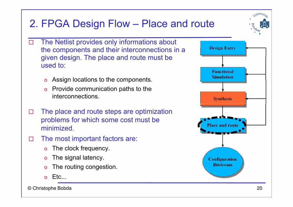
2. FPGA Design Flow – Place and routeThe Netlist provides only informations about the components and their interconnections in a given design The place and route must begiven design. The place and route must be used to:
o Assign locations to the componentso Assign locations to the components.o Provide communication paths to the
interconnections.
The place and route steps are optimization problems for which some cost must be minimizedminimized.The most important factors are:
o The clock frequency.q yo The signal latency.o The routing congestion.
20© Christophe Bobda
o Etc...
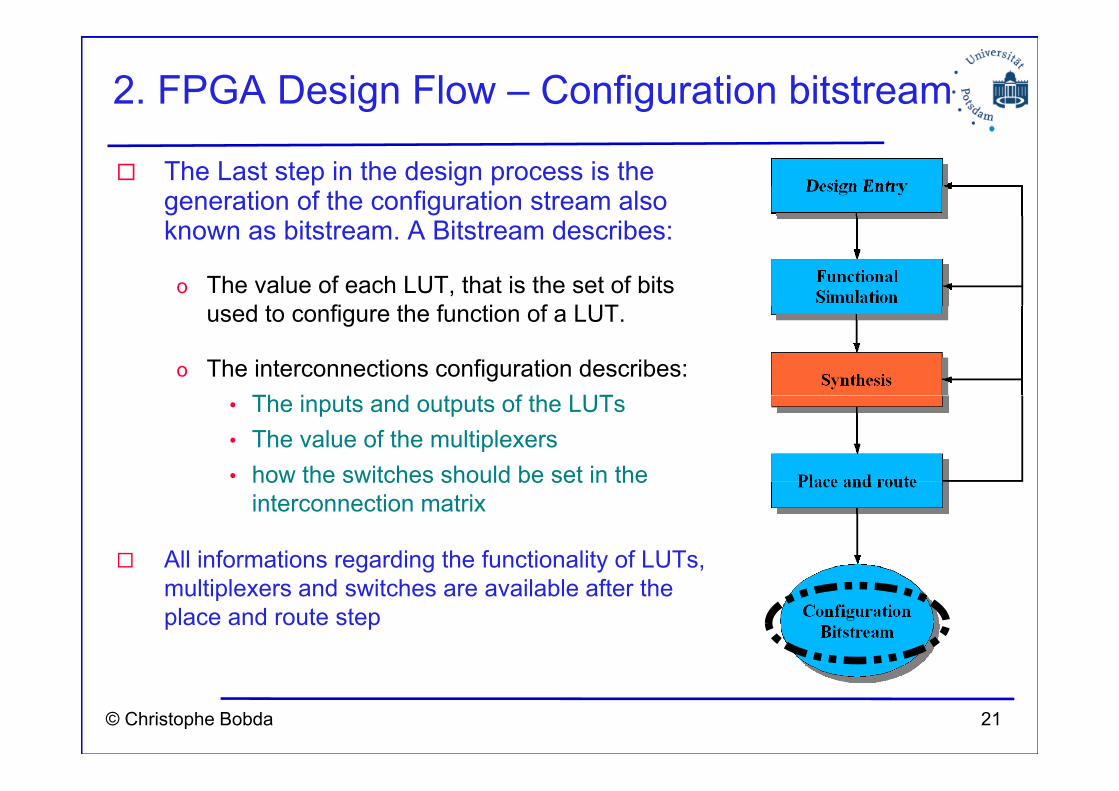
2. FPGA Design Flow – Configuration bitstream
The Last step in the design process is the generation of the configuration stream also known as bitstream. A Bitstream describes:
o The value of each LUT, that is the set of bits d t fi th f ti f LUTused to configure the function of a LUT.
o The interconnections configuration describes:Th i t d t t f th LUT• The inputs and outputs of the LUTs
• The value of the multiplexers • how the switches should be set in the
interconnection matrix
All informations regarding the functionality of LUTs, multiplexers and switches are available after the place and route step
21© Christophe Bobda

2. FPGA Design Flow – Example
Implements a Modulo 10-counter on a symetrical array FPGA with a 2x2 Logic Bl k (LB)Block (LB) .
The structure of the LBs is given in the i id I i fpicture aside. It consists of:o 2 2-inputs LUT.o 2 edge triggered T-Flipflop.o 2 edge triggered T Flipflop.
Your result should minimizeo The areao The areao The latency
22© Christophe Bobda

2. FPGA Design Flow – ExampleTruth table of the modulo 10 counter The z describe the states while the T describe the inputs of the T-FFs
Karnaugh-minimization of the functions T1, T2, T3, and T4the inputs of the T-FFs
23© Christophe Bobda
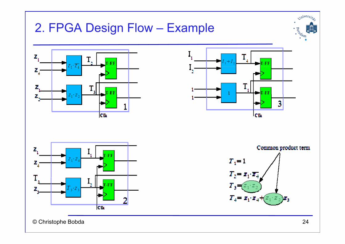
2. FPGA Design Flow – Example
24© Christophe Bobda

2. FPGA Design Flow – Example
25© Christophe Bobda