RF applications in digital signal pr ocessing - CERNcds.cern.ch/record/1100538/files/p249.pdf · RF...
35
RF applications in digital signal processing T. Schilcher Paul Scherrer Institut, Villigen, Switzerland Abstract Ever higher demands for stability, accuracy, reproducibility, and monitoring capability are being placed on Low-Level Radio Frequency (LLRF) systems of particle accelerators. Meanwhile, continuing rapid advances in digital sig- nal processing technology are being exploited to meet these demands, thus leading to development of digital LLRF systems. The first part of this course will begin by focusing on some of the important building-blocks of RF sig- nal processing including mixer theory and down-conversion, I/Q (amplitude and phase) detection, digital down-conversion (DDC) and decimation, con- cluding with a survey of I/Q modulators. The second part of the course will introduce basic concepts of feedback systems, including examples of digital cavity field and phase control, followed by radial loop architectures. Adaptive feed-forward systems used for the suppression of repetitive beam disturbances will be examined. Finally, applications and principles of system identification approaches will be summarized. 1 Introduction In this lecture we shall examine various aspects of Low-Level Radio Frequency (LLRF) systems for particle accelerators. These LLRF systems typically collect measurements of amplitude, phase, and frequency, perform various signal processing and computational processes on that data, and then use the outcome to monitor, control, and regulate RF fields in particle accelerators. The LLRF applications can be classified into monitoring, feedback, and feed-forward systems. The range of typical RF frequencies in particle accelerators varies widely starting from a few MHz (e.g., in ion accelerators) and going up to tens of GHz (e.g., high-gradient acceleration structures operating at 30 GHz). The variety of accelerators demands LLRF systems with different requirements. The boundary conditions for the LLRF systems depend on their field of application, e.g., linear or circular machines, normal or super-conducting RF systems, pulsed or CW operation, or even electron or hadron accelerators. A short incomplete list of typical LLRF applications is given in Table 1. The rapid advances in digital technology over the last decade have prepared the ground for applications of digital systems in the field of LLRF. The question arises why implementations of digital systems have found their way into LLRF applications to such a large extent. There are some disadvantages with respect to their analog counterparts but on the other hand, they offer many advantages. A comparison of digital and analog LLRF systems is given in Table 2 [1]. In feedback systems, the biggest advantage of analog systems is their short loop latency. Whenever high loop bandwidths are required, analog systems still continue to be the only realistic alternative. Table 1: Typical low-level RF applications Application Task Cavity field loops Control amplitude and phase of accelerating RF fields in cavities Tuner loops Control resonant frequencies of RF cavities Radial and phase loops Control radial beam positions and phases in circular machines Klystron loops Control amplitude and phase of klystrons RF gymnastics Control bunch splitting and merging in circular machines 249
Transcript of RF applications in digital signal pr ocessing - CERNcds.cern.ch/record/1100538/files/p249.pdf · RF...

RF applications in digital signal processing
T. SchilcherPaul Scherrer Institut, Villigen, Switzerland
AbstractEver higher demands for stability, accuracy, reproducibility, and monitoringcapability are being placed on Low-Level Radio Frequency (LLRF) systemsof particle accelerators. Meanwhile, continuing rapid advances in digital sig-nal processing technology are being exploited to meet these demands, thusleading to development of digital LLRF systems. The first part of this coursewill begin by focusing on some of the important building-blocks of RF sig-nal processing including mixer theory and down-conversion, I/Q (amplitudeand phase) detection, digital down-conversion (DDC) and decimation, con-cluding with a survey of I/Q modulators. The second part of the course willintroduce basic concepts of feedback systems, including examples of digitalcavity field and phase control, followed by radial loop architectures. Adaptivefeed-forward systems used for the suppression of repetitive beam disturbanceswill be examined. Finally, applications and principles of system identificationapproaches will be summarized.
1 IntroductionIn this lecture we shall examine various aspects of Low-Level Radio Frequency (LLRF) systems forparticle accelerators. These LLRF systems typically collect measurements of amplitude, phase, andfrequency, perform various signal processing and computational processes on that data, and then use theoutcome to monitor, control, and regulate RF fields in particle accelerators. The LLRF applications canbe classified into monitoring, feedback, and feed-forward systems. The range of typical RF frequenciesin particle accelerators varies widely starting from a few MHz (e.g., in ion accelerators) and going up totens of GHz (e.g., high-gradient acceleration structures operating at 30 GHz). The variety of acceleratorsdemands LLRF systems with different requirements. The boundary conditions for the LLRF systemsdepend on their field of application, e.g., linear or circular machines, normal or super-conducting RFsystems, pulsed or CW operation, or even electron or hadron accelerators. A short incomplete list oftypical LLRF applications is given in Table 1. The rapid advances in digital technology over the lastdecade have prepared the ground for applications of digital systems in the field of LLRF. The questionarises why implementations of digital systems have found their way into LLRF applications to such alarge extent. There are some disadvantages with respect to their analog counterparts but on the otherhand, they offer many advantages. A comparison of digital and analog LLRF systems is given in Table 2[1]. In feedback systems, the biggest advantage of analog systems is their short loop latency. Wheneverhigh loop bandwidths are required, analog systems still continue to be the only realistic alternative.
Table 1: Typical low-level RF applications
Application TaskCavity field loops Control amplitude and phase of accelerating RF fields in cavitiesTuner loops Control resonant frequencies of RF cavitiesRadial and phase loops Control radial beam positions and phases in circular machinesKlystron loops Control amplitude and phase of klystronsRF gymnastics Control bunch splitting and merging in circular machines
249

Table 2: Comparison of digital versus analog RF applications
Digital Analogimplementation learning curve + software effort easier / knownlatency longer shortdata acquisition/control (I/Q) sampling (also direct) amplitude/phase,
or Digital Down Conversion (DDC) IF down conversionalgorithms sophisticated simple
state machines, exception handling linear, time-invariant(example: PID control)
multi-user full limitedremote control + diagnostics easy, often no additional difficult,
hardware necessary often extra HW necessaryflexibility/reconfigurability high, easy upgrades limiteddrift/tolerance no drifts, repeatability drift (temperature, etc.),
component tolerancesignal transport distance longer shortwithout distortionsradiation sensitivity high small
However, the increasing processing speed of digital systems now often allows them to cover the loopbandwidth demands and therefore supersede analog systems.
To characterize digital LLRF systems, we can break them down into four main building blockswhich are shown in Fig. 1. RF signals from the accelerator, e.g., from probe antennas or directionalcouplers, are down-converted (if necessary) and conditioned in the first block, which typically includesfiltering, amplification and/or attenuation. The second block comprises the digitization process, while
Fig. 1: Main blocks of RF applications. Feedback and feed-forward systems close the loop (blue box) whilemonitoring applications provide the processed RF field information to other sub-systems or to the control system.
the third block deals with the digital signal processing of the sampled RF fields. Depending on the hard-ware and algorithms, the extracted information is supplied to the control system for monitoring purposesor to any other sub-system requiring this information. In case of feedback applications, which close thesignal path, the correction signals resulting from the control algorithms usually need to be converted backto analog RF signals of precise amplitudes, phases, and frequencies. This can be achieved by digital-to-analog converters and various up-conversion schemes—very often so-called vector modulators areused. Basic principles of these techniques will be described in the section covering the fourth buildingblock. These four basic building blocks which form LLRF systems also form the basis of many otheraccelerator applications, e.g., diagnostic applications like beam-position monitoring measurements, or-
T. SCHILCHER
250

bit feedbacks, and bunch-by-bunch feedback systems. Sharing of digital hardware platforms providesgrounds for common development. As in every feedback system, the ultimate remaining error is dom-inated by the measurement process which includes systematic errors, accuracy, linearity, repeatability,stability, resolution, and noise. In the following sections, we shall first discuss these four building blocksbefore proceeding on to an introduction to feedback systems, adaptive feed-forward algorithms, andsystem identification.
2 Signal conditioning and down conversionDigital systems require the transformation of analog signals into the digital domain. This is achievedby analog-to-digital converters (ADC, A/D converters). In most cases, analog preprocessing has to beapplied prior to the A/D conversion because the sampling frequencies, analog input bandwidths, and thebit resolution of ADCs are limited. This preprocessing typically consists of amplitude scaling (ampli-fication, attenuation) along with filtering and frequency translation to an intermediate frequency or tobaseband. The digitization of high-frequency carrier signals is very often not possible or reasonable. Al-though today’s ADCs already reach the giga-samples per second domain with even higher analog inputbandwidths, the requirements for ADC clock and aperture jitter become more and more stringent. Thisis even more critical with under-sampling schemes in which signals are sampled outside the first Nyquistzone, which means any clock and/or aperture jitter has a large impact on the resulting error. The systemdesigner always has to evaluate the trade-off between sampling speed and dynamic range of an ADC.Each additional effective bit of an ADC provides 6 dB more in terms of dynamic range. Very often itis better to use analog circuits in conjunction with ADCs to implement automated gain control (AGC)functions to ensure that the signal to be sampled falls within the ideal dynamic range of the chosen ADC.Taking into account these technical limits, frequency translations to lower intermediate frequencies areessential in many RF applications. This is usually achieved by RF mixers, whose basic functionality willpresently be introduced. Since frequency conversions are non-linear operations, RF mixers cannot be re-alized by linear-time-invariant (LTI) components or circuits. Instead, the translation is achieved by eithertime varying or non-linear circuits, e.g., diodes. An ideal mixer is usually represented by a multipliersymbol (see Fig. 2) with two input ports and one output port. The signal at the output port is the vector
Fig. 2: Ideal RF mixer with input signals yRF (t) and yLO(t)
multiplication of the signals at the two input ports. One of the input signals is the reference signal, thelocal oscillator (LO). Using some trigonometric product-to-sum identities and assuming two sinusoidalinput signals with amplitudes ARF , ALO and frequencies fRF , fLO, the multiplied output signal yIFcan be represented as
yIF (t) = yRF (t) · yLO(t)
=12ALOARF ·
(sin[(ωRF − ωLO) t+ (ϕRF − ϕLO)
]︸ ︷︷ ︸lower sideband
+ sin[(ωRF + ωLO) t+ (ϕRF + ϕLO)
]︸ ︷︷ ︸upper sideband
). (1)
RF APPLICATIONS IN DIGITAL SIGNAL PROCESSING
251

The input signal is translated to two output frequencies, the upper (fRF +fLO) and the lower (fRF−fLO)sideband signals. Mixers are used for down- and up-conversion. In the case of down-conversion, the RFand LO signals are high-frequency inputs while the resulting output signal is the intermediate frequencysignal [Fig. 3(a)]. Likewise, an intermediate frequency can be used as input to perform an up-conversion[Fig. 3(b)]. Usually, either the upper or the lower sideband of the mixing process is selected by filtering
Fig. 3: (a) down conversion and (b) up conversion schemes with RF mixers
the output signal. Note that for a given LO frequency, signals at frequencies LO±IF are converted tothe same IF frequency. Therefore care has to be taken by applying proper filtering in order to avoid theconversion of any noise or signal at the image frequency to the IF frequency [Fig. 3(a)], otherwise it candegrade system performance, often severely. For receiver applications, to which particular attention willnow be given, the lower sideband is extracted by low-pass filtering. With Eq. (1) this yields for the IFsignal
yIF (t) = AIF · sin(ωIF t+ ϕIF
)with the frequency, amplitude and phase definition
ωIF = ωRF − ωLO,AIF = 1
2ALOARF ∼ ARF with constant ALO ,
ϕIF = ϕRF − ϕLO ∼ ϕRF with constant ϕLO .
With a constant LO signal, i.e., with a constant ALO and ϕLO, the amplitude and phase of the down-converted signal are directly proportional to those of the input signal, in other words, all of the basicproperties of an RF signal are conserved in the frequency conversion process. In this context, two im-portant facts should be highlighted: first of all, a phase change or phase jitter at fRF is exactly the samephase change at the IF frequency fIF . As an example, a 1◦ phase change at 3 GHz corresponds also toa 1◦ phase change at any arbitrary IF frequency. Secondly, timing jitter of a given magnitude at a higherfrequency leads to a bigger phase variation than at a lower frequency. This has to be taken into account
T. SCHILCHER
252

when deciding whether an RF signal should be directly sampled or down-converted first. ADC clockjitters are therefore much more critical in direct sampling applications and tougher requirements have tobe applied. As an illustration, a 10 ps clock jitter at 500 MHz corresponds to 1.8◦ phase variation whilethe same clock jitter results in only 0.18◦ phase variation at 50 MHz.
So far, ideal mixers have been considered. As pointed out earlier, real mixers are non-lineardevices. In addition to the desired ideal mixing product, their output spectra contain many undesiredspurious signals which are located at mfRF ± nfLO. Figure 4 depicts the output spectrum of a down-conversion mixer. The image frequency is denoted by IM . Usually, the signal at the mixer output is
Fig. 4: Output spectrum of a real mixer
filtered by a low-pass filter in order to suppress the undesired spurs sufficiently. Introducing low-passfilters with a steep roll-off, however, will mean a trade-off between good suppression and increased groupdelay which is very important for low latency and feedback applications. Other common ways to reducespurious outputs are the use of double-balanced mixers and image rejection mixers to minimize imagemixing.
3 Detection of amplitude and phase in digital systemsSeveral techniques can be applied to detect amplitude and phase of RF signals in digital systems, anoverview of which is shown in Fig. 5. Common amplitude detectors like Schottky diodes and phasedetectors [2] provide amplitude and phase information as a continuous analog signal which can be dig-itized by ADCs for further processing [Fig. 5(a)]. In contrast to this, the polar representation of an RFsignal can also be decomposed into its Cartesian representation (I/Q, see Section 3.1) by analog IQdemodulators. The individual I/Q components can then be digitized [Fig. 5(b)]. A third alternativeis the so-called digital IQ sampling and Digital Down Conversion (DDC) where an RF signal is firstdown-converted to an intermediate frequency and then directly digitized. Depending on the frequency,the down-conversion process can be omitted. The I/Q information is extracted from these samples ina purely digital way. These techniques will be further discussed in Section 3.1. Since the focus of thislecture is on digital signal processing, the first two detection schemes will not be dealt with any further.
3.1 IQ samplingThe terminology ‘IQ’ originates from the representation of an RF signal which can be in either polar(amplitude/phase representation) or in Cartesian coordinates. Any sinusoidal RF signal
y(t) = A · sin(ωt+ ϕ0) (2)
can be modelled as a phasor which is a rotating vector with amplitudeA, frequency ω, and an initial phaseϕ0. A positive frequency corresponds to an anticlockwise rotating phasor, which can be decomposed into
RF APPLICATIONS IN DIGITAL SIGNAL PROCESSING
253

Fig. 5: different schemes of amplitude and phase detection in digital systems
its sin and cos components using basic trigonometric functions.
y(t) = A cosϕ0︸ ︷︷ ︸=:I
sinωt+A sinϕ0︸ ︷︷ ︸=:Q
cosωt
y(t) = I · sinωt+Q · cosωt . (3)
The amplitude of the sine component can be defined as the in-phase component (I), while the amplitudeof the cosine component is called the quadrature-phase component (Q). This definition is somewhatarbitrary and can therefore be found inversed in the literature. The Cartesian representation of an RF sig-nal (I/Q) is widely used in numerical applications. The well-known relationship between Cartesian andpolar coordinates [Eq. (4)] makes switching between both representations possible—if necessary, and ifcomputing resources allow the time-consuming calculation of square roots and trigonometric functions.Sampling of a sinusoidal RF signal with an ADC delivers only one component of the rotating phasor
Fig. 6: Phasor representation of RF signal
I = A · cosϕ0 A =√I2 +Q2
Q = A · sinϕ0 ϕ0 = atan(QI
) (4)
at a time. Nevertheless it is both easy and possible to extract I/Q information based on the sampleddata stream, as will now be shown. We assume that the vertical component is measured by the ADC(this assumption is also arbitrary but it has no consequence on the following results). The goal of sam-pling the RF or IF signal is to extract its amplitude/phase or I/Q information, respectively. If I/Q ofthe rotating phasor is known initially and measured again later at a well-defined time, an algorithm canrotate the phasor back to an initial reference phasor. A comparison of these two measurements will thenreveal whether the incoming RF signal has changed its amplitude and phase. The usual IQ sampling is
T. SCHILCHER
254

achieved if the sampling frequency fs and the intermediate frequency fIF (or in general, the incomingRF signal) are related by
fs = 4 · fIF . (5)
In this case, the phase advance between two samples amounts to 90◦. With Eq. (3) the digitization atfour consecutive sampling times results in
ωt0 = 0 : y(t0) = Qωt1 = π/2 : y(t1) = Iωt2 = π : y(t2) = −Qωt3 = 3π/2 : y(t3) = −I .
(6)
This is illustrated in Fig. 7. At each sampling time, the I and Q components of the phasor can bedetermined by two consecutive samples, y(ti) and y(ti+1). These vectors have to be rotated backwards
Fig. 7: IQ sampling with 90◦ phase advance between consecutive samples
by ∆ϕi = 0◦, –90◦, –180◦ and –270◦ in order to compare them with the initial vector. The underlyingrotation algorithm is (
IQ
)ti
=(
cos ∆ϕi − sin ∆ϕisin ∆ϕi cos ∆ϕi
)·(yi+1
yi
). (7)
The rotation algorithm is carried out at the sample rate fs. It is based on the assumption that the in-coming RF signal does not change its amplitude and phase substantially between two samples since thecomponents of the (I/Q) phasor are based on two successive samples. If we were to choose to measurethe horizontal component of the phasor with an ADC, the result would be exactly the same, which caneasily be seen in Fig. 7. Instead of the sequence Q, I , –Q, –I we would measure the sequence I , –Q, –I ,Q which only corresponds to a phase shift of 90◦.
The restriction to choose a sampling frequency four times the carrier frequency simplifies thecalculation since the elements of the rotation matrix only consist of 1, 0 and –1. Despite this fact, it ispossible in principle to choose the sampling frequency such that it is a multiple of the IF frequency.
fs/fIF = m, m : integer .
In this case, the phase difference between two samples amounts to
∆ϕ =2πm
. (8)
As long as the input signal does not change substantially, each IF period is sampled at the same locationon the circle in the IQ plane. With two consecutive samples (yn = Qn, yn+1 = Qn+1) and the rotationof the I/Q vector at time tn+1 to the vector at time tn by the angle −∆ϕ, a set of linear equations isobtained. (
InQn
)=(
cos ∆ϕ sin ∆ϕ− sin ∆ϕ cos ∆ϕ
)·(In+1
Qn+1
).
RF APPLICATIONS IN DIGITAL SIGNAL PROCESSING
255

Solving this set of equations to eliminate In+1, Qn+1 yields(InQn
)=
1sin ∆ϕ
·(
1 − cos ∆ϕ0 sin ∆ϕ
)·(yn+1
yn
).
Similar to the case where the IF frequency is sampled four times per period, the phasor (In, Qn) has tobe rotated backwards to the initial phasor (I0, Q0) by a rotation angle −n∆ϕ where the phase advance∆ϕ is defined in Eq. (8).(
I0
Q0
)=
1sin ∆ϕ
·(
cosn∆ϕ − cos(n+ 1)∆ϕ− sinn∆ϕ sin(n+ 1)∆ϕ
)·(yn+1
yn
).
In the most general case, the initial phasor can also be rotated by a user defined angle −ϕ in order tomatch initial conditions. Including this last rotation the (I ,Q) vector can be obtained by(
IQ
)=
1sin ∆ϕ
·(
cos (ϕ+ n∆ϕ) − cos (ϕ+ (n+ 1)∆ϕ)− sin (ϕ+ n∆ϕ) sin (ϕ+ (n+ 1)∆ϕ)
)·(yn+1
yn
). (9)
The calculation of I and Q belongs to the class of FIR filters of first order since the values are basedon two consecutive samples. This sequence of processing is illustrated in Fig. 8. Although the phase
Fig. 8: IQ sampling with a phase advance of ∆ϕ = 2π/m between consecutive samples
advance can be chosen as illustrated in Eq. (8), the calculation of I and Q becomes extremely sensitiveto noise and sampling errors if the phase advance is far away from 90◦ or 270◦ [see Eq. (9)].
There are a number of potential problems associated with this typical mode of IQ sampling(∆ϕ = 90◦). DC offsets at the input of the ADC or phase advances between samples (which differfrom the expected 90◦) systematically result in a ripple with frequency fIF . These errors are easily de-tectable since their signatures reveal their origin. Other error sources are much more difficult to identifyat first glance. Non-linearities of mixers and differential non-linearities of ADCs generate higher har-monics of the input signal frequency fIF . Sampling this signal four times per period maps the secondharmonic on the Nyquist frequency, while the third harmonic aliases directly on the IF frequency again.In general, all odd harmonics alias to the carrier frequency while even harmonics alias to DC or to theNyquist frequency, respectively (see Fig. 9). Any harmonics which map onto the IF frequency are in-distinguishable from the carrier by standard IQ sampling. As the carrier frequency and phase changes,the distortion changes, resulting in false measurement data.
3.2 Non-IQ samplingA solution to the problems described is to change the sampling frequency in such a way that the followingrelation holds:
fs =N
M· fIF ⇐⇒ N · Ts = M · TIF with M,N : integer .
T. SCHILCHER
256

Fig. 9: Spectrum of IQ sampling with a phase advance of 90◦ between consecutive samples
The above is equivalent to taking N samples in M successive IF periods. Depending on the valueschosen for M,N the circle in the IQ plane is now sampled at different locations where the samples onlyrepeat after M IF periods. The phase advance between two consecutive ADC readings is
∆ϕ = ωIFTs = 2πTsTIF
= 2πM
N.
Expressing the N successive samples with Eq. (3), the result is a set of linear equations [3], [4].
y0 = I · sinϕ0 + Q · cosϕ0
y1 = I · sinϕ1 + Q · cosϕ1
y2 = I · sinϕ2 + Q · cosϕ2 with ϕi = i ·∆ϕ = i · 2πMN , i: integer ....y(N−1) = I · sinϕ(N−1)+ Q · cosϕ(N−1)
(10)
In the ideal case of no measurement errors, any two equations of this set would give a solution common toboth for I,Q. Under real conditions with noise, quantization errors, and clock jitter, the over-constrainedsystem of equations can be solved by applying the Least Mean Square algorithm (LMS). The basis forthis algorithm is to minimize the function
f(I,Q) =N−1∑i=0
(I · sinϕi +Q · cosϕi − yi)2 . (11)
The conditions for a minimum are vanishing derivatives with respect to I and Q.
∂f
∂I= 0,
∂f
∂Q= 0 .
This yields
∂f
∂I= 2I
N−1∑i=0
sin2 ϕi + 2QN−1∑i=0
sinϕi cosϕi − 2N−1∑i=0
yi sinϕi = 0
∂f
∂Q= 2Q
N−1∑i=0
cos2 ϕi + 2IN−1∑i=0
sinϕi cosϕi − 2N−1∑i=0
yi cosϕi = 0 . (12)
With the definitions
p11 =N−1∑i=0
sin2 ϕi, p12 = p21 =N−1∑i=0
sinϕi cosϕi, p22 =N−1∑i=0
cos2 ϕi
RF APPLICATIONS IN DIGITAL SIGNAL PROCESSING
257
s1 =N−1∑i=0
yi sinϕi, s2 =N−1∑i=0
yi cosϕi ,
Eq. (12) can be written asp11 · I + p12 ·Q = s1
p21 · I + p22 ·Q = s2 .
The coefficients p12 and p21 can be simplified using the definition for ϕi of Eq. (10).
p12 = p21 =12
N−1∑i=0
sin 2ϕi =12
N−1∑i=0
sin 4πMi
N︸ ︷︷ ︸=0
= 0 .
Likewise, the coefficients p11 and p22 can be calculated to
p11 =12
N−1∑i=0
(1− cos 2ϕi) =N
2, p22 =
12
N−1∑i=0
(1 + cos 2ϕi) =N
2.
Therefore the I and Q values can be simply calculated by
I =2N·N−1∑i=0
yi · sin(i ·∆ϕ) (13)
Q =2N·N−1∑i=0
yi · cos(i ·∆ϕ) . (14)
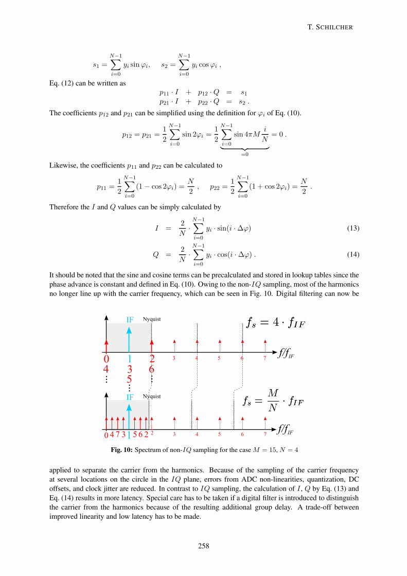
It should be noted that the sine and cosine terms can be precalculated and stored in lookup tables since thephase advance is constant and defined in Eq. (10). Owing to the non-IQ sampling, most of the harmonicsno longer line up with the carrier frequency, which can be seen in Fig. 10. Digital filtering can now be
Fig. 10: Spectrum of non-IQ sampling for the case M = 15, N = 4
applied to separate the carrier from the harmonics. Because of the sampling of the carrier frequencyat several locations on the circle in the IQ plane, errors from ADC non-linearities, quantization, DCoffsets, and clock jitter are reduced. In contrast to IQ sampling, the calculation of I , Q by Eq. (13) andEq. (14) results in more latency. Special care has to be taken if a digital filter is introduced to distinguishthe carrier from the harmonics because of the resulting additional group delay. A trade-off betweenimproved linearity and low latency has to be made.
T. SCHILCHER
258

3.3 Digital Down Conversion—DDCAnother possible way of extracting amplitude and phase information from a sampled carrier signal is bymeans of Digital Down Conversion (DDC), sometimes also referred to as Digital Drop Receiver (DDR).In many RF applications, the band of interest of an RF signal lies around a carrier or IF frequency. Thefrequency band of interest is very often narrow compared to the carrier frequency itself. According tothe Nyquist theorem, the sampling rate of a band-limited signal must be at least twice the highest analogfrequency component in order to be able to reconstruct the signal fully. This leads to high data rates andimposes high demands on subsequent digital processing stages. However, Nyquist–Shannon’s theoremstates that the sampling frequency only has to be at least twice the maximum information bandwidth.Digital down conversion is a technique which takes a band-limited high-sample-rate digitized signal,shifts the band of interest to a lower frequency and reduces the sample rate while retaining all the in-formation. The basic function of DDC is shown in Fig. 11. To illustrate the DDC principle, we assume
Fig. 11: Basic principle of Digital Down Conversion (DDC)
a 40 MHz carrier (IF signal). A band-limited signal with a bandwidth of 1 MHz is located around thecarrier frequency. If oversampling is applied, sampling has to be carried out with a frequency of at least82 MHz. However, an output sample rate of just 2 MHz would be sufficient to meet the requirement ofShannon’s theorem if the band of interest is first shifted to baseband.
Although DDC can be implemented on Digital Signal Processors (DSPs), the main applicationarea is on Application Specific Integrated Circuits (ASICs) or Field Programmable Gate Arrays (FPGAs).DDC can be divided into two classes, wideband and narrowband, based on their decimation ratio. Thesampling rate of wideband signals is typically reduced by a smaller amount (decimation ratio < 32). Thiscan be achieved by FIR or so-called multi-rate FIR filters. Narrowband DDC provides large decimationratios of more than 32, consequently their implementation on FPGA with FIR filters would take toomany gates. A better approach is the use of Cascaded Integrator Comb (CIC) filters (see later in thislecture). A digital down converter is composed of three major building blocks (see Fig. 12) which willbe addressed in the following sub-sections. The digital mixers convert the incoming digitized RF signal
DDC building blocks:
– mixer (digital mixer)– local oscillator
(numerically controlled oscillator,NCO)
– decimating low-pass filter (LPF)Fig. 12: Main building blocks of Digital Down Conversion
down to baseband and are realized as ideal multipliers, just like their ideal analog counterpart. Thelocal oscillator inputs are supplied by numerically controlled oscillators (NCOs). As shown in Section 2,the resulting output consists of the sum and the difference frequency with respect to the input frequency.The purpose of the subsequent low-pass filter is to suppress the sum frequency component and to provide
RF APPLICATIONS IN DIGITAL SIGNAL PROCESSING
259

anti-aliasing filtering. This is necessary in order to limit the signal spectrum prior to decimation. Thedecimating anti-aliasing filter is often implemented as CIC filter and/or FIR filter.
3.3.1 Numerically Controlled Oscillator—NCOThe numerically controlled oscillator in a DDC is implemented as a quadrature digital oscillator whichgenerates a stream of sine and cosine samples. If the frequency of the NCO is chosen to match the carrierfrequency, the difference signals at the outputs of the digital mixers represent the I and Q componentsof the input signal. One of the advantages of the NCO is that the two sine and cosine output signalsare perfectly synchronized, since they are derived from a common clock. Moreover, the signals havea very precise 90◦ phase shift. There are several ways to implement a NCO. Its basic functionality isthat of a phase accumulator and a phase-to-amplitude conversion block (see Fig. 13). A programmable
Fig. 13: Basic principle of a Numerically Controlled Oscillator (NCO)
phase increment is added within the phase accumulator at each clock cycle. This phase increment isdetermined by the tuning word M . The resulting total phase is then converted to the correspondingamplitude value taken from a memory-based lookup table in which a sine wave is stored. A phase roll-over is achieved easily if the table size is chosen to be a binary multiple. In this case, the roll-over takesplace automatically. Numerically controlled oscillators have several advantages compared to their analogcounterparts. First of all, the tuning word is programmable, which means that almost every frequency upto nearly half the clock frequency (Nyquist frequency) can be chosen by means of the software. NCOshave extremely fast hopping speeds in tuning the output frequency, which means they are extremelyfrequency agile. The frequency change occurs immediately after loading a new phase increment intothe tuning word M . In addition, this technique provides a phase-continuous frequency hop withoutover- or undershoot and without the loop settling time anomalies encountered in analog circuit variableoscillators. The sine lookup table can contain a full sine wave or just one quarter of one; this is sufficientfor reconstruction of the sine wave and reduces the amount of memory space required (however, theadditional calculations necessary to end up with the correct amplitude have to be traded off against thesaving of the memory space). The total size of the memory is dependent on the desired resolution (outputamplitude bit-width) of the entries and on the number of entries stored in the table. The achievable outputfrequency fout is a function of the clock frequency fCLK , the tuning word M , the bit width of the phaseaccumulator N , and is given by
fout = M · fCLK2N
.
NCOs can reach very high frequency resolutions if the word length of the phase accumulator is chosenproperly. As an example, if a clock frequency of 50 MHz is assumed and the phase accumulator widthis set to 32-bits, the resulting frequency tuning resolution will be ∆f= 12 mHz. On the other hand, thequestion that needs to be addressed is whether the same number of entries in the lookup table is neededas phase outputs are possible. Sticking to our example of 32-bit phase accumulation, and assuming anamplitude bit width of 8-bits, we would require a 4 GByte lookup table. One way out of such an imprac-tical implementation is the method of phase truncation. Before the resulting phase of the accumulator islooked up in the table, it is truncated to a defined number of upper bits while the phase in the accumulatoris preserved. This reduces the need for large memories tremendously. However, one consequence of thisapproach is the introduction of errors in the phase-to-amplitude conversion process. Regardless of the
T. SCHILCHER
260

chosen tuning word, these truncation errors are periodic and appear as line spectra in the frequency do-main (although certain tuning words result in no phase truncation errors at all, which should be obvious).These lines in the spectra are known as phase truncation spurs which reduce the Spurious Free DynamicRange (SFDR) of the output spectrum.
Although NCOs for digital down conversion do not require more elements than are shown in theblock diagram shown in Fig. 13, we shall briefly extend this chapter to Direct Digital Synthesis for thesake of completeness. Direct Digital Synthesis or DDS is based on the same building blocks as usedfor NCO but is extended by a DAC to generate freely programmable, high-frequency, analog waveforms(see Fig. 14). The staircase-like output of the DAC (zero-order-hold function) implies that the output
Fig. 14: basic principle of Direct Digital Synthesis (DDS) Fig. 15: inverse sin(x)/x correction at the out-put of DDS
amplitude spectrum follows a sin(x)/x function. This roll-off can be quite significant if higher outputfrequencies are desired. A solution to this problem is to pre-compensate the roll-off by digital inversesin(x)/x filters (also called inverse sinc filters) before the data is sent to the DAC (Fig. 15). In thisway, flat output amplitudes within ±0.1 dB over a bandwidth of 80% of the Nyquist frequency can beobtained. In modern DDS chips, the sin(x)/x correction is already built in.
3.3.2 Cascaded Integrator Comb filter—CICAs the final blocks in the DDC application, Cascaded Integrator Comb (CIC) filters are well suited asdecimating low-pass filters. They belong to the class of multi-rate FIR filter which performs decimationor interpolation. This type of filter was introduced by Eugene Hogenauer in 1981 [5]. A CIC filter is acomputationally efficient implementation of a narrowband low-pass filter; they require no multiplication,as we shall now see. The two basic building blocks of a CIC filter are an integrator and a comb (seeFig. 16). The integrator is a one-pole IIR filter with a unity feedback coefficient. The difference equation
basic integrator
y[n] = y[n− 1] + x[n]
transfer function:HI(z) =
11− z−1
basic comb
y[n] = x[n]− x[n−D]
transfer function:HC(z) = 1− z−D (15)
Fig. 16: Basic elements of a CIC filter
of the integrator and the corresponding transfer function are given in Fig. 16. As usual in digital signal
RF APPLICATIONS IN DIGITAL SIGNAL PROCESSING
261

processing theory, the delay by one clock operator (z−1) in the z-domain has been introduced. In a combfilter, a delayed version of the input is subtracted from itself, which causes constructive and destructiveinterference at the output. The resulting frequency response consists of a series of equally spaced spikes,which resemble a comb. The difference equation of the comb filter and its transfer function are alsogiven in Fig. 16. The parameter D is often referred to as differential delay. In general, a cascade ofM integrators and the same number of comb filters make up an M stage CIC filter. Additionally, arate changer is inserted between integrator and comb, which changes the data rate by a factor of R [seeFig. 17(a)]. The decimation operation ↓R means to discard all but every R th sample. The integrators
a) decimating CIC filter
b) interpolating CIC filterFig. 17: Basic structure of a decimating (a) and interpolating (b) CIC filter
push date at a rate fin while the comb filter stages operate at a reduced rate fout = fin/R, whichminimizes power consumption in the high-speed digital hardware. Likewise, an interpolating CIC filteris composed of the same building blocks as a decimating CIC filter, only the sequence of integrators andcombs are exchanged and a rate expander is inserted in between [Fig. 17(b)]. Thus this structure of CICfilters clearly reveals that only additions and subtractions are required for their implementation. The totaltransfer function of the decimating CIC filter is obtained by multiplying the individual transfer functionsof the building blocks. However, care has to be taken with the comb transfer function since the combstages subsequently operate at a reduced clock rate. If we refer the comb transfer function to the highinput rate fin, we have to replace the differential delay D in Eq. (15) by R ·D, since a delay of D at thereduced clock rate fout corresponds to R · D clock cycles with respect to fin. The transfer function ofthe basic comb filter after the rate changer is then given by
HC(z) = 1− z−RD .
The total transfer function of an M stage CIC filter is therefore expressed by
H(z) = (HI)M (HC)M =(1− z−RD)M
(1− z−1)M=
(RD−1∑k=0
z−k)M
, (16)
where the geometric sum is used to express H(z) as a cascade of M FIR filters. Although initially itmay have seemed that a CIC filter could be unstable—since it contains poles from the integrator—it isalways stable because it is a pure FIR filter.
T. SCHILCHER
262

Up to now, the building blocks of CIC filters have been introduced without regard to any otherparticular motivation. An alternative approach to understanding the structure of CIC filters can be foundby looking at recursive running-sum filters, which are well-known. In fact, CIC filters are derived fromthe concept of those filters [6]. In the following, we shall begin with a moving average filter (or box-carfilter) of length N and demonstrate how this structure very closely resembles a CIC filter of first order.The difference equation of a moving average filter is given by
y[n] =1N
(x[n] + x[n− 1] + · · ·+ x[n−N + 1]
)=
n∑k=n−N+1
( 1N· x[k]
). (17)
This is a standard FIR filter with equal coefficients. The corresponding transfer function can be easilydeduced from this equation and can be expressed as
H(z) =1N
(1 + z−1 + · · · + z−(N−1)
)=
1N
N−1∑k=0
z−k =1N
1− z−N1− z−1
. (18)
Here the formula for a geometric series has been used to represent the sum in a more convenient way.An alternative implementation of this box-car filter is the recursive running-sum. Instead of summing upall past N elements, it is sufficient to add only the latest scaled new sample x[n] to the previous averagevalue y[n− 1] and to subtract the oldest scaled sample x[n−N ].
recursive running-sum: y[n] = y[n− 1] +1N
(x[n]− x[n−N ]
)The recursive running-sum can also be calculated in a slightly different, cascaded way. RewritingEq. (17) to
y[n] =1N
( n∑k=−∞
x[k]−n−N∑k=−∞
x[k]).
and defining
w[n] :=n∑
k=−∞x[k]
yields the set of equations
w[n] = w[n− 1] + x[n] (19)
y[n] =1N
(w[n]−w[n−N ]
). (20)
In many applications, the box-car filter is followed by decimation of factor R = N which means thatonly after N samples is the average value passed on for further processing. The cascaded box-car imple-mentation given by Eq. (19) and Eq. (20) with decimation is visualized in Fig. 18. Since all operations
Fig. 18: Alternative representation of a recursive running-sum filter with decimation by factor N
are linear, it is possible to move the decimation from the end to just after the first integrator, i.e., decimate
RF APPLICATIONS IN DIGITAL SIGNAL PROCESSING
263

w[n]. Only the delay by N samples operator (z−N ) has to be changed to z−D with D = N/R because ofthe rate change. If we compare the resulting transfer function
Hbox−car(z) =1N
1− z−RD1− z−1
with the one which we obtained for a first order CIC (M = 1) in Eq. (16), it becomes clear that box-caror recursive running-sum filters have the same transfer function as a first-order CIC—apart from the 1/Nscaling factor and a more general differential delay D in CIC filters.
Cascaded integrator comb filters are typically employed in applications which have a large excesssample rate, i.e., in systems where the system sample rate is much larger than the bandwidth occupiedby the signal. The purpose for which CIC filters are used in these applications are anti-aliasing filteringand decimation. To see the low-pass characteristic, we need to examine the frequency response. This isobtained by evaluating the transfer function along the unity circle in the z-plane by inserting
z = eiωTS = ei2π f
fS , fS = fin: sampling or input frequency
into Eq. (16). The variable fS is the sampling frequency or the input frequency fin to the CIC filter. Asa result, the magnitude response of a CIC filter can be calculated to
|H(eiωTS )| =∣∣∣∣∣∣sin(πRD f
fS
)sin(π ffS
)∣∣∣∣∣∣M
.
Since the decimation factor R is freely programmable, it is more convenient to express the magnituderesponse with respect to the output frequency
fout =fSR
=finR
which yields
|H(f)| =∣∣∣∣∣∣sin(πD f
fout
)sin(πR
ffout
)∣∣∣∣∣∣M
. (21)
The differential delay D, the decimation factor R, and the number of CIC stages M are the filter designparameters, chosen in such a way so as to fulfil the desired passband characteristics. The output spectrumhas zeros, if the frequency is a multiple integer of fout/D.
filter zeros at f = k · foutD
k : integer .
Another property of CIC filters is their gain. When we compared CIC filters with box-car filters, italready became clear that they are almost identical apart from a scaling factor. The DC gain for CICdecimators can be calculated as
limf→0|H(f)| = |H(0)| = (RD)M . (22)
Because of this fact, the magnitude response of a CIC filter is usually plotted relative do the DC magni-tude. In other words, the magnitude is very often given as |H(f)|/|H(0)|. As a consequence of the DCgain, an internal register growth in the CIC path occurs. Each additional integrator must add the requirednumber of bit width to account for the register growth which is equal to log2(RD). As an example,if a differential delay D = 1 and a decimation of R = 8 is chosen, a register bit width of three addi-tional bits is required at each integrator. In addition, overflows occur at each integrator but they are of
T. SCHILCHER
264

Fig. 19: Frequency response of CIC filter as a function of (a) the integrator and comb stages M ; (b) the decimationratio R
no consequence so long as the filter is implemented with two’s complement (non-saturating) arithmetic.The frequency response of a CIC filter as a function of the integrator and comb stages M is shown inFig. 19(a), and as a function of the decimation ratio R in Fig. 19(b). In both cases, the differential delayis held constant at D = 2. There are several properties to note. First of all, the differential delay D setsthe number of zeros in the frequency band up to fout. Secondly, the shape of the filter is not influencedvery much by the decimation ratio R. For values of R above approximately 16, changes in the filtershape are negligible. Thirdly, the passband attenuation is a function of the integrator and comb stagesM . As can be seen in Fig. 19(a), the first side lobe is attenuated by 26 dB for M = 2 and increaseswith the increasing number of CIC stages M ; this acts to improve alias rejection. On the other hand,increasing M also increases the passband droop, which might not be acceptable in some applications. Asolution to this problem could be to compensate the droop by using an additional non-CIC-based filter.For decimating CIC filters, the compensation filter is placed after the CIC, thus operating at a reducedclock speed (left plot in Fig. 20). In contrast to this, a pre-compensation filter is placed before the CIC
Fig. 20: Compensation filter for CIC to compensate the passband droop [7]
stage for interpolating CIC filters in order to work at the lower clock speed again. On account of the com-pensation filter, the composite filter can provide a sufficiently flat response within the passband. As anexample, Fig. 20 shows a three-stage CIC filter (blue line) with a decimation ratio of R = 64 combinedwith a x/sin(x)-shaped compensation filter (pink dotted line); the frequency response of the compositefilter (thick red line) is sufficiently flattened within the desired passband (yellow shaded box).
RF APPLICATIONS IN DIGITAL SIGNAL PROCESSING
265

3.3.3 Comparison of IQ sampling and DDCAfter having introduced digital down conversion and IQ and non-IQ sampling, we shall now brieflycompare the different approaches. In fact, both schemes have lots in common. The data stream ofIQ sampling [see Eq. (6)], Q, I,−Q,−I , can also be regarded as the result of a mixing process withfLO = fS = 4·fIF which corresponds to the NCO frequency. The output of the mixing process containsthe difference and the sum frequencies, fS − fIF and fS + fIF . The two frequencies represent the 3rd
and the 5th harmonic which are mapped on the IF frequency due to aliasing. In contrast to DDC, in whichthe NCO is usually set to the IF frequency and the sum frequency has to be filtered by the successivelow-pass filter, with IQ sampling this is not required, owing to the aliasing of both components to the IFfrequency. Some basic properties of DDC and IQ sampling are provided in Table 3. DDC has advantages
Table 3: Basic properties of DDC and IQ demodulation
DDC IQ demodulation– long group delay
(depending on clock speed and number of tapsin the CIC/FIR filters)
– very flexible(NCO can follow fIF over a broad range)
– data reduction and good S/N ratio
– low latency, simple implementation– fS is locked to 4 · fIF– sensitive to clock jitter and non-linearities– non-IQ sampling provides better S/N ratio
on cost of latency
in applications with large, varying, IF frequencies and where a good signal-to-noise ratio is required, butat the cost of reasonable latency times. IQ demodulation, on the other hand, is mainly used in feedbackapplications where very short latency is important and where the sampling frequency can be locked tothe IF frequency.
4 Up-conversionIn applications where the control of RF signals is required (like in feedback or in feed-forward systems),it is necessary to convert a digital baseband signal to a real passband signal. Ideally, a single DACcould generate the desired RF signal directly (Direct Digital Synthesis, DDS, see Fig. 14). However,today’s DACs do not yet meet the precision and speed requirements for RF signals in the range of severalhundreds of MHz. A series of DACs and mixers have to be used to provide the conversion into theRF domain. A brief overview about different up-conversion schemes will now be given. Basically,up-conversion techniques can be split into two approaches, homodyne (direct) and heterodyne.
4.1 Homodyne up-conversionIn homodyne up-conversion (also called direct or baseband up-conversion), the baseband I and Q signalsare converted to analog signals and are then mixed with the in-phase and quadrature-phase componentsof a local oscillator (LO). The LO signal is split with a 90◦ hybrid in order to generate the requiredphase shift between the two paths. The translated baseband signals are then summed to generate thefinal RF signal (see Fig. 21 with the corresponding frequency spectrum). This device is generally knownas vector modulator. The LO frequency is located at the desired RF carrier frequency and no interme-diate frequency is required. The direct up-conversion is widely used because of its simplicity and costeffectiveness. The mixers in the vector modulator are operated as amplitude control elements since theI and Q inputs (baseband) directly control the amplitude of the two signal paths. We remember that inEq. (2) and Eq. (3) we have seen that an arbitrary RF signal can be decomposed into its sine and cosine
T. SCHILCHER
266

Fig. 21: Homodyne up-conversion approach (vector modulator)
components.
RFout(t) = I ·ALO · sinωt+Q · ALO · cosωt= Aout · sin(ωt+ ϕ0) .
And vice versa, if the I and Q amplitudes are controlled, the amplitude and phase of the outgoing carriersignal can be changed. The corresponding output amplitude and phase are given by
Aout = ARF√I2 +Q2 ϕ0 = atan
(Q
I
). (23)
With this approach, a pure amplitude or a pure phase modulation can be implemented very easily. Foramplitude modulation, the I andQ inputs are modulated with a common time-varying amplitude functionA0(t).
amplitude modulation: I(t) = A0(t) · cosϕ0
Q(t) = A0(t) · sinϕ0 .
For pure phase modulation, the I and Q inputs follow a common time-varying phase function ϕ0(t)while the amplitude is kept constant.
phase modulation: I(t) = A0 · cosϕ0(t)Q(t) = A0 · sinϕ0(t) .
Although direct up-conversion is often preferred due to its simplicity, the approach is prone to severalsources of errors. The use of analog components with their part-to-part variation and non-linearitiesintroduces many errors like DC offsets, gain imbalance, LO phase noise, and quadrature skew. AnyDC offsets in either I or Q will lead to carrier leakage, while a gain imbalance between the two signalpaths results in phase-to-amplitude modulation. Ideally, the split LO signal is exactly 90◦ out of phase. Inreality, the quadrature skew—the deviation from the 90◦ phase shift—introduces coupling between I andQ. Note that digital signal processing can be employed to pre-distort the input of the vector modulatorin order to minimize the quadrature skew:(
IoutQout
)=
1cosϕS
·(
cosϕS − sinϕS0 1
)·(IinQin
).
The skew phase is denoted by ϕS . The ideal inputs Iin, Qin are pre-distorted to Iout, Qout in order tocounteract the skew caused by the analog vector modulator components.
4.2 Heterodyne up-conversionHeterodyne up-conversion (also called IF up-conversion) applies the concept of digital up-conversion ofI and Q signals to an IF frequency which is converted to an analog signal by a single DAC. The analog IF
RF APPLICATIONS IN DIGITAL SIGNAL PROCESSING
267

signal is then mixed by means of at least one additional local oscillator (single-stage mixing) or severalmixers (multistage mixing) to translate the IF signal to the desired RF frequency. The LO frequency hasto be chosen such that the desired RF frequency corresponds to the sum of the LO and IF frequencies.In addition to the sum frequency, the mixing process also generates an image frequency at fLO − fIF .A schematic of single-stage heterodyne up-conversion along with the corresponding frequency spectrumis shown in Fig. 22. This approach is also called double-sideband modulation because of the generation
Fig. 22: Heterodyne up-conversion approach (IF up-conversion) as double-sideband modulator
of both frequency bands, i.e., the desired RF along with its image frequency band. Using this methodrequires filtering to ensure that the image frequency band is sufficiently suppressed and does not interferewith the RF frequency band. This concept is also known as the filtering method. In contrast to thehomodyne up-conversion approach, the translation of I and Q to an IF frequency takes place digitally,thus it is not susceptible to gain imbalance and quadrature skews. However, the required DACs have toprovide a higher bandwidth and are thus more subject to errors such as harmonic distortion and passbandripple.
An alternative for avoiding the image band is the single-sideband modulation scheme which isshown in Fig. 23. The digitally up-converted I and Q signals are converted to analog sine and cosine
Fig. 23: Single-sideband modulator scheme
waveforms which are then applied to a vector modulator (direct quadrature modulator). Mixing theIIF and QIF signals with the frequency fLO generates frequencies at fLO ± fIF . The translated Ifrequency fLO − fIF is 180◦ out of phase with respect to the translated Q frequency fLO − fIF . Thesetwo frequencies will cancel each other out (at least in the ideal case), thus leaving a single sideband atthe output of the vector modulator. A graphical representation of the image cancellation is shown inFig. 24. In reality, gain imbalance and quadrature skew prevent complete cancellation; this results in
Fig. 24: Graphical representation of the image cancellation in the single-sideband modulator scheme
the unsuppressed sideband at fLO − fIF . The amplitude ratio between the desired single sideband atfLO + fIF and the unwanted image sideband is called sideband suppression and is measured in [dBc].
T. SCHILCHER
268

5 Algorithms in RF applicationsFollowing this discussion of signal conditioning/down conversion, digitization, IQ detection, as well asthe up-conversion process (see Fig. 1), we shall now turn to common algorithms used in RF applications.In this respect the algorithms will be divided into feedback and adaptive feed-forward algorithms. Finally,a brief introduction to system identification will be given at the end.
5.1 Feedback algorithmsAmong the many algorithms applied in the field of RF, we shall concentrate on only two particular casesfor the purposes of this lecture: amplitude and phase feedback algorithms for RF cavity control, andphase and radial loops as applied in circular accelerators.
5.1.1 Amplitude and phase feedback for RF cavitiesThe task of these amplitude and phase feedback systems, generally known as Low-Level RF systems(LLRF), is to precisely maintain the phase and amplitude of the accelerating fields used to acceleratecharged particle beams. There are many different types of RF cavities in use today (travelling wavestructures, standing wave structures, spoke cavities, RFQ, ferrite loaded cavities, etc.), and their operat-ing frequencies cover the range of some several MHz up to tens of GHz. Amplitude and phase feedbacksystems range from the control of normal and superconducting cavities (which are operated in pulsed orCW mode) up to the control of single and multi-cell cavities, with one or more cavities per RF amplifier(vector sum control). During the design process, one has to decide whether an analog, a digital, or acombined feedback system will be used. Likewise, the pros and cons of IQ versus amplitude/phase con-trol have to be considered. The typical requirements for relative amplitude stability are in the range of10−2 − 10−4 and for phase stability in the range of 10−2 − 10−4 rad, whereas the toughest requirementsoriginate from FEL linac facilities. Apart from the pure amplitude and phase control, the systems very of-ten have to fulfil additional tasks such as exception handling along with providing automated calibrationroutines and extensive diagnostics capabilities. If large bandwidths are required, analog systems—withtheir usually shorter loop latencies—have a big advantage, but more and more digital systems have beendeveloped and are now in operation at accelerator facilities.
In the following section, we shall use standard control theory to analyse accelerator amplitudeand phase feedback systems in more detail. A basic feedback loop of a system (e.g., an RF plant) withtransfer matrix G(s) and a controller with transfer matrix C(s) is depicted in Fig. 25. The output of
Fig. 25: Translation of a basic analog to a digital feedback loop
the system is described by y, the set-point by r, and the controller output by u. In addition, the outputdisturbance w and the measurement noise n are included. In order to describe a digital feedback loop, allcontinuous variables need to be transferred to the discrete domain. Mathematically speaking, the transfermatrices have to be transformed from the Laplace domain into the z-domain. While the controller can bedirectly designed in digital form, the transformation of the continuous plant into the z-domain requires azero-order-hold block to be inserted. This since a digital controller only outputs discrete values (the latterare kept constant between two samples by a DAC, in order to deliver continuous inputs to the plant). Thecascade of zero-order-hold block and continuous transfer matrix has to be transformed from the Laplace
RF APPLICATIONS IN DIGITAL SIGNAL PROCESSING
269

into the time domain by the inverse Laplace operator L−1 and then to the z-domain by Z . The resultingrule is
G(z) = Z{L−1
{G(s) ·HZOH(s)
}∣∣∣t=kTS
}Ts : sampling period, k : integer
G(z) =z − 1zZ{L−1
{G(s)s
}∣∣∣t=kTS
}. (24)
The continuous transfer matrix G(s) includes all sub-systems such as modulators, pre-amplifiers, cavi-ties, klystrons, etc. In order to design the controller for the feedback loop, it is necessary to model theplant sufficiently well. For the sake of simplicity, we reduce the feedback system to a Single Input–Single Output (SISO) system. In this case, the transfer matrices reduce to transfer functions. Based onthe system shown in Fig. 25, the output y and the tracking error eT = r − y can be expressed by
y =GC
1 +GC[r − n] +
11 +GC
w
eT =GC
1 +GCn+
11 +GC
[r − w] .
The variable (z) has been omitted for clarity. The transfer function GC denotes the open loop transferfunction. With the commonly defined functions
S :=1
1 +GCsensitivity function
T :=GC
1 +GCcomplementary sensitivity function (closed loop transfer function) ,
it becomes obvious that the sum of sensitivity and complementary sensitivity function is equal to 1.
S(z) + T (z) = 1 . (25)
There are several things to note here. Any measurement error n (e.g., IQ detection error) behaves likea change in the set-point r. In order to keep the influence of n on the output y and on the trackingerror eT small, T (z) should be kept small; this improves robustness. On the other hand, the outputy should be insensitive to frequency output disturbances w over the range of interest. Very often it isthe low-frequency range where S(z) should be minimized for performance reasons. Since S(z) andT (z) are complementary [see Eq. (25)], a trade-off between robustness and performance has to be made.Moreover, it is not possible to minimize S(z) over the entire frequency range. This fact is expressedby the Bode integral formula [8, 9]. If we suppose that the open loop transfer function G(s)C(s) =n(s)/d(s) is a rational function with two more poles than zeros (i.e., the degree(n(s)) – degree(d(s))≥ 2) and G(s)C(s) is a linear time-invariant system which has no unstable poles (no poles in the righthand plane), then the Bode integral theorem states∫ ∞
−∞ln |S(iω)|dω = 0 . (26)
Likewise, the Bode integral formula can also be written for linear discrete time-invariant systems. IfG(z)C(z) = n(z)/d(z) is a rational function with one more pole than the number of zeros, where nopoles lie outside the unity circle (unstable poles), then the Bode integral theorem is expressed by∫ π
−πln |S(eiω)|dω = 0 . (27)
This means the integral of the sensitivity is conserved. Low sensitivity (i.e., good disturbance rejectionof the feedback system) over a certain frequency range must be compensated for by a sensitivity with
T. SCHILCHER
270
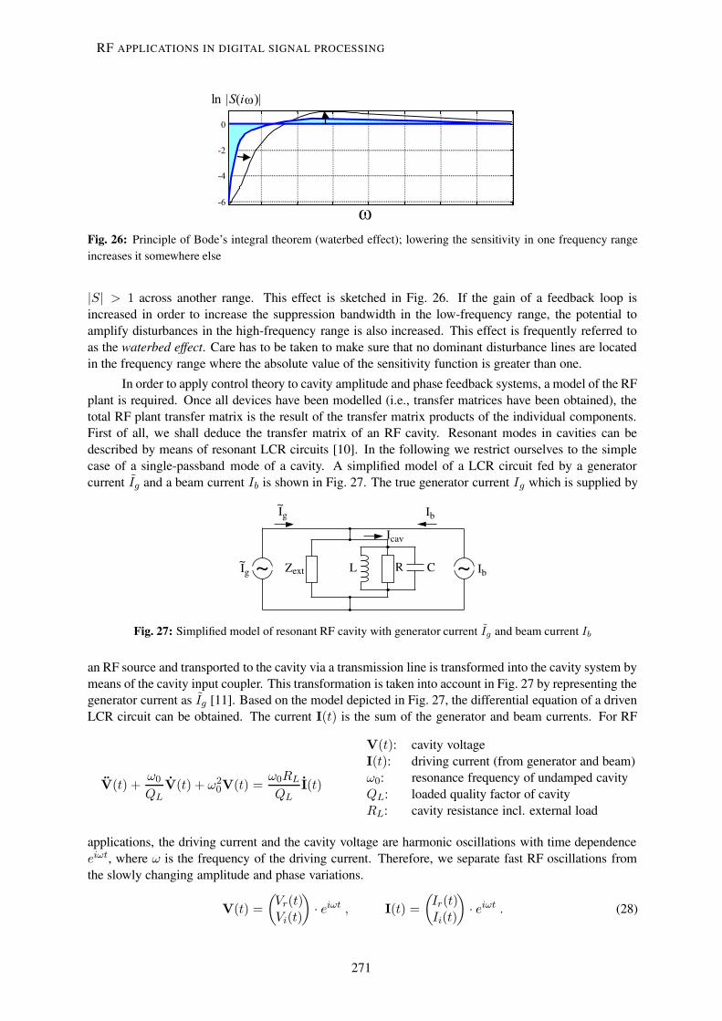
Fig. 26: Principle of Bode’s integral theorem (waterbed effect); lowering the sensitivity in one frequency rangeincreases it somewhere else
|S| > 1 across another range. This effect is sketched in Fig. 26. If the gain of a feedback loop isincreased in order to increase the suppression bandwidth in the low-frequency range, the potential toamplify disturbances in the high-frequency range is also increased. This effect is frequently referred toas the waterbed effect. Care has to be taken to make sure that no dominant disturbance lines are locatedin the frequency range where the absolute value of the sensitivity function is greater than one.
In order to apply control theory to cavity amplitude and phase feedback systems, a model of the RFplant is required. Once all devices have been modelled (i.e., transfer matrices have been obtained), thetotal RF plant transfer matrix is the result of the transfer matrix products of the individual components.First of all, we shall deduce the transfer matrix of an RF cavity. Resonant modes in cavities can bedescribed by means of resonant LCR circuits [10]. In the following we restrict ourselves to the simplecase of a single-passband mode of a cavity. A simplified model of a LCR circuit fed by a generatorcurrent Ig and a beam current Ib is shown in Fig. 27. The true generator current Ig which is supplied by
Fig. 27: Simplified model of resonant RF cavity with generator current Ig and beam current Ib
an RF source and transported to the cavity via a transmission line is transformed into the cavity system bymeans of the cavity input coupler. This transformation is taken into account in Fig. 27 by representing thegenerator current as Ig [11]. Based on the model depicted in Fig. 27, the differential equation of a drivenLCR circuit can be obtained. The current I(t) is the sum of the generator and beam currents. For RF
V(t) +ω0
QLV(t) + ω2
0V(t) =ω0RLQL
I(t)
V(t): cavity voltageI(t): driving current (from generator and beam)ω0: resonance frequency of undamped cavityQL: loaded quality factor of cavityRL: cavity resistance incl. external load
applications, the driving current and the cavity voltage are harmonic oscillations with time dependenceeiωt, where ω is the frequency of the driving current. Therefore, we separate fast RF oscillations fromthe slowly changing amplitude and phase variations.
V(t) =(Vr(t)Vi(t)
)· eiωt , I(t) =
(Ir(t)Ii(t)
)· eiωt . (28)
RF APPLICATIONS IN DIGITAL SIGNAL PROCESSING
271

In this formula, the notation of real and imaginary parts of the current and voltage have been choseninstead of the I and Q representation. Inserting Eq. (28) into the cavity differential equation results inthe description of the cavity field envelope as a matrix equation.
ddt
(VrVi
)=( −ω1/2 −∆ω
∆ω −ω1/2
)·(VrVi
)+(RLω1/2 0
0 RLω1/2
)·(IrIi
). (29)
The parameter ω1/2 is the cavity bandwidth of the loaded cavity, and ∆ω is the difference frequencybetween the resonance frequency and the frequency of the driving source. Both parameters are definedby
ω1/2 =ω0
2QL, ∆ω = ω0 − ω . (30)
In order to transform the differential Equation (29) into an algebraic equation, Laplace transformationcan be applied which yields(
Vr(s)Vi(s)
)︸ ︷︷ ︸V (s)
=ω1/2
∆ω2 + (s+ ω1/2)2
(s+ ω1/2 −∆ω
∆ω s+ ω1/2
)︸ ︷︷ ︸
Hcav(s)=
0@ H11(s) H12(s)H21(s) H22(s)
1A·(RL · Ir(s)RL · Ii(s)
)︸ ︷︷ ︸
U(s)
. (31)
Having done so, we have obtained the continuous 2×2 transfer matrix of a resonant cavity. A fewproperties of this matrix will now be highlighted. If the cavity is operated on resonance (∆ω = 0), thenthe off-diagonal elements of the transfer matrix vanish. The cavity acts like a low-pass filter of first orderwith a roll-off frequency of ω1/2.
∆ω = 0 (cavity on resonance) : H11(s) = H21(s) =ω1/2
s+ ω1/2(32)
H12(s) = H21(s) = 0 .
In this case, the real and imaginary parts of the cavity voltage (or the I and Q components), and thusamplitude and phase, are completely decoupled. If the cavity is detuned (∆ω 6= 0), coupling betweenI and Q occurs. Especially for superconducting cavities, which are subject to Lorentz force detuning athigh gradients, the cavity resonance frequency and therefore ∆ω becomes a function of the acceleratingfield in the resonator. If the cavity is operated in a pulsed mode, then the cavity filling causes a transitionof the resonance frequency. This leads to ∆ω = ∆ω(t). Thus the transfer functionHcav(s) becomes timevariant, therefore complicating the control task. The stability of the feedback loop has to be guaranteedunder these parameter changes, which may require modern control theory approaches to synthesize anoptimal controller.
As a next step, the transformation from the continuous into the discrete cavity model has to becarried out according to Eq. (24). Although an analytical expression of Hcav(z) could be given, thecalculation is tedious. Most of the time it is sufficient to use computer programs (octave, Scilab, matlab,etc.) and to analyse the feedback loop with its discrete transfer matrices. An alternative to using thetransfer matrix approach is the analysis of amplitude and phase feedback systems in the state spaceformalism [12] where the differential equation (29) can be written as
x(t) = A · x(t) + B · u(t) (33)y(t) = C · x(t) (34)
with the definitionx(t) =
(Vr(t)Vi(t)
), u(t) =
(Ir(t)Ii(t)
)
T. SCHILCHER
272

A =(−ω1/2 −∆ω
∆ω −ω1/2
), B =
(RLω1/2 0
0 RLω1/2
), C =
(1 00 1
).
In this lecture we shall not explore the approach of state space formalism in more detail. The transfermatrix analysis of the closed amplitude and phase feedback loop in the digital domain requires the loopdelay (which is inherent due to digital signal processing) to be taken into account. Also all cable delaysmust be considered. This delay of N sample periods is expressed by the z−N transfer matrix in Fig. 28.In most cases, the digital controller for amplitude and phase feedback for RF cavities is typically imple-
Fig. 28: Block diagram of a digital feedback loop with loop delay of N sample periods
mented using a PID controller. Nevertheless, studies are currently underway in many laboratories thataim at improving the feedback performance by synthesizing an optimal controller. Although PID con-trollers have been analysed thoroughly in many publications, we shall nevertheless investigate the loopperformance with this type of controller in more detail, since PID controllers play such an important rolein RF cavity field control. A standard PID control algorithm is expressed by
u(k) = u(k − 1) + (Kp +Ki +Kd) · e(k) − (Kp + 2Kd) · e(k − 1) +Kd · e(k − 2) (35)
with the error value e(k) at sample time tk, and the proportional, integral, and derivative gainsKp,Ki,Kd
respectively. To simplify matters, we regard the RF plant as consisting only of the cavity, neglecting allother components such as vector modulators, pre-amplifiers, klystrons, pickups, etc. Even with this sim-plified example, some important properties of the feedback design will be revealed. The plant G(z) inFig. 28 is described by the transfer function given in Eq. (31). As a standard rule of thumb, controltheory recommends a gain margin of at least between 6–8 dB and a phase margin of between 40◦ and60◦. With a constant integral gain (Ki = 0.1), the proportional gain is adjusted in the above-mentionedexample such that a gain margin of 8 dB is achieved. Depending on the total loop delay tD, differentmaximum proportional gains can be set which yield different loop bandwidths. The sensitivity functionas a result of this simulation is shown in Fig. 29. The achievable maximum bandwidth strongly dependson the total loop delay and is very sensitive if the total delay is on the order of the sampling period. Thusthe loop delay is an important parameter which has to be minimized. High-speed digital technology isrequired to keep the delay in the digital signal processing part as short as possible. However, despiteever more powerful digital technology, the larger delays typical of digital feedback systems (comparedto their analog counterparts) are still the limiting factor in their application. This becomes most evidentif superconducting and normal conducting cavity field feedback systems are compared (see Table 4). In
Table 4: Comparison of basic feedback parameters of normal and superconducting cavities
Superconducting cavity Normal conducting cavityQL: ≈ few 105–107 QL: ≈10–105
f1/2: ≈ few 100 Hz f1/2: ≈100 kHzτcav: ≈ few 100 µs τcav: ≈ few µsfeedback loop delay small compared to τcav feedback loop delay in the order of τcav
this table, the cavity bandwidth f1/2 is given by Eq. (30) and the cavity time constant (standing wavecavity) is the time constant of a resonator which is defined by
τcav =1
ω1/2=
QLπfRF
. (36)
RF APPLICATIONS IN DIGITAL SIGNAL PROCESSING
273

parameters:superconducting cavity with
f0 = 1.3 GHz,QL = 3 · 106,ω1/2 = 216 Hz,fs = 10 MHz;
controller: PI;integral gain: constant (Ki = 0.1);proportional gain: adjusted to keep
gain margin constant at 8 dB.
Fig. 29: Bode plot of the sensitivity function of a cavity-field feedback loop for different loop delays
Since the loaded quality factors QL of normal conducting cavities are some order of magnitudes smallerthan those of superconducting cavities, the bandwidths of the normal conducting cavities are usually inthe range of some hundred kHz. As a result, the cavity time constants are comparable with the loop delayswhich are typical of digital systems nowadays. The consequence is that loop gains are limited becauseunity gain is already reached with moderate gains at frequencies where the loop phase (dominated bythe phase advance of the loop delay) approaches 180◦. The achievable gains are highlighted in the openloop Bode plot (simplified model which consists of a series of cavity and loop delay transfer function) inFig. 30. If the bandwidth provided by a digital feedback system is insufficient, analog or analog/digital
Fig. 30: Open loop Bode plot of a normal conducting RF cavity for different loop delays
hybrid systems might offer an alternative. As a final example, a digital cavity amplitude and phasefeedback will now be shown. A schematic layout of the J-PARC LLRF system for the normal conducting
T. SCHILCHER
274

proton linac (Drift Tube Linac, DTL, and Separate-type Drift Tube Linac, SDTL) is depicted in Fig. 31[13, 14]. The linac is operated in pulsed mode with a repetition rate of 12.5 Hz or 25 Hz, respectively,
Fig. 31: Example of digital cavity amplitude and phase feedback system (J-PARC linac)
and a pulse length between 500 µs to 650 µs. One klystron feeds two drift tube structures. Samplingthe down-converted IF frequencies of 12 MHz with 48 MHz sampling frequency ADCs deliver a streamof I and Q data. The successive rotation matrices perform the 90◦ phase rotation, including an absolutephase shift, which accounts for the individual cable delays from the cavity pickups to the ADCs. Thedigital LLRF system calculates and controls the vector sum using a PI control algorithm. In addition,feed-forward is applied by means of lookup tables which are adapted from pulse to pulse. The cavityamplitude and phase control in the form of I/Q control is implemented in a single FPGA, while DigitalSignal Processors (DSPs) are used for tuner control, communication and configuration of the FPGA. Thenormal conducting cavities along the linac have loaded quality factors QL between 8 000 and 3 · 105 andtypical cavity time constants of around 100 µs due to the low operating frequency of 324 MHz. It hasbeen demonstrated that the required amplitude and phase stabilities of <±1% and <±1◦, respectively,have been superseded by a factor of six. The total loop delay amounts to about 500 ns and the loopbandwidth reaches 100 kHz with moderate proportional gains of 10 and integral gains of 0.01.
5.1.2 Radial and phase loopsBooster synchrotrons for hadron or ion acceleration are often designed to accelerate a variety of particleswith different charge-to-mass ratios. These machines must be able to capture and very often adiabaticallyrebunch the injected beam, and then accelerate it to the desired extraction energy. The different speciesof particles require very different acceleration cycles. The relation between the necessary magnetic fieldchange dB/B in a synchrotron, the change of the revolution frequency df/f , the change of the mean
RF APPLICATIONS IN DIGITAL SIGNAL PROCESSING
275

radial position dR/R and the relative particle energy γ is given by [15]
dB
B= γ2df
f+ (γ2 − γ2
tr)dR
R(37)
where γtr is the transition energy. The LLRF drive system must be very flexible and fast to supportthe dynamic changes throughout the ramp cycle. The beam control system’s task is to calculate therevolution frequency as a function of dipole field, control the cavity voltages, keep the mean radialposition of the beam on the desired value, and lastly, to maintain the synchronous phase Φs betweenbeam and cavity field. In addition, it must synchronize the RF phase to a master RF clock in order toprovide synchronization of the beam transport to other accelerator rings. The RF frequency can changeup to a factor of ten during the ramp. The values typically vary from several hundreds of kHz to severaltens of MHz. In order to support these large frequency changes, low Q cavities are used which are oftenferrite-loaded cavities or magnetic alloy based cavities. In contrast to electron machines, no dampingof synchrotron oscillations occurs in hadron machines. As a result, any particles deviating from thesynchronous phase Φs will lead to oscillations. Moreover, all errors due to phase noise, imperfectionsin the magnetic field B, power supply ripple, etc., will cause phase and radial errors of the acceleratedbeam with respect to their design values. Hence radial and phase loop feedback systems are required. Tosummarize, the beam control system consists of the following main components.
– Frequency programIt calculates the frequency based on the B field and based on desired radial position, it optimizesthe frequency ramp to improve injection efficiency, and it generates dual harmonic RF drive signalsfor cavities in order to provide bunch shaping capabilities.
– Beam phase loopIt forces the cavity RF phase to follow the beam phase, i.e., it maintains the synchronous phase.Thus it damps coherent synchrotron oscillations from injection errors (energy, phase), bendingmagnet noise, and low-frequency synthesizer phase noise.
– Radial loopIt keeps the beam to its design radial position during acceleration and therefore forces the beam tohave the synchronous energy.
– Cavity amplitude loopIt compensates for imperfections in the cavity amplifier chain and provides the capability to controlthe amplitude according to a ramping function.
– Synchronization loopIt locks the RF phase of the synchrotron to a master RF clock frequency in order to synchronizedifferent accelerator rings which in turn ensures proper beam transfer.
The required frequency signals were commonly generated by analog methods, mainly by mixers andvoltage controlled oscillators (VCOs), which were used to accommodate the large frequency changesduring the acceleration cycle. The disadvantage of VCOs is their lack of absolute accuracy. Theirstability limitations become evident if frequency tuning is necessary over a broad range. With the recentlarge advances in digital technology, VCOs were replaced more and more by Direct Digital Synthesis(DDS) in the late 1980s. The agility, reproducibility, and precision achieved with DDS supersedes theapplication of analog technology in most cases. Since DDS devices are completely digital except for theoutput DAC, their stability is completely defined by an external, highly stable fixed frequency oscillator.However, the spectral purity depends on the clock frequency and the operating frequency. After thedigital implementation of the frequency program, the phase and radial loops were also more and moreoften implemented as digital feedback systems. In recent years, fully digital beam control systems havebeen implemented at machines like LEIR, AGS, RHIC, etc. A basic system layout is shown in Fig. 32.All RF signals such as those from cavity pickups, phase pickups (e.g., Wall Current Monitor, WCM), and
T. SCHILCHER
276

Fig. 32: Basic structure of digital radial and phase loops for hadron/ion synchrotrons
from radial pickups (Beam-Position Monitor, BPM), are digitized by means of I/Q sampling or DigitalDown Conversion (DDC). The latter method is usually used since it provides the better possibility to trackthe changing frequencies as has been shown in Section 3.3. While the amplitude loop acts directly onthe amplitude of the drive signal, the radial and phase loop apply a correction to the calculated frequencyfrom the frequency program. The feedback gains of the purely digital control loops can be a function ofthe beam parameters in order to maintain the same loop performance throughout the acceleration cycle.To demonstrate this statement in more detail, the transfer functions of the radial and phase feedbackloops will now be examined. The open loop model of both feedback systems is depicted in Fig. 33 [16].The output of the DDS is amplified in a klystron and can be modelled in the simple case as a pure
Fig. 33: Open loop model of radial and phase loops in hadron/ion synchrotrons
amplification with factor k0. The transfer function of the broadband cavity is given in Eq. (32) (cavity onresonance) and is followed by the loop delay τ . It can be shown by beam dynamics calculation that thetransfer function from an RF frequency change ∆ωRF to beam phase difference ∆φB = φB(s)−φRF (s)is given by [16, 17]
HφB (s) =∆φB
∆ωRF=
s
s2 + ω2S
, (38)
which is based on the model of a lossless oscillation around the synchronous phase ΦS (linearized syn-chrotron oscillations). The frequency ωS is the synchrotron frequency and can be calculated to
ωS = frev ·√
2πeVRF cos ΦSh|η|E
,
where frev is the asymptotic revolution frequency, VRF the amplitude of the cavity voltage, h the har-monic number, E the particle energy, and |η| = |1/γ2 − 1/γ2
tr| with γtr the transition energy. Likewise,
RF APPLICATIONS IN DIGITAL SIGNAL PROCESSING
277

the transfer function from an RF frequency change ∆ωRF to a radial position change (or to the radialposition itself) can be modelled to
HR(s) =dR
∆ωRF=
b
s2 + ω2S
(39)
with b as a function of energy and synchronous phase.
b =ceVRF cos ΦS
2πβγtrE.
We shall not go further into the details of beam dynamic calculations here, but just emphasize that bothtransfer functions, HφB (s) and HR(s), are functions of energy which increases during the accelerationcycle. Hence the underlying model is time varying. These models are usually difficult to analyse and aretreated in the frame of Linear Parameter Varying (LPV) models. Controllers for LPV models are oftenscheduled, i.e., the controller parameters are adjusted over time to meet the changing plant dynamics andthus guarantee constant loop performance and stability. As an example, the implementation of a radialloop is shown in Fig. 34. It is a test system implementation for LEIR (Low Energy Ion Ring) which has
Fig. 34: Example of a radial loop implementation: LEIR system test at the PS Booster at CERN
been successfully tested at the PS Booster at CERN. Parts of the loop run on digital signal processors(feedback loop) while processing-intensive tasks like DDC have been implemented on FPGAs. Apartfrom the PI controller—which contains two different sets of control parameters (gain scheduling) tomatch the different parameters at injection and extraction—many of the concepts which have been pre-sented in this course have been applied. The frequency is calculated by the frequency program based onthe ‘B-train’ input, derived from a field measurement in a reference magnet which is connected in serieswith the bending magnets in the ring. Corrections from the radial and phase loop are added to the fre-quency output and applied to a Master DDS (MDDS). The distributed frequency is received by so-calledSlave DDS cards (SDDSs) which locally generate the RF drive frequency for their respective RF cavities.The signals from the beam-position monitor pickups (sum and difference signal) are down-converted byDDCs in which a 1st order CIC with decimation factor R = 64 has been implemented. Based on thedigitized sum and difference values (I ,Q), the position is calculated with a geometric scaling factor M .Finally, a NCO stage follows the PI controller.
T. SCHILCHER
278

5.2 Adaptive feed-forwardThe performance of RF feedback systems with repetitive or well-known errors can be improved by theapplication of adaptive feed-forward algorithms; the goal of these algorithms is to unburden the feedbackand/or to suppress known disturbances in advance. The use of feed-forward schemes to compensate beamloading in pulsed accelerating structures is a particularly common practice. The beam arrival time andduration is known in advance, but the induced voltage of the beam can only be compensated by feedbackafter a certain time, owing to the loop delay. Feed-forward systems have proven effective for suppressingthe transients which normally occur if only feedback is used. Since the repetitive disturbances can slowlyvary over time, the feed-forward signal has to be adapted by means of adaptive algorithms. The standardfeedback loop shown in Fig. 25 is extended by the adaptive feed-forward scheme (see Fig. 35). The
Fig. 35: Basic structure of an adaptive feed-forward in addition to a standard feedback loop
question remains as to how the feed-forward correction should be obtained. Recording the error signale(k), shifting it in time to compensate for the loop delay, then applying the opposite correction −e(k)will not work, since this approach does not take into account the plant dynamics. What is necessary is togenerate the proper additional input to the plant which then results in the required output −e(k). In otherwords, an inverse model of the plant is necessary to extract the input which leads to the output −e(k).However, this is not always easy in reality. A model to describe the dynamic behaviour of the system iseither not known or not precise enough. In addition, stochastic errors are superimposed on the measuredtotal error signal. Averaging methods are necessary in order to separate repetitive from stochastic errors.There are various approaches to attack this problem. One possibility is to obtain a system model bysystem identification (see Section 5.3), another way is to measure the system response with test inputsignals (step inputs), record the output, and calculate the system response matrix [18]. Assuming a lineartime-invariant Single Input–Single Output (SISO) system, an input u(k) = u(tk) will cause an outputy(k) = y(τk). Note that the definition of the sampling time is made such that the output occurs notearlier than
τk = tk + tD (40)due to the loop delay tD. If we change the input by small increments ∆u(tk) around the chosen workingpoint with input u(tk), the output changes by ∆y(τk) for linear systems (or for sufficient small changesin a first order approximation). The first change can be written as
∆y(τ1) = R11 ·∆u(t1) ,
where R11 describes the linear system response to the input ∆u(t1). The second sampled output changeis a linear combination of the previous two test input signals, expressed by
∆y(τ2) = R21 ·∆u(t1) +R22 ·∆u(t2) .
Applying successive test input signals ∆u(tk) to the system results in a sequence of output changeswhich can be written in a matrix equation. ∆y(τ1)
...∆y(τp)
=
R11 0... . . .
Rp1 . . . Rpp
· ∆u(t1)
...∆u(tp)
⇐⇒ ∆~y = R ·∆~u . (41)
RF APPLICATIONS IN DIGITAL SIGNAL PROCESSING
279
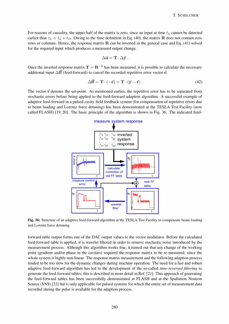
For reasons of causality, the upper half of the matrix is zero, since an input at time tk cannot be detectedearlier than τk = tk + tD. Owing to the time definition in Eq. (40), the matrix R does not contain zerorows or columns. Hence, the response matrix R can be inverted in the general case and Eq. (41) solvedfor the required input which produces a measured output change.
∆~u = T ·∆~y .
Once the inverted response matrix T = R−1 has been measured, it is possible to calculate the necessaryadditional input ∆~ff (feed-forward) to cancel the recorded repetitive error vector ~e.
∆~ff = T · (−~e) = T · (~y −~r) . (42)
The vector ~r denotes the set-point. As mentioned earlier, the repetitive error has to be separated fromstochastic errors before being applied to the feed-forward adaption algorithm. A successful example ofadaptive feed-forward in a pulsed cavity field feedback system (for compensation of repetitive errors dueto beam loading and Lorentz force detuning) has been demonstrated at the TESLA Test Facility (nowcalled FLASH) [19, 20]. The basic principle of the algorithm is shown in Fig. 36. The indicated feed-
Fig. 36: Structure of an adaptive feed-forward algorithm at the TESLA Test Facility to compensate beam loadingand Lorentz force detuning
forward table output forms one of the DAC output values to the vector modulator. Before the calculatedfeed-forward table is applied, it is wavelet filtered in order to remove stochastic noise introduced by themeasurement process. Although this algorithm works fine, it turned out that any change of the workingpoint (gradient and/or phase in the cavities) required the response matrix to be re-measured, since thewhole system is highly non-linear. The response matrix measurement and the following adaption processtended to be too slow for the dynamic changes during machine operation. The need for a fast and robustadaptive feed-forward algorithm has led to the development of the so-called time-reversed filtering togenerate the feed-forward tables; this is described in more detail in Ref. [21]. This approach of generatingthe feed-forward tables has been successfully demonstrated at FLASH and at the Spallation NeutronSource (SNS) [22] but is only applicable for pulsed systems for which the entire set of measurement datarecorded during the pulse is available for the adaption process.
T. SCHILCHER
280
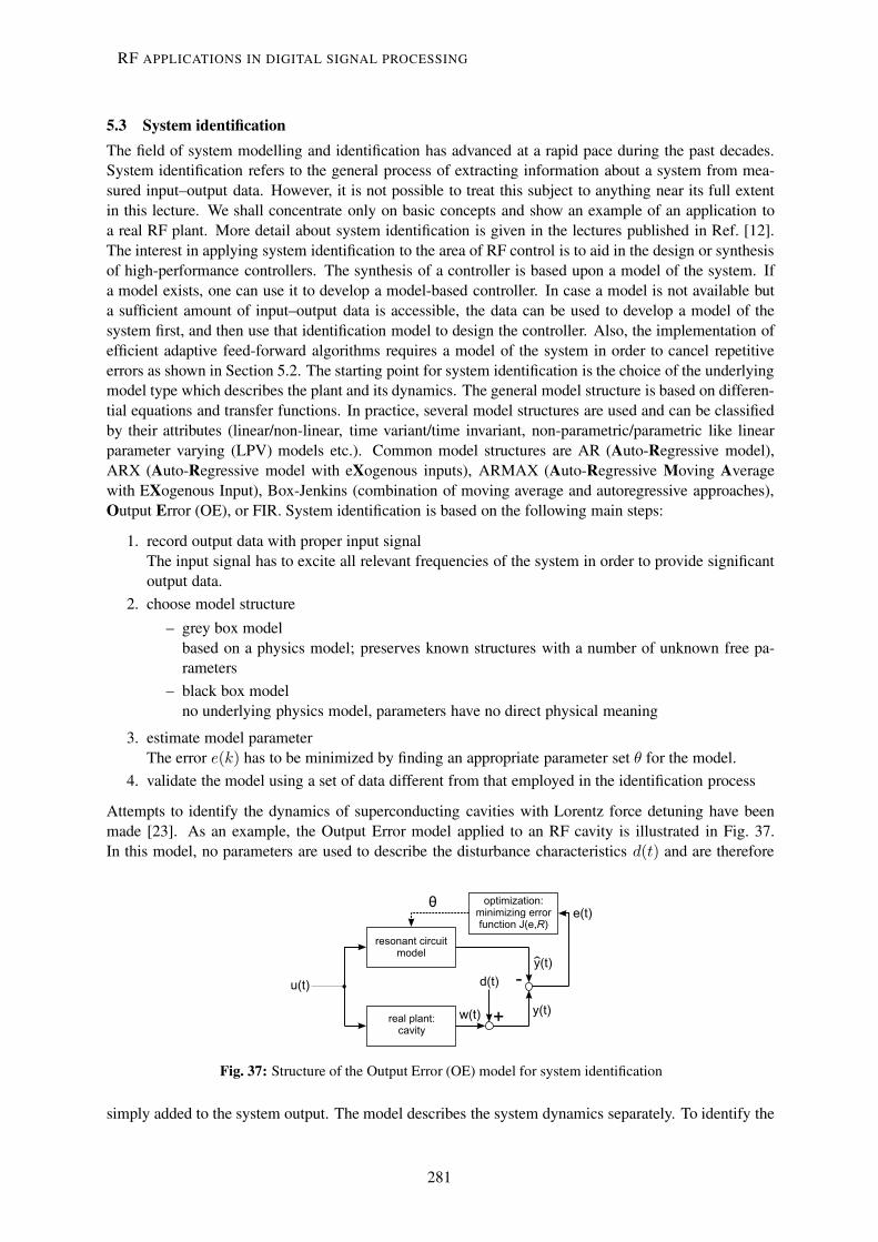
5.3 System identificationThe field of system modelling and identification has advanced at a rapid pace during the past decades.System identification refers to the general process of extracting information about a system from mea-sured input–output data. However, it is not possible to treat this subject to anything near its full extentin this lecture. We shall concentrate only on basic concepts and show an example of an application toa real RF plant. More detail about system identification is given in the lectures published in Ref. [12].The interest in applying system identification to the area of RF control is to aid in the design or synthesisof high-performance controllers. The synthesis of a controller is based upon a model of the system. Ifa model exists, one can use it to develop a model-based controller. In case a model is not available buta sufficient amount of input–output data is accessible, the data can be used to develop a model of thesystem first, and then use that identification model to design the controller. Also, the implementation ofefficient adaptive feed-forward algorithms requires a model of the system in order to cancel repetitiveerrors as shown in Section 5.2. The starting point for system identification is the choice of the underlyingmodel type which describes the plant and its dynamics. The general model structure is based on differen-tial equations and transfer functions. In practice, several model structures are used and can be classifiedby their attributes (linear/non-linear, time variant/time invariant, non-parametric/parametric like linearparameter varying (LPV) models etc.). Common model structures are AR (Auto-Regressive model),ARX (Auto-Regressive model with eXogenous inputs), ARMAX (Auto-Regressive Moving Averagewith EXogenous Input), Box-Jenkins (combination of moving average and autoregressive approaches),Output Error (OE), or FIR. System identification is based on the following main steps:
1. record output data with proper input signalThe input signal has to excite all relevant frequencies of the system in order to provide significantoutput data.
2. choose model structure– grey box model
based on a physics model; preserves known structures with a number of unknown free pa-rameters
– black box modelno underlying physics model, parameters have no direct physical meaning
3. estimate model parameterThe error e(k) has to be minimized by finding an appropriate parameter set θ for the model.
4. validate the model using a set of data different from that employed in the identification process
Attempts to identify the dynamics of superconducting cavities with Lorentz force detuning have beenmade [23]. As an example, the Output Error model applied to an RF cavity is illustrated in Fig. 37.In this model, no parameters are used to describe the disturbance characteristics d(t) and are therefore
Fig. 37: Structure of the Output Error (OE) model for system identification
simply added to the system output. The model describes the system dynamics separately. To identify the
RF APPLICATIONS IN DIGITAL SIGNAL PROCESSING
281

dynamics, the same inputs u(k) are applied to the model as to the real plant. The resulting differences inthe output e(t) = y(t) − y(t) are used to optimize the parameter set θ which describes the model. Thisis achieved by defining an error function with weighting matrix R. Apart from the goal of synthesizingan optimal controller and obtaining a model for feed-forward generation, system identification can alsogive insights about the system dynamics and provide information about not directly measurable states.Examples for these states are Lorentz force detuning ∆ω(t) during an RF pulse [see Eq. (29)], the beamphase with respect to the RF field, or the cavity bandwidth, which is mainly determined by the externalcoupling [24]. The principle of this approach is illustrated in Fig. 38. As is indicated, either the grey
Fig. 38: Example: system identification in pulsed high-gradient superconducting cavities with Lorentz force de-tuning
box model (based on the cavity model of a LCR circuit in conjunction with differential equations forthe Lorentz force detuning [25]) can be chosen, or a black box model is applied, in which case thedetermination of the appropriate model structure and order is typically a trial-and-error process.
6 ConclusionThe development of digital systems in the field of RF applications for accelerators has expanded sig-nificantly in the past decade due to the availability of greatly improved high-speed digital electronichardware. Fast feedback systems, which were usually the domain of analog systems, have been replacedmore and more by digital systems if the required regulation bandwidths are not too high. Digital low-levelRF systems have much in common with many other accelerator RF sub-systems such as beam diagnos-tics. Common platforms for both areas are possible, but with dedicated analog front-end electronics.The extensive diagnostics capabilities in digital RF systems allow the implementation of fully automatedprocedures and calibration schemes for those complex systems. Because of high flexibility and ease ofreconfiguration of software-based digital systems, more sophisticated algorithms than currently used areexpected to emerge in coming years.
References[1] M.E. Angoletta, Digital Low Level RF, EPAC’06, Edinburgh, Scotland, 2006, p. 1847.[2] R. Garoby, Low Level R.F. Building Blocks, CAS CERN Accelerator School, RF Engineering for
Particle Accelerators, Oxford, 1991, CERN–92–03, pp. 428–457.[3] M. Grecki, T. Jezynski and A. Brandt, Estimation of IQ Vector Components of RF Field - Theory
and Implementation, MIXDES 2005, Cracow, Poland, 2005, pp. 783–788.
T. SCHILCHER
282

[4] L. Doolittle, H. Ma and M.S. Champion, Digital Low-Level RF Control Using Non-IQ Sampling,LINAC’06, Knoxville, Tennessee, USA, 2006, p. 568.
[5] E. B. Hogenauer, An Economical Class of Digital Filters for Decimation and Interpolation, IEEETrans. Acoust. Speech Signal Process., vol. ASSP-29, no. 2, April 1981, pp. 155–162.
[6] M.E. Frerking, Digital Signal Processing in Communication Systems (Van Nostrand Reinhold, NewYork, USA, 1994).
[7] Xilinx Intellectual Property Center, datasheet, Cascaded Integrator-Comb (CIC) Filter, CaliforniaUSA, March 2002.
[8] B.F. Wu and E.A Jonckheere, A Simplified Approach to Bode’s Theorem for Continuous-Time andDiscrete-Time Systems, IEEE Trans. Autom. Control, vol. 37, Issue 11, Nov. 1992, pp. 1797–1802.
[9] B.F. Wu and E.A Jonckheere, Chaotic Disturbance Rejection and Bode Limitation, American Con-trol Conference, Chicago, Illinois USA, June 24–26, 1992, TP1, pp. 2227–2231.
[10] C.G Montgomery, R.H. Dicke and E.M. Purcell, Principles of Microwave Circuits, Radiation Lab-oratory Series Vol. 8 (McGraw-Hill, New York, 1942), Ch. 7.
[11] T. Schilcher, Vector Sum Control of Pulsed Accelerating Fields in Lorentz Force Detuned Super-conducting Cavities, DESY Print, TESLA 1998-20, 1998.
[12] S. Simrock, Lecture on Control Theory, these proceedings, 2007.[13] S. Michizono et al., Digital Feedback System for J-Parc Linac RF Source, LINAC’04, Luebeck,
Germany, 2004, p. 742.[14] S. Michizono et al., Performance of a Digital LLRF Field Control System for the J-PARC Linac,
LINAC’06, Knoxville, Tennessee, USA, 2006, p. 574.[15] J. Belleman, V. Chohan, J.L. Gonzalez, S. Johnston, E. Schulte and E. Thivent, Measurement of the
Mean Radial Position of a Lead Ion Beam in the CERN PS, EPAC’96, Sitges, Spain, 1996.[16] E. Onillon and J.M. Brennan, The New BNL AGS Phase, Radial and Synchronization Loops,
EPAC’96, Sitges, Spain, 1996.[17] D. Boussard, Design of a Ring RF System, CAS CERN Accelerator School, RF Engineering for
Particle Accelerators, Oxford, 1991, CERN–92–03, pp. 474–500.[18] R. Zhang, I. Ben-Zvi and J. Xie, A Self Adaptive Feedforward RF Control System for Linacs, Nucl.
Instrum. Methods Phys. Res. A324 (1993), pp. 421–428.[19] M. Liepe and S. Simrock, Adaptive Feed Forward for the Digital RF Control System at the TESLA
Test Facility, EPAC’98, Stockholm, Sweden, 1998, pp. 1735–1737.[20] M. Liepe, Regelung supraleitender Resonatoren mit Strahlbelastung am TESLA-Test-Linear-
beschleuniger, diploma thesis, University of Hamburg, 1998.[21] A. Brandt, Development of a Finite State Machine for the Automated Operation of the LLRF Control
at FLASH, PhD thesis, University of Hamburg, 2007.[22] H. Ma, private communication, ORNL, Tennessee USA, 2007.[23] G. Koch, Modelling of an Accelerator Based X-ray Free Electron Laser System for Controller
Design, diploma thesis, Technical University of Hamburg-Harburg, 2005.[24] S. Simrock, Digital Low-Level RF Controls for Future Superconducting Linear Colliders, PAC’05,
Knoxville, Tennessee USA, 2006, pp. 515–519.[25] M. Hüning, S. Simrock, System Identification for the Digital RF Control System at the TESLA Test
Facility, EPAC’98, Stockholm, Sweden, 1998, pp. 1732–1734.
RF APPLICATIONS IN DIGITAL SIGNAL PROCESSING
283