Review of Polyimides Used in the Manufacturing of Micro ... · Review of Polyimides Used in the...
16
April 2007 NASA/TM-2007-214870 Review of Polyimides Used in the Manufacturing of Micro Systems William C. Wilson Langley Research Center, Hampton, Virginia Gary M. Atkinson Virginia Commonwealth University, Richmond, Virginia https://ntrs.nasa.gov/search.jsp?R=20070018345 2018-07-05T03:40:00+00:00Z
-
Upload
dangnguyet -
Category
Documents
-
view
223 -
download
0
Transcript of Review of Polyimides Used in the Manufacturing of Micro ... · Review of Polyimides Used in the...
April 2007
NASA/TM-2007-214870
Review of Polyimides Used in the Manufacturing of Micro Systems William C. Wilson Langley Research Center, Hampton, Virginia
Gary M. Atkinson Virginia Commonwealth University, Richmond, Virginia
https://ntrs.nasa.gov/search.jsp?R=20070018345 2018-07-05T03:40:00+00:00Z

The NASA STI Program Office . . . in Profile
Since its founding, NASA has been dedicated to the advancement of aeronautics and space science. The NASA Scientific and Technical Information (STI) Program Office plays a key part in helping NASA maintain this important role.
The NASA STI Program Office is operated by Langley Research Center, the lead center for NASA’s scientific and technical information. The NASA STI Program Office provides access to the NASA STI Database, the largest collection of aeronautical and space science STI in the world. The Program Office is also NASA’s institutional mechanism for disseminating the results of its research and development activities. These results are published by NASA in the NASA STI Report Series, which includes the following report types:
• TECHNICAL PUBLICATION. Reports of
completed research or a major significant phase of research that present the results of NASA programs and include extensive data or theoretical analysis. Includes compilations of significant scientific and technical data and information deemed to be of continuing reference value. NASA counterpart of peer-reviewed formal professional papers, but having less stringent limitations on manuscript length and extent of graphic presentations.
• TECHNICAL MEMORANDUM. Scientific
and technical findings that are preliminary or of specialized interest, e.g., quick release reports, working papers, and bibliographies that contain minimal annotation. Does not contain extensive analysis.
• CONTRACTOR REPORT. Scientific and
technical findings by NASA-sponsored contractors and grantees.
• CONFERENCE PUBLICATION. Collected
papers from scientific and technical conferences, symposia, seminars, or other meetings sponsored or co-sponsored by NASA.
• SPECIAL PUBLICATION. Scientific,
technical, or historical information from NASA programs, projects, and missions, often concerned with subjects having substantial public interest.
• TECHNICAL TRANSLATION. English-
language translations of foreign scientific and technical material pertinent to NASA’s mission.
Specialized services that complement the STI Program Office’s diverse offerings include creating custom thesauri, building customized databases, organizing and publishing research results ... even providing videos. For more information about the NASA STI Program Office, see the following: • Access the NASA STI Program Home Page at
http://www.sti.nasa.gov • E-mail your question via the Internet to
[email protected] • Fax your question to the NASA STI Help Desk
at (301) 621-0134 • Phone the NASA STI Help Desk at
(301) 621-0390 • Write to:
NASA STI Help Desk NASA Center for AeroSpace Information 7115 Standard Drive Hanover, MD 21076-1320
National Aeronautics and Space Administration Langley Research Center Hampton, Virginia 23681-2199
April 2007
NASA/TM-2007-214870
Review of Polyimides Used in the Manufacturing of Micro Systems William C. Wilson Langley Research Center, Hampton, Virginia
Gary M. Atkinson Virginia Commonwealth University, Richmond, Virginia

Available from: NASA Center for AeroSpace Information (CASI) National Technical Information Service (NTIS) 7115 Standard Drive 5285 Port Royal Road Hanover, MD 21076-1320 Springfield, VA 22161-2171 (301) 621-0390 (703) 605-6000
Trade names and trademarks are used in this report for identification only. Their usage does not constitute an official endorsement, either expressed or implied, by the National Aeronautics and Space Administration.
Acronym List
(β-CN)/APB/ODPA (bis(aminophenoxy)benzonitrile)/AminoPhenoxy Benzene /OxiDiPhthalic Anhydride BPDA BenzoPhenonetetracarboxylic DiAnhydride CMUT Capacitive Micromachined Ultrasonic Transducer HF HydroFluoric LIGA LIthographie, Galvanoformung, Abformung
(German acronym for Lithography, Electroplating and Molding) MEMS MicroElectroMechanical Systems NMP N-Methyl-2-Pyrrolidone PDMS Poly-Di-Methyl-Siloxane PI PolyImide PMDA PyroMellitic DiAnhydride PMDA-ODA PyroMellitic DiAnhydride-OxyDiAniline PMMA Poly-Methyl-Meth-Acrylate PVDF PolyVinyliDene Dluoride RF Radio Frequency SAW Surface Acoustic Wave TFMOB TriFluoroMethOxyBenzidine UV Ultra-Violet VCU Virginia Commonwealth University
iii
1
Abstract
Since their invention, polyimides have found numerous uses in MicroElectroMechanical Systems (MEMS) technology. Polyimides can act as photoresist, sacrificial layers, structural layers, and even as a replacement for silicon as the substrate during MEMS fabrication. They enable fabrication of both low and high aspect ratio devices. Polyimides have been used to fabricate expendable molds and reusable flexible molds. Development of a variety of devices that employ polyimides for sensor applications has occured. Micro-robotic actuator applications include hinges, thermal actuators and residual stress actuators. Currently, polyimides are being used to create new sensors and devices for aerospace applications. This paper presents a review of some of the many uses of polyimides in the development of MEMS devices, including a new polyimide based MEMS fabrication process.
I. Introduction
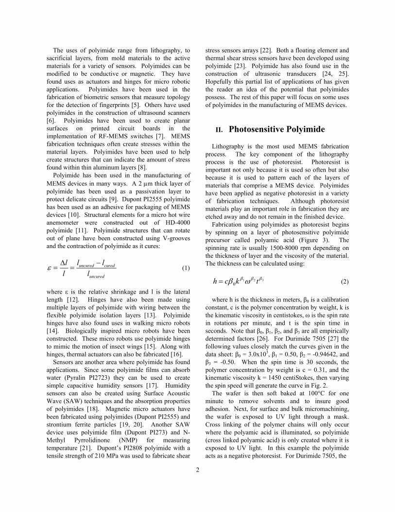
Polyimides have been around since the early 1960’s when they were invented by DuPont. Polyimides are thermosetting ring chain polymers that are constructed from imide monomers. See Figure 1 for the chemical structure of a typical PyroMellitic DiAnhydride-OxyDiAniline (PMDA-ODA) polyimide.
Polyimides are an extremely versatile material. They have a large degree of variability in their chemical make-up, and accept a wide variety of chemical additives. This allows for tailoring of the material properties to match the requirements of many different applications. They can be modified to be conductive or insulating, magnetic or non-magnetic, piezoelectric or non-piezoelectric, photosensitive or non-photosensitive as the user sees fit. With the addition of chemically specific additives, polyimides can be made to absorb specific chemical species, while remaining impervious to most other chemicals.
Figure 1. Chemical structure of a typical polyimide: PMDA-ODA.
Polyimides exhibit excellent chemical resistance. This is due to the concentration of polymer molecules which pack closely leaving very little room for solvents [1]. Polyimide materials have good dielectric properties. They exhibit a high resistance to radiation from both electrons and neutrons [2]. They are very stable both chemically and thermally; and are also durable and low cost [3]. Polyimides lend themselves to rapid fabrication techniques such as spinning, and they can be removed either isotropically or anisotropically rather quickly. Some of the properties of PMDA/BPDA/TFMOB polyimide useful in the manufacturing of MEMS devices are listed in Table I, from [4]. It is no surprise that they have found many applications in the fabrication of MicroElectroMechanical Systems (MEMS) devices. In fact, polyimide materials have been used in all phases of MEMS fabrication and operation.
TABLE I PROPERTIES OF PMDA/BPDA/TFMOB POLYIMIDE
PROPERTY Value Young's Modulus (in plane)
7.5 GPa
Young's Modulus (out of plane)
8.0-15.0 GPa
Shear Modulus 1.0-10.0 GPa Poisson's Ratio(in plane) 0.35 Poisson's Ratio (out of plane)
0.1-0.45
Dielectric coefficient 2- 4 Coefficient of thermal expansion
6.0x10⁻⁶ C-1
O
O N
C N
C
C
O O
C
O
nPMDA ODA
2
The uses of polyimide range from lithography, to sacrificial layers, from mold materials to the active materials for a variety of sensors. Polyimides can be modified to be conductive or magnetic. They have found uses as actuators and hinges for micro robotic applications. Polyimides have been used in the fabrication of biometric sensors that measure topology for the detection of fingerprints [5]. Others have used polyimides in the construction of ultrasound scanners [6]. Polyimides have been used to create planar surfaces on printed circuit boards in the implementation of RF-MEMS switches [7]. MEMS fabrication techniques often create stresses within the material layers. Polyimides have been used to help create structures that can indicate the amount of stress found within thin aluminum layers [8].
Polyimide has been used in the manufacturing of MEMS devices in many ways. A 2 "m thick layer of polyimide has been used as a passivation layer to protect delicate circuits [9]. Dupont PI2555 polyimide has been used as an adhesive for packaging of MEMS devices [10]. Structural elements for a micro hot wire anemometer were constructed out of HD-4000 polyimide [11]. Polyimide structures that can rotate out of plane have been constructed using V-grooves and the contraction of polyimide as it cures:
uncured
cureduncured
lll
ll #$
%$& (1)
where " is the relative shrinkage and l is the lateral length [12]. Hinges have also been made using multiple layers of polyimide with wiring between the flexible polyimide isolation layers [13]. Polyimide hinges have also found uses in walking micro robots [14]. Biologically inspired micro robots have been constructed. These micro robots use polyimide hinges to mimic the motion of insect wings [15]. Along with hinges, thermal actuators can also be fabricated [16].
Sensors are another area where polyimide has found applications. Since some polyimide films can absorb water (Pyralin PI2723) they can be used to create simple capacitive humidity sensors [17]. Humidity sensors can also be created using Surface Acoustic Wave (SAW) techniques and the absorption properties of polyimides [18]. Magnetic micro actuators have been fabricated using polyimides (Dupont PI2555) and strontium ferrite particles [19, 20]. Another SAW device uses polyimide film (Dupont PI273) and N-Methyl Pyrrolidinone (NMP) for measuring temperature [21]. Dupont’s PI2808 polyimide with a tensile strength of 210 MPa was used to fabricate shear
stress sensors arrays [22]. Both a floating element and thermal shear stress sensors have been developed using polyimide [23]. Polyimide has also found use in the construction of ultrasonic transducers [24, 25]. Hopefully this partial list of applications of has given the reader an idea of the potential that polyimides possess. The rest of this paper will focus on some uses of polyimides in the manufacturing of MEMS devices.
II. Photosensitive Polyimide
Lithography is the most used MEMS fabrication process. The key component of the lithography process is the use of photoresist. Photoresist is important not only because it is used so often but also because it is used to pattern each of the layers of materials that comprise a MEMS device. Polyimides have been applied as negative photoresist in a variety of fabrication techniques. Although photoresist materials play an important role in fabrication they are etched away and do not remain in the finished device.
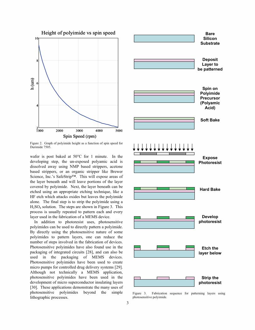
Fabrication using polyimides as photoresist begins by spinning on a layer of photosensitive polyimide precursor called polyamic acid (Figure 3). The spinning rate is usually 1500-8000 rpm depending on the thickness of layer and the viscosity of the material. The thickness can be calculated using:
321
0''' (' tkch $ (2)
where h is the thickness in meters, !0 is a calibration
constant, c is the polymer concentration by weight, k is the kinematic viscosity in centistokes, # is the spin rate in rotations per minute, and t is the spin time in seconds. Note that !0, !1, !2, and !3 are all empirically determined factors [26]. For Durimide 7505 [27] the following values closely match the curves given in the data sheet: !0 = 3.0x10³, !1 = 0.50, !2 = -0.94642, and !3 = -0.50. When the spin time is 30 seconds, the polymer concentration by weight is c = 0.31, and the kinematic viscosity k = 1450 centiStokes, then varying the spin speed will generate the curve in Fig. 2.
The wafer is then soft baked at 100°C for one minute to remove solvents and to insure good adhesion. Next, for surface and bulk micromachining, the wafer is exposed to UV light through a mask. Cross linking of the polymer chains will only occur where the polyamic acid is illuminated, so polyimide (cross linked polyamic acid) is only created where it is exposed to UV light. In this example the polyimide acts as a negative photoresist. For Durimide 7505, the
3
Spin Speed (rpm)
h (u
m)
1000 2000 3000 4000 50002
4
6
8
10Height of polyimide vs spin speed
Spin Speed (rpm)
h (u
m)
1000 2000 3000 4000 50002
4
6
8
10Height of polyimide vs spin speed
Figure 2. Graph of polyimide height as a function of spin speed for Durimide 7505.
wafer is post baked at 50°C for 1 minute. In the developing step, the un-exposed polyamic acid is dissolved away using NMP based strippers, acetone based strippers, or an organic stripper like Brewer Science, Inc.’s SafeStrip™. This will expose areas of the layer beneath and will leave portions of the layer covered by polyimide. Next, the layer beneath can be etched using an appropriate etching technique, like a HF etch which attacks oxides but leaves the polyimide alone. The final step is to strip the polyimide using a H2SO4 solution. The steps are shown in Figure 3. This process is usually repeated to pattern each and every layer used in the fabrication of a MEMS device.
In addition to photoresist uses, photosensitive polyimides can be used to directly pattern a polyimide. By directly using the photosensitive nature of some polyimides to pattern layers, one can reduce the number of steps involved in the fabrication of devices. Photosensitive polyimides have also found use in the packaging of integrated circuits [28], and can also be used in the packaging of MEMS devices. Photosensitive polyimides have been used to create micro pumps for controlled drug delivery systems [29]. Although not technically a MEMS application, photosensitive polyimides have been used in the development of micro superconductor insulating layers [30]. These applications demonstrate the many uses of photosensitive polyimides beyond the simple lithographic processes.
Figure 3. Fabrication sequence for patterning layers using photosensitive polyimide.
Bare Silicon
Substrate
Deposit Layer to
be patterned
Spin on Polyimide Precursor (Polyamic
Acid)
Expose Photoresist
Hard Bake
Develop photoresist
Etch the layer below
Soft Bake
Strip the photoresist
4
III. Polyimide as a sacrificial layer
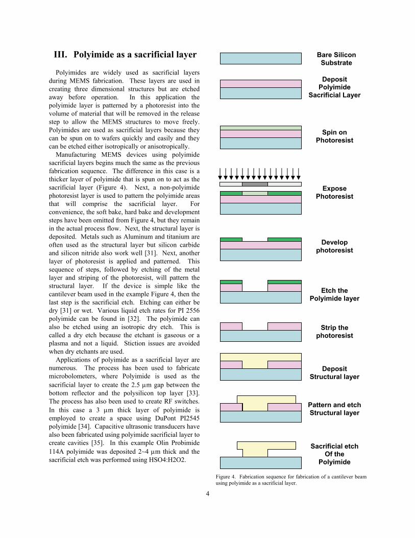
Polyimides are widely used as sacrificial layers during MEMS fabrication. These layers are used in creating three dimensional structures but are etched away before operation. In this application the polyimide layer is patterned by a photoresist into the volume of material that will be removed in the release step to allow the MEMS structures to move freely. Polyimides are used as sacrificial layers because they can be spun on to wafers quickly and easily and they can be etched either isotropically or anisotropically.
Manufacturing MEMS devices using polyimide sacrificial layers begins much the same as the previous fabrication sequence. The difference in this case is a thicker layer of polyimide that is spun on to act as the sacrificial layer (Figure 4). Next, a non-polyimide photoresist layer is used to pattern the polyimide areas that will comprise the sacrificial layer. For convenience, the soft bake, hard bake and development steps have been omitted from Figure 4, but they remain in the actual process flow. Next, the structural layer is deposited. Metals such as Aluminum and titanium are often used as the structural layer but silicon carbide and silicon nitride also work well [31]. Next, another layer of photoresist is applied and patterned. This sequence of steps, followed by etching of the metal layer and striping of the photoresist, will pattern the structural layer. If the device is simple like the cantilever beam used in the example Figure 4, then the last step is the sacrificial etch. Etching can either be dry [31] or wet. Various liquid etch rates for PI 2556 polyimide can be found in [32]. The polyimide can also be etched using an isotropic dry etch. This is called a dry etch because the etchant is gaseous or a plasma and not a liquid. Stiction issues are avoided when dry etchants are used.
Applications of polyimide as a sacrificial layer are numerous. The process has been used to fabricate microbolometers, where Polyimide is used as the sacrificial layer to create the 2.5 "m gap between the bottom reflector and the polysilicon top layer [33]. The process has also been used to create RF switches. In this case a 3 "m thick layer of polyimide is employed to create a space using DuPont PI2545 polyimide [34]. Capacitive ultrasonic transducers have also been fabricated using polyimide sacrificial layer to create cavities [35]. In this example Olin Probimide 114A polyimide was deposited 2~4 "m thick and the sacrificial etch was performed using HSO4:H2O2.
Figure 4. Fabrication sequence for fabrication of a cantilever beam using polyimide as a sacrificial layer.
Bare Silicon Substrate
Deposit Polyimide
Sacrificial Layer
Spin on Photoresist
Expose Photoresist
Develop photoresist
Etch the Polyimide layer
Strip the photoresist
Deposit Structural layer
Pattern and etch Structural layer
Sacrificial etch Of the
Polyimide
5
IV. Micro molding
Polyimide makes an excellent material for micro molds. Not only are they easy to deposit and pattern, but they are also durable and resilient to chemical and thermal degradation. It is for these reasons that polyimides have found application in high aspect ratio micro mold fabrication using LIGA techniques. The benefits of using polymers have also enabled the use of polyimides in technologies besides LIGA such as in expendable micro molds, and re-useable molds for contact printing.
A. LIGA High Aspect ratio devices using
Polyimides
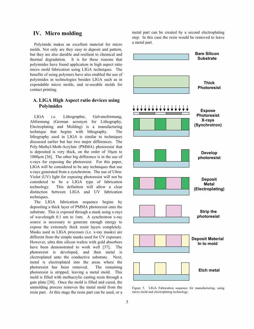
LIGA i.e. Lithographie, Galvanoformung, Abformung (German acronym for Lithography, Electroplating and Molding) is a manufacturing technique that begins with lithography. The lithography used in LIGA is similar to techniques discussed earlier but has two major differences. The Poly-Methyl-Meth-Acrylate (PMMA) photoresist that is deposited is very thick, on the order of 10µm to 1000µm [36]. The other big difference is in the use of x-rays for exposing the photoresist. For this paper, LIGA will be considered to be any techniques that use x-rays generated from a synchrotron. The use of Ultra-Violet (UV) light for exposing photoresist will not be considered to be a LIGA type of fabrication technology. This definition will allow a clear distinction between LIGA and UV fabrication techniques.
The LIGA fabrication sequence begins by depositing a thick layer of PMMA photoresist onto the substrate. This is exposed through a mask using x-rays of wavelength 0.1 nm to 1nm. A synchrotron x-ray source is necessary to generate enough energy to expose the extremely thick resist layers completely. Masks used in LIGA processes (i.e. x-ray masks) are different from the simple masks used for UV exposure. However, ultra thin silicon wafers with gold absorbers have been demonstrated to work well [37]. The photoresist is developed, and then metal is electroplated unto the conductive substrate. Next, metal is electroplated into the areas where the photoresist has been removed. The remaining photoresist is stripped, leaving a metal mold. This mold is filled with methacrylic casting resin through a gate plate [38]. Once the mold is filled and cured, the unmolding process removes the metal mold from the resin part. At this stage the resin part can be used, or a
metal part can be created by a second electroplating step. In this case the resin would be removed to leave a metal part.
Figure 5. LIGA Fabrication sequence for manufacturing, using micro mold and electroplating technology.
Bare Silicon Substrate
Thick Photoresist
Expose Photoresist
X-rays (Synchrotron)
Develop photoresist
Deposit Metal
(Electroplating)
Strip the photoresist
Deposit Material In to mold
Etch metal
6
For a standard LIGA process PMMA is the most common photoresist used, but often interest lies in the use of polyimide. When using polyimide as the photoresist, a thickness of 1000 µm can be obtained because photosensitive polyimide is 100 times more sensitive then PMMA [39]. This means that when using polyimide in a LIGA process, the radiation dosage of x-rays can be reduced by 100 times. This is very important because of the high costs associated with synchrotron operation.
B. Expendable molds
The hourly operating costs of LIGA techniques can be 8 times as much as the hourly costs for UV methods [40]. The high cost of LIGA fabrication, which is due to the high cost of synchrotron operation is the driving factor for the development of LIGA like techniques which use UV radiation instead of x-rays. Because polyimides have high sensitivity they have been investigated as a substitute for PMMA. High sensitivity is necessary when thick layers of photoresist are used. The fabrication sequence for expendable molds using polyimides is the same as is shown in Figure 5 for LIGA processing. The differences are that UV light is used instead of synchrotron generated x-rays and polyimide is used instead of the standard PMMA photoresist. The change of exposure sources causes a reduction in the thickness that can be achieved. This LIGA like process can yield a thickness of 3 to 150 µm for a single coat of polyimide [41]. Like the LIGA process the molds are filled using injection molding techniques and a gate plate [42].
C. Reusable flexible molds
Some applications do not require the destruction of the polyimide mold. To make reusable molds a process similar to the expendable mold process is used. A thick layer of polyimide is deposited and patterned using UV radiation. At this point the mold is complete. For contact printing the mold is filled with an inking material to be patterned in the printing process.
For some biomedical systems, polyimide molds are used as master molds to create molds out of Poly-Di-Methyl-Siloxane (PDMS) which is attached to a glass plate, cured, and then filled with the protein that is to be patterned [43]. Other biomedical applications involve the use of polyimide molds for transferring proteins and biological molecules such as neuroblastoma cells. The process begins with a double layer deposition of Dupont Pyralin 2611 polyimide 20
"m thick, next a layer of titanium is deposited and patterned to form a mask which is used in patterning the polyimide during an O2 plasma Reactive Ion Etch (RIE). This creates a grid from which an elastomer mold can be fabricated. The finished mold is filled with a protein and printed onto glass slides [44].
V. PolyMEMs Process
Aerospace applications require new light weight, low power sensors. Piezoelectric sensors have demonstrated a potential for many applications, but some require a material that is compatible with MEMS processing and has a wider temperature range than is currently available. The new process must be inexpensive, require few fabrication steps, and must not require overly complex tooling or hazardous chemicals. It is preferred that the new material have the same or better chemical resistance than that of PolyVinyliDene Dluoride (PVDF). It is also preferred that the new material not require stretching during the poling process as required for PVDF, because stretching is incompatible with most MEMS processes. After investigating existing fabrication techniques, the development of a new MEMS fabrication process for aerospace applications was found to be necessary. Polyimides are clearly very versatile because they can have tailored material properties. The material properties are controlled by the addition or substitution of the constituent chemicals. For example, piezoelectric properties can be introduced into polyimide materials. This led us to create the PolyMEMS process.
The Virginia Commonwealth University (VCU) has developed a polyimide manufacturing process called PolyMEMS [45] which uses a piezoelectric polyimide ((!-CN)/APB/ODPA) developed at the NASA Langley Research Center. This polyimide has greater potential for MEMS processing because it exhibits greater chemical resistance than that of flouropolymers such as PVDF [46]. Another reason for developing a new process is the limitation of PVDF, which does not function above 80ºC [47]. Electroactive (piezoelectric) polyimides have the potential of functioning at temperatures up to 150ºC.
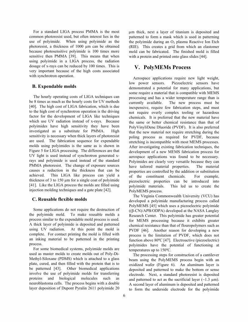
The processing steps for construction of a cantilever beam using the PolyMEMS process begin with an oxidized wafer (Figure 6). An aluminum layer is deposited and patterned to make the bottom or sense electrode. Next, a standard photoresist is deposited and patterned to act as the sacrificial layer (~1.3 µm). A second layer of aluminum is deposited and patterned to form the underside electrode for the polyimide
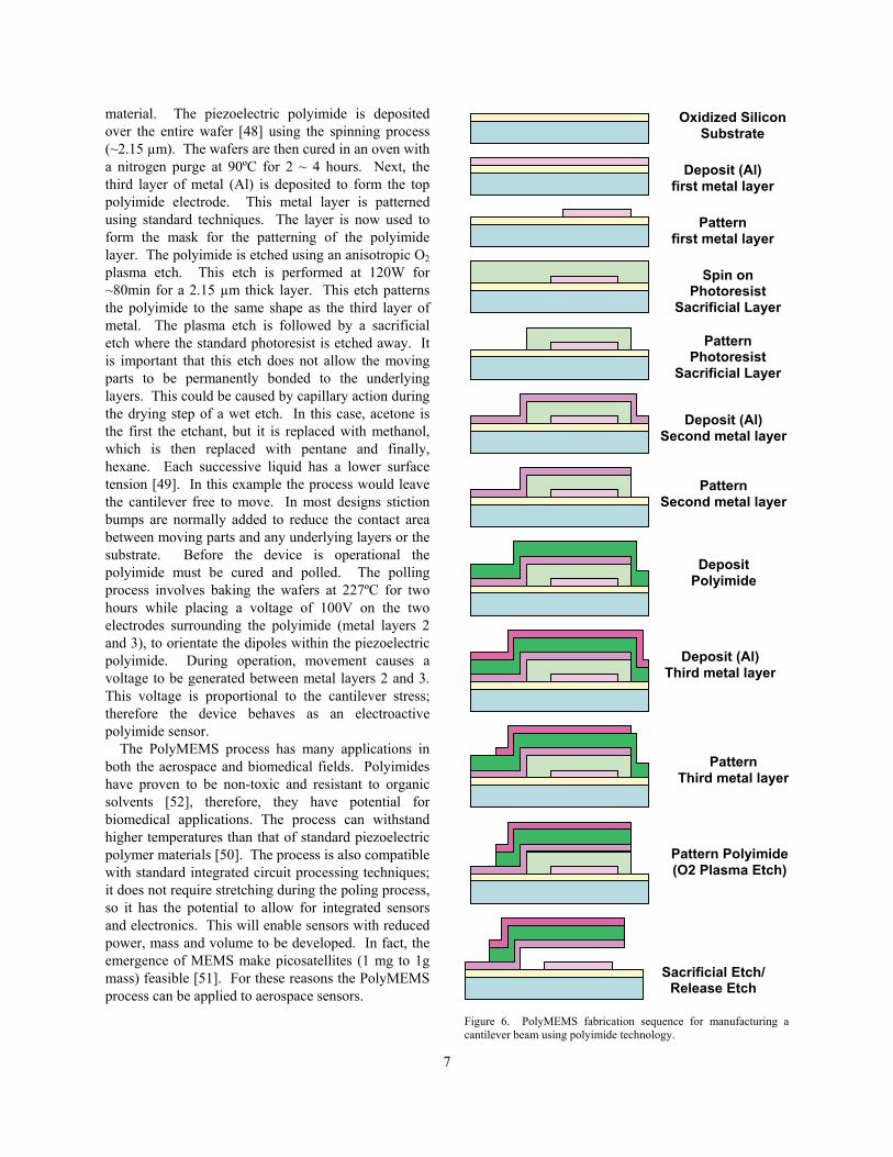
7
material. The piezoelectric polyimide is deposited over the entire wafer [48] using the spinning process (~2.15 µm). The wafers are then cured in an oven with a nitrogen purge at 90ºC for 2 ~ 4 hours. Next, the third layer of metal (Al) is deposited to form the top polyimide electrode. This metal layer is patterned using standard techniques. The layer is now used to form the mask for the patterning of the polyimide layer. The polyimide is etched using an anisotropic O2 plasma etch. This etch is performed at 120W for ~80min for a 2.15 µm thick layer. This etch patterns the polyimide to the same shape as the third layer of metal. The plasma etch is followed by a sacrificial etch where the standard photoresist is etched away. It is important that this etch does not allow the moving parts to be permanently bonded to the underlying layers. This could be caused by capillary action during the drying step of a wet etch. In this case, acetone is the first the etchant, but it is replaced with methanol, which is then replaced with pentane and finally, hexane. Each successive liquid has a lower surface tension [49]. In this example the process would leave the cantilever free to move. In most designs stiction bumps are normally added to reduce the contact area between moving parts and any underlying layers or the substrate. Before the device is operational the polyimide must be cured and polled. The polling process involves baking the wafers at 227ºC for two hours while placing a voltage of 100V on the two electrodes surrounding the polyimide (metal layers 2 and 3), to orientate the dipoles within the piezoelectric polyimide. During operation, movement causes a voltage to be generated between metal layers 2 and 3. This voltage is proportional to the cantilever stress; therefore the device behaves as an electroactive polyimide sensor.
The PolyMEMS process has many applications in both the aerospace and biomedical fields. Polyimides have proven to be non-toxic and resistant to organic solvents [52], therefore, they have potential for biomedical applications. The process can withstand higher temperatures than that of standard piezoelectric polymer materials [50]. The process is also compatible with standard integrated circuit processing techniques; it does not require stretching during the poling process, so it has the potential to allow for integrated sensors and electronics. This will enable sensors with reduced power, mass and volume to be developed. In fact, the emergence of MEMS make picosatellites (1 mg to 1g mass) feasible [51]. For these reasons the PolyMEMS process can be applied to aerospace sensors.
Figure 6. PolyMEMS fabrication sequence for manufacturing a cantilever beam using polyimide technology.
Oxidized Silicon Substrate
Deposit (Al) first metal layer
Spin on Photoresist
Sacrificial Layer
Deposit (Al) Second metal layer
Pattern first metal layer
Pattern Photoresist
Sacrificial Layer
Pattern Second metal layer
Deposit Polyimide
Deposit (Al) Third metal layer
Pattern Third metal layer
Pattern Polyimide (O2 Plasma Etch)
Sacrificial Etch/ Release Etch
8
VI. Conclusions and Outlook
This work presents the many uses of polyimides in the manufacturing of MEMS devices. Historically photosensitive polyimides have been used in MEMS processing techniques. This is mainly due do the fact that polyimides are easy to deposit, easy to etch both isotropically and anisotropically, and have many other benefits such as a low dielectric constant and thermal and chemical stability. These benefits also allow non-photosensitive polyimides to be used in many MEMS applications such as for structural and sacrificial layers. The desire for high aspect ratio devices drove the use of thick polyimide films that are UV curable as a method of creating molds much like those created using a standard LIGA process, but at a much reduced cost. A related technology uses polyimides to create flexible molds for imprinting. Humidity, temperature, magnetic, and ultrasonic sensors can be constructed using polyimides.
The versatility of polyimides has led us to develop a new fabrication process technique utilizing an electroactive polyimide. This new type of MEMS fabrication process (PolyMEMS) was presented. The use of this new process will allow for new sensor applications in harsh, high-temperature aerospace environments. This new process will enable a new class of polyimide sensors to be developed. One such device is the new type of ultrasonic sensor that can be constructed using electroactive polyimides. This device has the potential to become a low cost, Capacitive Micromachined Ultrasonic Transducer (CMUT) sensor for aerospace applications [53].
The outlook for polyimides in the future is very positive. As the progress on new materials and new polyimides continues, so will the development of new micro devices that employ polyimides. Researchers have yet to exploit all of the potential that exists in polyimides. Therefore, the future holds the promise of new and better devices, sensors, and actuators due in part to polyimides.
VII. References
[1] Wei Li, Jin-Li Zhang, Hui-Min Li, Tao Ding, Lin Wang, “Preparation of Ultrafiltration Membranes with Aromatic Polyimide”, 5th International Membrane Science & Technology Conference, Nov. 10 – 14, 2003, University of New South Wales, Sydney, Australia, paper no. 216, pp. 1 – 6.
[2] C. E. Sroog, A. L. Endrey, S. V. Abramo, C. E. Berr, W. M. Edwards, K. L. Olivier, “Aromatic Polypyromellitimides from Aromatic Polyamic Acids”, Journal of Polymer Science Part A: General Papers, Vol. 3, Issue 4, 1965, pp. 1373 – 1390.
[3] A. B. Frazier, “Recent Applications Of Polyimide to Micromachining Technology” Industrial Electronics, IEEE Trans. on, Vol. 42, Issue 5, Oct. 1995, pp. 442 – 448.
[4] B. Stark, “MEMS Reliability Assurance Guidelines for Space Applications” Brian Stark Editor, Jet Propulsion Laboratory, JPL Publication 99-1, Pasadena, California, pp. 49 - 67.
[5] N. Sato, S. Shigematsu, H. Morimura, M. Yano, K. Kudou, T. Kamei, K. Machida, “Novel Surface Structure and its Fabrication Process for MEMS Fingerprint Sensor”, Electron Devices, IEEE Trans. on, Vol. 52, Issue 5, May 2005, pp. 1026 – 1032.
[6] J. M. Zara, S. M. Smith, “A Micromachine High Frequency Ultrasound Scanner using Photolithographic Fabrication”, Ultrasonics, Ferroelectrics and Frequency Control, IEEE Trans. on, Vol. 49, Issue 7, July 2002, pp. 947 – 958.
[7] B. Ghodsian, Changwon Jung, B. A. Cetiner, F. De Flaviis, “Development of RF-MEMS Switch on PCB Substrates with Polyimide Planarization”, Sensors Journal, IEEE, Vol. 5, Issue 5, Oct. 2005, pp. 950 – 955.
[8] J. M. M. dos-Santos, K. Wang, A. B. Horsfall, et al., “Calibration of MEMS-Based Test Structures for Predicting Thermomechanical Stress in Integrated Circuit Interconnect Structures, Device and Materials Reliability, IEEE Trans. on, Vol. 5, Issue 4, Dec. 2005, pp. 713 – 719.
[9] J. Engel, J. Chen, and C. Liu, "Development of Polyimide Flexible Tactile Sensor Skin, "Journal of Micromechanics and Microengineering”, Vol. 13, No. 9, pp. 359-366, 2003.
[10] S.W. Park, K.S. Kim, J.B. Lee, and W.A. Davis, "Plastic-based Pattern Transfer Process for RF MEMS Passives", presented in 2002 IEEE Emerging Telecommunication Technologies Conference, Sep. 23 - 24, 2002, Dallas, TX.
9
[11] J. Chen, Z. Fan, J. Zou, J. Engel, and C. Liu, "Two Dimensional Micromachined Flow Sensor Array for Fluid Mechanics Studies," Journal of Aerospace Eng., Vol. 16, No. 2, pp. 85-97, 2003.
[12] T. Ebefors, J. Ulfstedt-Mattsson, E. Kälvesten, and G. Stemme, “3D Micromachined Devices based on Polyimide Joint technology”, SPIE Symposium on Microelectronics and MEMS, Gold Coast, Queensland, Australia, SPIE, Vol. 3892, October, 1999, pp. 118-132.
[13] H. Miyajima, N. Asaoka, M. Arima, Y. Minamoto, K. Murakami, and K. Matsumoto, “A Durable, Shock-Resistant Electromagnetic Optical Scanner with Polyimide-Based Hinges,” J. Microelectromech. Systems, Vol. 10, Sept. 2001, pp. 418–424.
[14] Thorbjörn Ebefors, Johan U. Mattsson, Edvard Kälvesten and Göran Stemme, “A Walking Silicon Micro-robot”, Presented at the 10th Int. Conference on Solid-State Sensors and Actuators (TRANSDUCERS99), Sendai, Japan, June 7-10, 1999, pp. 1202-1205.
[15] K. Suzuki, I. Shimoyama, and H. Muira, "Insect-Model Based Microrobot with Elastic Hinges," Journal of Microelectromechanical Systems, Vol. 3, No. 1, March 1994.
[16] T. Ebefors, J. U. Mattsson, E. Kalvesten, and G. Stemme “A Robust Micro Conveyer Realized by Arrayed Polimide Joint Actuators,” Journal of Micromechanics and Microengineering, Vol. 10, 2000, pp. 337-348.
[17] J. Laconte, V. Wilmart, D. Flandre, J.-P. Raskin, “High-Sensitivity Capacitive Humidity Sensor using 3-Layer Patterned Polyimide Sensing Film”, Sensors, 2003. Proceedings of IEEE, Vol. 1, Oct. 22-24 2003, pp. 372 – 377
[18] Manabu Sato, Tatsuo Yamamoto, Masao Takeuchi and Kazuhiko Yamanouchi, “Humidity Sensitivity of Lamb Waves on Composite Polyimide/ZnO/Si3N4 Structure“, Jpn. J. Appl. Phys. Special Issue: Ultrasonic Electronics, Vol. 32, May 1993, Part 1, No. 5B, pp. 2380-2383.
[19] L. K. Lagorce and M. G. Allen, “Magnetic and Mechanical Properties of Micromachined Strontium Ferrite/Polyimide Composites”, Journal of Microelectromechanical Systems, Vol. 6, No. 4, 1997, pp. 307-312.
[20] Jack W. Judy and Nosang Myung, “Magnetic Materials for MEMS”, MRS Workshop on MEMS Materials, San Francisco, California, (April 5-6, 2002), pp. 23-26.
[21] J. D. Sternhagen, C. E. Wold, W. A. Kempf, M. Karlgaard, K. D. Mitzner, R. D. Mileham, D. W. Galipeau,”A Novel Integrated Acoustic Gas and Temperature Sensor” Sensors Journal, IEEE, Vol. 2, Issue 4, Aug. 2002, pp. 301–306.
[22] F. Jiang, Y-C. Tai, K. Walsh, T. Tsao, G-B. Lee, C-M. Ho, “A Flexiblemems Technology and Its First Application to Shear Stress Sensor Skin” Proc. IEEE Int’l Conf. On MEMS, 1997, pp. 465-470.
[23] L. Löfdahl and M. Gad-el-Hak, “MEMS-Based Pressure And Shear Stress Sensors For Turbulent Flows”, Measurement Science and Technology, 1999, Vol. 10, pp. 665 – 686.
[24] Naoya Asamura, U. K. Saman Keerthi, Tatsuo Migita, Nobuyoshi Koshida, and Hiroyuki Shinoda, “Intensifying Thermally Induced Ultrasound Emission”, Proc. IEEE 19th Sensor Symposium, 2002, pp. 477-482.
[25] S. D. Glaser “Structural Health Monitoring Using High-Fidelity, Broadband, MEMS Displacement Sensors”, UCB/BSAC Abstract Proposal, found at www.ce.berkeley.edu/~glaser/MEMS-AE.pdf.
[26] W. A. Levinson, A. A. Arnold, O. Dehodgins, “Spin Coating Behavior of Polyimide Precursor Solutions”, Polymer Engineering and Science, Vol. 33, No.15, 1993, pp. 980-988.
[27] Fuji Film’s Durimide ® 7500 Series, Polyimide Negative Photoresist Data Sheet, Fuji Films Electronic Materials Inc., available at www.fujifilm-ffem.com/Products/Polyimides.aspx
[28] P. Cheang, G. Newmann, D. O. Murray, “An Optimized Process for Ultrathick Photosensitive Polyimide Applications,” Semicon/Taiwan IC Seminar, 1996, www.ultratech.com/pdf/ultathic.pdf.
[29] F. E. H., Tay, Choong, W.O., Liu, H., Xu, G.L., “An Intelligent Micro-Fluidic System for Drug Delivery”, Industrial Technology, Proceedings of IEEE International Conference on, Vol. 2, 19-22 Jan. 2000, pp. 70 – 75.
[30] K. Kikuchi, M. Goto, H. Nakagawa, S. Segawa, K. Tokoro, T. Taino, H. Myoren, S. Takada, M. Aoyagi, “Efficient Fabrication Process for Superconducting Integrated Circuits using Photosensitive Polyimide Insulation Layers”, Applied Superconductivity, IEEE Trans. on, Vol. 15, Issue 2, Part 1, June 2005, pp. 94 – 97.
[31] A. Bagolini, L. Pakula, T L. M. Scholtes, H. T. M. Pham, P. J. French, P. M. Sarro, “Polyimide Sacrificial Layer and Novel Materials for Post-Processing Surface Micromachining”, J. Micromech. Microeng. Institute Of Physics Publishing, Vol. 12, 2002, pp. 385–389.
[32] K. R. Williams, K. Gupta, and M. Wasilik, “Etch Rates for Micromachining Processing Part II,” Journal of Microelectromechanical Systems, Vol. 12, No. 6, Dec. 2003, pp. 761-778
10
[33] E. Mottin, A. Bain, J.-L. Martin, J.-L. Ouvrier-Buffet, S. Bisotto, J.-J. Yon, J.-L. Tissot, “Uncooled Amorphous Silicon Technology Enhancement for 25-um Pixel Pitch Achievement”, Infrared Technology and Applications XXVIII, Proceedings of SPIE, Vol. 4820, pp. 113-121.
[34] S. P. Pacheco, L. P. B. Katehi, C. T.-C. Nguyen, “Design of Low Actuation Voltage RF MEMS Switch”, Microwave Symposium Digest., IEEE MTT-S International, Vol. 1, June 2000, pp. 165-168.
[35] E. Cianci, D. Memmi, V. Foglietti, G. Caliano, and M. Pappalardo, “Capacitive Ultrasonic Transducers Fabricated by a Low Temperature Surface-Micromachining Process,” Precision Engineering, Vol. 26, Issue 4, 2002, pp. 347-354.
[36] W. Ehrfeld, P. Bley, F. Gotz, P. Hagmann, A. Maner, J. Mohr, H. O. Moser, D. Munchmeyer, W. Schelb, D. Schmidt, E. W. Baker, "Fabrication of Microstructures using the Liga Process", Proceedings of IEEE Micro Robots and Teleoperators Workshop, Hyannis, MA, Nov. 1987, pp.11/1-11/11, Reprinted in Micromechanics and MEMS: Classic and Seminal Papers to 1990, W. S. Trimmer Editor, January 1997, Wiley-IEEE Press, pp. 623-633.
[37] C. K. Malek, K. H. Jackson, W. D. Bonivert, and J. Hruby, “Masks for High Aspect Ratio X-Ray Lithography“, J. Micromech. Microeng., Vol. 6, June 1996, pp. 228-235.
[38] W. C. Tang, “Overview of Microelectromechanical Systems and Design Processes”, Technical Digest, 34th Design Automation Conference, June 9–13, 1997, Anaheim, California, pp 670–673.
[39] V. White, R. Ghodssi, C. Herdey, D. D. Denton and L. McCaughan, "Use of Photo-Sensitive Polyimide for Deep X-ray Lithography," Applied Physics Letters, Vol. 66, No. 16, April 17, 1995, pp. 2072-2073
[40] R. Lawes, “Microfabrication Cost Models for Micromachining Methods,” Materials & Packaging Challenges for Micro and Nano Technologies, Melbourne, Australia, Dec. 10, 2002, www.cmf.rl.ac.uk/pdf/aus2002.pdf.
[41] M. G. Allen, “Polyimide-Based Processes for the Fabrication of Thick Electroplated Microstructures,” 7th Int. Conf. Solid-State Sensors and Actuators, Yokohama, Japan, June 1993, pp. 60–65.
[42] G. Kovacs, “Micromachined Transducers Sourcebook”, McGraw Hill, NY, NY, 1998, pp. 133-138.
[43] T. Cornish, D. W. Branch, B. C. Wheeler, J. T. Campanelli, “Microcontact Printing: A Versatile Technique for the Study of Synaptogenic Molecules” Molecular and Cellular Neuroscience, Vol. 20, Issue 1, May 2002, pp. 140-153.
[44] B. C. Wheeler, D. W. Branch, J. M. Corey, J. A. Weyhenmeyer, and G. J. Brewer, "Engineering Neural Networks in Vitro: Microstamping Biomolecules to Control Cell Position," Engineering in Medicine and Biology society, 1997. Proceedings of the 19th Annual International Conference of the IEEE, Vol. 6, 30 Oct. 1997, pp. 2582 – 2585.
[45] G. M. Atkinson, W. C. Wilson, R. E. Pearson, Z. Ounaies, J. S. Harrison, C. Park and J. A Midkiff, "Piezoelectric Polyimide MEMS Process", Proceedings of NASA VLSI Symposium, May 2003.
[46] J. Simpson, Z. Ounaies and C. Fay, “Polarization and Piezoelectric Properties of a Nitrile Substituted Polyimide,” Mat. Res. Soc. Symposium Proc., Materials for Smart Systems II, Boston, MA, Nov. 1997, pp. 59-64.
[47] G. M. Atkinson, R. E. Pearson, Z. Ounaies, J. S. Harrison, C. Park, S. Dogan, and J. A Midkiff, "Piezoelectric Polyimide Tactile Sensor", Proceedings of the 15th Annual University/ Government/Industry Microelectronics Symposium, June 2003.
[48] G. M. Atkinson, R. E. Pearson, Z. Ounaies, J. S. Harrison, C. Park, S. Dogan, and J. A Midkiff, "Novel Piezoelectric Polyimide MEMS", Proce. of the 12th Annual Conf. on Solid-State Sensors, Actuators and Microsystems, June 2003.
[49] N. Tas, T. Sonnenberg, H. Jansen, R. Legtenberg, and M. Elwenspoek, “Stiction in Surface Micromachining,” J. Micromech. Microeng., Vol. 6, 1996, pp. 385–397.
[50] H. Helvajian, S. W. Janson, “Introduction to MEMS”, Microengineering Aerospace Systems, H Helvajian, AIAA, Reston VA, 1999, pp. 29-72.
[51] B. C. Lee, and W. J. Staszewski, “Modelling of Lamb Waves for Damage Detection in Metallic Structures: Part I Wave Prop.”, Smart Mater. Struct., Oct. 2003, Vol. 12, No. 5, pp. 804-814.
[52] R. R. J. Richardson, J. A. Miller, and W. M. Reichert, “Polyimides as Biomaterials: Preliminary Biocompatibility Testing,” Biomaterials, Vol. 14, No. 8, July 1993, pp. 627–635.
[53] W. C. Wilson, G. M. Atkinson, D. F. Perey, M. A. Scott, and K. K. Tedjojuwono, “Modeling of an Electroactive Polyimide Ultrasonic Wave Sensor for Aerospace Applications”, MSM 2005 Proc., Vol. 3, May 2005, Anaheim, CA, pp. 594 – 597.
REPORT DOCUMENTATION PAGE Form ApprovedOMB No. 0704-0188
2. REPORT TYPE Technical Memorandum
4. TITLE AND SUBTITLEReview of Polyimides used in the Manufacturing of Micro Systems
5a. CONTRACT NUMBER
6. AUTHOR(S)
Wilson, William C.; and Atkinson, Gary M.
7. PERFORMING ORGANIZATION NAME(S) AND ADDRESS(ES)NASA Langley Research CenterHampton, VA 23681-2199
9. SPONSORING/MONITORING AGENCY NAME(S) AND ADDRESS(ES)National Aeronautics and Space AdministrationWashington, DC 20546-0001
8. PERFORMING ORGANIZATION REPORT NUMBER
L-19339
10. SPONSOR/MONITOR'S ACRONYM(S)
NASA
13. SUPPLEMENTARY NOTESAn electronic version can be found at http://ntrs.nasa.gov
12. DISTRIBUTION/AVAILABILITY STATEMENTUnclassified - UnlimitedSubject Category 33Availability: NASA CASI (301) 621-0390
19a. NAME OF RESPONSIBLE PERSON
STI Help Desk (email: [email protected])
14. ABSTRACT
Since their invention, polyimides have found numerous uses in MicroElectroMechanical Systems (MEMS) technology. Polyimides can act as photoresist, sacrificial layers, structural layers, and even as a replacement for silicon as the substrate during MEMS fabrication. They enable fabrication of both low and high aspect ratio devices. Polyimides have been used to fabricate expendable molds and reusable flexible molds. Development of a variety of devices that employ polyimides for sensor applications has occured. Micro-robotic actuator applications include hinges, thermal actuators and residual stress actuators. Currently, polyimides are being used to create new sensors and devices for aerospace applications. This paper presents a review of some of the many uses of polyimides in the development of MEMS devices, including a new polyimide based MEMS fabrication process.
15. SUBJECT TERMSElectroactive Polyimide; MEMS; Polyimide; Polymer
18. NUMBER OF PAGES
1619b. TELEPHONE NUMBER (Include area code)
(301) 621-0390
a. REPORT
U
c. THIS PAGE
U
b. ABSTRACT
U
17. LIMITATION OF ABSTRACT
UU
Prescribed by ANSI Std. Z39.18Standard Form 298 (Rev. 8-98)
3. DATES COVERED (From - To)
5b. GRANT NUMBER
5c. PROGRAM ELEMENT NUMBER
5d. PROJECT NUMBER
5e. TASK NUMBER
5f. WORK UNIT NUMBER
136905.02.04.04.06
11. SPONSOR/MONITOR'S REPORT NUMBER(S)
NASA/TM-2007-214870
16. SECURITY CLASSIFICATION OF:
The public reporting burden for this collection of information is estimated to average 1 hour per response, including the time for reviewing instructions, searching existing data sources, gathering and maintaining the data needed, and completing and reviewing the collection of information. Send comments regarding this burden estimate or any other aspect of this collection of information, including suggestions for reducing this burden, to Department of Defense, Washington Headquarters Services, Directorate for Information Operations and Reports (0704-0188), 1215 Jefferson Davis Highway, Suite 1204, Arlington, VA 22202-4302. Respondents should be aware that notwithstanding any other provision of law, no person shall be subject to any penalty for failing to comply with a collection of information if it does not display a currently valid OMB control number.PLEASE DO NOT RETURN YOUR FORM TO THE ABOVE ADDRESS.
1. REPORT DATE (DD-MM-YYYY)04 - 200701-