Research and Infrastructure Development Center for ... · Research and Infrastructure Development...
63
1 ARMY RESEARCH LABORATORY Research and Infrastructure Development Center for Nanomaterials Research FINAL REPORT 15 AUG 2003 – 13 MAY 2009 Dr. Craig Friedrich ARL-CR-739 May 2009 Prepared by Michigan Technological University 1400 Townsend Drive Houghton, MI 49931 Under contract DAAD17-03-C-0115 DISTRIBUTION STATEMENT A. DISTRIBUTION IS UNLIMITED
Transcript of Research and Infrastructure Development Center for ... · Research and Infrastructure Development...

1
ARMY RESEARCH LABORATORY
Research and Infrastructure Development
Center for Nanomaterials Research
FINAL REPORT 15 AUG 2003 – 13 MAY 2009
Dr. Craig Friedrich
ARL-CR-739 May 2009
Prepared by
Michigan Technological University 1400 Townsend Drive Houghton, MI 49931
Under contract
DAAD17-03-C-0115
DISTRIBUTION STATEMENT A. DISTRIBUTION IS UNLIMITED

Report Documentation Page Form ApprovedOMB No. 0704-0188
Public reporting burden for the collection of information is estimated to average 1 hour per response, including the time for reviewing instructions, searching existing data sources, gathering andmaintaining the data needed, and completing and reviewing the collection of information. Send comments regarding this burden estimate or any other aspect of this collection of information,including suggestions for reducing this burden, to Washington Headquarters Services, Directorate for Information Operations and Reports, 1215 Jefferson Davis Highway, Suite 1204, ArlingtonVA 22202-4302. Respondents should be aware that notwithstanding any other provision of law, no person shall be subject to a penalty for failing to comply with a collection of information if itdoes not display a currently valid OMB control number.
1. REPORT DATE 01 MAY 2009
2. REPORT TYPE N/A
3. DATES COVERED -
4. TITLE AND SUBTITLE Research and Infrastructure Development Center for Nanomaterials Research
5a. CONTRACT NUMBER
5b. GRANT NUMBER
5c. PROGRAM ELEMENT NUMBER
6. AUTHOR(S) 5d. PROJECT NUMBER
5e. TASK NUMBER
5f. WORK UNIT NUMBER
7. PERFORMING ORGANIZATION NAME(S) AND ADDRESS(ES) Michigan Technological University 1400 Townsend Drive Houghton, MI 49931
8. PERFORMING ORGANIZATIONREPORT NUMBER
9. SPONSORING/MONITORING AGENCY NAME(S) AND ADDRESS(ES) 10. SPONSOR/MONITOR’S ACRONYM(S)
11. SPONSOR/MONITOR’S REPORT NUMBER(S)
12. DISTRIBUTION/AVAILABILITY STATEMENT Approved for public release, distribution unlimited
13. SUPPLEMENTARY NOTES The original document contains color images.
14. ABSTRACT
15. SUBJECT TERMS
16. SECURITY CLASSIFICATION OF: 17. LIMITATION OF ABSTRACT
UU
18. NUMBEROF PAGES
62
19a. NAME OFRESPONSIBLE PERSON
a. REPORT unclassified
b. ABSTRACT unclassified
c. THIS PAGE unclassified
Standard Form 298 (Rev. 8-98) Prescribed by ANSI Std Z39-18

2
The findings in this report are not to be construed as an official Department of Army position unless so designated by other authorized documents. Citation of manufacturer’s or trade names does not constitute an official endorsement or approval of the use thereof. DESTRUCTION NOTICE: for classified documents, follow the procedures in DoD 5220.22-M, National Industry Security Program Operating Manual, Chapter 5, Section 7. For unclassified, limited documents, destroy by any method that will prevent disclosure of contents or reconstruction of the document.

3
Research and Infrastructure Development
Center for Nanomaterials Research
FINAL REPORT 15 AUG 2003 – 13 MAY 2009
Submitted by Dr. Craig Friedrich
Michigan Technological University Department of Mechanical Engineering – Engineering Mechanics
Houghton, MI 49931 Phone: 906-487-1922 FAX: 906-487-2822
Email: [email protected]
Funding for the Center for Nanaomaterials Research at Michigan Technological University commenced on 15 August 2003 under Contract DAAD17-03-C-0115. The progress for the period in each of the thrust areas is detailed. Degrees granted, referred journal publications, refereed conference publications, and invention disclosures are listed with each of the thrust areas.
EXECUTIVE SUMMARY The research conducted under DAAD17-03-C-0115 “Research and Infrastructure Development Center for Nanomaterials Research” resulted in the research summaries contained within this report in addition to: 19 PhD degrees awarded or supported;
10 MS degrees awarded or supported;
36 Graduate students fully or partially supported;
43 Refereed Journal Publications;
2 Book Chapters;
79 Refereed Conference Publications and Presentations;
3 Invention disclosures;
1 Patent application.
Nanotechnology Circuit Design Using Single Electron Technology
The main objective of this research was to design and simulate nanotechnology circuits using single electron transistors. To this end, we have accomplished the following: • We have designed and simulated logic structures such as NOT, NOR and NAND gates based
on the Single Electron Transistors; • Novel 2- and 3-input NOR gate architectures were designed using SETs. Simulation results
were obtained by using both SIMON and SET-SPICE; • SET based NOR and NAND logic gates were designed using conventional CMOS circuit
architectures. The n- and p-type SET operations were achieved by biasing the control gate;

4
• The concept of hybrid circuits was extended to design a single-bit full adder; • Benchmarking has been performed by comparing the following technologies: a) Single stage
SET, b) N-SET with PMOS pull up, c) SET with amplifier output stage, and d) 70 nm CMOS technology;
• We began research into nanoscale interconnects by examining electrostatic capacitances offered by metallic carbon nanotubes in several interconnect configurations;
• Extraction of quantum capacitances for a multitude of carbon nanotube interconnects has been completed. Our calculations were performed for single walled metallic nanotubes for diameters ranging from 5 to 12 nm of both armchair and zigzag chiralities. Calculations were also performed on bundles comprised of these tubes.
Single Electron Transistor Device Technology Development
This research project has demonstrated room temperature single electron transistor (SET) devices through the development of focused ion beam (FIB) deposition and etch technologies. The five-year goal of this project task has been to characterize and employ FIB technologies for the demonstration and characterization of room temperature nanoscaled quantum electronic devices, specifically single electron transistors, which would lead toward higher levels of electronic and sensory integration to serve the mission of the U. S. military. The project has led to several notable accomplishments: • The first demonstration of operational room temperature metallic and semiconducting SET
devices fabricated by FIB technologies. This represents the sixth published worldwide demonstration of room temperature SET device operation;
• The first demonstration of arrays of hundreds of operational room temperature SET devices fabricated by nanoimprint lithography technology;
• The first characterization of FIB etching technologies to produce resolution-limited sub-17nm features in 30nm chromium films;
• The first demonstration of sub-10nm quantum dot array fabrication by FIB deposition technologies;
• The extension of orthodox SET device theory to model variations in quantum dot characteristics in a multi-dot array system.
Nano-To-Micro Interconnects
This research was focused both on the analytical and numerical study of dielectrophoretic assembly of metallic carbon nanotubes (CNTs) and on the experimental study of the process monitoring and control of dielectrophoretic assembly of a small number of multi-walled carbon nanotubes (MWNTs). • To study the effects and restrictive relations of the DEP parameters, a DEP model applicable
to CNT assembly and a simulation method based on this model were developed; • With simulation results, it is possible to optimize the process parameters of a CNT assembly,
specifically to determine the concentration of the CNT solution to accomplish a single CNT assembly;
• We performed real-time gap impedance monitoring of DEP assembly and sudden decreases of gap impedance signals corresponding to tube deposition were measured. The impedance

5
values agreed with the impedance model. Experiments confirmed that DEP assembly and measurement of gap impedance changes due to tube deposition can be accomplished with a single instrument, also providing a feedback signal for DEP process control;
• Based on the impedance model and the real-time gap impedance monitoring method, we demonstrated that a real-time gap impedance signal can be used to control a DEP process of MWNTs for assembly with a connecting resistance less than a defined limit, or for assembly with a defined number of connections.
Protein-Based Optical Nanosensors
The goal of this research was to begin development of a nanosensing technology platform using the optical protein Bacteriorhodopsin as the opto-electronic transduction medium and to integrate this material with standard and non-standard electronic devices. This work resulted in: • A method to extract and purify the protein from the cell membrane of the host bacterium; • Electrical characterization of the protein when deposited in oriented monolayers, oriented
patches, and un-oriented patches and the effects of optical bleaching; • A process and demonstration that the optical protein can be activated by bound quantum dots
and the activation can be modulated by resonant coupling; • A new method for lithographically patterning the functional protein, integration with CMOS
transistor gates, and demonstration of the operation of those transistors; • Integration and of the protein with operating single electron transistors and the electrical
characterization of the protein to assure minimal impact on the device performance; • Development of a process whereby an antibody protein, selected for a specific target antigen,
is bound to the optical protein and expressed in E. coli to replicate this fused sensor construct. Planar Magnetic Photonic Crystals for Integrated Photonic Devices
The primary goal was the development of high performance magnetic photonic crystals on chip and their application to integrated photonic devices. This research resulted in: • Deep-groove and highly efficient Bragg structures in magnetic garnet films were developed
and characterized; • Bandgaps and large polarization rotations in photonic crystal resonant cavities and at the band
edges were demonstrated; • Asymmetric photonic bandgap structures were developed and characterized; • Large sensitivity to variations in applied magnetic fields and cover refractive index were
demonstrated for sensor applications. Nano-scale Disordered Materials with Massive Functional Responses
The research activities of this group have been centered on understanding and manipulating materials with nano-scale compositional disorder that exhibit unusually extreme functional responses. The group has worked on developing and demonstrating cost-effective techniques for engineering massive responses to applied electric fields, magnetic fields, and temperature or electrochemical gradients in materials that have nano-scale compositional disorder.

6
The group was focused on four objectives: • Fabricate wafer-scale massively piezoelectric and electro-optic single-crystal (1-
x)Pb(Mg1/3Nb2/3)O3-(x)PbTiO3 (PMN-PT) oxide films on Al2O3 substrates; • Determine the ultimate limit on the magnetoelectric functionality that can be engineered in
metallic magnetostrictive Fe(1-x)Gax/piezoelectric PMN-PT heterostructures; • Engineer an unusually large thermoelectric figure of merit “ZT” in bulk AgPbmSbTe(2+m)
semiconductor materials (LAST alloys) using powder processing methods to efficiently generate electrical power from waste heat;
• Engineer low temperature fuel cell functionality in Gd0.1Ce0.9O(2-δ) (GDC) films.
Molecular Electronic Devices
The overall goal of this project was to explore the basic science and engineering issues for the fabrication of molecular electronic devices with stable carbon-carbon bonds between multiwalled carbon nanotubes (MWCNTs) and organic molecules. The investigation was guided by two possible device architectures. One is based on the horizontal crossing MWCNT configuration, and the other one is based on vertically aligned MWCNT arrays. Both configurations use MWCNTs as the nanoscale electrodes to connect functional molecules and the microelectrodes prepared by photolithography. • First success in preparing vertically-aligned multiwalled CNTs (MWCNTs) with the catalyst
particles (Ni) removed by post-synthesis acid etching; • Successfully integrate individual MWCNTs across the gaps of Ni microelectrodes. Liner
current-voltage (I-V) characters were obtained indicating effective Ohmic contacts; • Successfully prepared biphenyl molecules on planar carbon substrates by electrochemical
processes. Rectifying I-V behaviors were identified by STM; • Successfully functionalize MWCNTs with carboxylic groups as confirmed by specific
binding of Bovine serum albumin (BSA) labeled with fluorescent isothiocyanate.
The second goal of the project was to provide fundamental understanding of transport in devices based on molecules and nanostructures, prediction of novel nanostructures and study interaction of biological molecules with nanostructures. • The structural stability, electronic properties and chemical bonding of boron sheets and
nanotubes using first principles periodic approach was studied. The calculations predict the stability of a novel reconstructed 1221 sheet over the ‘idealized’ hexagonal 1212 sheet;
• The interaction of the DNA base molecules with graphene and carbon nanotubes was studied using density functional theory. We find that the equilibrium position is effectively conditioned by the combination of a weak van der Waals attractive force with a repulsive interaction between the π-orbital network in the five- and six-membered rings of the purine base and in the graphene sheet;
• With the aim of improving nanopore-based DNA sequencing, we explored the effects of functionalizing the embedded gold electrodes with purine and pyrimidine molecules. The results of our first-principles study indicate that this proposed scheme could allow DNA sequencing with a robust and reliable yield, producing current signals that differ by at least one order of magnitude for the different bases.

7
RESEARCH SUMMARIES
Nanotechnology Circuit Design Using Single Electron Technology Dr. Ashok K. Goel, Associate Professor, Co-PI Aranggan Venkataratnam (PhD 2008), Vidur Parkash (PhD in progress) Department of Electrical & Computer Engineering
The main objective of this research was to design and simulate nanotechnology circuits using single electron transistors. To this end, we have accomplished the following:
We have designed and simulated logic structures such as NOT, NOR and NAND gates based on the Single Electron Transistors. The capabilities of the simulator SIMON and SET-SPICE were studied. SIMON is based on the Orthodox theory and one of its limitations is that it ignores the effects of co-tunneling. The orthodox theory model can be implemented in different mathematical methods such as the Monte-Carlo method and the Master Equation method. Master equation approach is fast to simulate small circuits, however for increasing circuit size this method becomes highly complicated. SET-SPICE is a text-based model and can be used in any SPICE simulator. This model is based on the Master Equation approach. The major advantage of this simulator is that conventional electronic devices such as FETs can be combined with SET structures for simulation. Novel 2- and 3-input NOR gate architectures were designed using SETs. Simulation results were obtained by using both SIMON and SET-SPICE. Complementary operation was achieved by changing the background charge Q0 at the islands of the SETs. Initial simulations were performed at a temperature of 4.2 K. The island capacitance was about 10-21 F, which corresponds to a SET island size of about a nanometer. Switching of the transistors was achieved by the gate biases and the background charge, which control the number of electrons at the island. The effects of increasing the temperature, the island capacitance and the gate capacitance on the output waveforms were studied for the NOR gates. The rise and fall times of the output characteristics were also measured. SET based NOR and NAND logic gates were designed using conventional CMOS circuit architectures. The n- and p-type SET operations were achieved by biasing the control gate. The bias voltages were based on the current oscillations of a stand-alone SET. Expected simulation results were obtained when the SET island capacitances were about 10-19 F, which corresponds to an island size of about 2 nm. These SET sizes are typical of those reported in the literature. Effects of the operating temperature and the load capacitances were also studied. Analysis was done to increase the working temperature of SET’s. The problem was approached by first looking at current oscillations of the SET. The condition for observing single electron phenomenon is expressed as,
TKC
eE BC >>=
2
2
and 2
e
hRt >>

8
where e is the electronic charge, h is the Planck’s constant, C is the capacitance of the central island and T is temperature of the system. For room temperature operation substituting the value of T=300 K and KB, the value of Ec was found. Using the relation a capacitance of 10-19 F was used, which resulted in a period of 0.8 V. For this island and tunnel capacitances and Vdd = 20 mV, periodic oscillations of appropriate amplitude were seen with both SIMON and SET-SPICE models. The oscillation had amplitude of about 50 nA and showed switching characteristics. Using these biasing conditions, an inverter was designed and simulated at room temperature and appropriate results where obtained. This biasing was also extended to the NOR2 gate and its working was verified. The room temperature design was extended to simulate a NAND2 gate and the operation was verified. The rise and fall times of the CMOS based NOR2 gate were measured. Graduate student AV received training to use the FIB system. The training included the experience on the Nabity’s Nanometer Pattern Generation System. The limitations of circuit architecture on SIMON and SET-SPICE were explored. Graduate student AV worked with the fabrication team to characterize the FIB system. The smallest diameter for the central island of the SET that could be achieved by using the FIB system for etching is around 50 nm. However for room temperature operation, it is necessary to reduce the size of the central island further, to about 10 nm or less. One of the limitations of the single electron transistor circuits is its high output impedance. This results in loss of the signal during transfer of the signal from one stage of the circuit to the next stage. Also the single electron transistor provides very low gain. The fan out of the circuit is limited which also depends on the capacitance that is introduced by the following stage. In order to overcome these problems, a possible solution was to develop hybrid circuits combining both SETs and MOSFETs. The architecture included a SET logic stage and CMOS amplification cum driver stage. NOT, NOR and NAND logic circuits were simulated at room temperature using the hybrid architectures. These logic circuits worked at room temperature and the voltage levels of the simulated waveform at both the input and output were almost identical. The driving capability of the circuit was also improved. The concept of hybrid circuits was extended to design a single-bit full adder. Initially the CARRY bit and the SUM bit for a full-adder circuit were simulated individually. The output waveform for the CARRY bit and SUM bit were verified with standard CMOS full-adder operation. The SUM and CARRY bit circuits were integrated to make a full-adder circuit. The simulated results after the integration provided waveforms which verified a full-adder operation. Benchmarking has been performed by comparing the following technologies: a) Single stage SET, b) N-SET with PMOS pull up, c) SET with amplifier output stage, and d) 70 nm CMOS technology. The logic gates that were implemented using each of these technologies for benchmarking are NOT, NOR2, NAND2, XOR2, XNOR2 and SUM/CARRY BIT of a Full Adder. However in case of SET with the amplification stage only the SUM/CARRY BIT of a Full Adder was implemented. Each of these logic circuits had a 3 pF capacitance and a 10 MΩ resistance in parallel combination for the output load. Based on the benchmarking results, it seems that the SET-based circuits show a clear advantage in terms of the physical sizes, i.e., the amount of real estate occupied on the chip. The results also show that power consumption is the

9
lowest for single stage SET logic circuits. In terms of delay, CMOS-based circuits perform better than the SET circuits due to their higher current driving capability. The circuits employing N-SET with PMOS pull up show better delay performance compared to other SET circuits. The NSET/CMOS pull up circuit has Vout/Vin ratio for logic high equivalent to its CMOS counterpart. SET logic circuit with the amplification stage consumes the most amount of power and also needs two power supplies. As device dimensions scale down to the nanoscale dimensions, traditional interconnects are approaching a technological limit. Issues in dimensional control, grain and surface boundary scattering have given researchers good reasons for exploring alternate interconnect materials. Carbon nanotubes (CNTSs) have generated a lot of excitement in their potential role as interconnects in the scientific community. We have done explorations in performance measures of metallic carbon nanotubes as interconnects. Our focus has been to extract basic transmission line parameters of CNTs in order to create a simulation model for such interconnects. We began research into nanoscale interconnects by examining electrostatic capacitances offered by metallic carbon nanotubes in several interconnect configurations. We wrote our own code that employs the method of moments, a popular boundary element method to calculate electrostatic capacitances of different CNT interconnect configurations. We estimated capacitances of various CNT systems such as single walled nanotubes (SWNTs), multiwalled nanotubes (MWNTs) and single walled nanotube bundles. Capacitances were evaluated for single walled nanotubes and were compared with those for traditional metallic interconnects. It was found that the geometry of the nanotube gave it capacitance advantage over a metal interconnect with the same cross section. Capacitances of MWNTs effectively depended only on the external diameter of the tubes. The internal shells were effectively shielded by the outermost shell of the MWNT. Capacitances of multiwalled tubes were compared to those for SWNTs having the same outside dimensions as the outer shell of the MWNTs. We noted that the MWNTs exhibited 5-20% greater capacitance than the SWNTs within our range of calculations. Next, we focused on an evaluation of the quantum capacitances for CNT interconnect systems. The knowledge of these capacitances is an essential ingredient for developing a Gigahertz transport simulation model. Quantum capacitance is inherently dependent on the density of states function of the nanotube; hence a first principles calculation of their band structure was required. We have adopted the plane wave pseudo-potential method (PWPP) using ab-initio pseudo-potentials. Extraction of quantum capacitances for a multitude of carbon nanotube interconnects has been completed. Our calculations were performed for single walled metallic nanotubes for diameters ranging from 5 to 12 nm of both armchair and zigzag chiralities. Calculations were also performed on bundles comprised of these tubes. Our study indicates that the values of the Luttinger parameter “g” of the isolated tubes range from 0.08 to 0.3. These g-values seem to be consistent with experimentally obtained results on heterogeneous nanotube bundles. Between armchair and zigzag tubes, zigzag tubes show almost twice the quantum capacitance compared to the armchair varieties due to the presence of double degenerate bands at the Fermi level for the former. When compared to a single walled carbon nanotube, crystalline SWNT bundles show an enhanced electronic density-of-states at the Fermi level. This causes a large increase in quantum capacitances per unit cell when compared to an isolated single walled tube.

10
Degrees Awarded
• Aranggan Venkataratnam, PhD in Electrical Engineering 2008, Thesis titled Design and
Simulation of Logic Circuits Using Single Electron Transistors, Michigan Technological University.
• Vidur Parkash, PhD in Electrical Engineering 2008, Thesis titled Characterization of
Nanotube-Based Interconnects for Nanoscale Circuits, (in progress), Michigan Technological University.
Refereed Journal Publications
• Venkataratnam and A. K. Goel, "Design and Simulation of Logic Circuits with Hybrid Architectures of Single Electron Transistors and Conventional MOS Devices at Room Temperature," Microelectronics Journal, Vol. 39, No. 12, pp. 1461-1468, December 2008.
• Venkataratnam and A. K. Goel, "Design and Simulation of Logic Gates Using Single Electron Transistors at Room Temperature," International Journal of Computational Science
and Engineering, Vol. 2, Nos. 3/4, pp. 179-188, December 2006. • A. Venkataratnam and A.K. Goel, “Design and Simulation of Logic Circuits with Hybrid
Architectures of Single Electron Transistors and Conventional MOS Devices at Room Temperature,” Microelectronics Journal (under review).
Refereed Conferences Publications
• V. Parkash and A. K. Goel, “Characterization of Electrostatic Capacitances for Carbon Nanotube Interconnects,” Proceedings of the IEEE International Midwest Symposium on Circuits and Systems, Knoxville, Tennessee, August 10-13, 2008.
• V. Parkash and A. K. Goel, “Quantum Capacitance Extraction for Carbon Nanotube Interconnects,” CD-ROM Proceedings of the International Conference on Microelectronics, Sharjah, UAE, December 14-17, 2008.
• A. Goel and A. Venkataratnam, "Novel Designs of NOR2 and NOR3 Logic Gates Using Single Electron Transistors," Proceedings of the 2004 IEEE International Conference on
Semiconductor Electronics, December 7-10, 2004. • A. Venkataratnam and A. K. Goel, "CMOS Architectures for NOR and NAND Logic Gates
Using Single Electron Transistors," Technical Proceedings of the 2005 NSTI Nanotechnology
Conference, Vol. 3, pp 176-179, May 8-12, 2005. • A. Venkataratnam and A. K. Goel, "Design and Simulation of Logic Gates at Room
Temperature Using Single Electron Transistors," Proceedings of the 13th International
Workshop on the Physics of Semiconductor Devices, December 13-17, 2005. • A. Venkataratnam and A. K. Goel, “Simulation of Logic Circuits with Hybrid Architectures
of Single Electron Transistors and Conventional Devices,” CD-ROM proceedings, First
International Conference on Nano Networks, September 13-16, 2006. • A. K. Goel, “Designing Nanotechnology Circuits – The Interconnect Problem” Presented at
the Nano and Giga Challenges in Electronics and Photonics Conference, Phoenix, Arizona, March 12-16, 2007.

11
• A. K. Goel, “Nanotube and Other Interconnects for Nanotechnology Circuits” CD-ROM
Proceedings of the 21st Annual Canadian Conference on Electrical and Computer
Engineering, Niagara Falls, Ontario, Canada, May 4-7, 2008. • V. Parkash and A. K. Goel, “Electrostatic Capacitances for Carbon Nanotube Interconnects,”
IEEE Midwest Symposium on Circuits and Systems, Knoxville Tennessee, August 10-13, 2008. (Accepted).

12
Single Electron Transistor Device Technology Development Dr. Paul L. Bergstrom, Associate Professor, Co-PI Prasanjit Santosh Kumar Karre (Ph.D 2008), Daw Don Cheam (Ph.D candidate), Manoranjan Acharya (Ph.D candidate), Madhusudan Savaikar (Ph.D candidate), Aditya Kapoor (MSEE 2006). Department of Electrical & Computer Engineering.
Enabling Room Temperature Single Electron Transistor Devices
The successful outcome and demonstration of room temperature operation of metallic and semiconducting single electron transistors under this project would not be possible without the significant research and characterization of the focused ion beam instrument employed to create the device structures. The Hitachi FB-2000A focused ion beam instrument utilized for this program, coupled with the Nabity ion beam controller system, has allowed broad exploration of the process parameters necessary to characterize the finest etched line feature and the most uniform sub-10nm deposited quantum dots. Beam energy, ion flux density, and beam profile have been extensively modeled and characterized to enable the research team to specifically explore the limits of focused ion beam technology. Monte Carlo modeling of beam energy and profile, coupled with experimental verification, has yielded optimal etch and deposition parameters fundamentally required to produce the few nanometer features necessary for SET devices. Examples of these etched and deposited features are shown in the micrographs in Fig. 1 and Fig. 2. These technological developments enable the required features and structural profiles for nanoscaled quantum electronic devices of many types.
Figure 1: Top view FE-SEM micrograph
of sub-20nm FIB etched features in
20nm thick Cr electrodes.
Figure 2: Top view FE-SEM micrograph of
sub-10nm tungsten quantum dots
formed by FIB deposition.
The development of etch and deposition processes to enable nanometer scale features required in quantum electronic devices is significant. Merging the processing required for uniform production of quantum tunneling barriers, and the localization of quantum dots in the gap between electrodes in a consistent process integration, coupled with the requirement to explore many operational geometries of SET devices has been a significant challenge in the realization of

13
operational room temperature SET devices. The production of a uniform chemical oxidation of the tungsten quantum dots was key to developing a functional device, and the sequence in which that process was performed has been identified as a key component in successful versus failed device operation. The characterization of this oxide tunnel barrier was performed and indicated sufficient barrier height to enable electron localization on a quantum dot at room temperature. A cross sectional FE-SEM micrograph of the oxidized tungsten quantum dot is shown in Fig. 3. The process was optimized to tailor the tunneling barrier width and quantum dot dimension.
Figure 3: Cross sectional FE-SEM
micrograph of chemically oxidized
tungsten quantum dots.
Figure 4: UV-NIL patterned SET device
electrodes with 37nm source-drain
gap spacing.
Nanometer scale patterning has been performed by two means under this project: direct FIB etching and by ultraviolet nanoimprint lithography (UV-NIL). These technologies must be integrated appropriately for success. The micrograph of Fig. 1 demonstrates a narrow gap SET by FIB technology for a planar SET device structure. The current feature limit developed under this project is 11nm. Due to the serial write nature of the FIB direct patterned SET device, the exploration of alternatives to bring this process to large scale processing was necessary. The nanoimprint lithography technique demonstrated a suitable pathway to large-scale integration of nanometer features for parallel processing of thousands to millions of devices at a time. A micrograph image of the UV-NIL processed SET electrodes is shown in Fig. 4 demonstrating 37nm features suitable for room temperature operation.

14
Demonstrating Room Temperature Single Electron Transistor Devices
Figure 5: Room temperature operating
SET device by FIB technologies.
Figure 6: Room temperature operating
SET devices by NIL technology.
Integrating the processes and requirements, Figures 5 and 6 give examples of operational room temperature single electron transistor devices by focused ion beam and nanoimprint technologies. Demonstrating functionality and characteristic Coulomb blockade and Coulomb oscillations at room temperature, the project achieved its five-year goal to demonstrate functional single electron transistors by focused ion beam technologies. Figure 7 demonstrates the device characterization of a SET device showing output conduction versus source drain bias for different control gate biases of a device with silicon quantum dots fabricated in a modified process flow. The difference in the two curves shows strong gate control of the output behavior at room temperature for these devices. The modulation of the Coulomb blockade with gate bias also demonstrates strong control of the output behavior. Figure 8 shows the characteristic Coulomb oscillations for this same Si SET device showing well-behaved and periodic oscillations. The behavior for devices with different gap spacing as well as gate spacing does modify the characteristics for the SET, and this aspect of the device characterization is less well understood and documented in the literature. While these multi-dot metallic and semiconducting SET devices demonstrate clear and characteristic single electron behavior at room temperature, existing orthodox SET theory cannot fully explain the behavior for multi-dot devices. This lack of suitable modeling has led to an effort to more fully explain the quantum behavior of these devices at room temperature.

15
-4 -2 0 2 4
-250
-200
-150
-100
-50
0
50
100
150
200
250D
rain
Curr
en
t Id
in
pA
Vds in Volts
Vg=25mV
Vg=0mV
0.00 0.05 0.10 0.15 0.20 0.25 0.30
8.5
9.0
9.5
10.0
10.5
Dra
in c
urr
en
t in
pA
Vate voltage Vg in volts Figure 7: Vsd vs. Id characteristic of a SET
with Si quantum dots showing a
narrow but pronounced Coloumb
blockade profile at room temperature
and strong gate modulation of
current.
Figure 8: Vgs vs. Id characteristic of a SET
with Si quantum dots showing
characteristic periodic and well
behaved Coulomb oscillations at
room temperature.
The modeling of the multi-dot SET structure has been initiated by coupling the existing orthodox theory for SET operation presented by Likharev and others with the need to represent process variation in position, spacing, and dimension for a multidimensional array of quantum dots that could potentially participate in the quantum conduction. A Kinetic Monte-Carlo (KMC) simulation approach has been used initially to model the V-I characteristics of the SET device. The parameters like the dot dimension and the inter-dot spacing represent the nominal values for the physical devices. All possible tunneling events are considered by the KMC, which, together with the tunneling rates determine the current flowing through the device. The inter-dot tunneling rate is determined using the orthodox theory. Weaknesses in the current approach are represented by errors that were introduced in the calculations while inverting the capacitance matrix. These weaknesses are directly reflected in a deviation from the experimental V-I characteristics by two orders of magnitude below expected values, as demonstrated in Fig. 9. Key efforts currently being explored are to understand and define the fundamental questions involved in the interdependence of the electron tunneling rate and the probability of electron’s presence on the dot in the case of two mesoscopic tunnel junctions coupled in a series.
Figure 9: Model output showing Coulomb
blockade for a small 2-D array of
quantum islands to test the quality of
the model framework.

16
Challenges Raised by the Room Temperature SET Development
Many technological hurdles were surmounted in the research performed under this project task. The characterization and utilization of focused ion beam deposition and etch technologies were foundational to enabling the demonstration of functional room temperature quantum electronic devices. The technology functions and was successfully integrated into a process flow. The devices function at room temperature and required and have characteristic behavior representative of SET operation. The behavior of the processes and of the devices can be modeled using existing theories and methods. However, there is very much we still do not understand, and very much still remaining to accomplish for these devices to be utilized as they could be for future generations of highly integrated electronic and sensing systems.
Several key areas of research are needed to take these technologies to useful function in electronic and sensing systems. First, the theory and modeling of SET device behavior is very limited when applied to room temperature operation especially of multi-dot devices. Because of the complexity of the system, the orthodox theory cannot model real device behavior accurately due to its fundamental underlying assumptions, nor can it account for topological options for the SET that have been explored in this research. A more complete model accounting for three-dimensional field and quantum mechanical interactions is still needed. Second, the exploration of the integration of SET devices with mainstream CMOS was initiated in this research project, but was not broadly explored to understand the challenges and potential level of integration possible for these potentially compatible device platforms. Third, characterizing the impact of three-dimensional geometry on SET behavior is needed, and coupled with the background theory defined in the first research challenge.
The SET is a potentially useful tool in the integration of electronic and sensory systems. Its electrometer-like behavior is ideal to couple with ultra small sensory systems and its extraordinarily small device topology and potential for multidimensional integration with existing electronic platforms could lead to extraordinary levels of device integration in the future.
Degrees Awarded
• Prasanjit Santosh Kumar Karre, Ph.D in Electrical Engineering, February 2008. Thesis titled, Fabrication and Characterization of Room Temperature Operating Single Electron
Transistors by Focused Ion Beam Technologies, Michigan Technological University. • Aditya Kapoor, MS in Electrical Engineering, September 2006. Thesis titled, Thin Film
Tunnel Junctions for Single Electron Transistors, Michigan Technological University.
Refereed Journal Publications
• P. S. K. Karre, M. Acharya, W. R. Knudsen, and P. L. Bergstrom, “Single Electron Transistor based Gas Sensing with Tungsten Nano Particles at Room Temperature,” IEEE
Sensors Journal, vol. 8(6) (2008) pp. 797 – 802. • P. S. K. Karre, P. L. Bergstrom, G. Mallick, and S. P. Karna, “Room Temperature
Operational Single Electron Transistor Fabricated by Focused Ion Beam Deposition,” J.
Applied Physics, vol. 102 (2007) 024316.

17
Refereed Conference Publications
• P. Santosh Kumar Karre, Paul L. Bergstrom, Govind Mallick, and Shashi P. Karna, “Observation of Coulomb Blockade at Room Temperature using an Array of Tungsten Nano Islands,” Digest 2007 Nanoelectronic Devices for Defense & Security (NANO-DDS’07), Paper # 192, Crystal City, VA, 18 – 21 June 2007, also presented.
• P. L. Bergstrom and P. S. K. Karre, “Room Temperature Quantum Electronics by Focused Ion Beam Processing,” Abstracts of the First Michigan Alliance in Nano Science &
Engineering (MANSE’07), Abstract # 9, Oakland University, Rochester, MI, 14 May 2007, also presented.
• P. L. Bergstrom (invited), “Multi-Scale Technologies for the Integration of Room Temperature Quantum Electronics,” Abstracts of the Indo-US Shared Vision Workshop on
Soft, Quantum, and Nano Computing (SQUAN-2007), p. 36, Dayalbagh Educational Institute, Agra, U. P., India, February 22–25, 2007, also presented.
• P. Santosh Kumar Karre, Paul L. Bergstrom, Govind Mallick and Shashi P. Karna, “Effect of tunnel resistance in the strong tunneling regime on the conductance of the Single Electron Transistors fabricated using Focused Ion Beam etching”, Digest 25
th Army Science
Conference (Paper # MP-12), Orlando, FL, 27 – 30 November 2006, also presented. • P. Santosh Kumar Karre, Paul L. Bergstrom, Govind Mallick, and Shashi P. Karna, “Single
Electron Transistor Fabrication using Focused Ion Beam Direct Write Technique,” Digest
17th
Annual SEMI/IEEE Advanced Semiconductor Manufacturing Conference (ASMC 2006),
pp. 257 – 260, Boston, MA, 21 – 24 May 2006, also presented. • P. Santosh Kumar Karre and P. L. Bergstrom, “Fabrication of Quantum Islands for Single
Electron Transistors using Focused Ion Beam Technology,” Proc. IWPSD’05: Thirteenth
Int’l Workshop on the Physics of Semiconductor Devices, vol. II, pp. 1637–1641, New Delhi, India, 13–17 December 2005, also presented.
Papers in preparation or accepted for publication
• P. S. K. Karre, D. D. Cheam, and P. L. Bergstrom, “Realization of Nano-Wires in Quartz using Focused Ion Beam and ICP/RIE Etching Process for Single Electron Transistor Fabrication,” accepted for publication and presentation at IEEE Nano 2008, August 2008, Dallas, TX USA.
• P. S. K. Karre, A. Kapoor, G. Mallick, S. P. Karna, and P. L. Bergstrom, “Modulation of Coulomb Blockade Behavior of Room Temperature Operational Single Electron Transistors by Tunnel Junction,” accepted for publication and presentation at IEEE Nano 2008, August 2008, Dallas, TX USA.
• M. Acharya, P. S. K. Karre, and P. L. Bergstrom, “Focused Ion Beam Fabrication of sub-20nm Inter-Electrode Gaps for Room Temperature Operating Single Electron Transistor,” accepted for publication and presentation at IEEE Nano 2008, August 2008, Dallas, TX USA.
• D. D. Cheam, P. S. K. Karre, M. Palard, and P. L. Bergstrom, “Mass Production of Room Temperature Single Electron Transistors using Step & Flash Imprint Lithography and Lift-off Technique,” accepted for publication and presentation at IEEE Nano 2008, August 2008, Dallas, TX USA.

18
• K. A. Walczak, D. D. Cheam, D. Lueking, P. L. Bergstrom, and C. Friedrich, “Electronic Characteristics of Bacteriorhodopsin,” accepted for publication and presentation at IEEE
Nano 2008, August 2008, Dallas, TX USA. • K. A. Walczak, M. Acharya, D. Lueking, P. L. Bergstrom, and C. Friedrich, “Integration of
the Bionanomaterial Bacteriorhodopsin and Single Electron Transistors,” submitted to the 2008 Army Science Conference, December 2008, Orlando, FL USA.
• P. S. K. Karre and P. L. Bergstrom, “Detection of Ion Absorption using Room Temperature Operating Single Electron Transistor,” accepted for publication and presentation at the 2008
Army Science Conference, December 2008, Orlando, FL USA. • D. D. Cheam, P. S. K. Karre, and P. L. Bergstrom, “Optimization of Focus Ion Beam
pattering and Reactive Ion Etching Process of Quartz Template for Ultra Violet Nano Imprint Lithography,” accepted for publication and presentation at the 2008 Army Science
Conference, December 2008, Orlando, FL USA. • S. D. Bolagond, P. S. K. Karre, Y. K. Yap, S. Wu, and P. L. Bergstrom, “Demonstration of
First Room Temperature Single Electron Transistors based on Iron (Fe) Quantum Dots,” accepted for publication and presentation at the 34th International Conference on Micro-
Nano Engineering (MNE’08), September 2008, Athens, Greece. • D. D. Cheam, P. S. K. Karre, M. Palard, and P. L. Bergstrom, “Step and Flash Imprint
Lithography for Quantum Dot based Room Temperature Single Electron Transistor Fabrication,” accepted for publication and presentation at the 34th International Conference
on Micro-Nano Engineering (MNE’08), September 2008, Athens, Greece. • P. S. K. Karre, M. Govind, S. P. Karna, and P. L. Bergstrom, “Substrate Topology Effects on
the Fabrication of Single Electron Transistors using Focused Ion Beam Inducted Deposition of Tungsten Nano Structures,” accepted for publication and presentation at the 34th
International Conference on Micro-Nano Engineering (MNE’08), September 2008, Athens, Greece.
• P. S. K. Karre, G. Mallick, S. P. Karna, J. A. Jaszczak, and P. L. Bergstrom, “Model for the source-drain characteristics of a multi-dot SET system,” to be submitted to physica status
solidi – rapid research letters. • P. S. K. Karre and P. L. Bergstrom, “Focused ion beam based nanoparticle deposition
technique for repeatable production of patterned sub-10nm quantum dots,” to be submitted to J. Applied Physics.
• P. S. K. Karre and P. L. Bergstrom, “WOx Tunnel Junctions by Chemical Oxidation of Quantum Islands,” to be submitted to physica status solidi a.
Patent Disclosures
• PSK Karre and PL Bergstrom, “Fabrication of Nano Islands with Focused Ion Beam Deposition”, #0634.00

19
Nano-To-Micro Interconnects
Dr. Craig Friedrich Libao An (PhD 2007), Erin Burns (MS 2005), Sudip Thomas (MS 2005) Department of Mechanical Engineering – Engineering Mechanics Introduction
This research was focused both on the analytical and numerical study of dielectrophoretic assembly of metallic carbon nanotubes (CNTs) and on the experimental study of the process monitoring and control of dielectrophoretic assembly of a small number of multi-walled carbon nanotubes (MWNTs). CNTs have been under investigation for a variety of potential applications over the past decade due to their excellent properties [1-2]. Among these applications, the high current-carrying capacity of metallic CNTs makes them suitable for nanoelectronics connections [3-4]. Meanwhile, dielectrophoresis (DEP) has attracted much research as a promising manipulation method to assemble CNTs between a pair of electronic conductors or to integrate CNTs into a microelectronics system, and it has been shown that DEP process parameters, which include the concentration of the CNT solution, the magnitude of the applied voltage, and the time duration of the electric field, play a critical role in DEP assembly of a small number of CNTs [5-7]. In DEP assembly of CNTs, when a CNT longer than the electrode gap distance is close to the gap, the commonly used effective dipole moment method is no longer valid duo to a severe field change along the CNT. Therefore, the first goal of this research was to develop a DEP analytical model and a numerical approach to investigate the DEP process parameters. As for automatic DEP assembly of CNTs, one difficulty is that the process could not be monitored or controlled in real time, due to the lack of a real-time feedback signal indicating the assembly status. Thus, the second goal of this work was to develop a real-time monitoring method for DEP assembly and further to find a way to automatically control DEP in which the assembly of a small number of metallic CNTs is required. Methods
To study the effects and restrictive relations of the DEP parameters, a DEP model applicable to CNT assembly and a simulation method based on this model were developed. In the model, we divided a CNT into multiple segments to maintain the dipole approximation, calculated the DEP force for each segment based on the local field, and then summarized the DEP forces on all segments to obtain a total effect. Two-dimensional simulation was performed using Matlab programming combined with COMSOL Multiphysics and the latter provided the required field information for DEP calculations. Both the DEP force and medium viscosity force were considered. The simulation method was able to predict the assembly process (trajectory, translational speed, and assembly time) of a CNT originally located at any positions within the electric field. To monitor and further control DEP assembly of metallic CNTs, a time-varying gap impedance model was first developed to estimate the number of CNTs spanning the electrode gap indicated by the instantaneous decrease of gap impedance [8]. The impedance model showed that determining the number of assembled CNTs by measuring resistance variation is almost the same as by measuring impedance variation if the electrode gap is bridged, since the impedance

20
change is dominated by the resistance change. The model also indicated that if too many CNTs are deposited across the gap, it may not be possible to recognize the deposition of additional tubes due to insignificant changes of the impedance. Based on the model, a real-time gap impedance monitoring method was demonstrated to identify a small number (1-3) of MWNTs assembled across the gap by measuring the variation of gap impedance signal indicating the gap connecting status. A precision LCR meter was used to generate the electric field while simultaneously measuring the instantaneous gap impedance variation to monitor the DEP process and to obtain the assembly time of the first MWNT connection [8]. A controlling method for DEP was also demonstrated to obtain assembly with a required connecting resistance less than a defined limit, or assembly with a required small number of MWNT connections across the gap. First, by using the measured gap impedance signal, we detected the connecting resistance values or the number of connections across the gap. Then, this signal was used to switch off the electric field to stop the DEP process after the required connecting resistance or the required number of connections was obtained. In performing this controlled DEP, a semiconductor characterization system was used to control the LRC meter by C-programming while recording measurement results from the LCR meter. Results
Results from DEP process simulation We simulated the DEP process of a CNT (with a length of 4 µm and a diameter of 40 nm) at multiple original positions and orientations with an applied potential of 10 Vp-p (peak-to-peak) at 100 kHz. Based on the trajectories from different original positions, two regions A and B formed as shown in Fig.1. A CNT originally within region A will be assembled to span the electrode gap, and a CNT within B will not.
y = 1.0033x + 0.0445y = -1.0033x + 0.0445
0
10
20
30
40
50
-40 -30 -20 -10 0 10 20 30 40
A A
B B
x-axis (µm)
y-a
xis
(µ
m)
0
20
40
60
80
100
120
0 50 100 150 200 250
Assembly time (s)
Dis
tan
ce f
rom
th
e o
rig
in
alo
ng
Y-a
xis
(µm
)
y=25.397x0.2544
Fig.1. Two regions A and B Fig.2. CNT initial distance vs. arrival time
When the distance of a CNT in region A from the electrode gap is different, the arrival time of the CNT is also different (Fig.2). Based on Fig.2, with a particular CNT concentration which determines the average spacing of CNTs in the solution, longer time duration of the electric field will permit more CNTs to arrive and bridge the electrode gap from a longer starting distance. Within a particular field time duration, a higher CNT concentration will also permit more CNTs to deposit onto the electrodes and more CNTs to assemble the gap. We also simulated assembly processes of a CNT starting at the point (20µm, 40µm) by varying the magnitude of the applied voltage (Fig.3). From Fig.3, an increased potential shortened the assembly time, therefore, more

21
CNTs will bridge the electrode gap within a fixed field time duration. Increasing the voltage is equivalent to increasing the field duration time or increase the CNT concentration in the liquid. In our simulation conditions, the DEP is always positive. A change of the frequency of the applied voltage within a large range (up to 10 MHz) has no visible influence on the assembly processes and arrival time. With our simulation results, it is possible to optimize the process parameters of a CNT assembly, specifically to determine the concentration of the CNT solution to accomplish a single CNT assembly. Assuming the CNT solution is uniform, to span a pair of 2 µm wide parallel electrodes with only one CNT in our simulation conditions, the restrictive relations of parameters are given in Table 1.
0
50
100
150
200
0 5 10 15 20
Applied voltage (Vp-p)
Arr
ival ti
me (
s)
y=674 .6x-1.9139
Fig.3. Applied voltage vs. arrival time Table 1. Parameters for single CNT assembly
Results of DEP process monitoring and control The MWNTs grown by plasma enhanced chemical vapor deposition (PE-CVD) 0.5-4 µm long and about 50 nm in diameter. They were dispersed in IPA and sonicated for various concentrations. Au/Cr (60/20 nm thick) electrodes with a tip separation of about 2 µm were fabricated on Si/SiO2 wafers by standard lithography and liftoff techniques. The electrode patterns included multi-parallel electrodes with ten electrode pairs, offset parallel electrodes, and perpendicular electrodes. A drop of CNT solution was introduced onto the electrode gaps through a micropipette. The magnitude of the applied voltage was selected between 1.5-5 Vp-p and the frequency was fixed at 500 kHz. We performed real-time gap impedance monitoring of DEP assembly and sudden decreases of gap impedance signals corresponding to tube deposition were measured. The impedance values agreed with the impedance model. Experiments confirmed that DEP assembly and measurement of gap impedance changes due to tube deposition can be accomplished with a single instrument, also providing a feedback signal for DEP process control [8]. Based on the impedance model and the real-time gap impedance monitoring method [8], we demonstrated that a real-time gap impedance signal can be used to control a DEP process of MWNTs for assembly with a connecting resistance less than a defined limit, or for assembly with a defined number of connections. First, we conducted multiple tests on the controlled DEP to obtain assemblies with a connecting resistance less than a defined limit. Fig.4 shows an example when the defined limit was 120 kΩ. The limit was reached at 57 seconds and the

22
impedance signal dropped to 45 kΩ (Fig.4(a)). SEM inspection revealed that only one MWNT was deposited across the perpendicular electrode pair (Fig.4(b)). Fig.4(c) shows the I-V characteristics of the assembled MWNT after DEP and the measured resistance was 82 kΩ. When a low resistance limit (<60 kΩ) was tested, multiple connections usually took place. When a resistance limit was less than 30 kΩ, the number of connections may not match the number of sudden impedance drops indicated by the impedance signal due to insufficient variation of impedance or simultaneous deposition of tubes.
Fig.4. DEP for assembly with a connecting resistance less than a defined limit. (a) Gap impedance
signal when the limit was 120 kΩ; (b) SEM inspection; (c) I-V characteristics of assembled MWNT;
test voltage was 1.5 Vp-p.
We also obtained assemblies with a specified small number (1-3) of MWNT connections. Fig.5 gives an example when the required number of connections was 3 on the multi-parallel electrodes.
Fig.5. DEP for assembly with a defined number of connections. (a) Gap impedance signal when the
defined number of connections was 3; (b)-(d) SEM inspection; test voltage was 3 Vp-p.
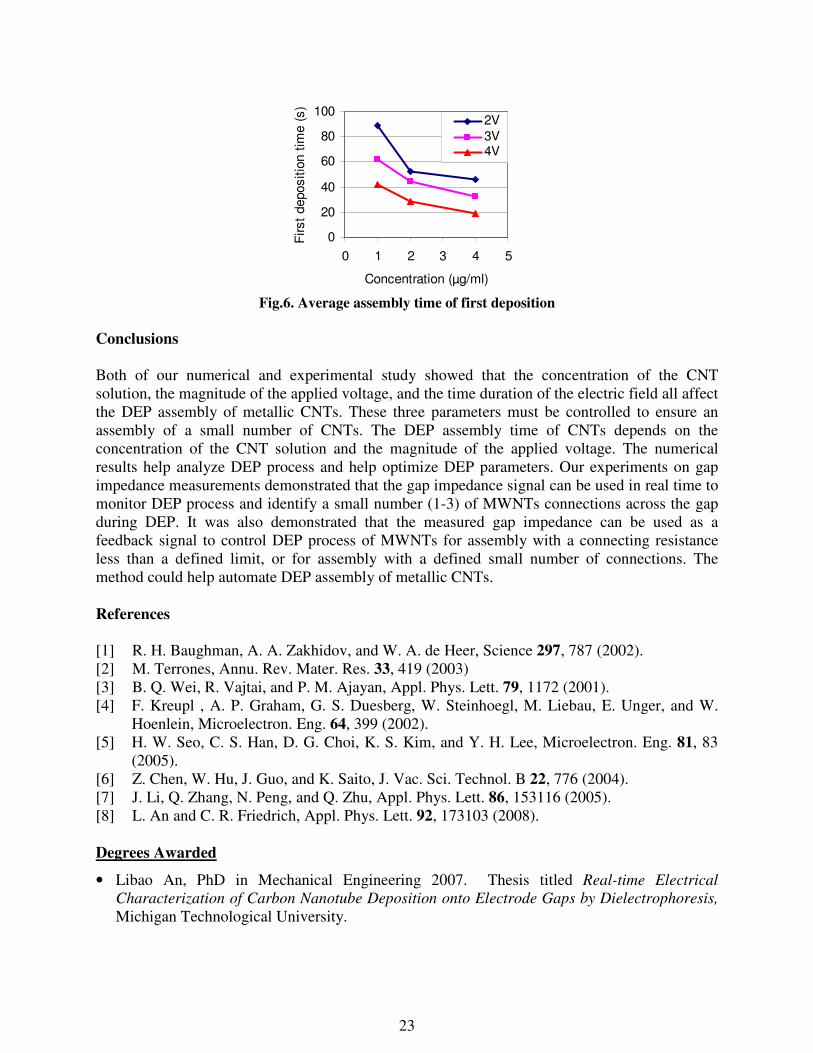
Effect of DEP process parameters was also experimentally studied and the experiments confirmed our simulation results. With our real-time gap impedance monitoring method [8], experiments were conducted to measure the assembly time of the first CNT connection. Fig.6 shows the average assembly time of the first connection across the gap under a variety of applied voltages and CNT concentrations.
0 20 40 6010
1
102
103
104
Assembly time (s)
Imp
ed
an
ce
(k
Ω)
(a) (c) -0.5 0 0.5-8
-4
0
4
8
Voltage (V)
Cu
rre
nt ( µ
A)
23
0
20
40
60
80
100
0 1 2 3 4 5
Concentration (µg/ml)
First
depositio
n t
ime (
s)
2V
3V4V
Fig.6. Average assembly time of first deposition
Conclusions
Both of our numerical and experimental study showed that the concentration of the CNT solution, the magnitude of the applied voltage, and the time duration of the electric field all affect the DEP assembly of metallic CNTs. These three parameters must be controlled to ensure an assembly of a small number of CNTs. The DEP assembly time of CNTs depends on the concentration of the CNT solution and the magnitude of the applied voltage. The numerical results help analyze DEP process and help optimize DEP parameters. Our experiments on gap impedance measurements demonstrated that the gap impedance signal can be used in real time to monitor DEP process and identify a small number (1-3) of MWNTs connections across the gap during DEP. It was also demonstrated that the measured gap impedance can be used as a feedback signal to control DEP process of MWNTs for assembly with a connecting resistance less than a defined limit, or for assembly with a defined small number of connections. The method could help automate DEP assembly of metallic CNTs. References [1] R. H. Baughman, A. A. Zakhidov, and W. A. de Heer, Science 297, 787 (2002). [2] M. Terrones, Annu. Rev. Mater. Res. 33, 419 (2003) [3] B. Q. Wei, R. Vajtai, and P. M. Ajayan, Appl. Phys. Lett. 79, 1172 (2001). [4] F. Kreupl , A. P. Graham, G. S. Duesberg, W. Steinhoegl, M. Liebau, E. Unger, and W.
Hoenlein, Microelectron. Eng. 64, 399 (2002). [5] H. W. Seo, C. S. Han, D. G. Choi, K. S. Kim, and Y. H. Lee, Microelectron. Eng. 81, 83
(2005). [6] Z. Chen, W. Hu, J. Guo, and K. Saito, J. Vac. Sci. Technol. B 22, 776 (2004). [7] J. Li, Q. Zhang, N. Peng, and Q. Zhu, Appl. Phys. Lett. 86, 153116 (2005). [8] L. An and C. R. Friedrich, Appl. Phys. Lett. 92, 173103 (2008). Degrees Awarded
• Libao An, PhD in Mechanical Engineering 2007. Thesis titled Real-time Electrical
Characterization of Carbon Nanotube Deposition onto Electrode Gaps by Dielectrophoresis, Michigan Technological University.

24
• Erin Burns, MS in Mechanical Engineering 2005. Thesis titled Micro-Electrode Fabrication
and Ion Implantation by Focused Ion Beam Machining, Michigan Technological University. • Sudip Thomas, MS in Mechanical Engineering 2005. Thesis titled Focused Ion Beam System
Characterization for Rates of Material Removal in Silicon, Michigan Technological University.
Refereed Journal Publications
• L. An and CR Friedrich, “Process parameters and their relationships for the dielectrophoretic assembly of carbon nanotubes”, Journal of Applied Physics Letters (105)6, 15 March 2009.
• L. An, DD Cheam, CR Friedrich, “Controlled dielectrophoretic assembly of multiwalled carbon nanotubes”, Journal of Physical Chemistry C (113) 37-39, 2009.
• L. An and CR Friedrich, "Real-time gap impedance monitoring of dielectrophoretic assembly of multiwalled carbon nanotubes," Virtual Journal of Nanoscale Science & Technology, May 12, 2008, http://www.vjnano.org.
• L. An and CR Friedrich,”Real-time gap impedance monitoring of dielectrophoretic assembly of multi-walled carbon nanotubes”, Applied Physics Letters (92) 173103, 2008.
Refereed Conference Publications
• Libao An and Craig R. Friedrich, “Real-time Electrical Characterization of Dielectrophoretic Assembly of Metallic Carbon Nanotubes”, in 2007 Materials Research Society Fall Meeting, Boston, MA, Nov. 26-30, 2007, Paper II17.3.L
• An and CR Friedrich, “2-D Simulation of Dielectrophoretic Assembly of Single Carbon Nanotubes Considering The Effect by the Electric Field”, Paper PP-23, Proceedings 25
th
Army Sciences Conference, Orlando, FL, November 2006.

25
Protein-Based Optical Nanosensors
Dr. Craig Friedrich, Professor, PI and Dr. Donald Lueking, Associate Professor Chris Anton (PhD 2008), Mark Griep (PhD 2008), Karl Walczak (PhD 2009), Eric Winder (PhD in progress) Department of Mechanical Engineering – Engineering Mechanics Department of Biological Sciences Photolithography Based Bacteriorhodopsin Patterning Technique
The photolithography based bacteriorhodopsin patterning technique (PBBPT) was developed to orient and deposit PM films onto a CMOS electronic substrate in such a way that the functionality of the PM is preserved. The deposition and patterning of photoactive PM films onto microelectronic devices will serve as the bottom layer in the proposed miniaturized detection system. This will create a light sensitive base platform that will be built upon by other researchers in this group to create the miniaturized toxin detection system. A schematic representation of the PBBPT process is shown in Figure 1.
Polished Silicon
Chrome
Gold
Photoresist
PM
Gold Coating
Electrodeposit PM film
Strip Resist/Film Liftoff
Cr/Au Coating on Photolithographically Patterned Substrate
Figure 1: Schematic representation of the PBBPT process

26
The PBBPT process starts by patterning a flat substrate through conventional photolithography. The photolithography process results in specific areas of the substrate being exposed while the remaining substrate is covered with a thin film (1.5 – 2.0 µm) of photoresist. If a non-conductive substrate is used, a 5 nm film of Cr followed by 15 nm of Au is sputter deposited over the entire substrate to provide a conductive surface for the PM deposition process. If a conductive substrate is used, this step is not necessary. Electrodeposition is used to orient and deposit PM patches onto the substrate. A liquid PM suspension is placed over the patterned area of the substrate. A second conductive plate (Au coated Si) is used to contact the top of the liquid suspension. A gap of 1.2 mm is maintained, and a voltage of 4.0 volts is applied between the substrate and the top plate. A second gold film can be sputter deposited onto the substrate after electrodeposition is performed. The purpose of this gold layer is to provide electrical contact with the top of the PM film while at the same time allowing for the majority of light to pass through the gold film and reach the PM below. Having electrical access to the top of the PM film allows for the film to be referenced to ground when integrated with microelectronic devices. To accomplish this, 6-8 nm of gold can be deposited onto the substrate prior to the photoresist liftoff step. The photoelectric functionality of the PM film is retained after a thin gold film sputter deposition. The final step in the PBBPT is to remove the photoresist. The substrate is placed in a sonicator that has been filled with acetone. Acetone has been found to remove the photoresist while leaving behind the dried PM films that are deposited onto the substrate. It has also been demonstrated that exposure to acetone does not negatively impact the photoelectric response of dried PM films. Sonication is used in conjunction with the acetone bath in order to facilitate photoresist removal and subsequent PM film patterning. What remains after the acetone sonication liftoff step is a series of patterned PM films on a single substrate. One important characteristic of any patterning process is the minimum feature size achievable using the process. To determine this characteristic for the PBBPT, a mask was designed using Cadence, and fabricated by Bandwidth Foundry. The chrome glass mask contained 18 rows of squares. Each row was seperated from the next by 400 µm. Nine square sizes were defined by the mask: 60 µm, 50 µm, 40 µm, 30 µm, 25 µm, 20 µm, 15 µm, 10 µm, and 5 µm. An ITO coated glass substrate was patterned using the mask described above. The PBBPT was used to pattern PM films onto a single substrate using this mask. The sample was imaged using a Hitachi S-4700 FE-SEM. A stage tilt of 45 degrees was used to gain some depth perspective, and was the reason the square patterns shown below appear distorted.
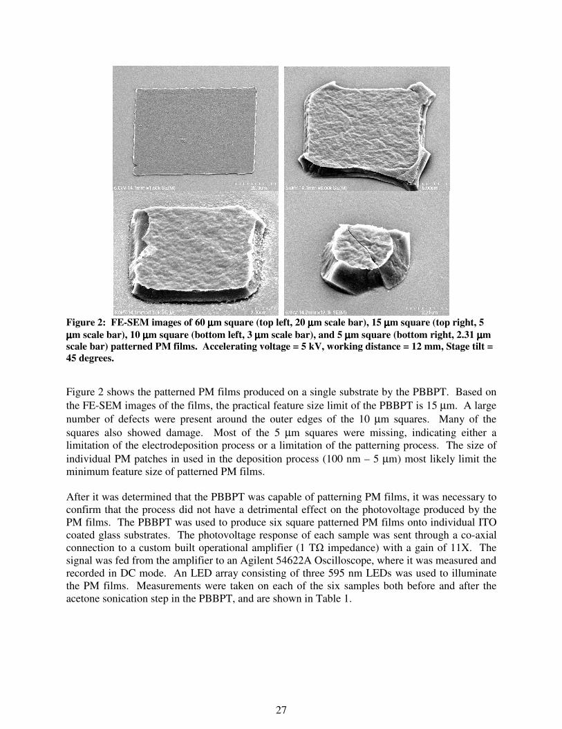
27
Figure 2: FE-SEM images of 60 µµµµm square (top left, 20 µµµµm scale bar), 15 µµµµm square (top right, 5
µµµµm scale bar), 10 µµµµm square (bottom left, 3 µµµµm scale bar), and 5 µµµµm square (bottom right, 2.31 µµµµm
scale bar) patterned PM films. Accelerating voltage = 5 kV, working distance = 12 mm, Stage tilt =
45 degrees.
Figure 2 shows the patterned PM films produced on a single substrate by the PBBPT. Based on the FE-SEM images of the films, the practical feature size limit of the PBBPT is 15 µm. A large number of defects were present around the outer edges of the 10 µm squares. Many of the squares also showed damage. Most of the 5 µm squares were missing, indicating either a limitation of the electrodeposition process or a limitation of the patterning process. The size of individual PM patches in used in the deposition process (100 nm – 5 µm) most likely limit the minimum feature size of patterned PM films. After it was determined that the PBBPT was capable of patterning PM films, it was necessary to confirm that the process did not have a detrimental effect on the photovoltage produced by the PM films. The PBBPT was used to produce six square patterned PM films onto individual ITO coated glass substrates. The photovoltage response of each sample was sent through a co-axial connection to a custom built operational amplifier (1 TΩ impedance) with a gain of 11X. The signal was fed from the amplifier to an Agilent 54622A Oscilloscope, where it was measured and recorded in DC mode. An LED array consisting of three 595 nm LEDs was used to illuminate the PM films. Measurements were taken on each of the six samples both before and after the acetone sonication step in the PBBPT, and are shown in Table 1.

28
Table 1: Acetone sonication time, pre-photoresist strip voltage, post-photoresist voltage and change
in voltage after the photoresist strip are shown. Voltages shown represent average peak to valley
voltages obtained from oscilloscope data.
Substrate
Square
Pattern Size
Acetone
Sonication
Time
Pre-Strip
Voltage
Post-Strip
Voltage
Change in Voltage
After Strip
4.0 mm 3 min 1.410 V 1.410 V 0 3.5 mm 8 min 0.940 V 1.875 V 0.935 3.0 mm 12 min 0.938 V 2.500 V 1.562 2.5 mm 12 min 0.781 V 1.719 V 0.938 2.0 mm 9 min 1.250 V 1.094 V -0.156 1.5 mm 9 min 0.625 V 0.625 V 0
As can be seen in Table 1, the acetone sonication bath did not negatively impact the photovoltage produced by the PM films. This result is significant, as it demonstrates that the PBBPT is capable of patterning PM films without negatively impacting the photoelectric properties of the film. The 2.5 mm, 3 mm, and 3.5 mm samples showed large increases in voltage due to light pulsing after the acetone sonication bath. This variation may be due to the acetone sonication bath removing un-oriented PM patches that may have been present on top of the samples. Because these three samples were not rinsed immediately after electrodeposition, unbound non-oriented PM patches most likely were dried on top of the oriented film. It is possible that the sonication in acetone removed some of these un-oriented films, which also increased the amount of light reaching the oriented film below. It is also possible that these variations were due to variations in the contact between the ITO top plate and the PM samples before and after the acetone sonication bath. However, these hypotheses were not investigated. Despite these variations in PM photovoltage output, this study does demonstrate that the photovoltage produced by PM films is not reduced or eliminated by the PBBPT. After it was determined that the PBBPT was capable of patterning PM films without eliminating the photoelectric response of the films, patterned PM films were integrated with MOSFET devices to create a light detection system. A six inch test wafer consisting of arrays of individually accessible PMOS and NMOS transistors was obtained from a major semiconductor manufacturer. Due to several characteristics of the MOSFET devices on the wafer (sensitivity to light, impedance mismatch with dried PM films), direct integration of patterned PM films onto the MOSFET substrate was unsuccessful. Instead, a remote integration test setup was devised. This setup connected a patterned PM film to the gate of an individual PMOS transistor using co-axial probes and a high impedance (1 TΩ, 2X gain) operational amplifier. The PM photovoltage signal was split after the operational amplifier and sent both to the gate of a single transistor, and to an oscilloscope. The oscilloscope measured the DC voltage produced by the PM film. The transistor response was measured using a Keithley 4200 semiconductor parametric analyzer (SPA). This experimental setup allowed the photovoltage produced by patterned PM films under illumination to activate an individual transistor, creating a light detection system. In order to characterize the sensitivity of the PM/transistor light detection system, a study was performed in which the light intensity was modulated and both the PM photovoltage and the

29
PMOS transistor response was measured. The results of this study are shown in Figure 3 and Figure 4 below.
PM Photovoltage vs. Light Intensity
0
0.05
0.1
0.15
0.2
0.25
0.3
0.35
0.4
0.45
0.0 0.2 0.4 0.6 0.8 1.0 1.2 1.4
Light Intensity @ 570 nm (mW/cm2)
PM
Ph
oto
vo
lta
ge
(V
)
Figure 3: Approximate maximum PM photovoltage versus LED light intensity.
Transistor Response vs. Light Intensity
0.0
0.2
0.4
0.6
0.8
1.0
1.2
1.4
1.6
1.8
2.0
0.0 0.2 0.4 0.6 0.8 1.0 1.2 1.4
Light Intensity @ 570 nm (mW/cm2)
Tra
ns
isto
r R
es
po
ns
e (
A)
Figure 4: Approximate maximum PMOS transistor drain current response versus LED light
intensity.

30
Figure 3 and Figure 4 show a consistent upward trend in both the PM photovoltage and the gate current of the transistor as the LED light intensity was increased. Figure 3 shows a roughly linear trend, with some reduction in the slope of the trend taking place at the last two data points. This slope reduction could be due to some portion of the bR molecules in the patterned PM film reaching saturation. Figure 4 shows a non-linear trend, with increased light intensities resulting in larger increases in transistor gate currents. This trend is expected due to the non-linear response characteristics of the PMOS transistor used in this experiment. This experiment has demonstrated the effectiveness of coupling PM films with MOSFET transistors. As the lighting conditions that the PM film is exposed to change, both the produced photovoltage and the transistor response change. This experiment has also shown that the patterned PM film was able to produce a photovoltage detectible by the PMOS transistor under very low light intensities. No detailed experiments investigating the impact of light intensity on the photovoltage produced by PM were found in the literature. This information will be necessary when a purpose-built system integrating PM films and microelectronics is designed.
Nano-Scale Interactions of Quantum Dots with the Optical Protein Bacteriorhodopsin The unique energy transfer interactions between the optical protein bacteriorhodopsin (bR) and
CdSe/ZnS quantum dots (QDs) provide a novel bio-nano electronics substrate with a variety of applications, including biosensing. To develop a functional bR/QD bio-nano electronics substrate, analysis of the nano-scale interactions of these nanomaterials was performed. The initial thrust behind integrating QDs with bR was to create a nano-scale light source for the activation of individual sites on a bR transistor array. Colloidal semiconductor QD’s with a diameter of ~3nm provide a photonic emission in the 570nm region, which is ideal for the activation of the bR photo cycle. Functional bR films, approximately 20 µm thick, were deposited on transparent indium tin oxide (ITO) substrates and the typical photo-electric response to a halogen light source is shown in Figure 1. To demonstrate the applicability of
Fig. 1. bR Photoelectric response to incadescent
light illumination (8mV/vertical division,
1sec/horizontal division).
Fig. 2. bR photoelectric response to 4Hz 575nm QD
illumination (2mv/ vertical division, 500ms/
horizontal division).

31
using QDs as the photon source, a colloidal suspension of 575nm QDs dropped in a well above the bR electrode. A 310nm LED-UV source was used to activate the QDs and the bR photo-electric response is shown in Figure 2. It can be observed that the bR photoresponse due to QD activation has less magnitude than halogen light source, which is directly related to the intensity of photons reaching the bR. With it being shown that the photonic output of QDs has the capability of activating the bR photoresponse, the ability to modulate the photovoltaic output of this bR/QD system was then evaluated. A process called fluorescence resonance energy transfer (FRET) is being explored to alter the QD photonic emission intensity based on its nano-scale proximity interactions with bR. A primary factor for a FRET relationship to exist is a strong overlap in the donor (QD) excitation and acceptor (bR) absorbance peaks. As shown in Figure 3, a hybrid bR/QD system can be engineered to maximize this spectral overlap to enhance FRET efficiency. Using known equations, a bR/QD FRET relationship can be modeled to demonstrate where maximal energy transfer will occur versus bR/QD separation distance, as shown in Figure 4. The distance at which 50% of the QD’s energy is transferred non-photonically to the bR is known as the Forster radius (Ro), which was theoretically calculated to be 6.2nm for a 565nm QD/bR system and 6.12nm for a 600nm QD/bR system. Therefore with a separation distance of 6.2nm between the 565nm emission QD and a bR molecule, half of the QD energy will be transferred to the bR molecule non-photonically. The theoretical calculations also suggest that increasing the peak QD emission by 35nm only decreases Ro by 0.08 nm, thus the use of QDs at 570nm emission is not critical. It can be noted from Figure 4 that the degree of FRET efficiency can vary greatly over a small change (< 1nm) in separation distance, particularly around the Forster radius (E = 50%).
Fig. 3. Spectral comparison of 570 nm QD
and bR. The high degree of overlap between
bR absorbance and QD emission is one
criteria for forming a FRET coupling system.
Fig. 4. Theoretical FRET efficiency (E) vs. bR/QD
separation distance (R). At the Forster radius, a
small change in bR/QD separation distance results
in a sharp alteration in bR/QD energy transfer.
0.00%
20.00%
40.00%
60.00%
80.00%
100.00%
0 5 10 15
R (nm)
E (
%)

32
To demonstrate the presence of a bR/QD FRET coupling relationship in an aqueous system, a biotin/streptavidin linkage system was implemented to ensure a nano-scale separation distance between the bR and QD molecules. As shown in Figure 5, the integration of bR and QDs results in substantial quenching of the QD photonic emission of around 32.5% at its maximal point, which is likely due to both FRET and other absorptive processes. The FRET relationship shown in Figure 5 was performed with bR in the larger purple membrane fragment form which has the potential to create steric hindrances and have macromolecule-type folding that could inhibit QD integration with a large majority of the bR molecules. These phenomena could partly explain why it took upwards of 81 bR molecules per QD to achieve maximal FRET quenching. To overcome these obstacles bR was created in its monomer form through the application of detergent techniques. Again using a biotin/streptavidin linkage scheme, the FRET relationship of a bR monomer/QD system was examined and shown in Figure 6. It can be seen that a larger FRET maxima is achieved at even smaller bR:QD ratios than observed when using bR in its purple membrane fragment form. A maximal FRET efficiency of 49.31% was observed at a bR:QD ratio of 2:1.
Fig. 5. Aqueous bR/QD coupling
demonstrating a 32.5% reduction in QD
emission. Proximity achieved with
biotin/streptavidin linking system .
Fig. 6. Aqueous bR/QD coupling with
biotinylated bR monomers. Monomeric bR
displays more efficient coupling than the
membrane fragment form.
0
100000
200000
300000
400000
500000
550 575 600 625 650
Wavelength (nm)
QD
Flu
ore
sc
en
ce
(c
ps
)
QD only
1 QD : 0.27 bR
1 QD : 2.7 bR
1 QD : 28 bR
1 QD : 56 bR
1 QD : 84 bR
0
0.1
0.2
0.3
0.4
0.5
0.6
0.7
0.8
0.9
1
500 525 550 575 600 625 650 675 700
Wavelength (nm)
No
rma
liz
ed
Em
iss
ion
(a
.u.) Normalized Control
2:1 bR:QD
15:1 bR:QD
25:1 bR:QD
100:1 bR:QD

33
To further study the bR/QD interactions in a dried state, particularly the potential FRET coupling relationship, nano-scale assembly techniques must be utilized as the FRET relationship is only achieved with sub-10nm bR/QD separation distances. In order to achieve close proximity along with a high degree of film orientation we have used Ionic Self Assembled Monolayers (I-SAMs) techniques which utilize the inherent charge on the material to build alternate positively/negatively charged monolayers through electrostatic adsorption. The results demonstrate that bR retains its functionality in these films, thus it is feasible to utilize the I-SAM method as a means of creating multi-layer bR/QD thim films for bio-nanoelectronic applications. To accomplish this, a polydimethyldiallyammonium chloride (PDAC) based I-SAM technique was utilized to create bilayer, trilayer and mixed-multilayer systems of alternating monolayers of bR (-), PDAC (+) and QD’s (-) on a conductive ITO substrate. The construction of multilayer
systems was directly monitored by measuring the unique A570nm absorbance of bR, as well as the 570nm QD fluorescence emission. As shown in Figure’s 7 and 8, a linear monolayer deposition was observed over multiple layers for bR and QD systems, respectively. Atomic force microscopy studies confirmed single monolayer deposition of purple membrane fragements with a film thickness of 5.5nm (data not shown). With the results confirming that bR/PDAC and QD/PDAC bilayer I-SAM films could be separately constructed with the current method, emphasis was placed on the integration of bR and QDs into a multilayered I-SAM film. The layering structure of the first layer of this conjugate system, for example, is: ITO-PDAC-bR-PDAC-QD, with the pattern repeating (excluding the ITO) for consecutive layers. The bR/PDAC/QD conjugate film growth can be tracked by monitoring the increasing QD emission peak (λ=570nm), as shown in Figure 9. The inset in Figure 9 shows the quenching effect of the additional bR layer on top of the full trilayer, which results to an additional 20% reduction, on average, to the QD emission. The QD
0
0.01
0.02
0.03
0.04
0.05
0.06
0.07
500 520 540 560 580 600 620 640
Wavelength (nm)
Ab
so
rba
nc
e (
a.u
.)
Blank
2 bilayers
4 bilayers
6 bilayers
8 bilayers
10 bilayers
12 bilayers
0
0.02
0.04
0.06
0.08
0 4 8 12
Bilayer (#)
57
0n
m A
bs
. (a
.u.)
Fig. 7. bR absorbance spectra for select
bR/PDAC bilayers as it is assembled. Bilayers
constructed on negatively charded ITO with
PDAC (+) and bR (-) being alternately deposited.
Inset tracks 570nm absorbance of the bR retinal
during consecutive bilayer depositions.
0
20000
40000
60000
80000
100000
120000
140000
160000
180000
200000
520 540 560 580 600 620
Wavelength (nm)
Em
iss
ion
(c
ps
)
1 bilayer
2 bilayers
3 bilayers
4 bilayers
5 bilayers
6 bilayers
7 bilayers
8 bilayers
0
50000
100000
150000
200000
0 2 4 6 8 10
Bilayer (#)
57
0n
m E
mis
sio
n (
cp
s)
Fig. 8. QD fluorescence emission for each
QD/PDAC I-SAM bilayer as it is assembled.
Inset displays linear trend in QD monolayer
assembly.

34
quenching effects can be attributed to a combination of bR absorption in the QD emission spectra along with potential fluorescence resonance energy transfer (FRET) between the QDs and bR retinal. Evaluation of QD fluorescence emission in the multilayer system strongly suggests that FRET coupling is occurring and, since the I-SAM technique provide a means to control the bR/QD separation distance on the nanometer scale, this technique may prove highly valuable for optimizing the distance dependent energy transfer effects for maximum sensitivity to target molecule binding by a biosensor. The impact of bR/QD FRET coupling is further exemplified in Figure 10, which compares the quenching of a single QD monolayer versus number of bR layers in FRET coupling range. Results suggest that the QD’s strongly FRET couple with the first bR layer it is in direct contact with, culminating in a 37% FRET efficiency. Further bR layers only reduce QD emission by <10% which is likely due to primarily absorptive effects. The photovoltaic response of bilayers of bR/PDAC was observed over a range of 1 to 12 bR monolayers and the ability to efficiently create an electrically active multilayered substrate composed of bR and QDs has been demonstrated for the first time. To measure the electrical activity of the PM I-SAM films and electrochemical cell setup was created; using 0.5M KCL was used as the electrolyte. The output in the DC-coupled electrochemical cell measurement setup produced a steady-state voltage output, in contrast to a transient signal in the traditional AC-coupled measurement setup. The ability of this substrate to alter its photovoltaic output based on photonic intensity was demonstrated. With a ~50% reduction in incident light intensity, the magnitude of the bR photoelectric response immediately reduces to a lower steady-state voltage output. Importantly, efficient FRET coupling in the bR/QD system that result in altered QD emission intensity may serve as a modulation focus for the alteration of bR electrical output. Since monolayer bR/QD films created with the I-SAM technique provide a means to control the bR/QD separation distance on the nanometer scale, this technique may prove highly valuable for optimizing the distance dependent energy transfer effects for maximum sensitivity
0
20000
40000
60000
80000
100000
120000
520 540 560 580 600 620
Wavelength (nm)
Em
iss
ion
(c
ps
) 1 trilayer
1.5 trilayers
2 trilayers
2.5 trilayers
3 trilayers
3.5 trilayers
4 trilayers
4.5 trilayers
5 trilayers
5.5 trilayers
6 trilayers
Blank
0
20000
40000
60000
80000
100000
120000
0 1 2 3 4 5 6 7
Tri-layer (#)
57
0n
m E
mis
sio
n (
cp
s)
Fig. 9. QD fluorescence emission for each
bR/PDAC//QD I-SAM trilayer as it is
assembled. The half layers signify an additional
bR monolayer on top of the existing trilayers.
Inset displays effects of bR on QD emission
during trilayer assembly.
Fig. 10. Quenching of QD emission in bR/QD
I-SAM film, with a 37% emission reduction
from the first bR layer and <10% reduction
for each subsequent bR layer.

35
to target molecule binding. In any event, the ability to engineer nanoscale bR/QD multilayered films utilizing the I-SAM technique will undoubtedly prompt further research on the nanoelectronic properties of the bR/QD system.
Integration of the Bacteriorhodopsin and Single Electron Transistors
Introduction
The current hazardous sensors are too bulky, complex, and costly. Technological improvement in sensing technologies to detect chemical and biological agents is needed. The thrusts behind this research are to develop hazardous sensor technologies which can be utilized in the field. The technology developed would help create a sensor which is; lightweight, disposable, wireless, deployable by hand, and configurable. This paper will present initial results on the development technology for a sensing platform which incorporates a nanoelectronic device with a bionanomaterial. Bacteriorhodopsin is a light activated proton pump contained in the cytoplasmic member of purple membrane of the bacterium Halobacterium salinarum. Bacteriorhodopsin generates a voltage and current in response to visible light. Bacteriorhodopsin is a robust protein which can function in both wet and dry states and can withstand extreme environmental conditions [1]. A single electron transistor (SET) is a nano-scale transistor that exploits the quantum mechanical properties of electrons to switch on and off. SETs have tremendous potential in practical applications due to their size, ultra low power requirements, and electrometer-like sensitivity. SETs are extremely sensitive to minute changes in gate voltages. Since small variations in electrical gate potential changes the current versus voltage (IV) and current versus time (I-T) curves of the SET. Bacteriorhodopsin immobilized on the gate would generate an electrical potential in response to light, which could possibly modulate the electrical functionality of the SET. Methods and Results
The integration of the photosensitive bionanomaterial bacteriorhodopsin with single electron transistors is a hybrid device, composed of both biological and nonbiological components. This represents the first report of a bionanomaterial being integrated with a SET. The SETs were fabricated by a process described by [2] with couple of modifications. First, photolithography was used to decrease the time to FIB devices by patterning the general architecture of the devices as shown in Fig. 1. Second, a liftoff process was used to remove the Al2O3 from the device pads. Third, the gate size was increased from 100 µm x 100 µm. Each of the SETs contains three electrodes Drain\Source\Gate (Fig.1) which are separated by FIB etching as shown in Fig. 2. Enlarging the gate increases the amount of bR integrated with the SET as shown in Fig.1. Since the voltage generated by bR from the proton pumping/shifting is vectorial. The more oriented bR deposited on the gate the greater the voltage generated. Generating a large voltage on gate will increase the possibility of modulating the SET with bR.

36
Prior to bR integration with SETs baseline characteristic were established by measuring the current versus voltage (IV) curves with and without light illuminating the gate as shown in Fig. 3. The light source was composed of three amber LEDs. Baseline characterization indicated that the functional characteristics of the SETs were not influenced by light.
Gate
Source Drain
Quantum
islands
Pad for bR
256um
150um
200-10nm
Fig. 1. Architecture for bR SET.
A. B.
Fig. 2. FESEM images of gap of SET.

37
-1.00
-0.50
0.00
0.50
1.00
-1.50 -0.50 0.50 1.50
Voltage (V)
Cur
rent
(nA
)
With light flashing Without light
With constant light
Fig. 3. SET I-V curves with light flashing, constant, and without.
Bacteriorhodopsin was then electrophoretically deposited on the gate of the SETs. The bR SETs were then characterized with and without light illuminating the gate and this data was compared to baseline measurements. The voltage and current generated by illuminating bR on the gate of the SET caused a change in the current flowing between the source and drain of the device as shown in Fig. 4. Too ensure that the change in current across the source and drain was due to the bR and not some artifact of the LED circuit, multiple tests were conducted. First, the light was blocked without moving the LEDs. Blocking the LEDs eliminated the current change across the source and drain as the LEDs were flashed. Then, the optical power of the LEDs were varied since the voltage potential of bR is dependent on the optical power of the illumination source, the larger the optical power the larger the voltage generate by bR. As shown in Fig. 4, changing the optical power of the LEDs caused a change in the amount of current flowing between the source and drain. These graphs indicate increasing the optical power of the LEDs increases the current flowing between the source and drain. Next to establish an understanding of the controllability of the SET the bias voltage on the source terminal was varied to attempt to control the current flowing between the source and drain. The bias voltages on the source terminal were determined from the characteristic IV curve shown in Fig. 5. By changing the bias voltage on the source terminal, the current flowing across the source drain gap could be controlled: off, on, and amplified as shown in Fig. 5. As shown in Fig. 4, with a bias voltage of -20 V the current from the source to the drain is about 2 picoamps and with a bias voltage of 0V no current is flowing between the source and drain. In conclusion this work has shown it is possible: 1) to integrate a nanomaterial and nanotransistor, 2) to modulate the output of the SET with bR, and 3) control the sensitivity of the SET by change the bias voltage. With this initial research into the integration of the bR with a SET it is hoped that this technology developed will eventually lead to creation of an inexpensive, super sensitive toxin sensor. The sensor developed could then be used to save the lives of soldiers and civilians.

38
-2.50
-1.50
-0.50
0.50
1.50
2.50
100.00 150.00
Time (sec)
Cur
rent
(pi
coA
mps
)
Bias 0V LED 1.1 (Amps)
Bias 0V LED 1.37 (Amps)
-20.00-18.00-16.00-14.00-12.00-10.00
-8.00-6.00
105.00 135.00 165.00 195.00
Time (Sec)
Cur
rent
(pi
coA
mps
)
Bias -20V LED 1.1 (Amps)
Bias -20V LED 1.37 (Amps)
ON OFF
Fig. 4. Current versus Time (IT) curve A) -20 V and B) 0V.
-100.00
-50.00
0.00
50.00
100.00
-25 -15 -5 5 15 25
Voltage (V)
Cur
rent
(pi
coA
mps
)
0
0.5
1
1.5
2
2.5
3
-25 -15 -5 5 15 25
Bais voltage (V)
Cur
rent
(Pi
coA
mps
)
LED Power 1.1Amps LED Power 1.37 Amps
Fig. 5. A) bR SET IV curve of device under test. B) Current across the source and drain at different
bias voltages.

39
References
[1] N. Vsevolodov, Biomolecular electronics an introduction via photosensitive proteins
1998. [2] P. S. K. Karre, P. L. Bergstrom, G. Mallick, and S. P. Karna, "Room temperature operational single electron transistor fabricated by focused ion beam deposition " Journal of
Applied Physics, vol. 102, pp. 1-4, 2007. Fused Protein Nanosensor Material The specificity and sensitivity of the protein based nanosensor will rely upon a sensor protein-bacteriorhodopsin fused protein. Having established a voltage output from FRET coupling this fused protein with a quantum dot, or by direct quantum dot illumination, the binding energy resulting from the interaction of a target molecule with the sensor protein is proposed to be of sufficient intensity to perturb the produced voltage and register the presence of the target molecule. To date, these studies have focused upon identifying and isolating the gene for bR and constructing an expression vector that will allow the production of the bR protein fused to an experimental sensor protein. In this regard, primers were designed using the published DNA sequence of bR and these primers were then utilized to identify and amplify the bR gene from whole cells of Halobacterium salinarium using a colony level PCR technique. Following purification, the resulting PCR products were evaluated by agarose (0.7%) gel electrophoresis (Figure 1) and the prominent (0.84kb) band putatively identified as the bR gene fragment was recovered from the gel and cloned into the AT vector pGEM-T.
Following introduction of this vector into cells of E. coli JM109 by electroporation, transformants containing the plasmid vector with the cloned bR insert were identified, the plasmid purified and the presence of the bR gene sequence confirmed by di-deoxy BigDye termination DNA sequencing (Sanger method). Importantly, the isolated and cloned 0.840 kb fragment was shown to contain the complete bR gene sequence which comprised 789 of the 840 nucleotides. Primer-adaptors were subsequently designed to modify the ends of the isolated bR gene thereby facilitating its directional insertion into the plasmid pMal-c4e expression vector. This commercial vector contains the gene sequence for the well-characterized maltose binding protein and is designed to allow the production of the maltose binding protein directly fused to other proteins in an E. coli experimental system. Our objective is to produce the maltose binding protein fused to bR and subsequently use the disaccharide maltose as the first target molecule for the development of the proof-of-concept protein based nanosensor.

40
Figure 1: Agarose gel 0.7% of PCR products from reaction utilizing bacteriorhodopsin primers.
From left to right, lane 1, Qiagen GelPilot 1kb Ladder with brightest band signifying 1kb; lanes 2-
5, PCR products with varying reaction buffers; lane 6, empty; lane 7, New England Biolabs (NEB)
100bp Ladder with the brightest band at 1kb; lane 8, NEB 1kb Ladder with brightest band at 3kb.
The first modification was to convert the isolated 840 base pair DNA duplex strand composed of the bR gene with one extra upstream base and fifty extra downstream bases, denoted as bR.840.1.50, to include unique restriction/cut sites upstream and downstream of the gene for insertion into a cloning vector. The upstream DNA was modified by the use of a Primer-Adaptor and PCR to add 8 upstream bases, which includes the unique restriction site, GAATTC, for the endonuclease EcoRI. This modification was confirmed by DNA sequencing combined with BLASTn analysis, yielding a novel DNA strand denoted as EcobR. This novel construct is shown with the original isolation in Figure 2, below.
Figure 2: A, shows the isolated DNA from Halobacterium salinarum, bR 840.1.50, with the core 789
nucleotides shown in purple and the extra up/down-stream bases given in red; B, shows the novel
EcobR 848.9.50, with the new upstream bases
The downstream DNA of EcobR (848.9.50) was then modified by first using the restriction enzyme AlwNI that recognizes the sequence CAGNNNCTG with N being any of the four possible DNA nucleotides, as its cut site, to remove fifty-three bases from the downstream side. These fifty-three removed bases included three bases of the bR gene giving a resultant fragment

41
of size of 795.9.-3. Using the EcoRI forward primer-adaptor(above) with a new reverse primer-adaptor of twenty-one bases including the removed bR bases and the sequences GGATCC and CTGCAG that are the unique restriction sites for the restriction endonucleases BamHI and PstI, respectively, the 795.9.-3 construct was amplified. The resulting construct denoted as EcobRBamPst with sizing 816.9.18 was confirmed by DNA sequencing combined with BLASTn analysis. The results of this digestion and resultant primer-adaptor PCR is shown below in Figure 3.
Figure 3: A, the result of the removal of the downstream bases by AlwNI digestion; B, the resultant
construct EcobRBamPst after primer-adaptor PCR with the additional downstream bases given in
green.
This novel EcobRBamPst construct was then double digested with EcoRI and BamHI in sequential reactions while concurrently, the New England Biolabs commercial vector pMal-c4e was also double digested (DD) with the same EcoRI and BamHI restriction enzymes. Both enzymes leave sticky ends post-digestion that facilitate annealing and subsequent ligation. This reaction allows the directional insertion of the construct into the plasmid vector to form a contiguous, circular dsDNA vector comprised of the pMal-c4e vector and the bR gene. Initial attempts to express the protein from the pMAL vector in cells of Escherichia coli strains JM109 and DH5-α were unsuccessful. Protein expression in the pMAL vector is driven by a Ptac promoter, which should result in a prolific production of the fused protein. However, numerous induction studies employing SDS-PAGE to qualitatively monitor whole cell protein production failed to indicate the production of a new fused protein product. Alternately, the fused gene construct present in the pMAL vector was completely recovered by PCR and subsequently cloned into the expression vector pET-200 (Invitrogen). This vector is designed to work with an Escherichia coli BL21(DE3) host strain to drive the expression of cloned genes from a strong T7 promoter. Although the fidelity and reading frame compatibility of this new plasmid construct were confirmed by DNA sequencing, attempts to express a putative fused protein were also unsuccessful. However, the production of a low molecular weight protein was routinely observed, which indicated that an additional transcription initiation start site(s) might be present and competing with the true start site for transcription. In fact, a re-evaluation of the DNA sequence constituting the fused gene construct revealed three, previously overlooked, initiation start sites that could account for the production of the low molecular weight protein product. Utilizing novel primers for site-directed mutagenesis to remove, or silently mutate, the alternate start sites to produce alternate codons which code for the same amino acid, but no longer constitute an initiation start site allowed transcription of the fused gene from the proper position. Initial induction and expression studies are shown in the attached figure of an SDS gel (Figure 4). Sequencing shows that transformant 1 had no mutations from the wild-type bR, while

42
transformant 3 had at least 2 of the 3 site-directed mutations in its sequence. It is also transformant 3 that shows a large induction band signifying a protein with an apparent molecular weight of approximately 55kDa. Purification, identification and scale-up processes of the protein produced by transformant 3 are currently underway. Preliminary studies have shown that the fused protein is produced as an inclusion body and this feature may present problems for the purification and renaturation of the protein. The goal is to purify and renature (add retinal) the fused protein and to determine if this modified bR retains it characteristic properties and electrical activity.
Figure 4: SDS-PAGE image of induced E. coli transformants. From left to right the lanes are:
Mark12 Standard Ladder, transformant 1 not induced, transformant 1 induced at 3 hours,
transformant 1 induced at 9 hours, Transformant 2 not induced, transformant 2 induced at 3
hours, transformant 2 induced at 9 hours, transformant 3 not induced, transformant 3 induced at 3
hours, transformant 3 induced at 9 hours.
Degrees Awarded / In Progress
• Christopher Anton, PhD in Mechanical Engineering 2008. Thesis titled Photolithography
Based Patterning of Bacteriorhodopsin Films, Michigan Technological University. • Mark Griep, PhD in Mechanical Engineering 2008. Thesis titled Integration of quantum Dots
with Bacteriorhodopsin, Michigan Technological University. • Karl Walczak, PhD in Mechanical Engineering 2009. Thesis titled Immobilizing Purple
Membrane on a Single Electron Transistor, Michigan Technological University. • Eric Winder, PhD in Biological Sciences (in progress). Thesis titled Chemical and Biological
Sensing Utilizing Fused Bacteriorhodopsin Protein Hybrid, Michigan Technological University.

43
Refereed Journal Publications
• Griep,M, Winder,E, Lueking,D, Friedrich,C, Mallick,G, and Karna,S, “Optical Protein Modulation via Quantum Dot Coupling and Use of A Hybrid Sensor Protein”, Journal for
Nanoscience and Nanotechnology, in press. • Anton,C, Walczak,K, Lueking,D, and Friedrich,C, “Integration of Optical Protein With
Electronics For Bio-Nanosensors”, Journal for Nanoscience and Nanotechnology, in press. • Griep,M, Walczak,K, Winder,E, Lueking,D, Friedrich,C, “Quantum Dot Enhancement of
Bacteriorhodopsin-Based Electrodes”, for submission Journal of Biosensors and
Bioelectronics, 2009.
Refereed Conference Publications
• E. Winder, D. Lueking, C. Friedrich, “Chemical and Biological Sensing Utilizing Fused Bacteriorhodopsin Protein Hybrids”, 26
th Army Science Conference, Orlando, FL, December
2008. • K. Walczak, M. Acharya, D. Lueking, P. Bergstrom, C, Friedrich, “Integration of the
Bionanomaterial Bacteriorhodopsin and Single Electron Transistors”, 26th
Army Science
Conference, Orlando, FL, December 2008. • Karl A. Walczak, Daw Don Cheam, Don Lueking, Paul L. Bergstrom, Craig Friedrich,
“Electronic Characteristics of Bacteriorhodopsin”, IEEE Nano 2008, 8th International Conference on Nanotechnology, Arlington, TX, August 2008.
• M. Griep, G. Mallick, D. Lueking, C. Friedrich, S. Karna, “Integration of Optical Protein and Quantum Dot Films for Biosensing”, IEEE Nano 2008, 8
th International Conference on
Nanotechnology, Arlington, TX, August 2008. • C. Anton, K. Walczak, D. Lueking, C. Friedrich, “Integration of Optical Protein With
Electronics for Bio-Nanosensors”, 1st International Conference from Nanoparticles and
Nanomaterials to Nanodevices and Nanosystems, Halkidiki, Greece, June 2008. • M. Griep, E. Winder, D. Lueking, C. Friedrich, G. Mallick, S. Karna, “Optical Protein
Modulation via Quantum Dot Coupling and Use of a Hybrid Sensor Protein”, 1stInternational
Conference from Nanoparticles and Nanomaterials to Nanodevices and Nanosystems, Halkidiki, Greece, June 2008.
• Anton, C., Griep, M., Walczak, K., Winder, E., Lueking, D., Friedrich, CR, “Integration of Optical Protein with Nanomaterials and Electronics for Bio-Nanosensors”, Proceedings Indo-
US Workshop on Science and Technology at the Nano-Bio Interface, Bhubaneswar, India, February 2008.
• Griep, M, Walczak, K, Winder, E, Lueking, D, Friedrich, CR, “An integrated bionanosensing method for airborne toxin detection,” Proc. SPIE, Vol. 6646 (2007), 66460F.
• Walczak,K, Lueking,D, Friedrich,C, “Nanoengineering Applications with the Biophotonic Nanomaterial Bacteriorhodopsin”, Michigan Alliance in Nano Science and Engineering
Symposium, Oakland University, May 2007. • Griep, M, Lueking, D, and Friedrich, C, “Quantum Dots as an Onboard Light-Source for
Activation of Bacteriorhodopsin Based Nanosensors”, Paper MO-23, Proceedings 25th
Army
Sciences Conference, Orlando, FL, November 2006.

44
• Anton, C, Lueking, D, and Friedrich, C, “Effects of Focused Ion Beam Machining on Oriented Bacteriorhodopsin Optical Protein Films”, Paper MP-15, Proceedings 25
th Army
Sciences Conference, Orlando, FL, November 2006. • Friedrich, C, “Protein Nanosensors for Multi-Scale Technologies”, Proceedings International
Symposium on Frontiers in Nanoscale Science, Technology, and Education, Cochin, India, August 2006.
Patent Disclosures
• Patent Disclosure, C Friedrich, M Griep, D Lueking, , C Friedrich, M Griep, D Lueking, “Method for Modulating Electrical Activity of Opto-electronic Protein by Proximity of Quantum Dots”, #0638.00.
• Non-Provisional Application, US Application No. 12/325.718, C Friedrich, M Griep, D Lueking, Patent Disclosure, C Friedrich, M Griep, D Lueking, “Bacteriorhodopsin Based Sensors”, Dec. 2008.
Student Awards
• PhD candidate Mr. Mark Griep was awarded a NSF Graduate Student Fellowship for a period of three years, by which a portion of this research was supported. He was also awarded a Fulbright Fellowship, after which he will complete his portion of this research.

45
Planar Magnetic Photonic Crystals for Integrated Photonic Devices
Dr. Miguel Levy, Associate Professor, Co-PI and Dr. A.A. Jalali, Post-Doctoral Fellow Xiaoyue Huang (PhD 2007) Ziyou Zhou (PhD in progress 2008), Zhuoyuan Wu (PhD in progress 2010) Department of Physics Department of Materials Science and Engineering During the course of this project we conducted a systematic program for the development of efficient on-chip magnetophotonic crystal structures by focused ion beam patterning. This program was highly successful and enabled a number of other studies and projects that were based on magnetophotonic crystal performance. The work that was carried out studied and developed techniques for deep-groove and efficient Bragg structures in magnetic garnet films and demonstrated the formation of bandgaps and large magneto-optic polarization response. Photonic crystals showing high polarization sensitivity to applied magnetic fields for sensor applications were developed and tested. The following studies were conducted and completed during this project: Groove-depth performance, characterization and optimization of planar one-dimensional magnetophotonic crystals, grating uniformity and period variability studies, magnetic field strength dependence of the transmittance and polarization response, temperature-dependence of the transmittance and polarization response, a comparative study of the response in magnetophotonic crystals with and without resonant cavities showing band edge effects in the latter. Towards the last phase of the project we initiated the study of group velocity in magnetophotonic crystals and the effect of asymmetries in the patterned structures. Theoretical and simulation studies were conducted, the latter using a commercial simulation package for waveguide photonic crystals. These studies showed the presence of asymmetries in the band structures between forward and backward propagation directions in on-chip photonic crystals with tilted grooves- and hole-arrays. Experimental work was performed to develop the technology for fabricating these asymmetric structures. This work succeeded in the fabrication of such structures by focused ion beam patterning. Transmittance tests were carried out showing differences in response for different waveguide mode launch conditions. This work has laid a strong basis to continue the study of asymmetric photonic crystal structures in magnetic systems after the expiration of this contract. During this project the conditions for the fabrication of 400nm- to 1000-nm deep grooves photonic crystals on magnetic garnet films were established. A photonic device simulation tool was purchased and applied to the design of the devices under fabrication. The study of conditions for the focused-ion-beam (FIB) fabrication of deep-groove magnetic photonic crystals in Bi-substituted yttrium iron garnet (Bi-YIG) film waveguides was successfully pursued. Figures 1 shows SEM and AFM micrograph images of magnetophotonic crystals fabricated on chip, the latter on a ridge waveguide.

46
Transmittance and polarization rotation studies on these structures were carried out for ridge waveguides fabricated on Bi-YIG films by Ar-ion (CAIBE) and Ga-ion (FIB) milling. Questions addressed were: (1) the determination of grating groove depth versus ion beam current and ion-milling repetition number, and (2) the formation of photonic crystal grating structures directly on pre-fabricated waveguide ridges. The ability to fabricate photonic crystal patterns directly on pre-fabricated Bi-YIG ridge waveguides was demonstrated. This was a particularly important step as it showed the viability of magnetophotonic crystals on waveguide structures. Figures 2 and 3 show typical transmittance and polarization response obtained in magnetophotonic crystals fabricated in our laboratory by this technique. A particularly important feature is the existence of photonic stopbands from optical bandgaps in the dispersion. Various properties of the photonic crystals were studied in the course of this project. These included grating period variability, waveguide loss, and magnetic field and temperature dependence of the Faraday rotation response in these crystals. Grating period variability was studied by field emission SEM. Small variations were found but these were shown not to contribute significantly to spurious effects in the performance of the photonic crystal. Our
Fig. 1. Scanning-electron micrograph of deep-groove photonic crystal pattern fabricated
by focused-ion-beam on magnetic garnet films (left). Right: AFM image of magnetic
photonic crystal ridge waveguide fabricated by focused ion beam milling on a magnetic
garnet. A seven-quarter wavelength-long resonant cavity is visible in the middle.
Figure 2. Transmitted power and polarization
response of the fundamental mode resonance.
A 7°°°° polarization rotation is observed in spite
of the 0.005 fundamental-mode birefringence
for the sample.

47
studies demonstrated that variations of less than 1 nm in 200µm-long gratings were possible by focused-ion-beam patterning. Magnetic field dependence in the optical response demonstrated that saturation of the magnetization was achievable with fields near 100 Oe in these films.
A study of environmental temperature effects on waveguide magnetic photonic crystal performance was performed as part of this project. A testing platform for end-fire coupling was designed and built for this purpose. Waveguide photonic crystal samples were fabricated and transmittance and Faraday rotation measurements performed. This study showed that temperature fluctuations are not a significant factor in transmittance performance at room temperature but noticeable changes can be seen at high temperatures. An analysis of optical speed effects in the band gap and near the band edge in these photonic crystals was also carried out.
Extensive use was made of the interplay between experimental data and theoretical analysis. Optical speed control is of interest because of potential applications to phased array radar technology and rotation sensing. A study of the group and the energy velocities and analysis of the superluminal effect for one-dimensional magnetic photonic crystals in the band gap and near the band edges was performed. This study yielded a relation between phase shifts in the normal modes and a group velocity, based on the total accumulated phase, as the light propagates in the structure. It was shown that optical slow down by a factor of 4 near the band edges was achievable in these structures.
One-dimensional magnetic photonic crystals without resonant cavities were developed and a study of the transmittance and Faraday rotation response thereof was carried out. Waveguide magnetophotonic crystals were fabricated on (Bi,Lu)(2.8 ± 0.1)Fe(4.6 ± 0.2)O(12.4 ± 0.3) films on (111) gadolinium gallium garnet (GGG) substrates or this purpose. Fundamental to first-order mode coupling were analyzed and compared. A resonant Faraday response near the band edge was found but no resonance at the center of the stop band. Typical transmittance and polarization response are shown in Fig. 4, with large enhancement in polarization rotation near the band edges.
Speed-of-light effects were studied and magnetophotonic crystals in birefringent media were fabricated for this purpose. Comparative studies of optical speed control in magnetophotonic
Figure 3. Transmittance and polarization
rotation spectra for photonic crystal patterned
on a magnetic garnet film waveguide without
central defect. The polarization response is
plotted in red.
Fig. 4. Asymmetric and symmetric
photonic crystal patterns fabricated on
Mach-Zehnder interferometers

48
crystals with and without resonant cavities were performed and optical slow down was observed in the group velocity near the band edge. An understanding was gained of the relation between group and energy velocities and the effect of the band gap on these velocities. Photonic band structure analysis was performed of asymmetric two-dimensional photonic crystals in a waveguide environment for the purpose of optimizing the design of slow group velocity waveguide structures. A commercial simulation package (BandSOLVE component of Rsoft) was used for this purpose. Asymmetric band structure in the forward (+k) and backward (-k) directions were analyzed for the purpose of optimizing the design of slow group velocity waveguide structures. The analysis showed that different phase retardations can be realized in opposite propagation directions and opened up a way to experimental tests of band asymmetry and slow light effects via Faraday rotation. Structures with built-in asymmetries were fabricated and tested on magnetic and ferroelectric films. These included Mach-Zehnder interferometers, shown in Fig. 4, for phase difference detection and comparison between standard and slow-light photonic crystals patterned onto the ridge waveguide channels. Comparisons were made with symmetric photonic crystal waveguides that showed asymmetric effects, widening of the band structures and spectral shifts in the stopband. Work is planned to continue the experimental and theoretical exploration of asymmetric photonic crystal structures in magnetic systems after this contract expires. Degrees Awarded / In Progress
• Xiaoyue Huang, PhD in Physics 2007. Thesis titled Dimensional Effects on the Magnetic
Domains in Planar Magnetophotonic Crystal Waveguides, Michigan Technological University.
• Ziyou Zhou, PhD in Physics (in progress 2008). • Zhuoyuan Wu, PhD in Physics (in progress 2010). Refereed Journal Publications
• X. Huang, R. Li, H.C. Yang, M. Levy, “Multimodal and birefringence effects in magnetic photonic crystals,” J. Magn. Mag. Materials, V300, No.1, 112-116, May 2006.
• M. Levy, R. Li, A. A. Jalali and X. Huang “Band edge effects and normal mode propagation in waveguide magnetophotonic crystals,” J. of the Magnetics Society of Japan V30, No6-2, 561-566, November 2006.
Refereed Conference Publications
• M. Levy, “Optical bandgaps and degenerate states in magnetophotonic crystals,” Invited presentation at the First International Conference from Nanoparticles & Nanomaterials to
Nanodevices & Nanosystems,” Porto Carras, Greece, June 2008. • M. Levy, “Band Edge Effects and Normal Mode Propagation in Waveguide Magnetophotonic
Crystals,” Invited talk presented at the Magneto-Optics and Recording Symposium in Chiba, Japan, June 6-8, 2006.
• M. Levy, “Multimodal and birefringence effects in magnetic photonic crystals,” Invited presentation at the Moscow International Symposium on Magnetism, June 2005.

49
Nano-scale Disordered Materials with Massive Functional Responses
Dr. Peter Moran, Associate Professor, Co-PI Sarah Spanninga (MS 2004), Jon Dziedzic (MS 2005), Daniel Seguin (MS 2008) Madhana Sunder (PhD in progress 2009), Aaron LaLonde (PhD in progress 2009), Rajalakshmi Krishna (PhD in progress 2009), Matthew Swanson (PhD in progress 2010) Project Overview
The research activities of this group have been centered on understanding and manipulating materials with nano-scale compositional disorder that exhibit unusually extreme functional responses. The group has worked on developing and demonstrating cost-effective techniques for engineering massive responses to applied electric fields, magnetic fields, and temperature or electrochemical gradients in materials that have nano-scale compositional disorder. The group was focused on four objectives: 1) Fabricate wafer-scale massively piezoelectric and electro-optic single-crystal (1-
x)Pb(Mg1/3Nb2/3)O3-(x)PbTiO3 (PMN-PT) oxide films on Al2O3 substrates. 2) Determine the ultimate limit on the magnetoelectric functionality that can be engineered in
metallic magnetostrictive Fe(1-x)Gax/piezoelectric PMN-PT heterostructures. 3) Engineer an unusually large thermoelectric figure of merit “ZT” in bulk AgPbmSbTe(2+m)
semiconductor materials (LAST alloys) using powder processing methods to efficiently generate electrical power from waste heat.
4) Engineer low temperature fuel cell functionality in Gd0.1Ce0.9O(2-δ) (GDC) films.
Major Achievements
Objective 1
• Fabricated and characterized the first optical waveguides in bulk PMN-PT by He-ion implantation;
• Built UHV RF-Magnetron sputtering facility for developing processes to deposit epitaxial oxide films;
• Developed techniques for growth of single crystal (001) CeO2 films on R-plane Al2O3 substrates;
• Developed techniques for growth of single crystal (001) SrRuO3 films on CeO2-buffered R-plane Al2O3 substrates;
• Demonstrated first reported epitaxial (001) PMN-PT on R-plane Al2O3 substrates through use of intermediary SrRuO3 and CeO2 buffer layers;
• Initiated design of facility for measuring dielectric and electro-optic functionality of heteroepitaxial PMN-PT films.
Objective 2
• First reported achievement of (001) epitaxy of FexGa(1-x) ( x ~23%) on PMN-PT substrates;
• Measured an unusually large magnetoelectric response in these heterostructures; • Initiated design of facility for measuring magnetoelectric properties of heterostructures.

50
Objective 3
• Developed process to fabricate a thermoelectric element by consolidating mechanically alloyed LAST material;
• Designed and built facility to measure electrical properties that impact the thermoelectric figure of merit “ZT”;
• Initiated measurements of thermoelectric functionality of consolidated mechanically-alloyed LAST material.
Objective 4
• Developed methods to fabricate single crystal and polycrystalline GDC electrolyte material on Sapphire substrates;
• Demonstrated that these films have a large ionic conductivity at intermediate temperatures important for solid oxide fuel cell functionality ;
• Built facility for characterization of solid oxide fuel cells that will be based on these high ionic conductivity electrolyte materials.
Degrees Awarded / In Progress
• Sarah Spanninga, MS in Materials Science and Engineering 2004, Thesis titled “Development
of Ion Beam Etching of PZN-PT for Fabrication of Optical Waveguides”, Michigan Technological University.
• Jon Dziedzi, MS in Materials Science and Engineering 2005, Thesis titled “A Depth-
Dependant Structural Study of the Effects of High Dosage Ion Implantation and Rapid
Thermal Annealing on PZN-PT”, Michigan Technological University. • Daniel Seguin, MS in Materials Science and Engineering 2008, Thesis titled “Growth and
Characterization of Epitaxial Fe0.8Ga0.2/0.69PMN-0.31PT Heterostructures”, Michigan Technological University.
• Madhana Sunder, PhD in Materials Science and Engineering (in progress 2009), Thesis titled “Growth of Heteroepitaxial Single Crystal PMN-PT Thin Films on r-plane Sapphire Substrates”, Michigan Technological University.
• Aaron LaLonde (PhD in progress 2009). • Rajalakshmi Krishna (PhD in progress 2009). • Matthew Swanson (PhD in progress 2010).
Refereed Journal Publications
• Dan Seguin, Madhana Sunder, Lakshmi Krishna, Alexander Tatarenko, P.D. Moran, “Growth and Characterization of Epitaxial Fe0.8Ga0.2/0.69PMN-0.31PT Heterostructures”, Advanced
Materials ,Submitted (under review).
• P.D. Moran, A. Chen, N. Tangtrakarn, M. Lawrence, S. Bakhru, and H. Bakhru, “He Ion Implantation and the Refractive Index Depth Profile in Relaxor Ferroelectric Optical Waveguides”, Journal of Electronic Materials 36(12) 1724 (2007).
• H.C. Yang, M. Levy, R. Li, P.D. Moran, C.J. Gutierrez, A.K. Bandyopadhyay, “Linear Birefringence Control and Magnetization in Sputter-Deposited Magnetic Garnet Films”, IEEE
Transactions on Magnetics 40(6) 3533-3537 (2004).

51
Refereed Conference Publications
• Lalonde, “Design of a system for simultaneously measuring Zt, ρ,κ, and S for 5 cm diameter individual thermoelectric elements”, International Conference on Thermoelectrics, August 2008 Corvalis, Oregon.
• M. Sunder, “The impact of substrate surface step structure on the orientation, morphology, and crystallinity of epitaxial CeO2 thin films grown on R-plane sapphire substrates” 2007
Electronic Materials Conferenc,e Santa Barbara June, 2007. • P. Moran, “Relaxor Ferroelectric Epitaxy on CeO2-Buffered Al203”, European
Multifunctional Materials Workshop, Averoy, Norway June, (2007). • Natee Tangtrakarn, Matthew Swanson, Peter Moran, Jakob Kuebler, Jayanta Kapat, and Nina
Orlovskaya, “Sintering Behavior and Phase Characterisation of Composite Perovskite/Fluorite Ceramics for Intermediate Temperature SOFCs and Oxygen Separation Membranes” Mater. Res. Soc. Symp. Proc. 972, 0972-AA03-07, (2007).
• M. Sunder, “CeO2 on Sapphire epitaxy for integrating Perovskite relaxor ferroelectrics”, 2007 Electronic Materials Conference, June, 2007.
• N. Tangtrakarn J. Dziedzac; P D Moran, “Structural Transformations Underlying the Refractive Index Contrast for Optical Waveguides in He-Implanted Single Crystal PZN-PT”, 2006 Electronic Materials Conference, University Park, PA June, 2006.
• P. Moran, ““Heteroepitaxy of Distorted Perovskites on Sapphire: Motivation, Issues, And Approaches”, International Workshop on Multifunctional Materials III, Bariloche, Argentina March 5, 2006.
Student Awards
• Matthew Swanson, DoD “SMART FELLOWSHIP” (1600 Applications- less than 80 awards) for research that is an extension of the research under Objective 4.
• Alexandra ZevalkinkAward, NSF Graduate Fellowship to an undergraduate student based on work she did with A. Lalonde under objective 3. The student has accepted an offer to pursue her PhD at Cal Tech.

52
Molecular Electronic Devices Dr. Yoke Khin Yap, Associate Professor, Co-PI Vijaya Kumar Kayastha (PhD 2007), Jason Moscatello (PhD in progress) Benjamin Ulmen (MS 2007), Shun Wu (MS 2008) Ravi Chandra Chintala, Vamsi Krishna Kunapuli Department of Physics
Summary
The overall goal of this project is to explore the basic science and engineering issues for the fabrication of molecular electronic devices with stable carbon-carbon bonds between multiwalled carbon nanotubes (MWCNTs) and organic molecules. The investigation was guided by two possible device architectures. One is based on the horizontal crossing MWCNT configuration, and the other one is based on vertically aligned MWCNT arrays. Both configurations use MWCNTs as the nanoscale electrodes to connect functional molecules and the microelectrodes prepared by photolithography. This three-year project supports two full time graduate students. Results obtained are as follows:
• Installation of multiple facilities required for the project including a micro-Raman spectrometer, a micro-Fourier transformed infra-red (FTIR) spectrometer, an electrochemical workstation with a controlled-atmosphere glove box, a micro-probe station for device characterization, and a probe holder that transform an existing atomic force microscope (AFM) into conduction mode similar to ambient scanning tunneling microscopy (STM).
• First success in preparing vertically-aligned multiwalled CNTs (MWCNTs) with the catalyst particles (Ni) removed by post-synthesis acid etching.
• Successfully integrate individual MWCNTs across the gaps of Ni microelectrodes. Liner current-voltage (I-V) characters were obtained indicating effective Ohmic contacts.
• Successfully prepared biphenyl molecules on planar carbon substrates by electrochemical processes. Rectifying I-V behaviors were identified by STM.
• Successfully functionalize MWCNTs with carboxylic groups as confirmed by specific binding of Bovine serum albumin (BSA) labeled with fluorescent isothiocyanate.
Additional results obtained in the project:
• First success in growing high-density, vertically-aligned single- and double- walled CNTs without water or plasma etching.
• Controlled growth of pure phase ZnO nanowires with low defect densities. Conductivity of these individual ZnO nanowires was improved and behaved as intrinsic semiconductors.
• We found that MWCNTs without the Ni catalyst particles have improved stability of the electron field emission currents.
• Self-assembled molecular (SAM) of Octadecanethiol were obtained on planar gold (Au) surfaces. Rectifying I-V behaviors were identified by STM.

53
Topics investigated in this project:
Horizontal alignment of MWCNTs:
We have investigated the feasibility of the following techniques to aligned MWCNTs horizontally on oxidized Si substrates: i) Gas flow experiments were conducted by flowing Ar gas on a drop of MWCNT
suspension (in DI water or ethanol) on oxidized Si substrates. The gas flow rate was fixed to cause the suspension to flow at a speed of 10 mm/s. Results shown that MWCNTs can be aligned along the gas flow direction with ethanol suspension but not very reproducibly.
ii) Electrophoresis is effective to place CNTs across a pair of electrodes. However, the resulting deposition is seriously contaminated with salts, although less severe when NaOH was used. Post-deposition rinsing can reduce the residual salts but remove the nanotubes in contact with the salts as well.
iii) Dielectrophoresis by far is the most effective technique that enabled the deposition of individual MWCNT across a pair of microelectrodes. We have found for the first time that the density and degree of alignment are controllable by the strength and frequency of the applied electric field. However, it is still very challenging to align one MWCNT across an electrode pair. Multiple MWCNTs are often connected across. It is also difficult to deposit MWCNTs in a crossing configuration.
iv) We found that the gas flow technique can be greatly improved by using CNTs suspension dispersed with surfactant (Sodium Dodecyl Sulfate, SDS). An optimum deposition condition in our experiments occurred at the weight ratio (weight of CNTs / weight of SDS) of ~0.155. We found that MWCNTs were well dispersed and aligned on oxidized Si substrates especially when gravitation force was applied to guide the flows of the suspension. This is by far the simplest and most reproducible technique and promising for the deposition of MWCNTs in a crossing configuration. This is also the only technique that applicable for long and entangles CNTs grown by thermal chemical vapor deposition. However, accurate placement of MWCNTs across pre-defined electrodes is a topic for future investigation.
Vertical alignment of MWCNTs:
We have evaluated two synthesis approaches for the growth of vertically-aligned MWCNTs. Thermal chemical vapor deposition (CVD) are suitable for preparing MWCNTs with high graphitic order and faster growth rates (typically 100’s of micron per hours). However, this type of MWCNTs is difficult to disperse and integrate on microelectrodes due to their high aspect ratios and entangle nature. The high graphitic order of these MWCNTs also limiting their uses in binding with functional molecules at their side walls through stable C-C covalent bonds. However, the thermal CVD technique is the most effective synthesis method for single- and double- walled CNTs. This has been achieved in the project by a controllable tri-layer catalyst system. We have also evaluated the use of plasma-enhanced CVD (PECVD) technique for the growth of vertically-aligned MWCNTs. The PECVD MWCNTs are relatively defective and sometime are called carbon nanofibers if the are structurally highly disorder. The graphitic order of our

54
PECVD MWCNTs is in between CNTs and carbon nanofibers. These MWCNTs are relatively defective than CNTs due to the plasma etching processes and thus allow the binding of functional molecules at the side walls by the desired C-C covalent bonds. At the same time, their relatively graphitic order allows them to be used as nanoelectrodes with reasonably high semi-metallic conductivity. These MWCNTs are typically have diameters ~40-80nm and lengths of several micrometer. These structural properties allow better dispersion in liquids (ethanol, water) and make the horizontal alignment process (dielectrophoresis, gas flow technique, etc..) easier. We think that this type of MWCNTs is ideal for our application as the nanoelectrodes that connect patterned microelectrodes and functional molecules. Another advantage of these PECVD MWCNTs is the fact that their catalyst particles (Ni in our case) remained at the tips of the nanotubes. We have successfully removed these catalyst particles by etching in nitric acids. These Ni particles must be removed because they will interfere with the electrochemical experiments that attach functional molecules on the side walls of these MWCNTs.
Open tips and Functionalization of MWCNTs
As described, we have been able to prepared vertically-aligned MWCNTs with their Ni catalyst particles removed by nitric acids. We have further functionalized these pure MWCNTs with carboxylic group that enable the attachment with functional molecules. This has been verified by the detection of fluorescence after specific binding of Bovine serum albumin (BSA) labeled with fluorescent isothiocyanate. Catalytic nanoparticles are required for the growth of CNTs but may not be needed for many applications including our electrochemical processes. After a series of experiments, we found that vertically-aligned MWCNTs can maintain their vertical alignment if they were treated by toluene after the etching process. We explain this result by the relatively lower surface tension as compared to water. We have tested these vertically-aligned MWCNTs for electron field emission. We found that etched samples appeared to have smaller degradation in current density after ~1200 mins of emission test. The threshold electric field for emission (electric field required for a current density of ~1 µm/cm2) is slightly lower for the etched samples.
Molecule derivatization- biphenyl and Octadecanethiol
We have installed and electrochemical workstation and controlled atmospheric glove box for molecule synthesis. The system was tested and calibrated for Electrochemical (EC) experiments to create functionalized carbon surfaces and ultimately MWCNTs. In the derivatization experiments, the EC cell composed of acetonitrile as the solvent, 0.1 M tetrabutylammonium tetrafluoroborate (TBABF4) as the supporting electrolyte, and 1 mM of the corresponding diazonium salt (biphenyl). Graphite plates were first evaluated but may have problem to maintain purity after mechanical polishing for atomically flat surfaces. Pulsed laser deposition of carbon films on quartz and silicon simply did not work due to their poor conductivity. We found that pyrolized photoresist films (PPFs) meet all the criteria we need. The surface roughness of these PPFs is 0.5 nm as detected by AFM. Since the formation of crossing MWCNTs (with biphenyl molecules in between) are still challenging by all tested horizontal alignment techniques described in section 1, we think that submicron-PPF structures can potentially be used to replace one of the MWCNTs. Preliminary STM measurements conducted on PPFs surfaces

55
functionalized with molecules indicating rectifying I-V behaviors. We have also explored the use of self-assembly processes to integrate functional molecules for devices. We have successfully creating molecular electronic devices on planar surfaces. Octadecanethiol molecules were self-assembled on Au films and characterized them by FTIR and STM. Rectifying I-V curves of these molecules were detected by STM.
Others activity: ZnO field effect transistors (FETs)
While exploring the fabrication of molecular electronic devices, we have also conducted investigation on nanoelectronic devices with ZnO nanowires. However, doping of ZnO nanowires to desired p- and n-types is still impossible due to un-intentional defects of the as grown nanowires as easily detected by photoluminescence (PL). We found that controlled annealed in hydrogen gas (10 sccm) at 600 °C for 15 minutes can eliminate such defects leading to intrinsic (undoped) ZnO nanowires. This was confirmed by characterizing the field effect transistors (FETs) constructed by individual nanowires.
Degrees Awarded / In Progress
• Vijaya Kumar Kayastha, PhD in Physics 2007. Thesis titled Catalytic Growth of Single-,
Double-, and Multi-walled Carbon Nanotubes and Studies of their Potential Applications, Michigan Technological University.
• Jason Moscatello, PhD in Physics (in progress). Thesis titled Fabrication of Molecular
Electronic Devices, Michigan Technological University. • Benjamin Ulmen, MS in Physics 2007. Thesis titled Growth of Vertically-aligned Carbon
Nanotubes and Their Application as Electron Field Emitters, Michigan Technological University.
• Shun Wu, MS in Physics 2008. Thesis titled Growth and Characterization of Carbon
Nanotubes and Quantum Dots, Michigan Technological University. • Ravi Chandra Chintal, MS in Electrical and Computer Engineering 2008. Thesis titled
Electronic Properties of Functional Molecules and Nanowires, Michigan Technological University.
• Vamsi Krishna Kunapuli, MS in Electrical and Computer Engineering 2008. Thesis titled Field Effect Transistors by ZnO Nanowires, Michigan Technological University.
Refereed Journal Publications
• J. P. Moscatello, J. Wang, B. Ulmen, S. L. Mensah, M. Xie, S. Wu, A. Pandey, C. H. Lee, A. Prasad, V. K. Kayasha, and Y. K. Yap, (Invited) “Controlled Growth of Carbon, Boron Nitride, and Zinc Oxide Nanotubes,” in Special Issue on Nanosensors for Defense & Security, IEEE Sensor Journal 8, 922 (2008).
• S. L. Mensah, V. K. Kayastha, and Y. K. Yap, "Selective Growth of Pure and Long ZnO Nanowires by Controlled Vapor Concentration Gradients" J. Phys. Chem. C (Letter) 111 (2007) 16092.
• S. L. Mensah, V. K. Kayastha, I. N. Ivanov, D. B. Geohegan and Y. K. Yap, "Formation of Single Crystalline ZnO Nanotubes without Catalysts and Templates" Appl. Phys. Lett. 90, 113108 (2007).

56
• V. K. Kayastha, S. Wu, J. Moscatello, and Y. K. Yap, “Synthesis of Vertically Aligned Single- and Double- Walled Carbon Nanotubes without Etching Agents,” J. Phys. Chem. C
(Letter) 111, 10158 (2007). • J. Moscatello, J. Wang, B. Ulmen, V. Kayastha, M. Xie, S. Mensah, S. Wu, A. Pandey, C. H.
Lee, A. Prasad, and Y. K. Yap, (Invited) “Growth of Carbon, Boron Nitride and ZnO Nanotubes for Biosensors,” ECS Transactions 3 (26) 1-13 (2007).
Book Chapters
• A. Prasad, S. Mensah, Z. W. Pan, Y. K. Yap, “Chapter 4 - Alternative Nanostructured Sensors: Nanowires, Nanobelts, and Novel Nanostructures,” in Sensors Based on Nanostructured Materials, Editor: Francisco J. Arregui, Springer, pg. 59-78 (2009). (http://www.springer.com/materials/book/978-0-387-77752-8).
• Chee Huei Lee , Vijaya K. Kayastha , Jiesheng Wang , and Yoke Khin Yap, "Introduction to B-C-N Materials," Chapter 1 in B-C-N Nanotubes and Related Nanostructures, Y. K. Yap Ed., (Springer 2009, in press).
Refereed Conference Publications
• Archana Pandey, Abhishek Prasad, Jason Moscatello, Yoke Khin Yap, “Stable Electron Field Emission from Opened-Tip Carbon Nanotube Bundles,” in 2009 Am. Phys. Soc. March Meeting (March 16–20, 2009; Pittsburgh, Pennsylvania), Bull. Am. Phys. Soc. 54 (2009) 130, Abstract: B36.00003.
• Jason Moscatello, Archana Pandey, Abhishek Prasad, Yoke Khin Yap, “Development of Glucose Sensors by Modified Carbon Nanotube Arrays,” in 2009 Am. Phys. Soc. March Meeting (March 16–20, 2009; Pittsburgh, Pennsylvania), Bull. Am. Phys. Soc. 54 (2009) 145, Abstract: C1.00158.
• Abhishek Prasad, Archana Pandey, Yoke Khin Yap, “Controlled Growth of Zinc Oxide Nanostructures for Applications,” in 2009 Am. Phys. Soc. March Meeting (March 16–20, 2009; Pittsburgh, Pennsylvania), Bull. Am. Phys. Soc. 54 (2009) 542, Abstract: X26.00012.
• Yoke Khin Yap, “Carbon and Non-Carbon Nanotubes: Controlled Growth, Properties and Applications,” in the Department of Physics, University of Malaya, Kuala Lumpur, Malaysia, February 20, 2009.
• Yoke Khin Yap, “Carbon, Boron Nitride, Zinc Oxide and Silicon Nanotubes:Growth, Properties and potential Applications,” in the Third International Meeting on Frontiers of Physics (IMFP2009), 12 – 16 January 2009, Awana Genting Highlands Golf & Country Resort, Malaysia.
• Yoke Khin Yap, “Carbon, Boron Nitride, Zinc Oxide and Silicon Nanotubes: Growth, Characterization and Potential Applications,” in BERKELEY SENSOR & ACTUATOR CENTER (BSAC), University of California, Berkeley, December 9, 2008. (http://www-bsac.eecs.berkeley.edu/calendar/lunch.php?mode=1).
• Yoke Khin Yap, “Carbon, BN, ZnO, and Si Nanotubes: Growth, Properties, and Potential Applications,” in the Center for Cancer Nanotechnology Excellence (CCNE) Nano-Bio Seminar Series, Molecular Imaging Program at Stanford (MIPS), Department of Radiology, Stanford University School of Medicine, Dec 4, 2008.
• Yoke Khin Yap, “Carbon and Non-Carbon Nanotubes: Growth, Properties, and Potential Applications,” The Department of Physics and Astronomy, University of Southern California, November 10, 2008.

57
• Prasad, S. Mensah, J. Wang, V. K. Kayastha, A. Pandey, Y. K. Yap, “Growth of Single Crystalline ZnO Nanotubes and Nanosquids,” Mater. Res. Soc. Symp. Proc. Vol 1057, Materials Research Society, Paper 1057-II13.2.
• J. Moscatello, V. K. Kayastha, B. Ulmen, A. Pandey, Y. K. Yap, “Dielectrophoresis Deposition of Carbon Nanotubes with Controllable Density and Alignment,” Mater. Res. Soc.
Symp. Proc. Vol 1057, Materials Research Society, Paper 1057-II15.7. • Y. K. Yap, (Invited), “Carbon and Non-Carbon Nanotubes: Controlled Growth and
Characterization,” in Laboratoire d'Etude des Microstructures (LEM), ONERA-CNRS, Chatillon, France, July 7, 2008.
• Y. K. Yap, A. Pandey, A. Prasad, V. K. Kunapuli, and J, Moscatello, “Are Carbon Nanotubes the Best Electron Field Emitters?” in Ninth Inter. Conf. on Science and Application of
Nanotubes, Le Corum, Montpellier, France June 29-July 4, 2008. • Y. K. Yap, “Hetero-Junctions of Boron Nitride and Carbon Nanotubes: Synthesis and
Characterization,” in DOE-BES Contractors Meeting, Physical Behavior of Materials, Airlie Conference Center, Warrenton, VA, March 16-19, 2008.
• V. K. Kayastha, S. Wu, J. Moscatello, Y. K. Yap, “Controlled Growth of Vertically Aligned Single- and Double- Walled Carbon Nanotubes without Etching Agents,” in 2007 Materials
Research Society Fall Meeting, Boston, MA, Nov. 26-30, 2007, Paper II1.3. • A. Prasad, S. Mensah, J. Wang, V. K. Kayastha, A. Pandey, Y. K. Yap, “Growth of Single
Crystalline ZnO Nanotubes and Nanosquids,” in 2007 Materials Research Society Fall
Meeting, Boston, MA, Nov. 26-30, 2007, Paper II13.2. • J. Moscatello, V. K. Kayastha, B. Ulmen, A. Pandey, Y. K. Yap, “Dielectrophoresis
Deposition of Carbon Nanotubes with Controllable Density and Alignment,” in 2007
Materials Research Society Fall Meeting, Boston, MA, Nov. 26-30, 2007, Paper II15.7. • Yoke Khin Yap, John Jaszczak, Ravi Pandey, (Invited), “Integrated nanotechnology Research
and Educational Programs at Michigan Tech,” in International Symposium on Educational
Excellence 2007, Seoul, South Korea, October 16, 2007. • Y. K. Yap, “Controlled Growth of Carbon, Boron Nitride, and ZnO Nanotubes” in
Nanoelectronic Devices for Defense & Security Conference, Arlington, Virginia (June 18-21, 2007).
• Y. K. Yap, “Controlled Growth of Carbon, Boron Nitride, and ZnO Nanotubes”, University of Malaya, Kuala Lumpur, Malaysia (June 29, 2007).
• Y. K. Yap, “Phase Control of Thin Films and Nanostructures by Reactive Pulsed Laser Deposition” in 3rd Asian Symposium on Intense laser Science (ASILS3), Kuala Lumpur & Cameron Highlands, (July 2-6, 2007).
• Y. K. Yap, “Nanomaterials and Nanocomputers: Promises and Challenges,” in the Indo-US
Shared Vision Workshop on Soft, Quantum & Nano Computing (SQUAN-2007), Agra, India, Feb 22-25, 2007.
• Y. K. Yap, “Prospective Nanomaterials for Biological and Chemical Sensing,” in the Center
for Fire, Explosives & Environment Safety, Defense Research & Development Organization, New Delhi, India on Feb. 26, 2007.
• Y. K. Yap, “Growth of Carbon, Boron Nitride, and ZnO Nanotubes for Biological Applications,” in Symposium E6: Bioelectronics, Biointerfaces, and Biomedical Applications
2, 2006 Electrochemical Society Joint International Meeting, Abstract #E6-0467O, Cancun, Mexico, Oct. 29 - Nov. 3, 2006.

58
Outreach: 2007 Materials Research Society (MRS) Fall Meeting
Nanotechnology research conducted under this project has gained attention in an international symposium, “Symposium II: Nanotubes and Related Nanostructures,” held on Nov. 26-30, in Boston. Dr. Yoke Khin Yap is the lead organizer of this symposium, which consists of about 290 contributed papers and 27 invited lectures. Yap research group has delivered five presentations (three of which fully/partly supported by this project). Dr. Ravi Pandey has presented an invited lecture and a poster presentation (all supported by this project), and served as a session chair. In addition, Dr. Craig Friedrich has served as a session chair, presented an oral talk (supported by this project), and host the symposium banquet to all the invited speakers, organizers, and session chairs of the symposium. Symposium II is the biggest symposium in the 2007 Materials Research Society (MRS) Fall Meeting with a total of 42 symposia and ~4500 presentations.

59
Molecular Electronic Device Theory Dr. Ravi Pandey, Professor and Chair, Co-PI Kah Chun Lau (PhD 2007), Sankara Gowtham (PhD 2008) Department of Physics
The goal of the project was to provide fundamental understanding of transport in devices based on molecules and nanostructures, prediction of novel nanostructures and study interaction of biological molecules with nanostructures.
Molecular Electronics: Theory
(i) Spin-polarized electron tunneling mediated by organic molecular monolayer on a
magnetic substrate
The spin-polarized electron transport in a configuration involving a non-bonded magnetic probe tip and a self-assembled monolayer of benzene 1,4-dithiol on the Ni(111) substrate was studied. A significantly higher tunneling current is obtained for a configuration in which the spin of the probe tip is aligned parallel to that of the substrate than for a configuration with anti-parallel alignment — an effect prerequisite for an organic spin switch. A comparison with the results on the conjugated π-electron system BDT with the σ-electron system BCO provides interesting insights on the role of chemical bonding and electron confinement in the organic molecule on the electron tunneling between the two conducting media.
(ii) Spin-Polarized Electron Transport via a C60 Molecule
The nature of chemical bonding and its effect on spin-polarized electron transport in Ni- C60-Ni were studied. The binding site on the C60 cage surface appears to have a strong influence on the electron tunneling current between Ni leads. The tunnel current has a much higher magnitude when Ni is bonded to hole sites than at bridge sites of the fullerene cage. Furthermore, the magnitude of junction magnetoresistance is predicted to be significantly high for the molecular Ni- C60 -Ni system.
(iii) A single molecular device
The quantum transport via a donor(D)-bridge(B)-acceptor(A) single molecular device was studied. Asymmetric electrical response for opposite biases is observed resulting in significant rectification in current. The intrinsic dipole moment induced by substituent side groups is found to play a critical role in the asymmetric electric response in the absence of redox reaction and asymmetric factors in the molecule-electrode interface. In view of the recent advances in molecular electronics, our theoretical study has shed light on the underlying physics and will also be helpful in the design of electronic functional units via molecular engineering. Nanoscale Research: Novel Nanostructures based on Boron
Understanding of the structural stability, electronic properties and chemical bonding of boron nanotubes can be set as a baseline for the evolutionary changes from carbon nanotubes to hybrid

60
CxByNz nanotubes to boron-nitride nanotubes. The structural stability, electronic properties and chemical bonding of boron sheets and nanotubes using first principles periodic approach was studied. The calculations predict the stability of a novel reconstructed 1221 sheet over the ‘idealized’ hexagonal 1212 sheet. Nanotubes formed by wrapping the 1221 sheet show a curvature-induced transition in their electronic properties. Analysis of the charge density reveals a mixed metallic- and covalent-type of bonding in the 1221 sheet and the corresponding nanotubes, as compared to the metallic-type bonding in the 1212 sheet and its analogues nanotubes. The electron transport in the single-walled (SW) boron nanotube (BNT) was studied using the Landauer-Buttiker multi channel approach in conjunction with the tight-binding method. The calculated results predict a ballistic transport in BNT, with a relatively lower resistance of 7 kΩ as compared to that of a single-walled carbon nanotube which is calculated to be about 20 kΩ. It may be attributed to the electron-deficient nature of boron. The results on the crystalline bundles of (n,0) zigzag-type single-walled boron nanotubes (SWBNT) predict a substantial modification in the properties of SWBNT bundles relative to those of the isolated nanotubes. The predicted modification can be attributed to a significant interplay between intra- and inter-tubular bonds in determining the stability of SWBNT bundles, analogous to the role played by intra- and inter-icosahedral bonds in the boron crystalline solids. The result shows the SWBNTs exhibit polymorphism, which is likely to be the cause of the difficulty in growing SWBNTs experimentally.
Chemical and Biological Sensing : Theory
(i) Biological molecule-CNT hybrid systems:
The interaction of the DNA base molecules with graphene and carbon nanotubes was studied using density functional theory. We find that the equilibrium position is effectively conditioned by the combination of a weak van der Waals attractive force with a repulsive interaction between the π-orbital network in the five- and six-membered rings of the purine base and in the graphene sheet. This circumstance results in a configuration which is very similar to the AB stacking found in graphite, with an equilibrium distance of about 3.5 Å between the base molecule and graphene. The calculated binding energy of the system is 0.613 eV. The results of our study are important for the understanding of the interaction of DNA with carbon nanostructures.
(ii) Functionalized nanopore-embedded electrodes for rapid DNA sequencing
With the aim of improving nanopore-based DNA sequencing, we explored the effects of functionalizing the embedded gold electrodes with purine and pyrimidine molecules. The results of our first-principles study indicate that this proposed scheme could allow DNA sequencing with a robust and reliable yield, producing current signals that differ by at least one order of magnitude for the different bases. Hydrogen bonds formed between the molecular probe and target bases stabilize the scanned DNA unit against thermal fluctuations and thus greatly reduce noise in the current signal.

61
Software Parallelization on rama.phy.mtu.edu
First-principles electronic structure program packages (for e.g. SIESTA, SMEAGOL, VASP, etc.) are compiled on the multiple processors to reduce wall time for the complex calculations.
Degrees Awarded
• Kah Chun Lau, PhD Department of Physics 2007. Thesis titled First-Principles Studies of
Boron Nanostructures : Clusters, Sheets and Nanotubes, Michigan Technological University. • Sankara Gowtham, PhD Department of Physics 2008. Thesis titled Development of A High
Performance Parallel Computing Platform and Its Use in the Study of Nanostructures:
Clusters, Sheets and Tubes, Michigan Technological University. Refereed Journal Publications
• H. He, R. Pandey, G. Mallick, S. P. Karna, “Asymmetric Currents in a Donor-Bridge-Acceptor Single Molecule: Revisit of the Aviram-Ratner Diode”, J. Phys. Chem. C (113)1575,(2009).
• C. Liu, H. He, R. Pandey, S. Hussain, S. P. Karna, “Interaction of Metallic Nanoparticles with a Biologically Active Molecule, Dopamine”, J. Phys. Chem. B (112)15256,(2008).
• H. He, R. Pandey, S. P. Karna, “Electronic conduction in a model three–terminal molecular transistor”, Nanotechnology (19)505203,(2008).
• K. C. Lau, R. Pati, R. Pandey and A. C. Pineda, “First-Principles Study of the Stability and Electronic Properties of Sheets and Nanotubes of Elemental Boron”, Chem. Phys. Lett., 418, 549 (2006).
• K. C. Lau, R. Pandey, R. Pati and S. P. Karna, “Theoretical Study of Electron Transport in Boron Nanotubes”, Appl. Phys. Lett., 88, 212111 (2006).
• H. He, R. Pandey, R. Pati and S. P. Karna, “Spin-Polarized Electron Transport of a Self-Assembled Organic Monolayer on a Ni(111) Substrate: An Organic Spin Switch”, Phys. Rev. B, 73, 195311 (2006).
• Haiying He, Ravindra Pandey, Shashi P. Karna, “Electronic structure mechanism of spin-polarized electron transport in a Ni-C60-Ni system”, Chem. Phys. Lett., 439, 110 (2007).
• S. Gowtham, R. H. Scheicher, R. Pandey, S. P. Karna, R. Ahuja, “Physisorption of nucleobases on graphene: Density-functional calculations”, Phys. Rev. B. 76, 033401 (2007) (selected for the Virtual Journal of Biological Physics Research and the Virtual Journal of Nanoscale Science & Technology, AIP/APS).
• S. Gowtham, R. H. Scheicher, R. Pandey, S. P. Karna, R. Ahuja, “First-Principles Study of Physisorption of Nucleic Acid Bases on Small-Diameter Carbon Nanotubes”,
Nanotechnology 19, 125701 (2008). • H. He, R. H. Scheicher, R. Pandey, A. R. Rocha, S. Sanvito, A. Grigoriev, R. Ahuja, S. P.
Karna, “Functionalized Nanopore–Embedded Electrodes for Rapid DNA Sequencing”, J.
Phys. Chem. C, 112, 3456 (2008). • K. C. Lau, R. Orlando, R. Pandey, “First–Principles Study of Crystalline Bundles of Single–
Walled Boron Nanotubes With Small Diameter”, J. Phys.: Condens. Matter, 20, 125202 (2008).

62
Refereed Conference Publications
• Haiying He, Ranjit Pati, Ravindra Pandey, and Shashi P. Karna, “Electron tunneling in a self-assembled molecular BDT monolayer”, Proceedings IEEE Meeting, Nagoya, Japan, July 2005.
• Kah Chun Lau and Ravindra Pandey, “Interaction of Biological Matter with Nanomaterials-A First-Principles Approach.”, International Symposium on Frontiers in Nanoscale Science,
Technology and Education, Cochin, India, August 16-19, 2006. • S. Gowtham, R. Scheicher and Ravindra Pandey, “First-Principles Study of Boron
Nanostructures: 2D Boron Sheets.” International Symposium on Frontiers in Nanoscale
Science, Technology and Education, Cochin, India, August 16-19, 2006. • Haiying He, Ravindra Pandey, Shashi Karna, “Theoretical study of molecule mediated spin-
polarized electron tunneling between magnetic materials”, W26.00005, Proceedings APS
March Meeting (March 5–9, 2007) Denver, Colorado. • Kah Chun Lau, Roberto Orlando, Ravindra Pandey, “First principles study of Crystalline
Bundles of Single-Walled Boron Nanotubes”, P27.00003, Proceedings APS March Meeting (March 5–9, 2007) Denver, Colorado.
• S. Gowtham, R. H. Scheicher, Rajeev Ahuja, Ravindra Pandey, “First-Principles Study of Nucleic Acid Bases Physisorbed on Graphene”, P27.00005, Proceedings APS March Meeting (March 5–9, 2007) Denver, Colorado.
• Ravi Pandey (invited talk) “Bridging the biological world and nanotechnology: DNA-wrapped carbon nanotubes”, Society of Biological Engineers, Minneapolis, June 15, 2007.
• Ralph H Scheicher, S. Gowtham, Rajeev Ahuja, Ravi Pandey, Shashi P Karna, “Physisorption of DNA and RNA Nucleobases on Carbon Nanotubes in the Low- and High-Curvature Limit: A First-Principles Quantum Mechanical Study”, Proceedings NT'07 8th International
Conference on the Science and Application of Nanotubes, June 24-29, 2007 Ouro Preto, Brazil.
• R. Pandey and K. C. Lau (Invited talk), “First-Principles Study of Boron Nanostructures: Clusters, Sheets and Nanotubes,” Paper II6.4, Proceedings Materials Research Society Fall
Meeting, Boston, MA, Nov. 26-30, 2007. • R. H. Scheicher, S. Gowthan, R. Pandey, S. Karna, “Density Functional Theory study of
DNA/RNA Nucleobases Interaction with Carbon Nnaotubes in the Low- and High- Curvature Limit,”, Paper II10.23, Proceedings Materials Research Society Fall Meeting, Boston, MA, Nov. 26-30, 2007.
• R. Pandey (Invited Talk) “DNA sequencing using Nanopore architecture”, Proceedings Indo-
US Workshop on Science and Technology at the Nano-Bio Interface, February 19-22, 2008, Bhubaneswar, India.
Patent Disclosures
• R Scheicher, R Pandey, H He, “Molecular Electronics Approach for Improving Rapid Nanopore-Based DNA Sequencing”, #0719.00.