Renesas Electronics America Inc. © 2010 Renesas Electronics Corporation. All rights reserved. ID...
57
Renesas Electronics America Inc. © 2010 Renesas Electronics Corporation. All rights reserved. ID 820C: Scalable Voltage Regulator(VR) Tetsuo “Ted” Sato Director, Business Development 13 October 2010 Version 1.0
-
Upload
chad-cooper -
Category
Documents
-
view
218 -
download
1
Transcript of Renesas Electronics America Inc. © 2010 Renesas Electronics Corporation. All rights reserved. ID...

Renesas Electronics America Inc.
© 2010 Renesas Electronics Corporation. All rights reserved.
ID 820C: Scalable Voltage Regulator(VR)
Tetsuo “Ted” Sato
Director, Business Development
13 October 2010
Version 1.0

© 2010 Renesas Electronics Corporation. All rights reserved.
2
Tetsuo “Ted” Sato
Director Business Development Power Management Devices Standard Products
PREVIOUS EXPERIENCE: 20+ years Mixed Signal IC design and management in Hitachi 12 years Business Development in USA Member of IEEE Solid-State Circuit Member of Institute of Electronics Information & Communication
Engineers BSEE from Iwate University in Japan Received `2003 R&D 100 Awards `1998 IEEE IMS presented “Intelligent RF Power Module using
Automatic Bias Control system for PCS CDMA applications” 100+ Patents in USA and Japan

© 2010 Renesas Electronics Corporation. All rights reserved.
3
Renesas Technology and Solution Portfolio
Microcontrollers& Microprocessors
#1 Market shareworldwide *
Analog andPower Devices#1 Market share
in low-voltageMOSFET**
Solutionsfor
Innovation
Solutionsfor
InnovationASIC, ASSP& Memory
Advanced and proven technologies
* MCU: 31% revenue basis from Gartner "Semiconductor Applications Worldwide Annual Market Share: Database" 25 March 2010
** Power MOSFET: 17.1% on unit basis from Marketing Eye 2009 (17.1% on unit basis).

© 2010 Renesas Electronics Corporation. All rights reserved.
44
Renesas Technology and Solution Portfolio
Microcontrollers& Microprocessors
#1 Market shareworldwide *
Analog andPower Devices#1 Market share
in low-voltageMOSFET**
ASIC, ASSP& Memory
Advanced and proven technologies
* MCU: 31% revenue basis from Gartner "Semiconductor Applications Worldwide Annual Market Share: Database" 25 March 2010
** Power MOSFET: 17.1% on unit basis from Marketing Eye 2009 (17.1% on unit basis).
Solutionsfor
Innovation
Solutionsfor
Innovation

© 2010 Renesas Electronics Corporation. All rights reserved.
55
Renesas Power Management Devices and Solutions
Scalable Multi-SiP Solution
Compact and Integrated SiP
Performance Package
Value Package
Standard Package
IntegratedIntegrated Hybrid Analog/Digital VR control Fully scalable, 2 rails up to 6 phase, 180A total Super efficiency from 1% to 100% of full load CPU & GPU for Server, Workstation, and NBPC
Industry-Standard Package Low cost General Purpose for non-isolated DC-DC
Leadless, SO-8 footprint compatible Thin-Profile PackageAl Ribbon Bonding supported to lower package resistance and costPC/Server and Mobile Applications
For best efficiency in high current applications Up to 175°C and 180A Id Industrial, Automotive, Telecom, DC-DC Module
8x8 and 6x6 Package integrates PWM, Driver, HS+LS FET
Capable to 40A; peak efficiencies reach 94% Networking/Computing main board 12 or 19Vin to
0.6 to 3Vout
DiscreteDiscrete

© 2010 Renesas Electronics Corporation. All rights reserved.
66
Renesas Power Management Devices and Solutions
Scalable Multi-SiP Solution
Compact and Integrated SiP
Performance Package
Value Package
Standard Package
IntegratedIntegrated Hybrid Analog/Digital VR control Fully scalable, 2 rails up to 6 phase, 180A total Super efficiency from 1% to 100% of full load CPU & GPU for Server, Workstation, and NBPC
Industry-Standard Package Low cost General Purpose for non-isolated DC-DC
Leadless, SO-8 footprint compatible Thin-Profile PackageAl Ribbon Bonding supported to lower package resistance and costPC/Server and Mobile Applications
For best efficiency in high current applications Up to 175°C and 180A Id Industrial, Automotive, Telecom, DC-DC Module
8x8 and 6x6 Package integrates PWM, Driver, HS+LS FET
Capable to 40A; peak efficiencies reach 94% Networking/Computing main board 12 or 19Vin to
0.6 to 3Vout
DiscreteDiscrete
Scalable Multi-SiP Solution
Highly efficient, hybrid analog/digitally controlled, fully scalable VR solution
for high-current applications
© 2010 Renesas Electronics Corporation. All rights reserved.
7
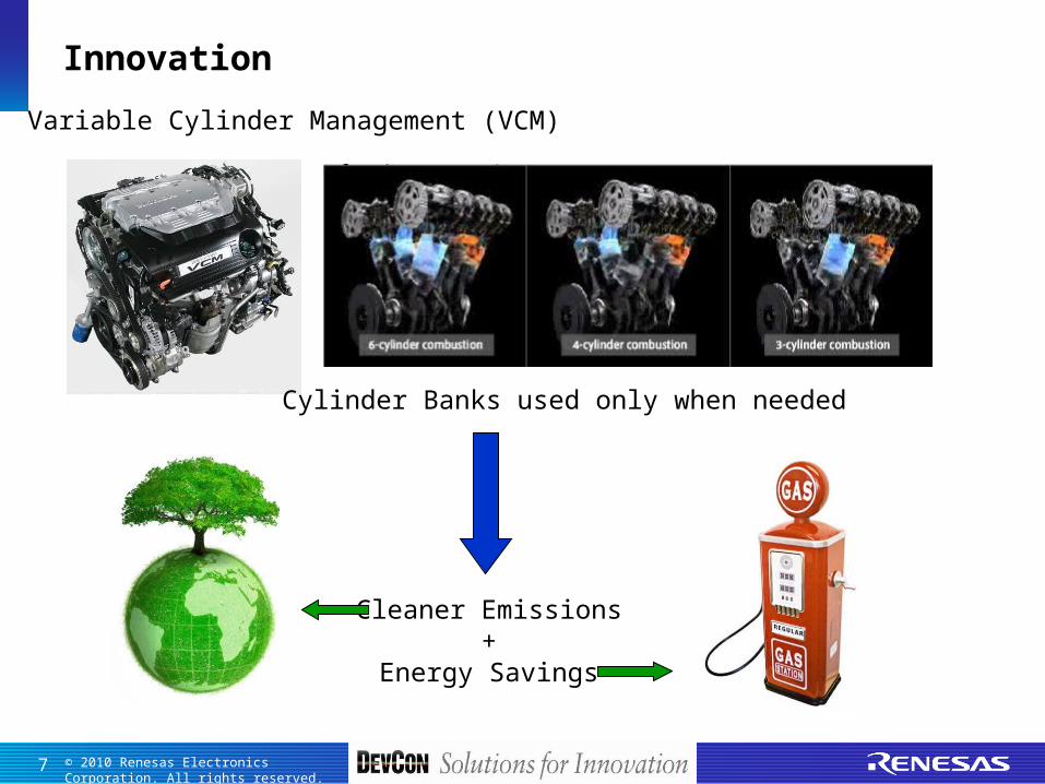
Innovation
Variable Cylinder Management (VCM)
Cleaner Emissions+
Energy Savings
Cylinder Banks used only when needed

© 2010 Renesas Electronics Corporation. All rights reserved.
8
Our Scalable Solution
Renesas provides a flexible solution for managing high-current
applications which maximizes efficiency by intelligently
managing power to the various system rails. Much like
individual cylinders are activated and de-activated in the
Variable Cylinder Management engine technology, banks of
single packaged Point-of-Load (POL) devices are turned on and
off depending on the system’s power requirement for each of
the power rails at any given time.

© 2010 Renesas Electronics Corporation. All rights reserved.
9
Agenda
What is POL-SiP (point-of-load system-in-package)?
Scalable VR Concept and Architecture
Advantages of MCU Control and POL-SiP Devices
System Sensing, Monitoring, and Control
Overview of EVB and Software Control through GUI
Lab
System bring-up
Programming through GUI
System monitoring and control

© 2010 Renesas Electronics Corporation. All rights reserved.
10
Key Takeaways
By the end of this session you will be able to:
Understand POL-SiP concept
Understand 1-phase, 2-phase VR system by POL-SiP
Understand Scalable VR concept & architecture
Understand Scalable VR advantages
Identify appropriate applications for Scalable VR

© 2010 Renesas Electronics Corporation. All rights reserved.
11
What is a POL-SiP ?
All silicon chips for a Buck Converter in one package!
PWM Control& Gate Drive
External L&C
Top MOS FET
VIN
VOUT
3 chips in ONE package!
Control IC + Top MOS + Bottom MOS = 8mm x 8mm QFN-56
■■
Bottom MOS FET+ SBD
(Schottky Barrier Diode)

© 2010 Renesas Electronics Corporation. All rights reserved.
12
Why POL-SiP ?
1. Large scale Logic IC power requires Low Voltage and High Current
DCDCconverterVin Vcc Load ( IC )
Icc 20W
0
5
10
15
20
25
012345Vcc (V)
Icc
(A)
Low Voltage and High Current
High current density devices are required! POL-SiP
If a 20W load is used, then the
current increases and the voltage
decreases
I = P/V
■■

© 2010 Renesas Electronics Corporation. All rights reserved.
13
Why POL-SiP ?
2. The Vcc range of Large Scale Logic ICs is becoming increasingly narrow
Fast response converters are required
0
1
2
3
4
5
6
00.10.20.30.40.50.6
Process Rule (um)
Co
re v
olt
age
(V)
500mV(0.5um)
300mV(0.35um)
250mV(0.22um)
100mV(65nm)
POL-SiPPeak Current Control Mode
■■

© 2010 Renesas Electronics Corporation. All rights reserved.
14
Features of Renesas POL-SiP(R2J20702NPR2J20702NP)
92.5% @Vin=12V, Vout=1.8V, Fsw=500kHz
Up to 40A output current per device.
Output voltage fluctuation range is 40mV or below
2-phase operation, Current sharing
Peak current mode topology
Huge current
High efficiency
Fast response for transient load
Useful functions
(di/dt=50A/us, 4.5A step)
Over current protection ( Hiccup )
Synchronous operation, Tracking-start
Remote ON/OFF control
For even higher currents:
Easy andSimple
■■
© 2010 Renesas Electronics Corporation. All rights reserved.
15
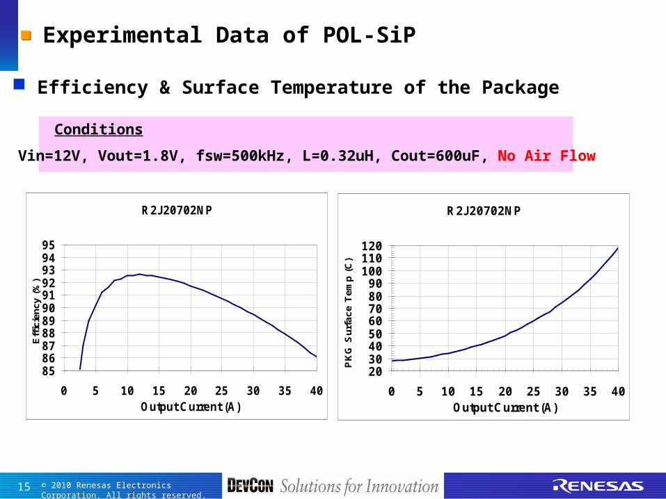
Experimental Data of POL-SiP
Efficiency & Surface Temperature of the Package
Vin=12V, Vout=1.8V, fsw=500kHz, L=0.32uH, Cout=600uF, No Air Flow
Conditions
R2J 20702NP
8586878889909192939495
0 5 10 15 20 25 30 35 40Output Current (A)
Effi
cien
cy (
%)
R2J 20702NP
2030405060708090
100110120
0 5 10 15 20 25 30 35 40Output Current (A)
PK
G S
urfa
ce T
emp
(C)
■■

© 2010 Renesas Electronics Corporation. All rights reserved.
16
Experimental Data of POL-SiP
Transient response
Vin=12V, Vout=1.8V, fsw=468kHz, L=0.32uH, Cout=600uF
Conditions
Iout : 0A <=> 4.5A, Iout slope : 50A/us
30mV
Time (40us/div.)Time (40us/div.)
Vout(AC) Vout(AC)(50mV/div.)(50mV/div.)
30mV
Iout : 0A to 4.5A Iout : 4.5A to 0A
■■

© 2010 Renesas Electronics Corporation. All rights reserved.
17
Various Parallel Operation of POL-SiP
IL2
Iout up to 80A max
180° Phase-shifted
Current Sharing
40A
40A
80A
IL1 IL2
InductorCurrent
IL1
SW node1
SW node2
2-phase operation
synchronization
ex. 2.4V
ex. 1.5V
Synchronous operation
Tracking start
Ratiometric
Coincident
Vout1
Vout2
Vout1
Vout2
Multi-channel operation (ex. 2 channel operation)
(up to 5ch available)
■■

© 2010 Renesas Electronics Corporation. All rights reserved.
18
Evaluation Boards of POL-SiP
R2J20702R2J20702
2 channel EVB
Vin= 12V
Vout_1= 2.5V / Vout_2= 1.8V
Iout_1= 23A / Iout_2= 21A max.
fsw= 480kHz /channel
Default conditions AdjustableAdjustableVin= 12V
Vout= 1.8V
Iout= 20A max.
fsw= 500kHz
Default conditions
AdjustableAdjustable
R2J20702R2J20702
Single phase EVB
Default conditions Vin= 12V
Vout= 1.8V
Iout= 42A max.
fsw= 450kHz / phase
R2J20702R2J20702
AdjustableAdjustable
2 phase EVB
■■

© 2010 Renesas Electronics Corporation. All rights reserved.
19
Design tool
Design guide for loop compensation.
(EXCEL sheet)
■■
Enter into the red framed cells
obtain constants for loop compensation

© 2010 Renesas Electronics Corporation. All rights reserved.
20
Block diagram
ReferenceCurrentGenerator
50k
50k
ActiveCurrentSensing
S
R
Q
Q
OCP Comparator
Error Amp.
OSC
Pulse Generator
RES
Max. Duty
(Bi-lateral)
RES
Max. Duty
50ns
55ns Blanking
UVLO5V (4%)Regulator
ON / OFF
Gate DriveLogicCircuitOCP
PWM
ON / OFF
VIN
BOOTREG5ON/OFF
IREF
CT
SYNC
TRK-SS
FB
EO
Ishare RAMP CS
PGND
SW
SGND
DRV5
Idh
Idh22000
8V to 16V
SBD
VOUT
VOUT
CurrentSenseComparator
REG5
1.5V
OCPHiccupControl
0.6V(1%)
REG5
OCP
ON / OFF
(1024 pulses blank)
VCIN
0.1V
490uA
5.25V (4%)Regulator
DRV5
REG GOOD
REG GOOD
Supervisor
REG GOOD
■■

© 2010 Renesas Electronics Corporation. All rights reserved.
21
AACTIVE CTIVE CCURRENT URRENT SSENSINGENSING
ReferenceCurrentGenerator
50k
50k
ActiveCurrentSensing
S
R
Q
Q
OCP Comparator
Error Amp.
OSC
Pulse Generator
RES
Max. Duty
(Bi-lateral)
RES
Max. Duty
50ns
55ns Blanking
UVLO5V (4%)Regulator
ON / OFF
Gate DriveLogicCircuitOCP
PWM
ON / OFF
VIN
BOOTREG5ON/OFF
IREF
CT
SYNC
TRK-SS
FB
EO
Ishare RAMP CS
PGND
SW
SGND
DRV5
Idh
Idh22000
8V to 16V
SBD
VOUT
VOUT
CurrentSenseComparator
REG5
1.5V
OCPHiccupControl
0.6V(1%)
REG5
OCP
ON / OFF
(1024 pulses blank)
VCIN
0.1V
490uA
5.25V (4%)Regulator
DRV5
REG GOOD
REG GOOD
Supervisor
REG GOOD
■■
0.6V(1%)

© 2010 Renesas Electronics Corporation. All rights reserved.
22
SW voltage(10V/div)
CS voltage(0.5V/div)
Coil current(10A/div) 500ns/div.
Iout=0A Iout=10A Iout=20A
500ns/div.
Vin=12V, Vout=1.8V, Freq=469kHz, L=440nH, Cout=600uF, Rcs=410ohm
The peak voltage of CS pin is proportional to coil current
500ns/div.
AACTIVE CTIVE CCURRENT URRENT SSENSINGENSING
Wave Form
■■

© 2010 Renesas Electronics Corporation. All rights reserved.
23
Item Voltage mode Peak current mode
Loop analysis easy somewhat easy
Loop compensation somewhat complicated simple
Transient response slow fast
Noise immunity good good
Ext synchronization somewhat complicated very easy
Current sharing difficult very easy
Peak current mode = Big advantage
Peak Current Control Mode■■

© 2010 Renesas Electronics Corporation. All rights reserved.
24
Agenda
What is POL-SiP (point-of-load system-in-package)?
Scalable VR Concept and Architecture
Advantages of MCU Control and POL-SiP Devices
System Sensing, Monitoring, and Control
Overview of EVB and Software Control through GUI
Lab
System bring-up
Programming through GUI
System monitoring and control
© 2010 Renesas Electronics Corporation. All rights reserved.
25
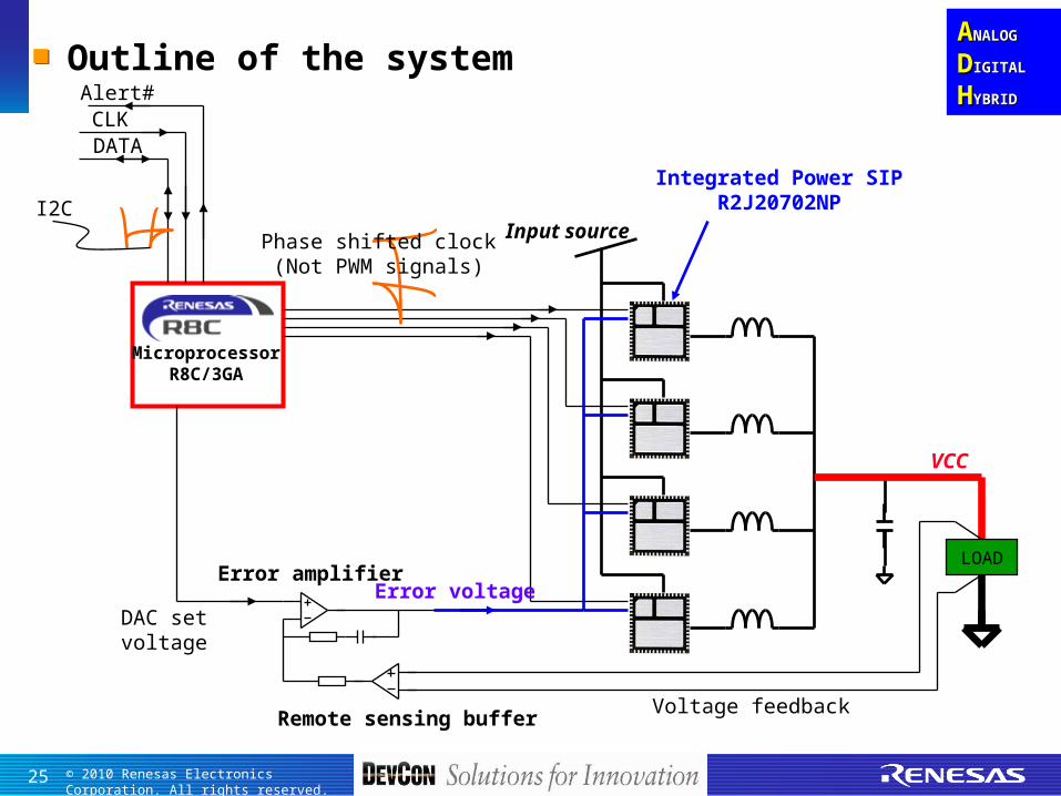
Outline of the system
MicroprocessorR8C/3GA
DATACLKAlert#
VCC
Error amplifier
I2C
Phase shifted clock(Not PWM signals)
DAC setvoltage
Voltage feedback
Error voltage
Input source
Integrated Power SIPR2J20702NP
AANALOGNALOG
DDIGITALIGITAL
HHYBRIDYBRID
LOAD
Remote sensing buffer
■■

© 2010 Renesas Electronics Corporation. All rights reserved.
26
Concept of RENESAS Multi-phase VR by POL-SiP4-phase example
Clock-1
Clock-2
Clock-3
Clock-4
POL- SiP (8x8mm, QFN56)(Not a DrMOS),includes ACS(Active Current Sensing)and PWM modulator.
Error Voltage Bus
No “PWM” signals fed to POL-SIPs, only need phase shifted clock signals.Each POL-SIP is like a cylinder in VCM, MCU adds or sheds POL-SIPs to optimize load efficiency or performance as required
FromMCU
Error Amp.
■■

© 2010 Renesas Electronics Corporation. All rights reserved.
27
Agenda
What is POL-SiP (point-of-load system-in-package)?
Scalable VR Concept and Architecture
Advantages of MCU Control and POL-SiP Devices
System Sensing, Monitoring, and Control
Overview of EVB and Software Control through GUI
Lab
System bring-up
Programming through GUI
System monitoring and control

© 2010 Renesas Electronics Corporation. All rights reserved.
28
Key Highlights of RENESAS Hybrid Power Solution
Eliminates need for PWM control IC
Digital interface to host CPU - I2C - Vout control, status report, etc. Design flexibility - GUI
Fast transient response - Analog PWM (Peak current mode) - Output current sensing built-in Efficiency Boost - Copper Clip Bonding - New SBD JET MOSFET built-in
MicrocontrollerTechnology
Integrated Power SIPTechnology
AANALOGNALOG
DDIGITALIGITAL
HHYBRIDYBRID
New R8C/3GA
New R2J20702NP
■■

© 2010 Renesas Electronics Corporation. All rights reserved.
29
What’s NEW of Renesas Scalable VR solution
Tiny MCU (R8Cxx) POL-SiP (R2J20702NP)
• Serial Interface to main CPU• VR master control (VID, Phase)• Monitors (Io, Vo, Temp, etc)• Adaptive Control by S/W• High resolution Calibration
• VR slave driving• High Power Up to Io=40A/ch• High Efficiency• High fpwm Up to 1MHz• Current sensing built-in
■■

© 2010 Renesas Electronics Corporation. All rights reserved.
30
Agenda
What is POL-SiP (point-of-load system-in-package)?
Scalable VR Concept and Architecture
Advantages of MCU Control and POL-SiP Devices
System Sensing, Monitoring, and Control
Overview of EVB and Software Control through GUI
Lab
System bring-up
Programming through GUI
System monitoring and control

© 2010 Renesas Electronics Corporation. All rights reserved.
31
An example of a conventional V-mode controlled buck converter
Analog Digital Hybrid, C-mode controlled buck converterAnalog Digital Hybrid, C-mode controlled buck converter AA N A L O GN A L O G
DD I G I T A LI G I T A L
HH Y B R I DY B R I D
LOAD
DriverPWMControlCircuitry
Current informationVoltage feedback
PWM Signal
PWM SignalsFor other phases
Vin
Vcc
- Difficult to use a digital interface.- Complex PWM circuit required as phase number increases.
RENESAS Scalable VR by POL- SIP■■
LOAD
Current sense, PWM control,and Drive
Pulse generate,Analog error amp.,Circuitry
Voltage feedback
Clock pulse
Phase shifted clock For other phases
Vin
Vcc
Error voltage bus (Current information)
POL-SIP product.
P/N : R2J20702NP IntegratedPower SIP
Easy to accomplish with an MCU and simple analog components.

© 2010 Renesas Electronics Corporation. All rights reserved.
32
ACS for Peak Current Mode Control, OCP, L/L control and current sharing
Voltage Mode (Conventional)Generated PWM signal compared with Triangle wave and Error Voltage
Triangle wave Error Voltage
PWM
Reference Voltage
Triangle Wave
Feedback Voltage
PWMError Amp
PWM Comparator
Peak Current Mode (Proposed)Generated PWM signal compared with Choking Coil Current and Error Voltage
Choking Coil Current by ACS
PWM
Clock
Reference Voltage
Choking CoilCurrent
Feedback Voltage
PWM
Error amp
PWM Comparator
S
RQ#
ClockNeed current sensing circuit for over-current protection, light load control and current balance
Slow response Fast response
■■ RENESAS Scalable VR by POL- SIP
Error Voltage

© 2010 Renesas Electronics Corporation. All rights reserved.
33
DCR Sensing (Current)
Detect Output current using voltage drop of choking coil
PTC
PWM
Current sense
Active Current Sensing (Original)
Detect Output current using Sensing MOSFET in POL-SIP
Driver+FETs
Poor accuracy
Large Temperature dependency
Difficult to use small DCR choking coil
Larger PCB space required
Higher PCB thermal resistance Possible destruction of high side FET
High Accuracy (+/-5%)
No Temperature dependency
Can use small DCR choking coil
Less PCB space required
Lower PCB thermal resistance
High side FET never blows up
PWM IC
ACSCurrentSignal
MCUClock
POL-SIP
■■ RENESAS Scalable VR by POL- SIP

© 2010 Renesas Electronics Corporation. All rights reserved.
34
Iout Accuracy Target (2-phase)
0
10
20
30
40
50
60
70
80
0 20 40 60 80 100 120
VR Load (%)
Iou
t A
cc
ura
cy
(%
)
DCR ACS
DCR Sensing (Current)
PTC
PWM
Current sense Input Offset = +/-1mV
Active Current Sensing (Original)
Driver+FETsPWM IC
ACSCurrentSignal
MCUClock
POL-SIP
DCR=0.4mohm+/-8%
Current sense AmpGain deviation=+/-3%
Rex=470ohm+/-1%
ACS deviation=+/-5%
45-60A (typical)
DCR SensingDCR Sensing
ACS SensingACS Sensing
In this example, DCR Sensing does NOT consider:
DCR Temp dependency
NTC (thermistor) mismatching
sL/Rdc, sRcsCcs mismatching
Noise interference
If these items were considered, the accuracy would be worse.
Rcs Ccs
L+Rdc
■■ RENESAS Scalable VR by POL- SIP

© 2010 Renesas Electronics Corporation. All rights reserved.
35
Agenda
What is POL-SiP (point-of-load system-in-package)?
Scalable VR Concept and Architecture
Advantages of MCU Control and POL-SiP Devices
System Sensing, Monitoring, and Control
Overview of EVB and Software Control through GUI
Lab
System bring-up
Programming through GUI
System monitoring and control

© 2010 Renesas Electronics Corporation. All rights reserved.
36
6-phase VR
MCUR8C/2A
Example 1: Scalable VR 6-phase VR Evb■■

© 2010 Renesas Electronics Corporation. All rights reserved.
37
VID Monitor
Voltage Control
Voltage Control
Voltage Control
Example 1: Scalable VR 6-phase VR Block Diagram
……
Phase Control2
Phase Control1
Phase Control6
Enable2
Enable1
Enable6
POL-SiP2
POL-SiP6
VRM MCU(R8C/2A)
VPROTECT
VLOCAL
VS
EN
SE
LO
AD
Temperature
POL-SiP1
Vin_12V
MasterMCU
I2C,SMBus,PMBus
Output Current1
(Io=150A)6-Phase VR
■■

© 2010 Renesas Electronics Corporation. All rights reserved.
38
6-Phase Efficiency (%)
50
60
70
80
90
100
0 10 20 30 40 50 60 70 80 90 100
110
120
130
140
150
IOUT (A)
Eff
icie
ncy
(%
)
Efficiency(%)
VIN=12VVOUT=1.2V6-phasefPWM=540KHz300LFM AirflowNo heatsink
Master MCU R8C/2A + Slave POL-SiP R2J20702NP x6
Example 1: Scalable VR 6-phase VR Result■■

© 2010 Renesas Electronics Corporation. All rights reserved.
39
AANALOGNALOG
DDIGITALIGITAL
HHYBRIDYBRID
VR
+12V input
LOAD1.5V (80A)
PC
RS-232C
+5V input (for MCU)
I2C ~ RS232 interface circuitry
I2C port
LCD interface port (optional)
Example 2: Scalable VR 4-phase VR Evb■■

© 2010 Renesas Electronics Corporation. All rights reserved.
40
MicroprocessorR8C/3GA
DATACLKAlert#
VCC
Error amplifier
I2C
Phase shifted clock(Not PWM signals)
DAC setvoltage
Voltage feedback
Error voltage
Input source
Integrated Power SIPR2J20702NP
AANALOGNALOG
DDIGITALIGITAL
HHYBRIDYBRID
LOAD
Remote sensing buffer
Example 2: Scalable VR 4-phase VR Block Diagram■■

© 2010 Renesas Electronics Corporation. All rights reserved.
41
I2C serial communication
Four phase VR in 2.5” x 1”
Power Spec.• Vin = 12V typical• Vout = 1.5V• Iout = 80A• Freq = 500kHz• Efficiency >90% @ 80A• Load step +/-2.5% @ 30A step,
30A/us• Ripple voltage 15mVpp
AANALOGNALOG
DDIGITALIGITAL
HHYBRIDYBRID
Graphic interface• RS232C• Adjustable: Vout, Freq, Number of
phases• Monitor: Vin, Vout, Iin, Iout, Temp• Protection: OVP, OCP, OTP
2.5 inch
1 inch
Back side
POL-SIP
Example 2: Scalable VR 4-phase VR Specification■■

© 2010 Renesas Electronics Corporation. All rights reserved.
42
AANALOGNALOG
DDIGITALIGITAL
HHYBRIDYBRIDCondition; Vin=12V, Vo=1.5V, Freq=500kHz
Efficiency vs. Load current
85
86
87
88
89
90
91
92
0 10 20 30 40 50 60 70 80 90 100
Load current(A)
Effi
ciency
(%
)
SheddingNoAirflow
SheddingAirflow
Example 2: Scalable VR 4-phase VR Efficiency■■

© 2010 Renesas Electronics Corporation. All rights reserved.
43
AANALOGNALOG
DDIGITALIGITAL
HHYBRIDYBRIDCondition; Vin=12V, Vo=1.5V, Freq=300kHz and 500kHz Airflow=300LFM
Efficiency vs. Load current
85
86
87
88
89
90
91
92
93
0 10 20 30 40 50 60 70 80 90 100
Output current(A)
Eff
icency(%
)
Fsw=500KHz
Fsw=300KHz
Example 2: Scalable VR 4-phase VR Efficiency■■

© 2010 Renesas Electronics Corporation. All rights reserved.
44
AANALOGNALOG
DDIGITALIGITAL
HHYBRIDYBRIDCondition; Vin=12V, Vo=1.5V, Freq=500kHz
Package temperature vs. Load current
0
10
20
30
40
50
60
70
80
90
100
0 10 20 30 40 50 60 70 80 90 100
Load current(A)
Te
mp
era
ture
(de
gC
)
SheddingNoAirflow
SheddingAirflow
Example 2: Scalable VR 4-phase VR PKG Temp.■■

© 2010 Renesas Electronics Corporation. All rights reserved.
45
AANALOGNALOG
DDIGITALIGITAL
HHYBRIDYBRID
1phase 10A
4phase 40A
2phase 20A
4phase 80A
15mVpp 6mVpp
7mVpp 6mVpp
Condition; Vin=12V, Vo=1.5V, Freq=500kHz
Example 2: Scalable VR 4-phase VR Output Ripple■■10
mV
/div
10m
V/d
iv
10m
V/d
iv
10m
V/d
iv
1µs/div
1µs/div 1µs/div
1µs/div

© 2010 Renesas Electronics Corporation. All rights reserved.
46
AANALOGNALOG
DDIGITALIGITAL
HHYBRIDYBRID
Load freq.=1kHz
Load freq.=100kHz
Load freq.=10kHz
Load freq.=500kHz
76mVpp 68mVpp
58mVpp 30mVpp
Condition; Vin=12V, Vo=1.5V, Freq=500kHz, Io=0-30A(30A/us)
Example 2: Scalable VR 4-phase VR Load Transient■■50
mV
/div
50m
V/d
iv
50m
V/d
iv
50m
V/d
iv
100µs/div 50µs/div
5µs/div 2µs/div

© 2010 Renesas Electronics Corporation. All rights reserved.
47
Test environment for load transient testAANALOGNALOG
DDIGITALIGITAL
HHYBRIDYBRID
+5V input To DMM+12V input
Probe
The wires should be as short as possible so that minimize parasitic inductance.
Electrical Load (Keisoku-Giken)
■■

© 2010 Renesas Electronics Corporation. All rights reserved.
486
VR(2” x 1”)
+12V input
LOAD1.5V (80A)
PC
RS-232C
+5V input (for MCU)
I2C ~ RS232 interface circuitry
I2C port
LCD interface port (optional)
GUI
GUI (Graphic User Interface) … Controlled by PC■■

© 2010 Renesas Electronics Corporation. All rights reserved.
496
GUI (Graphic User Interface) … setting parameters■■

© 2010 Renesas Electronics Corporation. All rights reserved.
506
GUI (Graphic User Interface) … VR operating■■

© 2010 Renesas Electronics Corporation. All rights reserved.
516
GUI (Graphic User Interface) … OCP example■■

© 2010 Renesas Electronics Corporation. All rights reserved.
526
GUI (Graphic User Interface) … real time monitor
VOUT monitor window
IOUT monitor window
Temperature monitor window
OVP level
OCP level
■■

© 2010 Renesas Electronics Corporation. All rights reserved.
53
Agenda
What is POL-SiP (point-of-load system-in-package)?
Scalable VR Concept and Architecture
Advantages of MCU Control and POL-SiP Devices
System Sensing, Monitoring, and Control
Overview of EVB and Software Control through GUI
Lab
System bring-up
Programming through GUI
System monitoring and control

© 2010 Renesas Electronics Corporation. All rights reserved.
54
Questions?
What are the merits of an integrated solution, such as Renesas POL-SiP, versus a discrete solution?
Why is scalability important for VR design?
What are some advantages of Active Current Sensing(ACS)?
Audience Questions?

© 2010 Renesas Electronics Corporation. All rights reserved.
55
Our Scalable Solution
Renesas provides a flexible solution for managing high-current
applications which maximizes efficiency by intelligently
managing power to the various system rails. Much like
individual cylinders are activated and de-activated in the
Variable Cylinder Management engine technology, banks of
single packaged Point-of-Load (POL) devices are turned on and
off depending on the system’s power requirement for each of
the power rails at any given time.
© 2010 Renesas Electronics Corporation. All rights reserved. Renesas Confidential56
Thank You!

© 2010 Renesas Electronics Corporation. All rights reserved. Renesas Confidential57
Appendix