4 Branches of Earth Science Preview Activity for Monday’s Lab! Team 6-B Science!!! Pairs Activity!
date post
20-Dec-2015Category
view
214download
0
Reaction rates are influenced by
A. activation energy
B. temperature
C. relative abundance of reactants
D. all of the above
Monday’s Unregistered clickers:1B37B39F 1B462578 1B3E85A0

Catalysts speed up reactions but are not used up
A.true
B. false
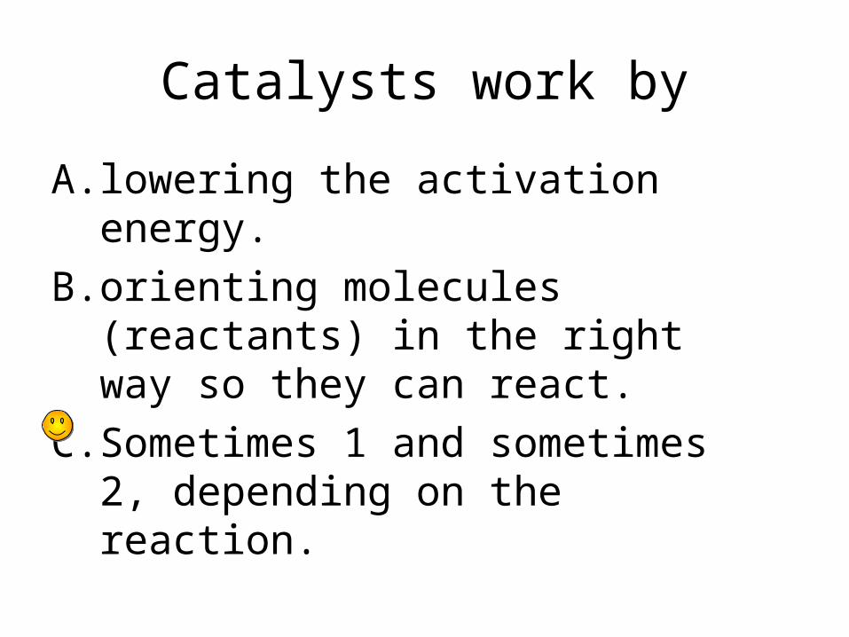
Catalysts work by
A. lowering the activation energy.
B. orienting molecules (reactants) in the right way so they can react.
C. Sometimes 1 and sometimes 2, depending on the reaction.

reduce activation energy
the right orientation

Chemical reactions happen in order to
A. increase entropy
B. decrease energy
C. some combination of 1 and 2

• What are these bonds like?
• How does the wave model explain all this?
Bonding in Metals, Alloys,
and Semiconductors
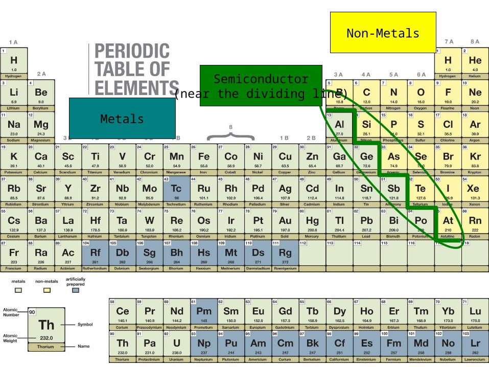
Metals
Non-Metals
Semiconductor(near the dividing line)

s pd
f

metals
• bonding deals with the valence electrons.
• metals have mostly empty orbitals.
• metals have low ionization energies
• electrons want to be in the lowest possible energy states
s pd
f

metals
• bonding deals with the valence electrons.
• metals have mostly empty orbitals.
• metals have low ionization energies
• electrons want to be in the lowest possible energy states
• When 2 atoms get close together, new molecular orbitals form
2 atoms and the wave model
two separated atoms
two atoms in a molecule
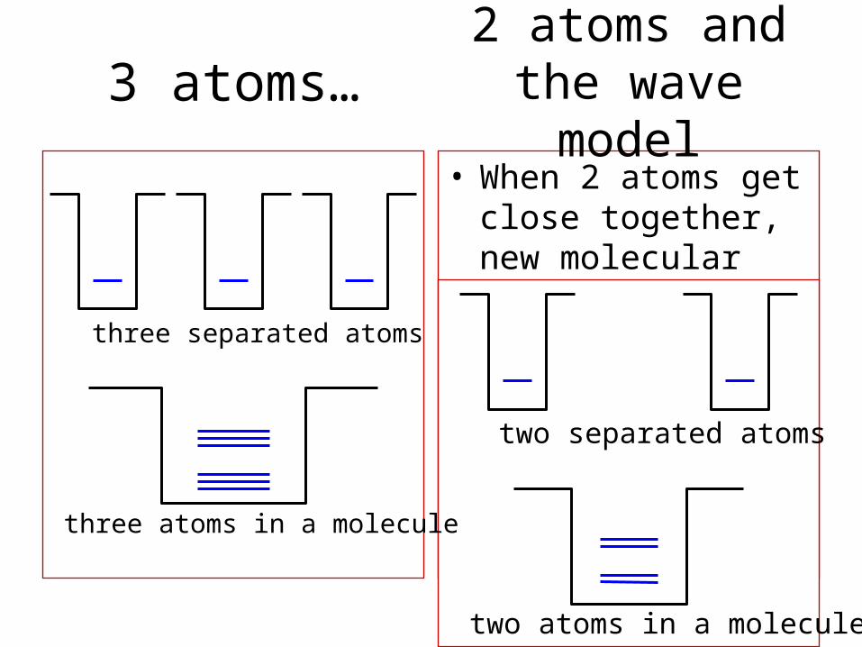
3 atoms…
• When 2 atoms get close together, new molecular orbitals form
2 atoms and the wave model
two separated atoms
two atoms in a molecule
three separated atoms
three atoms in a molecule

3 atoms…
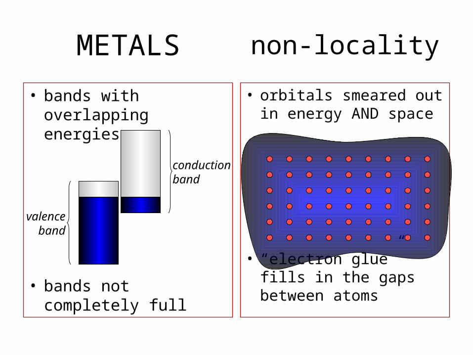
• energy of molecular orbitals overlap
• ENERGY BANDS
a jillion atoms
energy bands in a solid
three separated atoms
three atoms in a molecule
valence band
conduction band

• bands with overlapping energies
• bands not completely full
METALS
• energy of molecular orbitals overlap
• ENERGY BANDS
a billion atoms
energy bands in a solid
valence band
conduction bandvalence
band
conductionband
• bands with overlapping energies
• bands not completely full
METALS
• orbitals smeared out in energy AND space
• “electron glue” fills in the gaps between atoms
non-locality
valenceband
conductionband

• metals are…– malleable– electrical conductors– thermal conductors – opaque– reflective
Metallic properties
• orbitals smeared out in energy AND space
• “electron glue” fills in the gaps between atoms
non-locality
Most also melt at higher temperatures
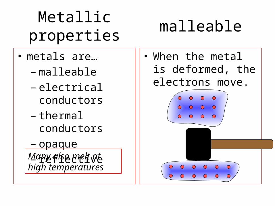
• metals are…– malleable– electrical conductors– thermal conductors – opaque– reflective
Metallic properties
• When the metal is deformed, the electrons move.
malleable
Many also melt at high temperatures
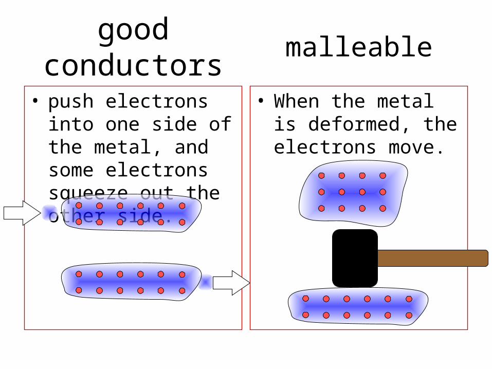
• push electrons into one side of the metal, and some electrons squeeze out the other side.
good conductors
• When the metal is deformed, the electrons move.
malleable

According to the wave model of the atom, how does a single atom absorb a photon?
A. An atom can absorb light of any wavelength.
B. An atom absorbs light when the photon energy equals the energy difference between orbitals.
C. An atom changes its internal state to match the photon energy.

• For visible light, there are MANY empty orbitals.
• The metal absorbs a photon and an electron jumps up to an un-filled orbital
opaque
• The excited electron falls back down to the lowest possible energy state
• It emits a photon like the one it absorbed
reflective
photonin
electronexcited
electronfalls
photonemitted
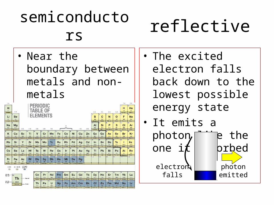
• Near the boundary between metals and non-metals
semiconductors
• The excited electron falls back down to the lowest possible energy state
• It emits a photon like the one it absorbed
reflective
electronfalls
photonemitted

• Near the boundary between metals and non-metals
semiconductors
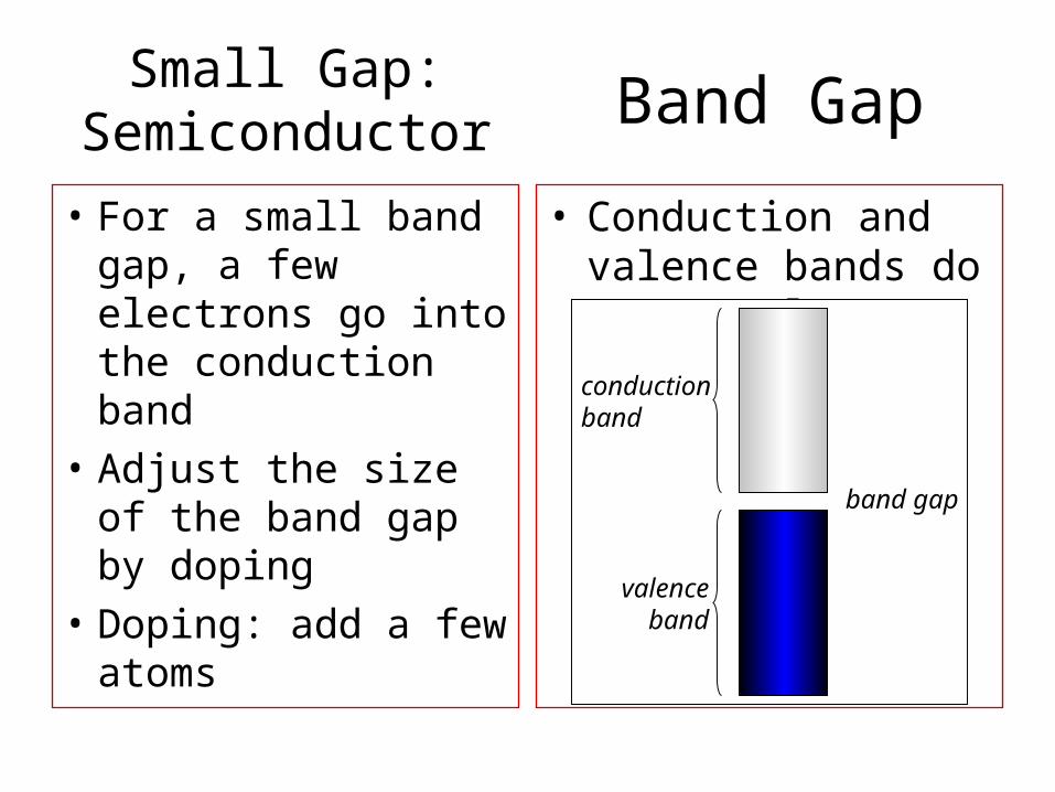
• Conduction and valence bands do not overlap
Band Gap
valenceband
conductionband
band gap

• For a small band gap, a few electrons go into the conduction band
• Adjust the size of the band gap by doping
• Doping: add a few atoms
Small Gap:Semiconductor
• Impurity atoms stress the network
• Stresses change energy levels and band gap
• Different Gap: different colors
Doping
• For a small band gap, a few electrons go into the conduction band
• Adjust the size of the band gap by doping
• Doping: add a few atoms
Small Gap:Semiconductor
• Conduction and valence bands do not overlap
Band Gap
valenceband
conductionband
band gap

• atoms and electrons have different speed distributions
Thermal Excitation
• Impurity atoms stress the network
• Stresses change energy levels and band gap
• Different Gap: different colors
Doping
atoms
electrons
valenceband
conductionband
gap