Questions and Solution - Navodaya Institute of …€¦ · · 2015-10-01Implement the basic gates...
61
Logic Design 10ES33 Page 1 Questions and Solution Unit 1 Principles of combinational logic- 1 1. Using Karnaugh Map,simplify the following boolean expression and give the implementation of the same using i)NAND gates only(SOP) ii) NOR gates only (POS ) a. F(w,x,y,z)=m(0,1,2,4,5,12,14)+dc(8,10) F(w,x,y,z)=m(0,1,2,4,5,12,14)+dc(8,10) (June /July 2015) (Dec 13/ Jan14) 8 Marks a. NAND Gate (SOP form) C’D’ C’D CD CD’ A’B’ 1 1 1 A’B 1 1 AB 1 1 AB’ X X F(A,B,C,D) = C’D’ + A’C’ + AD’ + B’D’ b. NOR gate (POS form) F(A,B,C,D) = (A + C)(C+D)(A’+D)(B+D) 2. Explain Duality Theorem? (Dec 13/ Jan14) 4 Marks One can transform the given expression by interchanging the operation (+) and (•) as well as the identity elements 0 and 1 . Then the expression will be referred as dual of each other. This is known as the principle of duality. Example x + x = 1 then the dual expression is x • x = 0 3. What are Universal gates? Implement the basic gates using Universal gates only. (Dec 14/Jan 15) (Dec 13/ Jan14) 8 Marks
Transcript of Questions and Solution - Navodaya Institute of …€¦ · · 2015-10-01Implement the basic gates...

Logic Design 10ES33
Page 1
Questions and Solution
Unit 1
Principles of combinational logic- 1
1. Using Karnaugh Map,simplify the following boolean expression and give the
implementation of the same using i)NAND gates only(SOP) ii) NOR gates only (POS )
a. F(w,x,y,z)=m(0,1,2,4,5,12,14)+dc(8,10)
F(w,x,y,z)=m(0,1,2,4,5,12,14)+dc(8,10)
(June /July 2015) (Dec 13/ Jan14) 8 Marks
a. NAND Gate (SOP form)
C’D’ C’D CD CD’
A’B’ 1 1 1
A’B 1 1
AB 1 1
AB’ X X
F(A,B,C,D) = C’D’ + A’C’ + AD’ + B’D’
b. NOR gate (POS form)
F(A,B,C,D) = (A + C)(C+D)(A’+D)(B+D)
2. Explain Duality Theorem? (Dec 13/ Jan14) 4 Marks
One can transform the given expression by interchanging the operation (+) and (•)
as well as the identity elements 0 and 1 . Then the expression will be referred as
dual of each other. This is known as the principle of duality.
Example x + x = 1 then the dual expression is x • x = 0
3. What are Universal gates? Implement the basic gates using Universal gates only.
(Dec 14/Jan 15) (Dec 13/ Jan14) 8 Marks
Logic Design 10ES33
Page 2
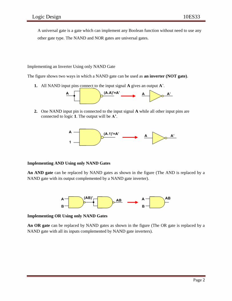
A universal gate is a gate which can implement any Boolean function without need to use any
other gate type. The NAND and NOR gates are universal gates.
Implementing an Inverter Using only NAND Gate
The figure shows two ways in which a NAND gate can be used as an inverter (NOT gate).
1. All NAND input pins connect to the input signal A gives an output A’.
2. One NAND input pin is connected to the input signal A while all other input pins are
connected to logic 1. The output will be A’.
Implementing AND Using only NAND Gates
An AND gate can be replaced by NAND gates as shown in the figure (The AND is replaced by a
NAND gate with its output complemented by a NAND gate inverter).
Implementing OR Using only NAND Gates
An OR gate can be replaced by NAND gates as shown in the figure (The OR gate is replaced by a
NAND gate with all its inputs complemented by NAND gate inverters).

Logic Design 10ES33
Page 3
Thus, the NAND gate is a universal gate since it can implement the AND, OR and NOT
functions.
NAND Gate is a Universal Gate:
To prove that any Boolean function can be implemented using only NOR gates, we will show
that the AND, OR, and NOT operations can be performed using only these gates.
Implementing an Inverter Using only NOR Gate
The figure shows two ways in which a NOR gate can be used as an inverter (NOT gate).
.
Implementing OR Using only NOR Gates
An OR gate can be replaced by NOR gates as shown in the figure (The OR is replaced by a NOR
gate with its output complemented by a NOR gate inverter)
Implementing AND Using only NOR Gates
An AND gate can be replaced by NOR gates as shown in the figure (The AND gate is replaced by a
NOR gate with all its inputs complemented by NOR gate inverters)

Logic Design 10ES33
Page 4
4. Name universal gates. Realize basic gates using NAND Gates. (July 13) 10 Marks
Universal Gates are : NAND ,NOR
5. Explain positive and negative logic (July 13) 10 Marks
Positive Logic: With reference to positive logic, logical 1 state is the most positive logic or
voltage level and logic 0 state is the most negative logic or voltage level. In other words, active
high level is 1 and active low level is 0. For instance, V(0) = 0V and V(1) = 5V, V(0) = 5V and
V(1) = 15V.

Logic Design 10ES33
Page 5
Negative Logic: With reference to negative logic, logic 0 state is the most positive logic or
voltage level and logic 1 state is the most positive logic or voltage level. In other words, active
high level is 0 and active low level is 1. For instance, V(0) = 5V and V(1) = 0V, V(0) = 15V and
V(1) = 5V.
6. Explain different models for writing Verilog modules. Give an example for each.
(Dec 13/Jan 14) 12 Marks
A module is the building block in Verilog. It is declared by the keyword module and is
always terminated by the keyword endmodule.Each statement is terminated with a
semicolon, but there is no semi-colon after endmodule.
A module can be described in any one (or a combination) of the following modeling
techniques.
Gate-level modeling using instantiation of primitive gates and user defined
modules.
This describes the circuit by specifying the gates and how they are
connected with each other.
Dataflow modeling using continuous assignment statements with the keyword
assign.
This is mostly used for describing combinational circuits.
Behavioral modeling using procedural assignment statements with keyword
always.
This is used to describe digital systems at a higher level of abstraction.

Logic Design 10ES33
Page 6
Gate-level modeling: Here a circuit is specified by its logic gates and their interconnections.
It provides a textual description of a schematic diagram.
Verilog recognizes 12 basic gates as predefined primitives.
4 primitive gates of 3-state type.
Other 8 are: and, nand, or, nor, xor, xnor, not, buf
//Gate-level hierarchical description of 4-bit adder
module halfadder (S,C,x,y);
input x,y;
output S,C;
//Instantiate primitive gates
xor (S,x,y);
and (C,x,y);
endmodule
Dataflow Modeling: Dataflow modeling uses continuous assignments and the keyword
assign.A continuous assignment is a statement that assigns a value to a net. The value assigned
to the net is specified by an expression that uses operands and operators.
//Dataflow description of a 2-to-4-line decoder
module decoder_df (A,B,E,D);
input A,B,E;
output [0:3] D;
assign D[0] = ~(~A & ~B & ~E),
D[1] = ~(~A & B & ~E),
D[2] = ~(A & ~B & ~E),
D[3] = ~(A & B & ~E);

Logic Design 10ES33
Page 7
endmodule
Behavioral Modeling : Behavioral modeling represents digital circuits at a functional and
algorithmic level.
It is used mostly to describe sequential circuits, but can also be used to describe
combinational circuits.
Behavioral descriptions use the keyword always followed by a list of procedural
assignment statements.
The target output of procedural assignment statements must be of the reg data type.
A reg data type retains its value until a new value is assigned.
//Behavioral description of 2-to-1-line multiplexer
module mux2x1_bh(A,B,select,OUT);
input A,B,select;
output OUT;
reg OUT;
always @(select or A or B)
if (select == 1) OUT = A;
else OUT = B;
endmodule
7. Define Logic. Explain different types of logic. ( July 13) 10 Marks
Positive Logic: With reference to positive logic, logical 1 state is the most positive logic or
voltage level and logic 0 state is the most negative logic or voltage level. In other words,
active high level is 1 and active low level is 0. For instance, V(0) = 0V and V(1) = 5V,
V(0) = 5V and V(1) = 15V.

Logic Design 10ES33
Page 8
Negative Logic: With reference to negative logic, logic 0 state is the most positive logic or
voltage level and logic 1 state is the most positive logic or voltage level. In other words,
active high level is 0 and active low level is 1. For instance, V(0) = 5V and V(1) = 0V,
V(0) = 15V and V(1) = 5V.
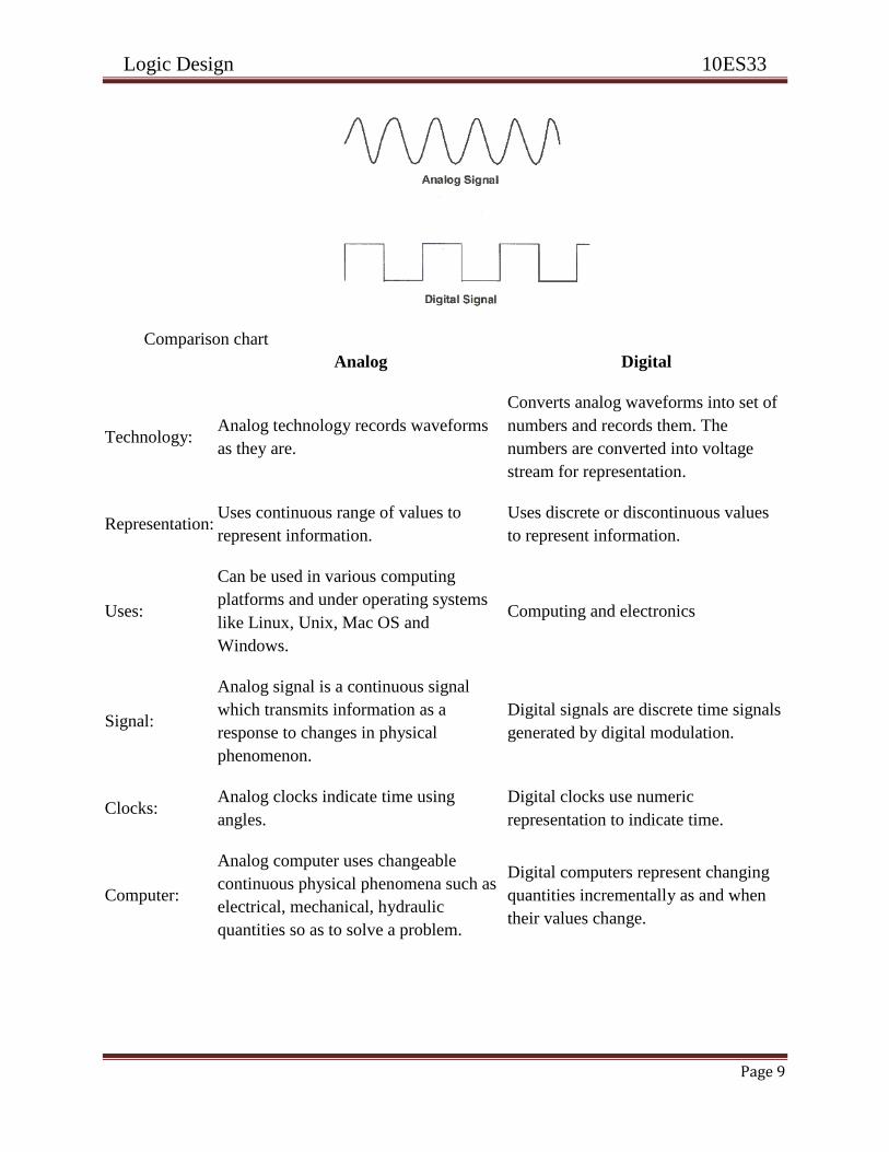
8. Differentiate between Analog and Digital Signals. ( July 13) 10 Marks
An Analog signal is any continuous signal for which the time varying feature (variable) of
the signal is a representation of some other time varying quantity, i.e., analogous to another
time varying signal. It differs from a digital signal in terms of small fluctuations in the
signal which are meaningful.
A digital signal uses discrete (discontinuous) values. By contrast, non-digital (or analog)
systems use a continuous range of values to represent information. Although digital
representations are discrete, the information represented can be either discrete, such as
numbers or letters, or continuous, such as sounds, images, and other measurements of
continuous systems.
Logic Design 10ES33
Page 9
Comparison chart
Analog Digital
Technology: Analog technology records waveforms
as they are.
Converts analog waveforms into set of
numbers and records them. The
numbers are converted into voltage
stream for representation.
Representation: Uses continuous range of values to
represent information.
Uses discrete or discontinuous values
to represent information.
Uses:
Can be used in various computing
platforms and under operating systems
like Linux, Unix, Mac OS and
Windows.
Computing and electronics
Signal:
Analog signal is a continuous signal
which transmits information as a
response to changes in physical
phenomenon.
Digital signals are discrete time signals
generated by digital modulation.
Clocks: Analog clocks indicate time using
angles.
Digital clocks use numeric
representation to indicate time.
Computer:
Analog computer uses changeable
continuous physical phenomena such as
electrical, mechanical, hydraulic
quantities so as to solve a problem.
Digital computers represent changing
quantities incrementally as and when
their values change.

Logic Design 10ES33
Page 10
9. Using Karnaugh Map,simplify the following boolean expression and give the
implementation of the same using
i)NAND gates only(SOP) ii) NOR gates only (POS )
a. F(w,x,y,z)=m(0,1,2,4,5,12,14)+dc(8,10)
F(w,x,y,z)=m(0,1,2,4,5,12,14)+dc(8,10) (Dec 13 / Jan 14) 10 Marks
a. NAND Gate (SOP form)
C’D’ C’D CD CD’
A’B’ 1 1 1
A’B 1 1
AB 1 1
AB’ X X
F(A,B,C,D) = C’D’ + A’C’ + AD’ + B’D’
b. NOR gate (POS form)
F(A,B,C,D) = (A + C)(C+D)(A’+D)(B+D)
10. Mention the Universal gates? Implement with respect to the basic gates .
(June 13) 10 Marks
Universal Gates are : NAND ,NOR

Logic Design 10ES33
Page 11
Unit-2
Principles of combinational logic- 2
1. Implement the following SOP function
F = XZ + Y’Z + X’YZ Compare TTL and CMOS families and the integration
level of ICs (Dec 13/ Jan14) 10 Marks
The Comparison of TTL and CMOS is clearly illustrated in the following table as an example of
differences in the logic families:
TTL CMOS
• Faster
• Stronger drive
capability
• Low power consumption
• Simpler to make
• Greater packing density
• Better noise immunity
Integration Levels:
The devices greatly differ in the density of fabrication ie the levels of integration
used.Depending on the number of transistors/diodes/gates used in the chip they are broadly
classified as :
• SSI -small scale integration
• MSI -medium scale integration
• LSI -large scale integration
• VLSI -very large scale integration
• ULSI -ultra large scale integration
• GSI -giant scale integratio

Logic Design 10ES33
Page 12
Levels of
integration
Transistors/package Gates/chip Applications
SSI 1-100 <12 Logic gates Op-amps
MSI 100-1000 12-99 Registers Filters
LSI 1000-10000 1000 8 bit processor, A/D converter
2. Prove that ABC + ABC' + AB'C + A'BC = AB + AC + BC.(Dec 13/ Jan14) 10 Marks
ABC + ABC' + AB'C + A'BC
=AB(C + C') + AB'C + A'BC
=AB + AB'C + A'BC =A(B + B'C) + A'BC
=A(B + C) + A'BC
=AB + AC + A'BC
=B(A + C) + AC
=AB + BC + AC
=AB + AC +BC ...Proved
3. Find the prime implicant with the help of Qunie-Mc Clusky Method.
Y=f(a,b,c,d)= (0,1,2,6,7,9,10,12)+d(3,5) (Dec 14/Jan 15)(July 15)10 Marks
VLSI 10k gates/chip 16,32 bit processor
256KB memory
DS processor
ULSI 100k gates/chip 64 bit processor
8 MB memory
Image processor
GSI 1M gates/chip 64 MB memory
multiprocessor

Logic Design 10ES33
Page 13
No W X Y Z Index
1 0 0 0 1 1
3 0 0 1 1 2
6 0 1 1 0 2
7 0 1 1 1 3
8 1 0 0 0 1
9 1 0 0 1 2
10 1 0 1 0 2
12 1 1 0 0 2
13 1 1 0 1 3
14 1 1 1 0 3
13 1 1 0 1 3
14 1 1 1 0 3
List the minterm in increasing order of their index
No W X Y Z Index
1 0 0 0 1 1
8 1 0 0 0 1
3 0 0 1 1 2
6 0 1 1 0 2
9 1 0 0 1 2
10 1 0 1 0 2
12 1 1 0 0 2
7 0 1 1 1 3
13 1 1 0 1 3
14 1 1 1 0 3
No W X Y Z Index
1,3 0 0 _ 1 2
1,9 _ 0 0 1 2
8,9 1 0 0 _ 2
8, 10 1 0 _ 0 2
8,12 1 _ 0 0 2
3,7 0 _ 1 1 3
6,7 0 1 1 _ 3
6,14 _ 1 1 0 3
9,13 1 _ 0 1 3
10,14 1 _ 1 0 3
12,13 1 1 0 _ 3
12,14 1 1 _ 0 3

Logic Design 10ES33
Page 14
Prime Implicant: A’B’D + B’C’D + A’CD + A’BC + BCD’ + AC’ + AD’
4. Define impliant. Explain prime and essential prime implicants with example.
(July 13)10 Marks
In Boolean logic, an implicant is a "covering" (sum term or product term) of one or
more minterms in a sum of products (or maxterms in a product of sums) of a boolean function.
Formally, a product term P in a sum of products is an implicant of the Boolean
function F if P implies F. More precisely:
P implies F (and thus is an implicant of F) if F also takes the value 1 whenever P equals
1.
where
F is a Boolean function of n variables.
P is a product term.
A prime implicant of a function is an implicant that cannot be covered by a more
general (more reduced - meaning with fewer literals) implicant. W.V. Quine defined
a prime implicant of F to be an implicant that is minimal - that is, the removal of any
literal from P results in a non-implicant for F.
Essential prime implicants are prime implicants that cover an output of the function
that no combination of other prime implicants is able to cover.
Using the example above, one can easily see that while (and others) is a prime
implicant, and are not. From the latter, multiple literals can be removed to
make it prime:
, and can be removed, yielding .
Alternatively, and can be removed, yielding .
Finally, and can be removed, yielding .
5. Simplify the following expression using Quine-Mc Clusky Method
( June 15/July 15)10 Marks
f(w,x,y,z) = m(0,2,3,4,8,10,12,13,14)
Step 1: Represent each minter in its 1-0 notation

Logic Design 10ES33
Page 15
Step 2: List the minterm in increasing order of their index.
No. w x y z index
0
2
4
8
3
10
12
13
14
0 0 0 0
0 0 1 0
0 1 0 0
1 0 0 0
0 0 1 1
1 0 1 0
1 1 0 0
1 1 0 1
1 1 1 0
Index 0
Index 1
Index 2
Index 3
no. minterm 1-0 notation index
0
2
3
4
8
10
12
13
14
w x y z
w x y z
w x y z
w x y z
w x y z
w x y z
w x y z
w x y z
w x y z
0 0 0 0
0 0 1 0
0 0 1 1
0 1 0 0
1 0 0 0
1 0 1 0
1 1 0 0
1 1 0 1
1 1 1 0
0
1
2
1
1
2
2
3
3

Logic Design 10ES33
Dept. of EEE, SJBIT Page 16
W x y z index
0.2
0,4
0,8
2,3
2,10
4,12
8,10
8,12
10,14
12,13
12,14
0 0 – 0
0 – 0 0
- 0 0 0
0 0 1 –
- 0 1 0
- 1 0 0
1 0 – 0
1 – 0 0
1 – 1 0
1 1 0 –
1 1 - 0
w x y z
(0, 2, 8, 10)
(0, 4, 8,12 )
__ 0 __ 0
__ __ 0 0(index 0)
(8,10,12,14) 1__ __ 0 (index 1)
F(w,x,y,z)=x z + y z +w z+w x y +w x z
PRIME IMPLICANTS AND IRREDUNDANT EXPRESSION
F(W,X,Y,Z)= M(0,1,2,5,7,8,9,10,13,15)
A=X Y , B= X Z C= Y Z D= X Z
P = (A+B)(A+C) (B)(C+D)(D)(A+B)(A+C)(B)(C+D)(D)
P = (A +C)(BD) = ABD +BCD
F1(W,X,Y,Z)= ABD =X Y +X Z +X Z

Logic Design 10ES33
Page 17
F2(W,X,Y,Z) = BCD = X Z + Y Z +X Z
6. What is a karnaugh map? State the limitations of karnaugh map (July 13) 10 Marks
A karnaugh map or k map is a pictorial form of truth table, in which the map diagram is
made up of squares, with each squares representing one minterm of the function. Generally
it is limited to six variable map (i.e) more then six variable involving expression are not
reduced. ii) The map method is restricted in its capability since they are useful for
simplifying only Boolean expression represented in standard form.
7. Prove that ABC + ABC' + AB'C + A'BC = AB + AC + BC. (July 13) 10 Marks
ABC + ABC' + AB'C + A'BC
=AB(C + C') + AB'C + A'BC
=AB + AB'C + A'BC =A(B + B'C) + A'BC
=A(B + C) + A'BC
=AB + AC + A'BC
=B(A + C) + AC
=AB + BC + AC
=AB + AC +BC ...Proved
8. Does circuit in below figure experience hazard? If so, verify the same with timing
diagram Explain the significance of Demorgan’s theorem
(Dec 13 / Jan 14) 10 Marks

Logic Design 10ES33
Page 18
Unit 3 & 4
Analysis and Design of combinational logic- 1 & 2
1. Show that using a 3-to-8 decoder and multi input OR gate. The following Boolean
expression can be realized.F1(A,B,C) = Σm(1,2,4,5), F2(A,B,C) = Σm(1,5,7)
(June15/July15) (Dec13 / Jan 14) 10 Marks
2. Implementation of F(A,B,C,D)=∑ (m(1,3,5,7,8,10,12,13,14), d(4,6,15)) By using a 16-
to-1 multiplexer. (Dec13 / Jan 14) 10 Marks

Logic Design 10ES33
Page 19
3. Design 16 to 1 multiplexer using two 8 to 1 multiplexer and one 2 to 1 multiplexer.
(July 13) 6 Marks.

Logic Design 10ES33
Page 20
4. Explain n bit magnitude comparator (July 13) 8 Marks.
A magnitude comparator is a combinational circuit that compares
Two numbers, A and B, and then determines their relative magnitudes.
A > B
A = B
A <B
To determine if A is greater than or less than B, we inspect the relative magnitudes of
significant digits.
If the two digits are equal, we compare the next lower significant pair of digits. The
comparison continues until a pair of unequal digits is reached
5. Design 7 segment decoder using PLA (July 13) 6 Marks

Logic Design 10ES33
Page 21
6. Implement 4:1 mux using 2:1 mux (Dec 14 /Jan 15) 10 Marks
7. What is a Multiplexer. Design a 4:1 multiplexer using gate.
(Dec 14 /Jan 15) 10 Marks
A multiplexer (or MUX) is a device that selects one of several analog or digital input signals
and forwards the selected input into a single line. A multiplexer of 2n inputs has n select lines,

Logic Design 10ES33
Page 22
which are used to select which input line to send to the output.Multiplexers are mainly used to
increase the amount of data that can be sent over the network within a certain amount of time and
bandwidth. A multiplexer is also called a data selector. They are used in CCTV, and almost
every business that has CCTV fitted, will own one of these.

Logic Design 10ES33
Page 23
8. Explain the 8 word X 4 bit ROM with the help of block diagram. (July 13) 8 Marks
9. Explain the Implementation of Full adder using PLA (July 13) 6 Marks
SUM = X’Y’Cin + X’YCin’+ XY’Cin’ + XYCin
Carry = XCin +YCin + XY
10. Differentiate between PROM, PAL, PLA (July 13) 8 Marks
in the AND-OR arrays. Figure shows the locations of the programmable connections for the
three types.

Logic Design 10ES33
Page 24
11. Implement 16:1 Mux using 4:1 (Dec 14 / Jan 15) 10 Marks.

Logic Design 10ES33
Page 25
12. Implement 4:16 decoder using 2:4 decoders (Dec 13 / Jan 14) 10 Marks

Logic Design 10ES33
Page 26
Unit 5
Sequential Circuits - 1
1. With the help of block diagram, explain the working of a JK Master-Slave flip flop.
(Dec13 / Jan 14) 10 Marks
All sequential circuits that we have seen in the last few pages have a problem (All level
sensitive sequential circuits have this problem). Before the enable input changes state
from HIGH to LOW (assuming HIGH is ON and LOW is OFF state), if inputs changes,
then another state transition occurs for the same enable pulse. This sort of multiple
transition problem is called racing.
If we make the sequential element sensitive to edges, instead of levels, we can overcome
this problem, as input is evaluated only during enable/clock edges.
In the figure above there are two latches, the first latch on the left is called master latch
and the one on the right is called slave latch. Master latch is positively clocked and slave
latch is negatively clocked.

Logic Design 10ES33
Page 27
2. Differentiate between combinational circuit and sequential circuit.
(Dec13 / Jan 14) 10 Marks
Combinational Logic Circuit :
The circuit in which outputs depends on only present value of inputs. So it is possible to
describe each output as function of inputs by using Boolean expression. No memory
element involved. No clock input. Circuit is implemented by using logic gates. The
propagation delay depends on, delay of logic gates. Examples of combinational logic
circuits are : full adder, subtractor, decoder, codeconverter, multiplexers etc.
Sequential Circuits :
Sequential Circuit is the logic circuit in which output depends on present value of inputs
at that instant and past history of circuit i.e. previous output. The past output is stored by
using memory device. The internal data stored in circuit is called as state. The clock is
Combinational
Logic Circuit
inputs outputs

Logic Design 10ES33
Page 28
required for synchronization. The delay depends on propagation delay of circuit and
clock frequency. The examples are flip-flops, registers, counters etc.
3. Explain Schmitt trigger (July 14) 6 Marks
The circuit is designed with a positive feedback and hence will have a regenerative action
which will make the output switch levels. Also, the use of positive voltage feedback instead of a
negative feedback, aids the feedback voltage to the input voltage, instead of opposing it. The use
of a regenerative circuit is to remove the difficulties in a zero-crossing detector circuit due to
low frequency signals and input noise voltages.
Combinational
Logic Circuit
inputs outputs
Memory Device

Logic Design 10ES33
Page 29
4. Give transition diagram of JK and T Flip flops. (July 14) 8 Marks
5. Show how a D flip flop converted into JK flipflop (Dec 14 /Jan 15)(July 13) 6
Marks
D Flip Flop to JK Flip Flop
In this conversion, D is the actual input to the flip flop and J and K are the external inputs. J, K
and Qp make eight possible combinations, as shown in the conversion table below. D is
expressed in terms of J, K and Qp.
The conversion table, the K-map for D in terms of J, K and Qp and the logic diagram showing
the conversion from D to JK are given in the figure below.

Logic Design 10ES33
Page 30
6. Show how SR flip flop can be converted to a JK flip flop.
(Dec 14 /Jan 15)(June/July15)10 Marks
In SR FF, S=R=1 condition is not allowed.
JK FF is modified version of SR FF.

Logic Design 10ES33
Page 31
Due to feedback from output to input AND Gate J=K=1 is toggle condition for JK FF.
The output is complement of the previous output.
7. Write HDL design of D and JK Flip flop (Dec 13 /Jan 14) 10 Marks
//D flip-flop
module D_FF (Q,D,CLK);
output Q;
input D,CLK;
reg Q;
always @(posedge CLK)
Q = D;
endmodule
module JK_FF (J,K,CLK,Q,Qnot);
output Q,Qnot;
input J,K,CLK;
reg Q;
assign Qnot = ~ Q ;
always @(posedge CLK)
case({J,K})
2'b00: Q = Q;
2'b01: Q = 1'b0;
2'b10: Q = 1'b1;
2'b11: Q = ~ Q;
endcase
endmodule
8. With the help of a neat diagram explain the working of a Master Slave JK flip flop
(June/July15) (July 13) 10 Marks
All sequential circuits that we have seen in the last few pages have a problem (All level
sensitive sequential circuits have this problem). Before the enable input changes state
from HIGH to LOW (assuming HIGH is ON and LOW is OFF state), if inputs changes,
then another state transition occurs for the same enable pulse. This sort of multiple
transition problem is called racing.
If we make the sequential element sensitive to edges, instead of levels, we can overcome
this problem, as input is evaluated only during enable/clock edges.

Logic Design 10ES33
Page 32
In the figure above there are two latches, the first latch on the left is called master latch
and the one on the right is called slave latch. Master latch is positively clocked and slave
latch is negatively clocked.
9. What do you mean by characteristic equation of a flip-flop? Derive characteristic
equation for SR flip flop (July 13) 10 Marks
A descriptions of the next‐state table of a flip‐flop . Constructing from the Karnaugh map for
Qt+1 in terms of the present state and input.
Logic Design 10ES33
Page 33
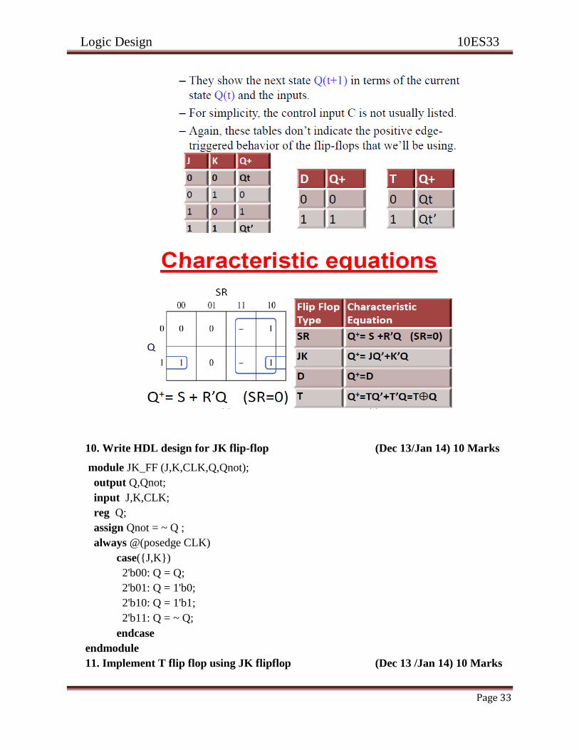
10. Write HDL design for JK flip-flop (Dec 13/Jan 14) 10 Marks
module JK_FF (J,K,CLK,Q,Qnot);
output Q,Qnot;
input J,K,CLK;
reg Q;
assign Qnot = ~ Q ;
always @(posedge CLK)
case({J,K})
2'b00: Q = Q;
2'b01: Q = 1'b0;
2'b10: Q = 1'b1;
2'b11: Q = ~ Q;
endcase
endmodule
11. Implement T flip flop using JK flipflop (Dec 13 /Jan 14) 10 Marks

Logic Design 10ES33
Page 34
12.Explain a 4 bit universal shift register in detail and give its timing diagram.
(Dec13 / Jan 14) 10 Marks
13.With neat timing diagram, explain the working of a 4-bit SISO register.

Logic Design 10ES33
Page 35
(Dec13 / Jan 14) 10 Marks
The serial in/serial out shift register accepts data serially--that is, one bit at a time on a single
line. It produces the stored information on its output also in serial form. With four stages, this
register can store up to four bits of data; its-storage capacity is four bits.
14.Design a 3 bit PISO(DFlip flop) (July 13)6 marks
Parallel-in to Serial-out (PISO) Shift Register
The Parallel-in to Serial-out shift register acts in the opposite way to the serial-in to parallel-out
one above. The data is loaded into the register in a parallel format in which all the data bits enter
their inputs simultaneously, to the parallel input pins PA to PD of the register. The data is then
read out sequentially in the normal shift-right mode from the register at Q representing the data
present at PAto PD.
This data is outputted one bit at a time on each clock cycle in a serial format. It is important to
note that with this system a clock pulse is not required to parallel load the register as it is already
present, but four clock pulses are required to unload the data.
4-bit Parallel-in to Serial-out Shift Register

Logic Design 10ES33
Page 36
15. Design two 4 bit serial adder. (July 13) 6marks
16. Design a 4 bit Johnson counters with sate table. (July 13)8 marks
4-bit Ring Counter
Truth Table for a 4-bit Johnson Ring Counter
Clock Pulse No FFA FFB FFC FFD
0 0 0 0 0
1 1 0 0 0
2 1 1 0 0
3 1 1 1 0

Logic Design 10ES33
Page 37
4 1 1 1 1
5 0 1 1 1
6 0 0 1 1
7 0 0 0 1
17.Explain Johnson Counter with neat diagram and timing diagram
(Dec13 / Jan 14) 10 Marks
The switch-tail ring counter, also know as the Johnson counter, overcomes some of the
limitations of the ring counter. Like a ring counter a Johnson counter is a shift register fed back
on its' self. It requires half the stages of a comparable ring counter for a given division ratio. If
the complement output of a ring counter is fed back to the input instead of the true output, a
Johnson counter results. The difference between a ring counter and a Johnson counter is which
output of the last stage is fed back (Q or Q'). Carefully compare the feedback connection below
to the previous ring counter.

Logic Design 10ES33
Page 38
18.Write verilog code for Shift Register. (July14) 10 Marks
module shftreg (s1,s0,Pin,lfin,rtin,A,CLK,Clr);
input s1,s0; //Select inputs
input lfin, rtin; //Serial inputs
input CLK,Clr; //Clock and Clear
input [3:0] Pin; //Parallel input
output [3:0] A; //Register output
reg [3:0] A;
always @ (posedge CLK or negedge Clr)
if (~Clr) A = 4'b0000;
else
case ({s1,s0})
2'b00: A = A; //No change
2'b01: A = {rtin,A[3:1]}; //Shift right
2'b10: A = {A[2:0],lfin}; //Shift left
//Parallel load input
2'b11: A = Pin;
endcase
endmodule
19.Give applications of J-K flip-flops. (July14) 4 Marks
J-K flip-flops are used in shift registers.
2. J-K flip-flops are used in counters.
Logic Design 10ES33
Page 39
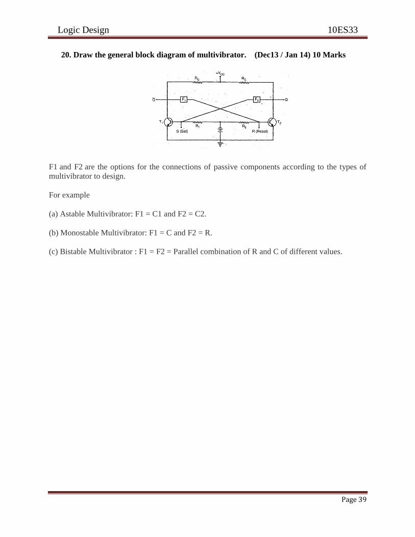
20. Draw the general block diagram of multivibrator. (Dec13 / Jan 14) 10 Marks
F1 and F2 are the options for the connections of passive components according to the types of
multivibrator to design.
For example
(a) Astable Multivibrator: F1 = C1 and F2 = C2.
(b) Monostable Multivibrator: F1 = C and F2 = R.
(c) Bistable Multivibrator : F1 = F2 = Parallel combination of R and C of different values.
Logic Design 10ES33
Page 40
Unit-6
Sequential Circuits – 2
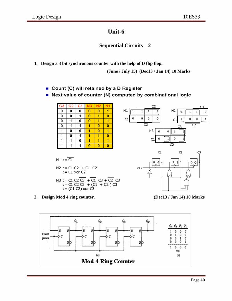
1. Design a 3 bit synchronous counter with the help of D flip flop.
(June / July 15) (Dec13 / Jan 14) 10 Marks
2. Design Mod 4 ring counter. (Dec13 / Jan 14) 10 Marks

Logic Design 10ES33
Page 41
The output of LSB FF is connected as D input to MSB FF.
This is commonly called as Ring Counter or Circular Counter.
The data is shifted to right with each clock pulse.
This counter has four different states.
This can be extended to any no. of bits.
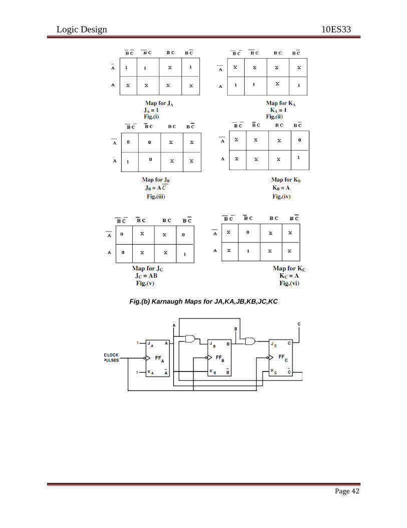
3. Design a synchronous mod 6 up counter using JKflip flop (July 13) 10 Marks.
Design of Mod-6 Counter: To design the Mod-6 synchronous counter, contain six counter
states (that is, from 0 to 6). For this counter, the counter design table lists the three flip-flop and
their states as 0 to 6 and the 6 inputs for the 3 flip-flops. The flip-flop inputs essential to step up
the counter from the now to the next state is worked out along with the help of the excitation
table. The needed counter states and the J K inputs essential for counter flip- flops are specified
in the counter design table demonstrated in Table no.1.
Input pulse
count
Counter States Flip-Flop Inputs
A B C JA KA JB KB JC KC
0 0 0 0 1 X 0 X 0 X
1 1 0 0 X 1 1 X 0 X
2 0 1 0 1 X X 0 0 X
3 1 1 0 X 1 X 1 1 X
4 0 0 1 1 X 0 X X 0
5 1 0 1 X 1 0 X X 1
6(0) 0 0 0
Logic Design 10ES33
Page 42
Fig.(b) Karnaugh Maps for JA,KA,JB,KB,JC,KC

Logic Design 10ES33
Page 43
4. Explain Digital clock with block Diagram. (July 13) 10 Marks
5. Design Mod 8 Johnson Counter. (June 13) 10 Marks

Logic Design 10ES33
Page 44
6. Difference between Asynchronous and Synchronous Counter.
(Dec14 / Jan 15) 10 Marks
Asynchronous Counter Synchronous Counter
1. Clock input is applied to LSB FF. The output
of first FF is connected as clock to next FF.
1. Clock input is common to all FF.
2. All Flip-Flops are toggle FF. 2. Any FF can be used.
3. Speed depends on no. of FF used for n bit . 3. Speed is independent of no. of FF used.
4. No extra Logic Gates are required. 4. Logic Gates are required based on
design.
5. Cost is less. 5. Cost is more.
7. Draw logic circuit diagram for 3-bit synchronous up-down counter with clear input,
start input and ‘done’ output. The counter should produce ‘done’ output after
completion of counter in either direction. (July 2014.) 10 Marks
8. Draw the logic circuits and the excitation tables for the T, JK flip-flops.
(Dec14 / Jan 15) 10 Marks
Logic Design 10ES33
Page 45
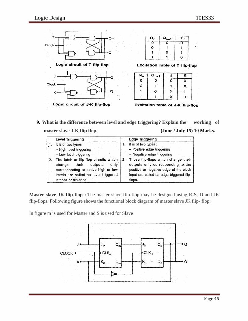
9. What is the difference between level and edge triggering? Explain the working of
master slave J-K flip flop. (June / July 15) 10 Marks.
Master slave JK flip-flop : The master slave flip-flop may be designed using R-S, D and JK
flip-flops. Following figure shows the functional block diagram of master slave JK flip- flop:
In figure m is used for Master and S is used for Slave
Logic Design 10ES33
Page 46
Unit-7
Sequential Design- 1
1. Difference between Mealy Model and Moore Model of Synchronous Sequential
Circuit. (June / July 15) (Dec13 / Jan 14) 10 Marks
Mealy Model : In Mealy Model the next state is function of external inputs and present state.
The output is also function of external inputs and present state. The memory state changes with
master clock.
Q+ = f(X,Q) Z = g(X,Q)
Moore Model : In Moore Model the next state is function of external inputs and present state.
But the output is function of present state. It is not dependent on external inputs. The no. of FFs
required to implement circuit is more compared with Mealy Model,
Q+ = f(X,Q) Z = g(Q)
2.Explain about all the notation of state machine. (July 13 ) 10 Marks.
• Input Variables : External input variables to sequential machine as inputs.
• Output Variables : All variables that exit from the sequential machine are output
variables.
• State : State of sequential machine is defined by the content of memory, when memory is
realized by using FFs.
• Present State : The status of all state variable i.e. content of FF for given instant of time t
is called as present state.
• Next State : The state of memory at t+1 is called as Next state.
• State Diagram : State diagram is graphical representation of state variables represented by
circle. The connection between two states represented by lives with arrows and also
indicates the excitation input and related outputs.
• Output Variables : All variables that exit from the sequential machine are output
variables.

Logic Design 10ES33
Page 47
3. Analyses the following circuit. (June/July15)(July13)10Marks.
By substituting the FF inputs in characteristic equation, the next state of FF is obtained in terms
of PS of FF and external input.
The characteristic equation of JK FF is
PS
Q2 Q1
(y2 y1)
Excitation input
J2 K2 J1
K1
x=0, 1 x=0, 1
Output Z
x=0, x=1
0 0 0 1 0 1 1 1
0 1 0 1 0 1 0 0
1 0 0 1 1 0 1 1
1 1 0 1 1 0 2 0
PS NS O/p Z
x = 0 x = 1
212122
1212
, , , yKyJxKxJ
yxyyyxZ
QKQJQ
22222
211111
xQKQJQ
QQKQJQ
112
112222
221221
,1 ,0
, ,
,
yzxWhenandyyzxWhen
yxyyyxZxKxJ
QyKQyJ

Logic Design 10ES33
Page 48
Q2
(y2)
Q1
(y1)
state Q2+ Q1+ state Q2+ Q1+ state X=0 X=1
0 0 A 0 0 A 1 0 C 1 1
0 1 B 0 0 A 1 0 C 0 0
1 0 C 0 1 B 1 1 D 1 1
1 1 D 0 1 B 1 1 D 1 0
State Diagram of Mealy Network
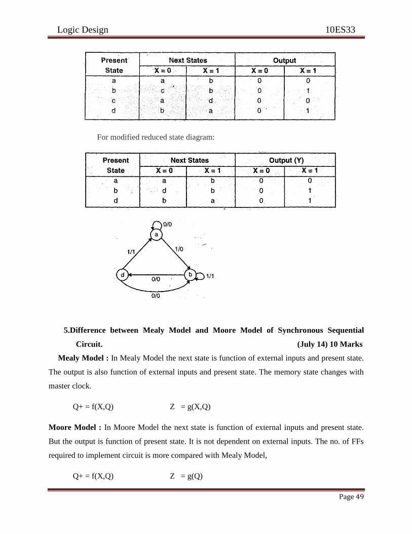
4.For the given state diagram, draw the state reduction diagram.
(Dec14 / Jan 15) 10 Marks
Ans. State table is as shown:
A
D
C
B
0/1
0/0
0/1
1/0
1/1
0/1
1/1 1/0
Logic Design 10ES33
Page 49
For modified reduced state diagram:
5.Difference between Mealy Model and Moore Model of Synchronous Sequential
Circuit. (July 14) 10 Marks
Mealy Model : In Mealy Model the next state is function of external inputs and present state.
The output is also function of external inputs and present state. The memory state changes with
master clock.
Q+ = f(X,Q) Z = g(X,Q)
Moore Model : In Moore Model the next state is function of external inputs and present state.
But the output is function of present state. It is not dependent on external inputs. The no. of FFs
required to implement circuit is more compared with Mealy Model,
Q+ = f(X,Q) Z = g(Q)

Logic Design 10ES33
Page 50
6. Analyses the following circuit. (Dec14 / Jan 15) 10 Marks.
State Table / Transition Table
PS NS O/p Z
x = 0 x = 1
Q1 Q2 State Q1+ Q2+ State Q1+ Q2+ state
0 0 A 0 0 A 0 1 B 0
0 1 B 1 1 D 0 0 A 1
1 0 C 0 0 A 0 0 A 1
1 1 D 1 0 C 0 0 A 1
2121
12221
21
2112221
Q & 0,1
Q & ,0
,
QDDxif
QDQDxif
QQZ
QQxQQxDQxD

Logic Design 10ES33
Page 51
State Diagram of Moore Network
D
1
0
B
1
C
1
A
0 1
0
0
0
0 1
1
Logic Design 10ES33
Page 52
Unit -8
Sequential Design- 2
1. Give performance parameters of DAC or D/A converters.
(June / July 15) (Dec13 / Jan 14) 10 Marks
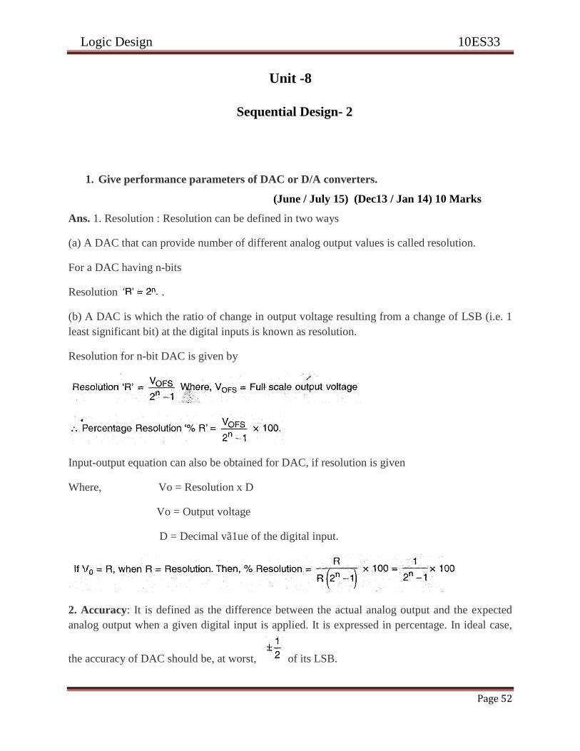
Ans. 1. Resolution : Resolution can be defined in two ways
(a) A DAC that can provide number of different analog output values is called resolution.
For a DAC having n-bits
Resolution .
(b) A DAC is which the ratio of change in output voltage resulting from a change of LSB (i.e. 1
least significant bit) at the digital inputs is known as resolution.
Resolution for n-bit DAC is given by
Input-output equation can also be obtained for DAC, if resolution is given
Where, Vo = Resolution x D
Vo = Output voltage
D = Decimal vã1ue of the digital input.
2. Accuracy: It is defined as the difference between the actual analog output and the expected
analog output when a given digital input is applied. It is expressed in percentage. In ideal case,
the accuracy of DAC should be, at worst, of its LSB.

Logic Design 10ES33
Page 53
3. Conversion Time or Setting Time: It is the time required for conversion of analog signal into
its digital equivalent. It is dependent on amplifiers output and switches response time.
4. Stability: When all the parameters such as gain, linearity error, monotonicity and offset must
be specified over the power supply ranges and full temperature then these parameters represent
the stability of the converter.
5. Monotonicity: If a converter does not miss any step backward during its entire range stepped
by a counter then it is said to have a counter having good monotonicity.
2. An 4 bit DIA converter has an output range of 0 to 1.5 V. Define its resolution.
(June / July 15) (Dec13 / Jan 14) 10 Marks
Ans. Give n = 4 = number of bits
Full scale output
1. Resolution:
Thus the output voltage can have 16 different values including zero.
2. Resolution:
Thus, an input change of 1 LSB changes the output by 100 mV.
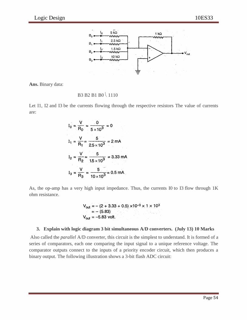
Following fig. shows the D1A converter with op-amp. Calculate the output if the input
digital signal is 1110. Assume 1 binary = +5V.
Logic Design 10ES33
Page 54
Ans. Binary data:
B3 B2 B1 B0 1110
Let I1, I2 and I3 be the currents flowing through the respective resistors The value of currents
are:
As, the op-amp has a very high input impedance. Thus, the currents I0 to I3 flow through 1K
ohm resistance.
3. Explain with logic diagram 3 bit simultaneous A/D converters. (July 13) 10 Marks
Also called the parallel A/D converter, this circuit is the simplest to understand. It is formed of a
series of comparators, each one comparing the input signal to a unique reference voltage. The
comparator outputs connect to the inputs of a priority encoder circuit, which then produces a
binary output. The following illustration shows a 3-bit flash ADC circuit:
Logic Design 10ES33
Page 55
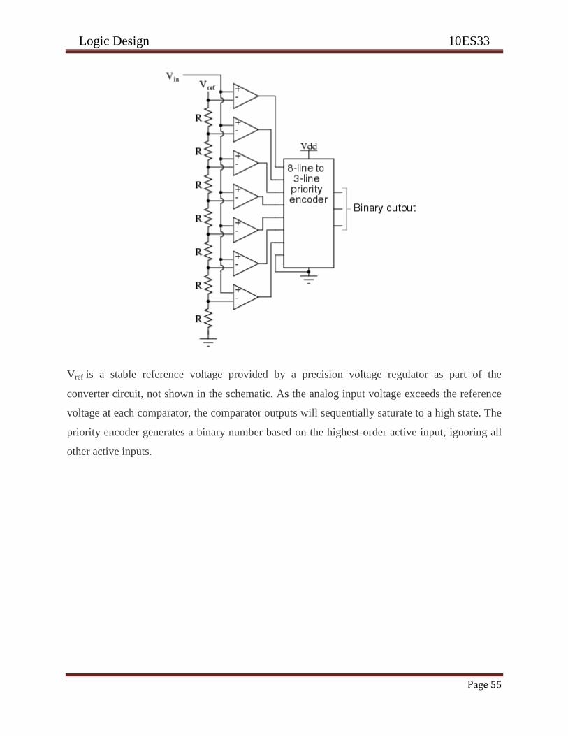
Vref is a stable reference voltage provided by a precision voltage regulator as part of the
converter circuit, not shown in the schematic. As the analog input voltage exceeds the reference
voltage at each comparator, the comparator outputs will sequentially saturate to a high state. The
priority encoder generates a binary number based on the highest-order active input, ignoring all
other active inputs.

Logic Design 10ES33
Page 56
4. Explain with logic diagram Single-slope A/D converters ( July 13) 10 Marks
Consider the circuit of Figure 14.1. As the op-amp’s non-inverting input, V+, istied to
ground, by making use of the golden rules we find that there is a virtual ground at the
inverting input. As long as the circuit’s input is connected to Vref, the current in the
resistor is Vref/R. This being the case the charge on the capacitor is increasing linearly.
Assuming that the charge on the capacitor is initially zero, the voltage on the capacitor is

Logic Design 10ES33
Page 57
5. Comment on the parameters which serve to describe the quality of performance of a
D/A converter. (Dec14 / Jan 15) 10 Marks
Ans. There are basic three parameters which describe the quality of performance of D/A
converter.
1. Resolution : It is the smallest possible change in the analog output voltage. Resolution should
be as high as possible.
2. Accuracy: It indicates how close the analog output voltage is to its theoretical value it is the
deviation of actual output from the theoretical value.
3. Linearity : The relation between the digital input and analog output should be linear.
6. With the help of a neat diagram explain parallel A/D converter.
(Dec14 / Jan 15) 10 Marks
Ans. Parallel A/D is used is much more due to its high speed. The only disadvantage is that its
hardware (no. of comparators) increase with the no. of bits. Va is analog, voltage and VR is
reference’ voltage.
A 3-bit parallel-comparator AID converter is shown in fig. Va is the analog voltage is be
converted into digital form. The voltage corresponding to full scale is V from which the
reference voltages VR1, VR2…. (See Fig.) are generated using the resistor network. The voltage
Va is

Logic Design 10ES33
Page 58
7. Explain the operation of successive approximation type of ADC (July 14 ) 10 Marks
Ans. Successive approximation is one of the most widely used popular method due its
efficiency The block diagram of SAR ADC s as shown:
Working: Initially, let us set the MSB bit of SAR register i.e. d1 = 1. It is applied to 4-bit D to A
converter i.e. as 1000. The D/A converter will generate its analog value and send to control logic
The output of control logic is VR. Now at the comparator, there are two inputs VR (Reference
voltage) and VA (Input analog).
If VR > VA output of comparator is low and bit d1 is reset correspondingly.
If VR <VA output of comparator is high and bit d1 remains high.
The same procedure is repeated for all bits i e for d2, d3,…. dn, and output may be taken in serial
or parallel manner.
Advantage: The conversion time is fixed as it does not depend upon amplitude of analog input.
8. An 8-bit successive approximation converter (SAC) has a resolution of 15 mV What
will its, digital output be for an analog input of 2.65 V? (July 14) 10 Marks
Ans. Analog input = 2.65 V
Resolution = 15 mV
Now 176 would produce 2.64 V and 177 would produce 2.65 V. Hence VA = 2.65V The digital
result will be (176)10 = (10110000)2
Logic Design 10ES33
Page 59
9. Define linearity, settling time, sensitivity and accuracy of A/D and D/A converters.
(Dec14 / Jan 15) 8 Marks
Ans. For D/A converters
Linearity: The linearity of the converter specifies the accuracy with which the ideal
performance is followed Output of DIA converter must be each step up (down) in the digital
input so as to cause an increase (decrease) in the analog output The linearity should be at least
equal to or better then
(ii) Setting Time: Whenever a digital input is applied to D/A converter, sometimes output sets to
a value within some specific limit of the final value The limit range is
LSB or less. This parameter tells the speed of D/A converter and t can be calculated by use
o switches, amplifier, resistors etc. in the device.
i. Accuracy: It is a measure of the difference between actual output and expected output. It is
given as a percentage of the maximum output voltage. If the maximum output voltage i.e. full
scale deflection is 5V and accuracy is then, the maximum error is x 5 = 0.0005 V
or 5mV. Ideally the accuracy should be better than 0.5 of LSB.
In an 8-bit converter LSB is or 0.39% of full scale. The accuracy should be better
than 0.2%.
(iv) Sensitivity : Due to change in temperature the output of D/A converter should not change.
But practically the value of resistances and operational amplifier parameters change with
variation in temperature as analog output is a function of temperature. For AID converters
(i) Linearity: Linearity is basically a ‘best straight line’. Linearity of a converter directly
determines the relative accuracy of the converter. It is the difference of errors betweens the
nominal and actual ratios to the full scale analog value corresponding to a
given digital input and independent of full scale calibration. The linearity error should be less
than
(ii) Conversion Time or Setting Time : It is the -time refers to the time requires for a complete
measurement by analog to digital converter.
OR

Logic Design 10ES33
Page 60
It is the time required for conversion of analog signal into its digital equivalent. It is dependent
on the amplifiers output and switches response time.
(iii) Accuracy : The accuracy of a given ADC i.e. analog to digital converter determines the
number of bits which can be usefully provided.
The accuracy of an ADC consists of quantization error system noise etc. Typical values are
0.02% of the full scale reading.
(iv) Sensitivity : Due to change in temperature the output of AID converter should not change.
But the value of resistances and operational amplifier change with change in temperature.
10. Write note on the following Binary ladder D/A. converter (Dec13 / Jan 14) 6 Marks
Ans Binary ladder D/A converter In a binary ladder D/A converter only two valued resistance
R and 2R are used as shown in diagram
The OP amp is an inverting amplifier By solving resistance N/W in parallel and series, finally
voltage at node B is.

Logic Design 10ES33
Page 61
11. Explain the operation of dual-slope A/D converter. (Dec13 / Jan 14) 8 Marks
Ans. The dual slop A/D converter provide very much accuracy and so mostly used.
An analog input voltage is applied to Ramp Generator. The output of Ramp Generator app1ied to
comparator. The output of comparator is given to ‘AND’ gate. The second output ‘AND’ gate is
clock pulse. When input is high for AND gate clock pulse will be given to m-r. Counter is
initially reset by control logic. Now counter counts up and binary output in form is provided.
When counter stops, switch control again control the whole function.