
Two Dimensional Gauge Theories and Quantum Integrable Systems

QUANTUM TRANSPORT IN ONE-DIMENSIONAL
NANOSTRUCTURES
A DISSERTATION
SUBMITTED TO THE DEPARTMENT OF PHYSICS
AND THE COMMITTEE ON GRADUATE STUDIES
OF STANFORD UNIVERSITY
IN PARTIAL FULFILLMENT OF THE REQUIREMENTS
FOR THE DEGREE OF
DOCTOR OF PHILOSOPHY
Joseph A. Sulpizio
May 2011

http://creativecommons.org/licenses/by-nc/3.0/us/
This dissertation is online at: http://purl.stanford.edu/zc523gt0725
© 2011 by Joseph Albert Sulpizio. All Rights Reserved.
Re-distributed by Stanford University under license with the author.
This work is licensed under a Creative Commons Attribution-Noncommercial 3.0 United States License.
ii

I certify that I have read this dissertation and that, in my opinion, it is fully adequatein scope and quality as a dissertation for the degree of Doctor of Philosophy.
David Goldhaber-Gordon, Primary Adviser
I certify that I have read this dissertation and that, in my opinion, it is fully adequatein scope and quality as a dissertation for the degree of Doctor of Philosophy.
Daniel Fisher
I certify that I have read this dissertation and that, in my opinion, it is fully adequatein scope and quality as a dissertation for the degree of Doctor of Philosophy.
Harindran Manoharan
Approved for the Stanford University Committee on Graduate Studies.
Patricia J. Gumport, Vice Provost Graduate Education
This signature page was generated electronically upon submission of this dissertation in electronic format. An original signed hard copy of the signature page is on file inUniversity Archives.
iii

Abstract
One-dimensional (1D) nanostructures comprise a class of systems that boast tremen-
dous promise for both technological innovation as well as fundamental scientific dis-
covery. In this thesis, we describe our investigations down three avenues of quantum
transport in 1D: (1) ballistic transport in quantum wires, (2) quantum capacitance
measurements of nanostructures, and (3) tunneling measurements in carbon nan-
otubes.
First, we present measurements of hole transport in ballistic quantum wires fab-
ricated by GaAs/AlGaAs cleaved-edge overgrowth (CEO), as hole transport in GaAs
is expected to exhibit enhanced effects of electron-electron interactions and spin-orbit
coupling as compared with transport of electrons. To interpret these results, we have
developed a new, broadly-applicable approach to analyzing the transport measure-
ments of a ballistic 1D quantum system. We validate our analysis approach using
nonlinear conductance data of both electron and hole CEO quantum wires. Apply-
ing our analysis to measurements of hole transport in magnetic field, we find strong
g-factor anisotropy, which we associate with spin-orbit coupling, and evidence for
the importance of charge interactions, indicated by the observation of 0.7 structure.
Additionally, we present the first experimental observation of a predicted “spin-orbit
gap” in the 1D density of states, where counter-propagating spins constituting a spin
current are accompanied by a clear signal in the conductance.
Next, we discuss our development of a highly sensitive integrated capacitance
bridge for quantum capacitance measurements. Such measurements serve as a novel
probe of 1D systems, and are not subject to many of the limitations of conventional
transport measurements. Our bridge, based on a GaAs HEMT amplifier, delivers
iv
attofarad (aF) resolution using a small AC excitation at or below kBT over a broad
temperature range (4K-300K). We have achieved a resolution at room temperature
of 60aF/√Hz for a 10mV AC excitation at 17.5 kHz, with improved resolution at
cryogenic temperatures for the same excitation amplitude. We demonstrate the utility
of our bridge by measuring the capacitance of top-gated graphene devices, where
we cleanly resolve the density of states. We also present preliminary capacitance
measurements of carbon nanotube devices, where we ultimately aim to extract their
mobility.
Finally, we discuss how interacting systems of fermions in 1D are fundamentally
different from higher dimensional systems, and propose a set of tunneling measure-
ments in carbon nanotubes to probe these interactions in which narrow top gates are
used to introduce tunable barriers. We explore two top-gated nanotube transistor
fabrication schemes, one employing global alignment and the other local alignment,
and present initial transport measurements that highlight the technological barriers
currently impeding these studies.
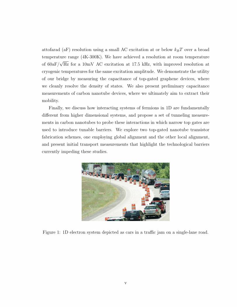
Figure 1: 1D electron system depicted as cars in a traffic jam on a single-lane road.
v

Epigraph
Tout existant naıt sans raison, se prolonge par faiblesse et meurt par ren-
contre.
–Jean-Paul Sartre, La Nausee.
vi

Acknowledgements
I once stated that my advisor, David Goldhaber-Gordon was “the world’s greatest
human.” While this is likely an overstatement to some extent, it speaks to both
his tremendous scientific abilities and his character. David has fostered a vibrant,
collegial lab culture, where students are granted the freedom to develop their own
scientific ideas, and I am deeply thankful to have been fortunate enough to be a part
of such an amazing group.
I’d also like to express my gratitude to the other members of my defense commit-
tee: Hari Manoharan, Daniel Fisher, Xiao-Liang Qi, and Yi Cui.
At the beginning of my PhD, I had the opportunity to be an intern at Hitachi
Global Storage Technologies (formerly IBM) working directly with the amazingly tal-
ented Zvonimir Bandic, who is a wealth of physics and materials knowledge. This was
my first real foray into nanofabrication, and it developed into a lasting collaboration
with Zvonimir for which I am grateful.
The CEO research was performed in close collaboration with Charis Quay, who
preceded me in the DGG lab. Over the years, Charis taught me a tremendous amount
of mesoscopic physics, both theoretical and experimental, and I hope we can work
together again in the future. It has also been great interacting with Rafi de Picciotto,
whose expertise and physical insight I’ve greatly enjoyed through our numerous dis-
cussions. Of course, none of the CEO work would have been possible without the
MBE prowess exuded by Loren Pfeiffer, Ken West, and Kirk Baldwin. Thanks also
to Taylor Hughes for expertly providing theoretical support for all of the spin-orbit
coupling work, and to Tomaz Rejec for performing DFT simulations.
The quantum capacitance work was done in collaboration with H.-S. Philip Wong’s
vii

group in the electrical engineering department, and I worked closely with his student,
Arash Hazeghi. It was a great experience to gain an engineering-oriented research
perspective (quite different from the outlook of a physicist), and to learn about de-
vices/circuits from such experts. Thanks are also due to Ray Ashoori, Stuart Tessmer,
and Gary Steele for many helpful discussions regarding their pioneering work in the
field, and to James Harris and Shahal Ilani for crucial measurement advice. I also
thank Yi-Ching Pao and Diana Fong for help with substrate preparation and tricky
wirebonding, and Jeff Bokor and Patrick Bennett for use of equipment.
Thanks also to Peter Burke and Wei Wei Zhou at UCI for providing the ultra-long
nanotubes used in the fabrication of top-gated nanotube devices.
Not mentioned in this thesis is research I performed on transport across poten-
tial barriers in graphene. Thanks to the labmates involved, this was a fantastically
productive diversion from my 1D research. Yang Bo, Nimrod Stander, and Benjamin
Huard comprised a driven team of gifted researchers, and I am really thankful to have
learned so much working with them during such an exciting period.
I’d also like to thank the other DGG group members with whom I’ve had the plea-
sure of sharing the lab over the years, for countless discussions, scientific and other-
wise, and for tolerating my music: Lindsay Moore, Hungtao Chou, Mike Jura, Ron Po-
tok, Mark Topinka, Mike Grobis, John Cumings, Ileana Rau, Sami Amasha, Kathryn
Todd, Markus Konig, Matthias Baenninger, Patrick Gallagher, Jimmy Williams,
Menyoung Lee, Andrew Keller, Andrew Bestwick, Michael Neumann, Georgy Di-
ankov, Matthew Pelliccione, and Francois Amet. In particular, I thank Alex Neuhausen,
Adam Sciambi, and Andrei Garcia for their eagerness to engage in science, their ex-
traordinary talents inside the lab, and continuing friendship beyond.
The collaborative nature of the labs in GLAM, where the DGG group is housed,
has given me the benefit of learning from a number of nearby scientists (and has also
given me access to their tools/equipment). I’d like to thank Kam Moler’s group (es-
pecially Ophir Auslaender for many helpful discussions), Aharon Kapitulnik’s Group,
Nick Melosh’s group (especially Mike Preiner and Piyush Verma for sharing the SEM
maintenance duties), Yi Cui’s group, and Mark Brongersma’s Group (especially Ed
Barnard for assistance with the Raman microscope). I also thank the administrators
viii

and support staff, especially Mark Gibson and Maria Frank, for helping navigate the
Stanford bureaucracy.
Additionally, I thank the generous financial support from our funding agencies,
primarily the AFOSR and the NSF.
Finally, and most importantly, I thank my family and all my friends from Stanford
and beyond for their continued love and support. It has certainly been an interesting
journey.
ix

Contents
Abstract iv
Epigraph vi
Acknowledgements vii
1 Introduction 1
1.1 Motivation . . . . . . . . . . . . . . . . . . . . . . . . . . . . . . . . . 1
1.2 Overview of Quantum Transport . . . . . . . . . . . . . . . . . . . . 1
1.2.1 Bulk Transport . . . . . . . . . . . . . . . . . . . . . . . . . . 2
1.2.2 Ballistic Transport . . . . . . . . . . . . . . . . . . . . . . . . 4
1.2.3 The 1D Limit . . . . . . . . . . . . . . . . . . . . . . . . . . . 6
1.3 Overview of Thesis . . . . . . . . . . . . . . . . . . . . . . . . . . . . 7
2 Cleaved-Edge Overgrowth Quantum Wires 9
2.1 Introduction . . . . . . . . . . . . . . . . . . . . . . . . . . . . . . . . 9
2.2 Fabrication and Operation of CEO Quantum Wires . . . . . . . . . . 10
2.2.1 CEO Wire Fabrication . . . . . . . . . . . . . . . . . . . . . . 10
2.2.2 Operation of CEO Quantum Wires . . . . . . . . . . . . . . . 11
2.3 Previous Studies on CEO Electron Wires . . . . . . . . . . . . . . . . 15
2.4 Ballistic Transport in 1D . . . . . . . . . . . . . . . . . . . . . . . . . 17
2.4.1 1D Subband Coupled to a Gate . . . . . . . . . . . . . . . . . 18
2.4.2 Ballistic Transport Model at Non-zero Source-Drain Bias . . . 21
2.4.3 Introduction to Nonlinear Transport Measurements . . . . . . 22
x

2.4.4 Nonlinear Transport in CEO Electron Wires . . . . . . . . . . 24
2.4.5 Fitting the Model to the Data at the First Diamond . . . . . . 29
2.4.6 Fitting the Model to the Data at Higher Diamonds . . . . . . 30
2.4.7 Gate Coupling and Multiple Subbands . . . . . . . . . . . . . 34
2.4.8 DFT Modeling of CEO Wires . . . . . . . . . . . . . . . . . . 37
2.5 Nonlinear Transport in CEO Hole Wires . . . . . . . . . . . . . . . . 39
2.5.1 Data Filtering . . . . . . . . . . . . . . . . . . . . . . . . . . . 39
2.5.2 Series Resistance Removal and Feature Extraction . . . . . . . 40
2.5.3 Model Fitting . . . . . . . . . . . . . . . . . . . . . . . . . . . 42
2.5.4 Hole wire transconductance discussion . . . . . . . . . . . . . 44
2.6 g-factor measurements . . . . . . . . . . . . . . . . . . . . . . . . . . 46
2.6.1 Qualitative discussion of 1D magnetotransport . . . . . . . . . 47
2.6.2 Zeeman splitting in CEO Hole Wires . . . . . . . . . . . . . . 48
2.7 0.7 Structure in CEO Hole Wires . . . . . . . . . . . . . . . . . . . . 51
2.7.1 Hole wire degeneracy . . . . . . . . . . . . . . . . . . . . . . . 53
2.8 Spin-Orbit Coupling in 1D . . . . . . . . . . . . . . . . . . . . . . . . 54
2.8.1 Overview of Spin-Orbit Coupling . . . . . . . . . . . . . . . . 55
2.8.2 Experimental observation of spin-orbit gap . . . . . . . . . . . 58
2.8.3 Modeling of spin-orbit gap dispersions . . . . . . . . . . . . . 62
2.8.4 Modeled 1D spin-orbit dispersions and conductance simulations 67
2.9 Future Directions . . . . . . . . . . . . . . . . . . . . . . . . . . . . . 70
3 Quantum Capacitance 72
3.1 Introduction . . . . . . . . . . . . . . . . . . . . . . . . . . . . . . . . 72
3.2 Fundamentals of Quantum Capacitance . . . . . . . . . . . . . . . . . 73
3.2.1 Quantum Capacitance with Multiple Gates . . . . . . . . . . . 78
3.2.2 Screening . . . . . . . . . . . . . . . . . . . . . . . . . . . . . 81
3.3 Applications of Quantum Capacitance and Proposed Measurements . 83
3.4 Quantum Capacitance Measurement Techniques and Challenges . . . 86
3.5 The Integrated Capacitance Bridge . . . . . . . . . . . . . . . . . . . 88
3.5.1 Amplifier and Bridge Circuit Design . . . . . . . . . . . . . . 89
xi

3.5.2 Substrate Fabrication and Circuit Mounting . . . . . . . . . . 91
3.5.3 Bridge Circuit Operation and Optimization . . . . . . . . . . 93
3.5.4 Measurement Noise . . . . . . . . . . . . . . . . . . . . . . . . 97
3.5.5 Characterizing Bridge Performance: Graphene Quantum Ca-
pacitance Measurements . . . . . . . . . . . . . . . . . . . . . 98
3.5.6 Summary of the Integrated Capacitance Bridge . . . . . . . . 104
3.6 Future Directions . . . . . . . . . . . . . . . . . . . . . . . . . . . . . 104
4 Transport Across Tunnel Barriers in 1D 107
4.1 Introduction . . . . . . . . . . . . . . . . . . . . . . . . . . . . . . . . 107
4.2 The Failure of Fermi Liquid Theory in 1D . . . . . . . . . . . . . . . 107
4.2.1 Luttinger Liquids . . . . . . . . . . . . . . . . . . . . . . . . . 110
4.3 Probing Interactions in 1D: Tunneling . . . . . . . . . . . . . . . . . 112
4.3.1 Tunneling Across Barriers in Carbon Nanotubes . . . . . . . . 113
4.4 Device Fabrication . . . . . . . . . . . . . . . . . . . . . . . . . . . . 114
4.4.1 Global Alignment . . . . . . . . . . . . . . . . . . . . . . . . . 114
4.4.2 Local Alignment . . . . . . . . . . . . . . . . . . . . . . . . . 118
4.5 Device Phenomenology and Limitations . . . . . . . . . . . . . . . . . 119
4.5.1 Fabry-Perot Regime . . . . . . . . . . . . . . . . . . . . . . . 121
4.5.2 Coulomb Blockade Regime . . . . . . . . . . . . . . . . . . . . 121
4.5.3 Transition Regime . . . . . . . . . . . . . . . . . . . . . . . . 123
4.6 Future Directions . . . . . . . . . . . . . . . . . . . . . . . . . . . . . 125
A CEO Wire Measurements 127
A.1 Measurement Circuit and Setup . . . . . . . . . . . . . . . . . . . . . 127
A.2 Measurement and Sample Details . . . . . . . . . . . . . . . . . . . . 128
B Carbon Nanotube Growth and Characterization 129
B.1 Growth . . . . . . . . . . . . . . . . . . . . . . . . . . . . . . . . . . 129
B.2 AFM Characterization . . . . . . . . . . . . . . . . . . . . . . . . . . 130
xii

C Measurement Schemes and Code 132
C.1 Overview of High-Level Measurement Programs . . . . . . . . . . . . 132
C.1.1 Conductance Measurements . . . . . . . . . . . . . . . . . . . 132
C.1.2 Capacitance Measurements . . . . . . . . . . . . . . . . . . . . 134
C.2 List of Low-Level Instrument Control Functions . . . . . . . . . . . . 135
D Simulation and Analysis Code 137
D.1 Capacitance Simulations . . . . . . . . . . . . . . . . . . . . . . . . . 137
D.1.1 Graphene Quantum Capacitance . . . . . . . . . . . . . . . . 138
D.2 1D Ballistic Conductance Simulations . . . . . . . . . . . . . . . . . . 139
D.2.1 CEO Quantum Hole Wire Conductance . . . . . . . . . . . . . 140
Bibliography 142
xiii

List of Tables
2.1 Parameters used in DFT simulation of quantum wires. . . . . . . . . 37
2.2 Values of CEO hole wire parameters used in degeneracy calculation . 54
2.3 Parameters and values used in 1D spin-orbit model . . . . . . . . . . 66
3.1 Optimized HEMT bias conditions with corresponding amplifier output
sensitivity S and best achievable capacitance resolution δC (per root
Hz) . . . . . . . . . . . . . . . . . . . . . . . . . . . . . . . . . . . . . 93
xiv

List of Figures
1 1D electron system depicted as cars in a traffic jam on a single-lane road v
1.1 Artists’ renditions of 1D circuits . . . . . . . . . . . . . . . . . . . . . 2
1.2 Transport in a bulk, ohmic system . . . . . . . . . . . . . . . . . . . 3
1.3 Transport in the quantum, ballistic regime . . . . . . . . . . . . . . . 4
1.4 The 1D limit of a nanostructure . . . . . . . . . . . . . . . . . . . . . 6
1.5 Quantized conductance in quantum point contacts . . . . . . . . . . . 7
2.1 Fabrication of CEO quantum wires . . . . . . . . . . . . . . . . . . . 12
2.2 Images of CEO quantum wire chips . . . . . . . . . . . . . . . . . . . 13
2.3 Schematic overview of CEO quantum wire operation . . . . . . . . . 14
2.4 Conductance quantization in CEO quantum wires . . . . . . . . . . . 15
2.5 Previous studies of CEO electron wires . . . . . . . . . . . . . . . . . 16
2.6 Simplified schematic of 1D channel . . . . . . . . . . . . . . . . . . . 17
2.7 Physical interpretation of (2.6) . . . . . . . . . . . . . . . . . . . . . 19
2.8 Single-particle electrostatic derivation of (2.6) . . . . . . . . . . . . . 20
2.9 1D channel at non-zero source-drain bias . . . . . . . . . . . . . . . . 22
2.10 Schematic overview of nonlinear transport data . . . . . . . . . . . . 23
2.11 Transconductance∣∣∣ ∂G∂Vg
∣∣∣ map of CEO electron wire . . . . . . . . . . . 25
2.12 Fixed populations of right-movers or left-movers along a conductance
transition . . . . . . . . . . . . . . . . . . . . . . . . . . . . . . . . . 27
2.13 Transconductance map with positions of zero-bias vertices and sub-
band spacings overlaid . . . . . . . . . . . . . . . . . . . . . . . . . . 29
xv

2.14 Conductance transition curves for the first “diamond” (lowest energy
set of transition curves) superimposed on the transconductance map . 30
2.15 Conductance transition curves for upper diamonds superimposed on
the transconductance map using a fixed value for the geometric capac-
itance . . . . . . . . . . . . . . . . . . . . . . . . . . . . . . . . . . . 31
2.16 Generated transition curves with continuously varying geometric ca-
pacitance superimposed on transconductance map . . . . . . . . . . . 33
2.17 Geometric capacitance versus gate voltage extracted from equations
(2.23) and (2.19) . . . . . . . . . . . . . . . . . . . . . . . . . . . . . 34
2.18 Schematic for model where individual subbands are treated as capaci-
tively coupled wires . . . . . . . . . . . . . . . . . . . . . . . . . . . . 35
2.19 DFT simulations of a CEO quantum wire . . . . . . . . . . . . . . . . 38
2.20 Numerical solution to subband density for derived wire model . . . . 39
2.21 Transport data at various stages of processing . . . . . . . . . . . . . 40
2.22 Bias voltage correction illustrated at conductance transition for edge
of second subband . . . . . . . . . . . . . . . . . . . . . . . . . . . . 41
2.23 CEO Hole wire transconductance and corresponding fits to the con-
ductance transitions . . . . . . . . . . . . . . . . . . . . . . . . . . . 43
2.24 Nonlinear transport and conductance transition types in CEO hole wires 45
2.25 Influence of magnetic field on 1D subbands . . . . . . . . . . . . . . . 47
2.26 Magnetoconductance of CEO hole wires . . . . . . . . . . . . . . . . 49
2.27 Hole wire nonlinear transconductance in static 9T field oriented parallel
to axis of wire . . . . . . . . . . . . . . . . . . . . . . . . . . . . . . . 51
2.28 0.7 structure at the second hole wire subband . . . . . . . . . . . . . 52
2.29 Conductance features used in hole wire degeneracy calculation. . . . . 54
2.30 Spin-orbit coupling in a 1D subband . . . . . . . . . . . . . . . . . . 56
2.31 Spin-orbit coupling in a 1D subband with external magnetic field . . 57
2.32 Dispersions and associated conductance for multiple 1D subbands with
spin-orbit coupling with various configurations of external magnetic field 59
2.33 Observation of 1D spin-orbit gap . . . . . . . . . . . . . . . . . . . . 60
2.34 CEO hole wire data continuity and reproducibility . . . . . . . . . . . 61
xvi

2.35 2D GaAs dispersions from [97] . . . . . . . . . . . . . . . . . . . . . . 62
2.36 Calculated 1D Dispersions from Luttinger model and associated simu-
lated conductance traces . . . . . . . . . . . . . . . . . . . . . . . . . 68
3.1 Subband schematic for quantum capacitance . . . . . . . . . . . . . . 74
3.2 Equivalent circuit for the device shown in 3.1, which can be considered
a series combination of the gate capacitance and a “quantum capaci-
tance.” . . . . . . . . . . . . . . . . . . . . . . . . . . . . . . . . . . . 75
3.3 Capacitance per unit area of parallel-plate capacitor made from GaAs
2DEG as a function of gate-coupling (κ/d) . . . . . . . . . . . . . . . 77
3.4 Capacitive-coupling of multiple gates to a subband . . . . . . . . . . 79
3.5 Field-penetration quantum capacitance measurement geometry . . . . 81
3.6 Graphene nanoribbon DOS for zigzag ribbons of various widths in units
of carbon atoms N . . . . . . . . . . . . . . . . . . . . . . . . . . . . 84
3.7 Previous measurements of nanotube quantum capacitance and conduc-
tance evidence of transport through multiple subbands . . . . . . . . 85
3.8 Conventional impedance measurement circuitry . . . . . . . . . . . . 86
3.9 Parasitic cable capacitance in a typical capacitance test setup with a
CV meter . . . . . . . . . . . . . . . . . . . . . . . . . . . . . . . . . 87
3.10 Other quantum capacitance measurement schemes . . . . . . . . . . . 88
3.11 The integrated capacitance bridge operating principle . . . . . . . . . 89
3.12 Schematic of the integrated bridge circuit connected to a DUT . . . . 90
3.13 Output characteristics of Fujitsu FHX35X HEMT for Vgs = 0 at vari-
ous temperatures . . . . . . . . . . . . . . . . . . . . . . . . . . . . . 91
3.14 Substrate fabrication process flow for the integrated capacitance bridge 92
3.15 Noise performance of the integrated capacitance bridge . . . . . . . . 94
3.16 Schematic of integrated bridge measurement setup . . . . . . . . . . . 95
3.17 Integrated bridge output as a function of |νREF/νDUT | for different
temperatures and DUT excitations . . . . . . . . . . . . . . . . . . . 96
3.18 Images of integrated bridge circuit with attached graphene DUT . . . 99
xvii

3.19 Resistance of a graphene device versus back gate and top gate voltages
at room temperature . . . . . . . . . . . . . . . . . . . . . . . . . . . 100
3.20 CV curves for top-gated graphene device measured with the integrated
capacitance bridge . . . . . . . . . . . . . . . . . . . . . . . . . . . . 101
3.21 Comparison of measured CV curves for top-gated graphene device for
the AH2700A and the integrated bridge . . . . . . . . . . . . . . . . . 103
3.22 Photograph of top-gated nanotube device with capacitance bridge in
probestation and scanning electron micrograph of nanotube device . . 105
3.23 Preliminary capacitance data of an individual top-gated carbon nan-
otube measured via the integrated capacitance bridge . . . . . . . . . 106
4.1 Failure of Fermi liquid theory for 1D electron gas . . . . . . . . . . . 108
4.2 Particle-hole excitations in different dimensions . . . . . . . . . . . . 109
4.3 Bosonization of 1D fermions . . . . . . . . . . . . . . . . . . . . . . . 110
4.4 Transport through a Luttinger liquid and proposed measurement scheme112
4.5 Previous nanotube tunneling measurements . . . . . . . . . . . . . . 113
4.6 Process flow for global alignment fabrication of carbon nanotube top-
gated transistors . . . . . . . . . . . . . . . . . . . . . . . . . . . . . 115
4.7 Nanotube transistors fabricated using global alignment . . . . . . . . 116
4.8 Global alignment nanotube device transport . . . . . . . . . . . . . . 117
4.9 Nanotube device fabricated via local alignment methods . . . . . . . 118
4.10 Local gating in top-gated nanotubes at T=4K . . . . . . . . . . . . . 119
4.11 Conductance of nanotube device in various regimes: Fabry-Perot, Coulomb
blockade, and transition . . . . . . . . . . . . . . . . . . . . . . . . . 120
4.12 Coulomb blockade in a quantum dot . . . . . . . . . . . . . . . . . . 124
4.13 Nanotube devices from ultra-long growth . . . . . . . . . . . . . . . . 125
A.1 CEO hole wire measurement circuit and setup . . . . . . . . . . . . . 128
B.1 Scanning electron micrographs of grown carbon nanotubes . . . . . . 130
B.2 Atomic force microscope characterization of grown carbon nanotubes 131
C.1 Various conductance measurement schemes . . . . . . . . . . . . . . . 133
xviii

D.1 Simulated graphene carrier density and capacitance for various tem-
peratures . . . . . . . . . . . . . . . . . . . . . . . . . . . . . . . . . 138
D.2 Simulated dispersion (a), charge density (b) and conductance (c) for
a CEO quantum hole wire in magnetic field aligned along wire axis at
T =300mK . . . . . . . . . . . . . . . . . . . . . . . . . . . . . . . . 141
xix

Chapter 1
Introduction
1.1 Motivation
Advances in nanofabrication have led to the creation of one-dimensional (1D) nanos-
tructures, systems in which electrons are strongly confined in two spatial dimensions,
and comparatively free to propagate along the third dimension. Such systems hold
tremendous capacity for technological advancement, most notably with applications
for electronics as transistors and interconnects, as illustrated in figure 1.1. To fully
harness their potential, it is crucial to understand transport through 1D systems at
the most fundamental, quantum level. In this thesis, we aim to understand several
quantum transport phenomena through a series of transport measurements on various
1D nanostructures. In particular, we examine ballistic transport, spin-orbit coupling,
and electron-electron interactions, employing several measurement techniques.
1.2 Overview of Quantum Transport
The field of quantum transport is impressively broad, and it is thus impractical to give
an overview of all topics within a thesis. Instead, we provide a concise background of
relevant concepts which are expounded upon in the subsequent chapters. For a more
complete treatment, see the following references: [23, 22, 33].
1

CHAPTER 1. INTRODUCTION 2
Figure 1.1: Artists’ renditions of (rather fanciful) 1D circuits[7].
1.2.1 Bulk Transport
Electron transport through a bulk system is nicely described by Ohm’s law:
J = σE, (1.1)
where J is the current density, E is the applied electric field, and σ is the system’s
conductivity. The conductivity can then be explained through the familiar Drude
model[30]:
σ =e2nτmm⋆
, (1.2)
where m⋆ is the effective mass, n is the charge density, and τm is the average time
between momentum-relaxing scattering events for scatterers distributed with mean
free path separation Lm. Since current is carried by electrons at the Fermi level with

CHAPTER 1. INTRODUCTION 3
shi ed Fermi
surface
a) b)
Figure 1.2: Transport in a bulk, ohmic system. a) Metal connected to battery.Momentum-relaxing scattering sites are marked by x’s and are separated on averageby the mean-free path Lm. b) Diffusive transport through the metal from (a). Thechemical potential along the length of the metal changes linearly between the left andright contacts held at the potentials µL and µR, respectively. The equilibrium Fermilevel is marked by the dashed line. This system is equivalently described by a Fermisurface shifted from equilibrium by the momentum kd.
velocity νF , we have the simple relation:
Lm = νF τm. (1.3)
In reciprocal space, this model can be visualized as an equilibrium Fermi surface that
is shifted from the origin by a “drift” momentum kd given to each electron as a result
of the applied field:
kd =eτmE
ℏ. (1.4)
This is illustrated in figure 1.2.
An alternate view of transport, also illustrated in figure 1.2, invokes the diffusion
equation to describe electron flow:
J = −eD∇n, (1.5)

CHAPTER 1. INTRODUCTION 4
le-movers
right-movers
I
a) b)
Figure 1.3: Transport in the quantum, ballistic regime. a) A section of material oflength LS < Lm is contacted electrically. b) Current through this system is calculatedby explicitly considering the bandstructure, composed of a series of M 1D subbands.In the ballistic limit, with reflectionless contacts, transport through each 1D subbandis characterized by left-movers and right-movers, which have independent Fermi levelsassociated with the chemical potentials of the contacts.
where D is the diffusion constant and n now only refers to the density of carriers
with energy greater than the equilibrium Fermi level. This reflects the fact that, in
the diffusive picture, the current is only carried by those electrons with energy above
the equilibrium Fermi level, as the motion of each electron in some state | +k⟩ belowthis energy is compensated by an isoenergetic electron in a state | −k⟩ moving in
the opposite direction. In the low temperature limit of interest in this thesis, we can
relate these two viewpoints via the so-called “Einstein relation”[22]:
D =1
2ν2F τm, (1.6)
where vF again highlights the notion that transport is a property of the Fermi surface.
1.2.2 Ballistic Transport
We now consider electrically contacting a piece of material where the length of the
sample Ls is much less than the mean free path: Ls ≪ Lm, shown schematically in

CHAPTER 1. INTRODUCTION 5
figure 1.3a. Since there are no scattering sites present, the momenta of the injected
electrons no longer relax along the length of the sample, and the electrons travel
ballistically. Clearly, equation (1.2) is no longer valid. Although transport through
the sample is ballistic, there is still resistance associated with squeezing electrons in
the bulk contacts into the 1D subbands. To calculate the current in this regime, we
invoke the bandstructure directly.
The overall bandstructure, as shown in figure 1.3b, can be considered a series of
1D subbands, each corresponding to a different transverse mode much like an elec-
tromagnetic waveguide. Electron motion within each 1D subband then consists of
left-movers (−k states) and right-movers (+k states). If the contacts are reflection-
less, and any charge injected into the sample exits the opposite contact with 100%
probability, there is no causal relationship between left-movers and right-movers, and
they therefore have independent chemical potentials µR and µL associated with the
chemical potentials of the right and left contacts, respectively. The current through
an individual subband is then:
I =−e
LS
∫ µL
µR
DOS(E)ν · dE, (1.7)
where DOS is the density of states for the subband and ν is the group velocity:
ν = 1ℏ∂E∂k. Simplifying (1.7), we find:
I =−2e
LS
∫ µL
µR
1
ℏLS
2π· dE =
2e2
h· µR − µL
e. (1.8)
Amazingly, (1.8) reveals that the current is independent of the specific bandstructure,
and only depends on the applied bias voltage Vbias = µR−µL
eand the quantum of
conductance GQ:
GQ ≡ 2e2
h. (1.9)
To calculate the total current through all of the subbands in the sample, one only
needs to multiply the single subband result (1.8) by the number of occupied subbands.
If scattering is then reintroduced into the channel, the conductance of the sample in

CHAPTER 1. INTRODUCTION 6
a) b)
Figure 1.4: The 1D limit of a nanostructure. Increasing confinement transverse tothe direction of transport (a) leads to an increase in ∆E, the energy between the 1Dsubbands. (b). When ∆E > kBT , transport occurs through individual subbands andcan be considered ‘one-dimensional’.
this ballistic regime is simply:
G = GQMT, (1.10)
whereM is the number of occupied 1D subbands and T is the transmission coefficient.
This is known as the Landauer formula[61]. Quite generally, conductance can be
formulated as a transmission problem, governed by an S-matrix and analyzed with
standard Green’s functions techniques[22, 23]. These approaches are particularly
beneficial when examining conductance in the phase coherent regime, where the phase
coherence length Lϕ exceeds the sample size: LS ≪ Lϕ.
1.2.3 The 1D Limit
As the lateral confinement ∆Y, Z in the sample is increased, the energy separation
between subbands ∆E also increases. We consider the system to be 1D when this
separation is greater than the temperature: ∆E > kBT , so that the subbands can
be individually populated. This is illustrated in figure 1.4. Approximating the con-
finement to be on the order of the de Broglie wavelength λ, we estimate the 1D

CHAPTER 1. INTRODUCTION 7
a) b)
Figure 1.5: Quantized conductance in quantum point contacts. a) Conductancethrough a GaAs-based quantum point contact as a function of gate voltage appliedto the electrodes sketched in the inset[90]. b) Conductance through a GaN-basedquantum point contact as a function of gate voltage for a device with layout similarto (a). A scanning electron microscope image of the gate electrodes is shown in theinset[14].
limit:
∆Y, Z ∼ λ = h/p ∼
√h2
kBTm⋆. (1.11)
At cryogenic temperatures, we see that ∆Y, Z ∼10-100nm. Individually populating
and depopulating the subbands in this limit then leads to a conductance that changes
in discrete units of GQ.
The prototypical experimental realization of 1D conductance quantization is the
quantum point contact (QPC), where confining potentials in a heterostructure create
a 1D channel. The number of occupied 1D subbands in the QPC is modulated through
a gate voltage, creating the conductance staircase shown in figure 1.5.
1.3 Overview of Thesis
Our investigations into 1D quantum transport are divided into three chapters. In
chapter 2, we discuss ballistic transport in quantum wires and present measurements

CHAPTER 1. INTRODUCTION 8
of cleaved-edge-overgrowth quantum wires, as well as a novel model to interpret these
results. Next, in chapter 3, we present the development of the integrated capacitance
bridge, which we use to perform quantum capacitance measurements on nanostruc-
tures. Then, in chapter 4, we discuss the failure of Fermi liquid theory in 1D and
propose a set of tunneling measurements in carbon nanotubes to probe electron-
electron interactions. Finally, we present some technical experimental details in the
appendices, including an overview of the measurement, analysis, and simulation code
used throughout the thesis, which may be of use to other scientists performing related
research.

Chapter 2
Cleaved-Edge Overgrowth
Quantum Wires
2.1 Introduction
Recent experiments on ballistic electron transport in semiconductor nanowires have
revealed a rich set of phenomena associated with one-dimensional (1D) quantum
systems [6, 25, 5]. The cleaved-edge overgrowth (CEO) fabrication technique used in
these studies is ideal for confining carriers to a 1D wire [101], as it takes advantage
of the atomic precision of molecular beam epitaxy (MBE) to create wires with very
low disorder. Unlike more conventional 1D structures (i.e. nanotubes and gate-
defined quantum wires), ohmic contacts free of substantial Schottky barriers can
easily be made to multiple subbands with minimal variation in the confining potential
as gate voltages are modulated. This unique property of these wires enables the
study of ballistic transport through multiple subbands extended into the nonlinear
conductance regime.
Studies on GaAs CEO hole wires are a natural extension of previous electron wire
experiments, as hole transport in 1D is expected to reveal enhanced effects of spin-
orbit coupling and electron-electron interactions. Hole systems in GaAs exhibit an
effective mass enhancement ∼5 times greater than the effective mass of their electron
counterparts, proportionally increasing the ratio of potential energy to kinetic energy
9

CHAPTER 2. CLEAVED-EDGE OVERGROWTH QUANTUM WIRES 10
(m∗h ∼ 5m∗
e,UT
∼ m∗), thus making hole systems excellent candidates for observing
electron-electron interactions and non-Fermi liquid behavior [18]. Additionally, GaAs
hole systems are predicted to have stronger spin orbit coupling than electron systems
(and associated large, anisotropic effective Lande g-factors)1, making hole systems
potentially useful for future spintronics applications [97].
In this chapter, we first outline the fabrication and operation of cleaved-edge
overgrowth wire devices, and discuss notable past measurements on electron wires.
Next, we develop a model for ballistic transport in a 1D wire with multiple subbands
and present a new analysis method, which should be easily adaptable to related
experimental systems. We then apply this model to measurements in CEO hole wires
of nonlinear transport, where we potentially observe the influence of electron-electron
interactions, as well as measurements of magnetoconductance, where we observe for
the first time strong g-factor anisotropy and evidence of “0.7” structure in such a
system. Finally, we discuss spin-orbit coupling in 1D and present the first observation
of a predicted “spin-orbit gap” in a 1D system, which we explain through a model
that captures many features in the data.
2.2 Fabrication and Operation of CEO Quantum
Wires
2.2.1 CEO Wire Fabrication
The basic fabrication process is outlined in figure 2.1. The cleaved-edge overgrowth
process, developed by Loren Pfeiffer at Bell Labs[74], begins with MBE growth of
a GaAs/AlGaAs semiconductor heterostructure along the (100) direction of a GaAs
substrate to create a quantum well.2 The AlGaAs regions act as tunnel barriers,
confining carriers to 2D gas in the central GaAs region via a square well potential.
The AlGaAs regions are delta-doped to induce carriers in the quantum well while
1This stems from the larger effective mass and angular momentum of holes as compared withelectrons [97]. Electrons arise from s-like orbitals with ℓ = 0, whereas holes arise from p-like orbitalswith ℓ = 1.
2The creation of quantum well heterostructures is nicely explained in references such as [24].

CHAPTER 2. CLEAVED-EDGE OVERGROWTH QUANTUM WIRES 11
minimizing disorder. For hole gases, carbon is used as the dopant, while silicon is
used for electron gases.
Next, the quantum well structures are removed from the MBE chamber, cleaved
into chips, and standard photolithography is used to define a series of tungsten (used
to withstand high temperatures during subsequent MBE growth) top gates. As shown
in figure 2.2a, the top gates are 2µm wide and span the entire length of the future
devices. Following the gate patterning, the chips are thinned to allow precise future
cleaving from the initial wafer thickness ∼ 500µm to a final thickness of ∼ 80µm
in a bromine/ethanol solution via chemical-mechanical polishing. The details of this
process are described in Charis Quay’s thesis[77].
The thinned chips are then placed back in the MBE chamber and cleaved with a
mechanical arm, exposing a pristine (110) surface. An AlGaAs region is grown on this
surface, which is again delta-doped. This second MBE growth creates a triangular
well confining potential for carriers near the edge of the chip. At the intersection of
the 2D gas formed by the square well potential and the triangular well along the edge
of the chip is a 1D channel populated by either electron or holes, depending on the
doping.
Ohmic contact is made to the 2D gas regions of the fabricated devices with an
Indium eutectic alloy by soldering and rapid thermal annealing. For electron devices,
InSn is used, while InZn is used for hole devices. An optical microscope image of a
CEO hole wire chip wirebonded to a chip carrier is shown in figure 2.2b.
2.2.2 Operation of CEO Quantum Wires
The extended 1D channel along the length of the substrate is initially continuously
connected to the 2D region in the bulk of the chip. However, by applying voltage
to the lithographically-defined top gates, individual sections of the 1D channel can
be isolated to create electrically distinct 1D wire sections, whose density can be
modulated for transport measurements. Figure 2.3a shows a schematic of a completed
CEO device configured for transport measurements. Charge is injected into the 2D
region from the ohmic contacts, then flows from the 2D region into the 1D wire, across

CHAPTER 2. CLEAVED-EDGE OVERGROWTH QUANTUM WIRES 12
(10
0)
GaAs
Cleave site
(110)
2D GaAs Quantum Well
GaAs
GaAs
AlGaAs
AlGaAs
dopants
Energy
GaAs
GaAs
AlGaAs
AlGaAs
Tungsten top gate
GaAs
GaAs
AlGaAs
AlGaAs
Cleave in MBE
(10
0)
GaAs
GaAs
AlGaAs
AlGaAs
(110)
AlG
aA
s
1D channel (connected to 2D gas)
En
erg
y
a) b)
cd) c)
e)
Figure 2.1: Fabrication of CEO Quantum Wires. On the (100) surface of a GaAssubstrate (a), a GaAs/AlGaAs heterostructure 2D quantum well is grown in an MBE(b). Tungsten top gates are lithographically defined on the surface (c), and thestructure is placed again in the MBE and cleaved to expose a pristine (100) surface(d) onto which another AlGaAs region is grown (e). The intersection of the triangularconfinement potential from this final MBE growth and the 2D well from the first MBEgrowth creates a 1D channel along the edge of the structure (directed along the axisperpendicular to the page).

CHAPTER 2. CLEAVED-EDGE OVERGROWTH QUANTUM WIRES 13
a)b)
Figure 2.2: a) SEM image of CEO substrates with tungsten top gates before cleaving.The width and spacing between the gates is 2µm. b) Optical image of the completedCEO devices wirebonded to chip carrier. The length of the chip carrier is 2cm.
the 1D wire, back into the 2D region, and finally from the 2D region into the contact.
The subband occupation in the 1D wire is tuned by the top gate voltage. For a
perfect wire, as the edge of each subband moves past the Fermi level of the contacts
with varying gate voltage, the conductance jumps by discrete steps of 2e2
h[16, 58, 43],
shown schematically in figures 2.3b,c. In actual wires, additional resistance associated
with the 2D-1D interface, as well as disorder from the dopant atoms, reduces these
conductance jumps from the ideal value [28]. Figure 2.4a compares experimental
data from initial measurements of transport through electron CEO wires ( 2.4b) with
transport through our hole wires. The quantized conductance plateaus are clearly
visible in both data sets, though disorder appears higher in the hole wire data, most
prominently at low temperature and low density (low subband occupation).
The creation of CEO hole wires, which comprise the bulk of the transport mea-
surements in this chapter, has only recently been possible due to advances in MBE
techniques [75]. The transport measurements in this work were performed in a dilu-
tion refrigerator, and the measurement experimental details are described in appendix
A. The 2D quantum wells in these structures are 15nm deep, with a resistivity of
20Ω/ at a typical density of n ≈ 2 × 10¹¹holes/cm2. The mobility of the 2D hole
gas at this density is µ ≈ 2 × 106cm2/Vs, corresponding to a mean-free path of
∼ 10µm. The length of the 1D channels is 2µm and is set by the top-gate width. The

CHAPTER 2. CLEAVED-EDGE OVERGROWTH QUANTUM WIRES 14
Expected conductance
a)
b) c)
Figure 2.3: a) Schematic view of CEO device structure displaying the 1D channel withtop gates and measurement circuit. b) Subband structure of 1D CEO channel. Thesubband occupation varies with the top-gate voltage. c) Ideal expected quantizedconductance of 1D CEO channel as a function of gate voltage-controlled subbandoccupation.

CHAPTER 2. CLEAVED-EDGE OVERGROWTH QUANTUM WIRES 15
a)
Figure 2.4: a) Quantized conductance in CEO electron wires from [102]. b) Quantizedconductance in our CEO hole wires at various temperatures. The plateaus are clearly-resolved above 300mK and the first conductance plateau (region within the blackoutline), where the effects of disorder are reduced.
black box in figure 2.4b outlines the conductance regime beyond the first conductance
plateau, where we focus the transport studies described in this chapter. Below this
first plateau, disorder dominates the data. Hopefully, as the carbon-doping technology
used to produce the hole wires matures, lower disorder structures can be fabricated
for careful study of transport below the first plateau near pinch-off, the gate voltage
beyond which all carriers in the wire are depleted.
2.3 Previous Studies on CEO Electron Wires
Previous to this work, all CEO studies were performed on electron wires, since the
carbon-doping technology required to produce holes had not yet been developed. To
place our work in the appropriate context, we give a very brief overview of notable
transport measurements on CEO electron wires. These previous studies are sum-
marized in figure 2.5. 4-wire conductance measurements[27] are shown in (a). This

CHAPTER 2. CLEAVED-EDGE OVERGROWTH QUANTUM WIRES 16
a)
b)
c)
Figure 2.5: Previous studies of CEO electron wires. a) 4-wire conductance mea-surements (right panel) show zero resistance, indicating ballistic transport[27]. Thedevice schematic is shown in the left panel. b) Inter-wire tunneling measurementsreveal 1D dispersion (right panel) as a function of momentum (magnetic field) andenergy (bias voltage)[6]. The device schematic is shown in the left panel. c) Nonlinearconductance measurements reveal “0.7” structure[25].

CHAPTER 2. CLEAVED-EDGE OVERGROWTH QUANTUM WIRES 17
Channel
Gate
C
Vg k
ε(k)
E =UF
a) b)
Figure 2.6: a) Simplified wire schematic showing a gate at voltage Vgate capacitivelycoupled to a 1D channel, which is grounded. b) Energetic configuration of 1D subbandin channel.
measurement geometry removes the resistance associated with the 2D-1D contacts by
placing additional ohmic contacts to the 1D channel. The 4-wire resistance is shown to
be zero, indicating ballistic transport. Inter-wire tunneling measurements are shown
in (b). Here, tunneling transport is measured between two wires grown parallel to
each other. A magnetic field is applied perpendicular to the plane between the wires.
The magnetic vector potential modifies the Hamiltonian, and effectively induces a
momentum shift between the 1D dispersions. A bias voltage is applied between the
wires which shifts the 1D dispersions in energy, and the resulting tunneling current al-
lows for a momentum-energy resolved measurement of the 1D dispersions[6]. Finally,
in (c), nonlinear (source-drain bias exceeding subband energy spacing) conductance
measurements reveal signatures of “0.7” structure, highlighting the importance of
interactions for transport in CEO wires[25]. It is these measurements of nonlinear
transport that most directly relate to our work on hole wires.
2.4 Ballistic Transport in 1D
We now elaborate on the introduction to ballistic transport from chapter 1 and de-
velop a model for ballistic transport through a nanostructure with multiple subbands.
We extend this model into the nonlinear conductance regime, and show how it can
be applied to transport data to extract key device parameters, such as the subband

CHAPTER 2. CLEAVED-EDGE OVERGROWTH QUANTUM WIRES 18
energy spacing and the geometric capacitance. This model is the central analysis
framework used to interpret our hole wire transport data, which we explore in the
following chapter.
2.4.1 1D Subband Coupled to a Gate
We begin by considering the simplified wire schematic shown in figure 2.6. We will
employ a free energy analysis to calculate how the gate voltage modulates the carrier
density in the 1D channel. We note that in general, the basic formula eN = CgVgate
relating the gate voltage Vgate and the geometric capacitance Cg to the charge eN is
not correct, since it ignores the underlying bandstructure. Put simply, if the edge
of the subband is above the Fermi level, there are no available states to fill, and
changing the gate voltage slightly will not change the population of carriers in the
channel. This concept is extended in the next chapter on quantum capacitance.
The Helmholtz free energy for the entire system, the wire and the gate, is the sum
of three terms at zero temperature:
A(N) = Eelectricfield + Eelectronbandenergy + Ebattery, (2.1)
where N is the number of electrons in the wire.3
We now calculate each term with the boundary condition that the leads of the
wire are grounded as in actual experiments at zero source-drain bias. The first term
is the energy stored in the electric field between the gate electrode and the wire due
to having N electrons in the wire. We treat the geometric distributions of electrons
within the wire by making the assumption that there is some effective capacitance
between the gate and the wire, so that the energy is simply:
Eelectricfield =e2N2
2Cgeom
, (2.2)
where Cgeom is the geometric capacitance.
3Although the charge carriers in our measurements primarily are holes, we describe the modelfor an equivalent electron wire for familiarity.

CHAPTER 2. CLEAVED-EDGE OVERGROWTH QUANTUM WIRES 19
k
ε(k)
E =
gate
e NC
2
eVg
μ
E =0
μ
g
grounded
contact
Figure 2.7: Physical interpretation of (2.6).
The next term is the total energy of N electrons in the subbands of the wire. This
contribution is energy added in excess of the electric field charging energy, so this will
be a positive energy contribution:
Eelectronbandenergy =
∫ U
0
ϵg(ϵ)dϵ =
∫ N
0
ϵ(N ′)dN ′, (2.3)
with the constraint:
N =
∫ U
0
g(ϵ)dϵ, (2.4)
where g(ϵ) is the density of states, and U is the band energy of the N -th electron.
The final term is the energy associated with moving N electrons through the bat-
tery to establish equilibrium in the wire. In the experiment, the voltage on the battery
is held fixed and the system attains equilibrium by exchanging particles between the
gate electrode and the wire, which is accomplished by moving electrons through the
battery. From a thermodynamics perspective, this approach to equilibrium leads to
an energy loss of eVgate for each electron as it moves through a battery with fixed

CHAPTER 2. CLEAVED-EDGE OVERGROWTH QUANTUM WIRES 20
Channel
Gate
Cg
VgA
B
C
D
Figure 2.8: Single-particle electrostatic derivation of (2.6).
voltage Vgate, so that:
Ebattery = −eNVgate. (2.5)
Equilibrium occurs by minimizing the free energy4:
∂A
∂N=
e2N
Cgeom
+ ϵ(N)− eVgate = 0, (2.6)
which is desired result relating the charge in the channel to the gate voltage, capaci-
tance, and bandstructure.
A physical interpretation of (2.6) is shown in figure 2.7. This interpretation sug-
gests an alternate derivation of (2.6) based on single-particle electrostatics. We can
write down the Poisson equation for the device by essentially summing the electro-
static potential drops around a loop in the device circuit schematic and requiring that
the net potential drop around the loop is zero, i.e.∮E · dℓ = 0. This is shown in
figure 2.8.
Moving along the loop beginning at point A, we sum the change in potential along
each leg of the path, requiring that total equal zero:
∆UAB +∆UBC +∆UCD +∆UDA = 0. (2.7)
4The partial derivative notation refers to the other thermodynamic variables (temperature, volt-age, etc.) being held constant, so that the system equilibrates by transferring electrons only.

CHAPTER 2. CLEAVED-EDGE OVERGROWTH QUANTUM WIRES 21
Explicitly, this becomes:
−eVgate +e2N
Cgeom
+ U + 0 = 0, (2.8)
and we recover equation (2.6). from the main text. Equations (2.4) and (2.6) are
enough to self-consistently calculate the charge density of the wire as a function of
gate voltage. We can also recover the “conventional” quantum capacitance relation
between gate voltage and density by differentiating (2.4) and combining with (2.6) (see
chapter refchap:qc). Combined with the Landauer formalism discussed in Chapter
1, these equations can be used to calculate the conductance of a 1D channel as a
function of gate voltage.
2.4.2 Ballistic Transport Model at Non-zero Source-Drain
Bias
The quantized conductance plateaus of a ballistic 1D system which occur as a func-
tion of mode occupation are largely insensitive to the system’s underlying electronic
structure. To more directly probe this structure, so-called nonlinear conductance
measurements can be performed as a function of both gate voltage and source-drain
bias voltage. Before presenting these measurements, we first develop a model for bal-
listic transport at high bias. Figure 2.9a shows a 1D channel at non-zero source-drain
bias capacitively coupled to a gate. Transport in a 1D subband can be described in
terms of left-movers, entering from the right (grounded) contact, and right-movers,
entering through left (biased) contact. The chemical potentials µL(R) of the left(right)-
movers in a ballistic wire with reflectionless contacts are independent, so that for a
bias voltage Vb, we can express the total number of charge carriers as:5
N = NLM +NRM =
∫ 0
−U
g(ϵ+ U)
2dϵ+
∫ eVb
−U
g(ϵ+ U)
2dϵ, (2.9)
5We ignore effects of temperature here, since kBT is much less than the relevant wire energyscales for dilution refrigerator measurements.

CHAPTER 2. CLEAVED-EDGE OVERGROWTH QUANTUM WIRES 22
Channel
Gate
C
Vg
Vbias
gate
E=-U
grounded
contact
(left-movers)
(right-movers)
eVbias
Vbias
k
ε(k)
biased
contact U
E=0
e NC
2
E=-eVg
eVg
Vg
a) b)
Figure 2.9: a) 1D channel at non-zero source-drain bias capacitively coupled to agate. b) Energetic configuration of 1D subband at non-zero source-drain bias.
where NLM,RM refers to the number of left-movers and right-movers, respectively, and
g(ϵ) is the total density of states.
The electrostatic analysis from above remains unchanged for non-zero source-drain
bias voltage. This can be formally shown by performing the free energy analysis with
two independent chemical potentials for the source and drain, which give rise to
independent populations of left-movers and right-movers. Equilibrium is established
by separately requiring the free energy to be a minimum with respect to the numbers
of both right-movers and left-movers, again resulting in (2.6), so that equations (2.9)
and (2.6) can now be used to calculate the charge density for all gate and bias voltages,
which must be done numerically for arbitary dispersion relations. The non-zero bias
subband energy configuration is shown in figure 2.9b. Note that these relations hold
for multiple subbands, which are described by the density of states.
2.4.3 Introduction to Nonlinear Transport Measurements
Because the presentation of nonlinear transport data can be confusing, we give here
a schematic introduction to the typical display of the measurements. The right panel
of figure 2.10a shows a series of 1D subbands in a channel at zero bias voltage. As
the gate voltage is swept, the edges of these subbands move in energy with respect to

CHAPTER 2. CLEAVED-EDGE OVERGROWTH QUANTUM WIRES 23
Vg
Ga
te V
olt
ag
e
Bias Voltage0
Conductance Transitions
k
ε(k)Zero Bias
k
ε(k)
a)
Vg
Ga
te V
olt
ag
e
0
Conductance Transitions
Vbias
b)
k
ε(k)
k
ε(k)Non-Zero
Bias
Figure 2.10: Schematic of nonlinear transport data. a) Zero bias transport. A seriesof 1D subbands is shown in the left panel. As the bottom of each subband drops belowthe Fermi level, the conductance jumps by 2e2
h. The positions of these conductance
jumps, or transitions, are plotted in the 2D gate voltage-bias voltage plane in theright panel as stars. The conductance transition associated with the bottom of thesecond subband (circled in green) is indicated on both the 2D plot and the associatedzero-bias conductance plot. b) Non-zero bias transport. A series of 1D subbands isagain shown in the left panel, but now the left contact is raised to voltage Vbias abovethe grounded right contact. Each zero-bias conductance transition splits into twotransitions associated with the subband edges moving past the chemical potentials ofboth the right and left contacts, as shown in the right panel. The transition associatedwith the third subband edge moving past the chemical potential of the left contact iscircled in red.

CHAPTER 2. CLEAVED-EDGE OVERGROWTH QUANTUM WIRES 24
the Fermi level. As each subband edge is swept past the Fermi level, the conductance
jumps, or transitions, by 2e2
h. The positions of these conductance transitions are
plotted as stars in the 2D gate voltage-bias voltage plane in the right panel. Each
transition corresponds to a transition between conductance plateaus, shown in the
inset.
The right panel of 2.10b shows the series of 1D subbands at non-zero bias voltage.
Now, as the gate voltage is tuned, there are conductance transitions as each subband
edge is swept past both the chemical potential of the left, biased contact, and the
right, grounded contact. The transitions for each subband merge together at zero
bias, forming a complex 2D pattern in the gate voltage-bias voltage plane.
2.4.4 Nonlinear Transport in CEO Electron Wires
We now apply our model to nonlinear transport measurements of CEO electron wires.
Figure 2.11 shows a typical transconductance map of a nonlinear transport measure-
ment of a 2µm long CEO electron wire taken at T =20mK[25]. In this type of
transconductance map, the magnitude of the derivative of the measured conductance
with respect to gate voltage,∣∣∣ ∂G∂Vg
∣∣∣, is plotted in the gate voltage-bias voltage plane.
This quantity is sensitive to conductance transitions, which appear as bright red fea-
tures in the plot. Dashed lines (guides to the eye) are overlaid on the data to indicate
the relevant transitions associated with the subband edges described in figure 2.10.
We now aim to quantitatively describe these features.
We model the electron wire band structure with a parabolic dispersion, which
yields the 1D spin-degenerate density of states:
g(ϵ) =
(m∗ℓ2
2ℏ2π2
) 12
·∑i=1
Θ(ϵ−∆⋆i )√
ϵ−∆⋆i
, and (2.10)
∆⋆i =
i−1∑j=1
∆j+1,j,
where m∗ is the electron effective mass, ℓ is the wire length, Θ(ϵ) is the Heaviside
function, and ∆j+1,j is the energy spacing between the j-th and j + 1-th subbands.

CHAPTER 2. CLEAVED-EDGE OVERGROWTH QUANTUM WIRES 25
Figure 2.11: Transconductance∣∣∣ ∂G∂Vg
∣∣∣ map of CEO electron wire with dashed guides
indicating relevant conductance transitions associated with subband edges describedin 2.10. High transconductance is indicated in red.
We also define ∆⋆1 to be zero. This density of states model is justified by density
functional theory (DFT) calculations, which we discuss in a subsequent section.
We now evaluate the integral from (2.9) using the density of states defined in
(2.10) to obtain the total charge in the wire with bias voltage Vb:
N =
(m∗ℓ2
2ℏ2π2
) 12
·∑i=1
[Θ(U −∆⋆
i )√
U −∆⋆i +Θ(eVb + U −∆⋆
i )√
eVb + U −∆⋆i
].
(2.11)

CHAPTER 2. CLEAVED-EDGE OVERGROWTH QUANTUM WIRES 26
However, from (2.9), we can relate U to the total charge and the gate voltage:
N =
(m∗ℓ2
2ℏ2π2
) 12
·∑i=1
[Θ
(eVg −
e2N
CG
−∆⋆i
)·(eVg −
e2N
CG
−∆⋆i
) 12
(2.12)
+Θ
(eVb + eVg −
e2N
CG
−∆⋆i
)·(eVb + eVg −
e2N
CG
−∆⋆i
) 12
].
Clearly, the structure of (2.12) does not permit a closed form solution for N for
non-zero bias voltage and multiple subbands. Fortunately, this is not necessary for our
analysis, as we are only interested in a closed-form solution along the conductance
transitions that are visible in the transconductance map derived from the electron
wire conductance data. This is possible due to an additional constraint along the
conductance transitions, where either the number of left-movers or the number of
right-movers is held constant as the gate voltage and bias voltage are varied, as shown
in figure 2.12. The conductance transitions are marked by the edge of a subband being
aligned energetically with the chemical potential of one of the leads, which injects
either left-movers or right-movers into the subbands. Since this energetic alignment
remains fixed along a transition as a function of gate and bias voltages, the number
of right- or left-movers injected into the wire also remains fixed.
We number the conductance transitions beginning with the transition associated
with the first subband at pinchoff. For the k−th conductance transition associated
with a fixed number of left-movers (injected from the right lead), we then have the
constraint:
U = eVg −e2N
CG
= ∆⋆k. (2.13)
This can be easily seen from figure 2.9, since for the k−th transition of this type, the
bottom of the k−th subband is fixed at the grounded chemical potential of the right
lead. (2.13) can now be substituted into (2.12), and the transition curve V L,kg = f(Vb)
can be explicitly defined:

CHAPTER 2. CLEAVED-EDGE OVERGROWTH QUANTUM WIRES 27
0 5-5
-3.5
-3
-2.5
-2
-4
Source-Drain Bias (mV)
Ga
te V
olta
ge
(V
)
12
3
µR
µL
1
eV SD
2 3
Δ
Δ
3-2
2-1
a) b)
c)
Figure 2.12: Fixed populations of right-movers or left-movers along a conductancetransition. a) Transconductance for a generic set of 1D parabolic subbands generatedby numerically solving equations 2.6 and 2.9. Conductance transitions are light bluelines. Various positions along the highlighted transition correspond to the subbanddiagrams in (c), where the number of left-movers is constant. b) CEO electron wiretransconductance data with highlighted transition also corresponding to subbanddiagrams in (c). c) For the highlighted transition, the bottom of the second subbandis fixed at the chemical potential of the grounded right lead, fixing the population ofleft-movers as the gate and bias voltages are tuned. A similar constraint occurs ateach conductance transition.

CHAPTER 2. CLEAVED-EDGE OVERGROWTH QUANTUM WIRES 28
eV L,kg =
e2
CG
(m∗ℓ2
2ℏ2π2
) 12
·∑i=1
[Θ(∆⋆
k −∆⋆i ) ·√
∆⋆k −∆⋆
i (2.14)
+Θ (eVb +∆⋆k −∆⋆
i ) ·√
eVb +∆⋆k −∆⋆
i
]+∆⋆
k.
Similarly, for the k−th transition associated with a fixed number of right-movers
(injected from the left lead), we have the constraint:
eVb + U = eVb + eVg −e2N
CG
= ∆⋆k, (2.15)
and the transition curve V R,kg is then explicitly defined as:
eV R,kg =
e2
CG
(m∗ℓ2
2ℏ2π2
) 12
·∑i=1
[Θ(∆⋆
k −∆⋆i − eVb) ·
√∆⋆
k −∆⋆i − eVb (2.16)
+Θ (∆⋆k −∆⋆
i ) ·√∆⋆
k −∆⋆i
]+∆⋆
k − eVb.
The form of (2.14) and (2.16) can be somewhat confusing due to the summations
and Heaviside functions, so we evaluate the transition curve expression fully for the
k = 2 left-mover transition (V L,2g ), which is highlighted in figure 2.12. The first term
in the summation in (2.14) is independent of bias voltage, and the Heaviside function
is only nonzero for i = 1, where ∆⋆2 −∆⋆
1 = ∆2,1. We note the domain of this curve
extends from zero bias voltage to Vb = ∆2,1. For the Heaviside functions in the second
term in the summation in (2.14) to be nonzero, we require eVb+∆⋆2 > ∆⋆
i , which, over
this range of bias voltages, is only true for the first two terms in the summation i = 1
and i = 2. Having determined which terms are nonzero, we write the full expression:
eV L,2g =
e2
CG
(m∗ℓ2
2ℏ2π2
) 12
·[√
∆2,1 +√eVb +∆2,1 +
√eVb
]+∆2,1. (2.17)
All other transition curves can be generated through similar analysis.

CHAPTER 2. CLEAVED-EDGE OVERGROWTH QUANTUM WIRES 29
Vpinch-off
Vg2
Vg3
Vg4
Vg6
Vg5
2,1
3,2
4,3
5,4
6,5
7,6
Bias Voltage (mV)
Gate
Vo
ltag
e (
V)
Figure 2.13: Transconductance map with positions of zero-bias vertices and subbandspacings overlaid. The circles indicate the zero-bias conductance transitions, whilethe squares indicate the subband energy spacings. The dashed lines direct the eye tothe gate voltages and bias voltage associated with the features, and the colors linkfeatures corresponding to the same subband.
2.4.5 Fitting the Model to the Data at the First Diamond
The subband spacings ∆j+1,j and the geometric capacitance CG are needed to fit the
model to the data. The subband spacings can be easily read off from the transcon-
ductance plot as the non-zero bias voltages where the conductance transitions meet,
as indicated by the colored squares in figure 2.13. At these points, one subband is
aligned energetically with the chemical potential of one lead, and another subband is
aligned with the chemical potential of the other lead, as shown in the third subband
diagram in figure 2.12c. To determine the geometric capacitance, we use the zero-
bias vertices where the conductance transitions meet. At the first vertex (indicated

CHAPTER 2. CLEAVED-EDGE OVERGROWTH QUANTUM WIRES 30
Figure 2.14: Conductance transition curves for the first “diamond” (lowest energy setof transition curves) superimposed on the transconductance map.
by the blue circle in figure 2.13), the gate voltage V ⋆2g (as measured from the pinch-off
voltage) is related to the capacitance by solving (2.17) at Vb = 0:
CG =
(e4m∗ℓ2
2ℏ2π2
) 12
·2√
∆2,1
(eV ⋆2g −∆2,1)
. (2.18)
Using V ⋆2g = 3.39V − (−4.23)V = 0.84V, ∆2,1 = 13.1meV, and ℓ = 2µm, we find
CG = 18.8aF. We now plug this capacitance into the transition curves that define
the lowest energy set of transition curves, or first “diamond,” and superimpose the
results on the data (figure 2.14). The generated curves match the data well.
2.4.6 Fitting the Model to the Data at Higher Diamonds
We apply the geometric capacitance used for the first diamond to the curves for the
higher diamonds as well, shown in figure 2.15. While these curves meet at the correct
bias voltages corresponding to the extracted subband spacings, they are distorted
along the gate voltage axis and match the data poorly. This is not surprising, since
the geometric capacitance is expected to change slightly as a density is increased with
increasing gate voltage and electrostatic confinement in the wire is lowered.

CHAPTER 2. CLEAVED-EDGE OVERGROWTH QUANTUM WIRES 31
Figure 2.15: Conductance transition curves for upper diamonds superimposed on thetransconductance map using a fixed value for the geometric capacitance. Although thecurves intersect at the correct bias voltages corresponding to the extracted subbandspacings, the curves are distorted along the gate voltage axis and match the datapoorly.
We remedy this distortion by employing a model where the geometric capacitance
continuously varies as a function of gate voltage, which seems more physically reason-
able than the hole wire approach of discrete capacitance jumps. We first determine
the values imposed on the geometric capacitance at the zero-bias vertices, since we
require the transition curves to intersect at the appropriate gate voltages shown in the
data. So, requiring the n-th vertex to go through the gate voltage V ⋆ng as read from
the plot of the transconductance in figure 2.13, we solve for the imposed geometric
capacitance from (2.14):
C⋆nG =
(e4m∗ℓ2
2ℏ2π2
) 12
·2 ·
n−1∑i=1
√∆⋆
n −∆⋆i
(eV ⋆ng −∆⋆
n). (2.19)

CHAPTER 2. CLEAVED-EDGE OVERGROWTH QUANTUM WIRES 32
We now have the issue of how the capacitance C⋆nG should vary to the value C⋆n+1
G
as a function of gate voltage. Numerically, any sort of interpolation can be used, but
we point out that for a capacitance that varies linearly with gate voltage between
vertices, we can again recover closed-form equations for the gate voltage as a function
of bias voltage. We adopt some shorthand notation for the terms in (2.14) and (2.16)
to simplify the expressions. For left-mover transitions, we use the notation:
V L,kg =
γ
CG
hkL + gkL,
where γ ≡(e2m∗ℓ2
2ℏ2π2
) 12
,
hkL ≡
∑i=1
[Θ(∆⋆
k −∆⋆i ) ·√∆⋆
k −∆⋆i +Θ(eVb +∆⋆
k −∆⋆i ) ·√
eVb +∆⋆k −∆⋆
i
],
and gkL ≡ ∆⋆k/e.
(2.20)
Similarly, for right-mover transitions, we use the notation:
V R,kg =
γ
CG
hkR + gkR,
where γ ≡(e2m∗ℓ2
2ℏ2π2
) 12
,
hkR ≡
∑i=1
[Θ(∆⋆
k −∆⋆i − eVb) ·
√∆⋆
k −∆⋆i − eVb +Θ(∆⋆
k −∆⋆i ) ·√
∆⋆k −∆⋆
i
],
and gkL ≡ 1
e(∆⋆
k − eVb).
(2.21)
As the form of equations (2.20) and (2.21) is the same, we can drop the L/R subscripts,
and, explicitly including the linear dependence of the capacitance on gate voltage, we
write:
V kg =
(γ
Ck0 + αkVg
)· hk + gk, (2.22)
where the parameters Ck0 and αk are simply determined using (2.19), since we now
have a piecewise function for the geometric capacitance inside of the k−th diamond

CHAPTER 2. CLEAVED-EDGE OVERGROWTH QUANTUM WIRES 33
Figure 2.16: Generated transition curves with continuously varying geometric ca-pacitance superimposed on transconductance map. The curves match the data well.
CkG = Ck
0 + αkVg. Therefore, with the capacitances from (2.19), the capacitance
coefficients for the k−th diamond are:
Ck0 =
V ⋆kg · C⋆k−1
G − V ⋆k−1g · C⋆k
G
V ⋆kg − V ⋆k−1
g
, and αk =C⋆k
G − C⋆k−1G
V ⋆kg − V ⋆k−1
g
. (2.23)
The above equation is valid for k >1, since the geometric capacitance is necessarily a
constant value over the first diamond in our model.
We now solve the quadratic equation (2.22) for the gate voltage, which in our new
notation is:
V kg =
1
2αk
[αkgk +
((αkgk + Ck
0 )2 + 4αkγhk
) 12
]. (2.24)
We generate curves from (2.24) for all the visible transitions in the transconduc-
tance map, and the results are plotted in figure 2.16. The curves match the data

CHAPTER 2. CLEAVED-EDGE OVERGROWTH QUANTUM WIRES 34
−4.5 −4 −3.5 −3 −2.5 −215
20
25
30
35
40
Gate Voltage (V)
Geo
met
ric C
apci
tanc
e (a
F)
Electron Wire Geometric Capacitance vs Gate Voltage
Figure 2.17: Geometric capacitance versus gate voltage extracted from equations(2.23) and (2.19).
quite well, which, to some extent, justifies our approximation that the geometric ca-
pacitance varies linearly with gate voltage within the conductance diamonds, instead
of discretely jumping in value. We also plot in figure 2.17 the piecewise geometric
capacitance versus gate voltage that was extracted using (2.23) and (2.19). For gate
voltages corresponding to lower charge density, the capacitance is either constant
(the first diamond) or gently increases with gate voltage. For the highest diamonds,
the capacitance slope seems to plateau at a comparatively large value. This seems
physically reasonable, as one might expect the geometric capacitance to vary less at
low density and more so at higher density as confinement is lowered with the gate
voltage. Furthermore, since our model for the capacitance is a piecewise continuous
function, it might also be reasonable to interpret this plot of capacitance versus gate
voltage as a coarse-grained plot of the ‘true’ geometric capacitance.
2.4.7 Gate Coupling and Multiple Subbands
Before proceeding to the hole wire measurements, we discuss some implications of our
transport model for multiple subbands and contrast with models that include distinct
capacitances to each subband.
Figure 2.18 depicts a model in which each subband is shown as a distinct wire

CHAPTER 2. CLEAVED-EDGE OVERGROWTH QUANTUM WIRES 35
1 2 3 4
C1,3
C2,3C3,4C1,2
C2,4
C1,GC4,GC2,G C3,G
VG
C1,4
Figure 2.18: Schematic for model where individual subbands are treated as capac-itively coupled wires. Each subband is capacitively coupled to the gate and to theother subbands. However, since the subbands are all attached to the same groundedlead, the capacitive couplings between subbands drop out of the analysis.
that has its own capacitance to the gate and a capacitance to all the other subbands.
While this model makes some intuitive sense, it is not compatible with a well-defined
subband structure with constant subband spacings.
In this alternate model, all the separate subbands are individually grounded, which
forces them to share the same chemical potential. This also allows us to neglect the
capacitive coupling Ci,j between subbands, so that only diagonal terms Ci,i remain
in the analysis. Additionally, we will impose some set of energy gaps ∆i between
the subbands for our boundary condition voltage Vg = 0, where we have defined the
density in all subbands to be zero, and the bottom of the first subband to be aligned
with the chemical potential of the leads. With this in mind, we can apply a free
energy analysis, and we arrive at the equation:

CHAPTER 2. CLEAVED-EDGE OVERGROWTH QUANTUM WIRES 36
Ui +∆i = eVg −e2Ni
Ci,G
, (2.25)
where the index i refers to the individual subbands, and Ui is the energy of the bottom
of the i−th subband with respect to the grounded leads. This energy can be related
to the number of carriers Ni in the subband through the band structure by integrating
over the density of states. The specific form of this relation is unimportant, but for
this discussion, we will adopt a parabolic band structure, so that we have:
Ui = λ′N2i . (2.26)
Taken together, equations (2.25) and (2.26) can be manipulated to give Ni = f(Vg):
Ni = − e2
2λ′Ci,G
+
(e4
4λ′2C2i,G
+eVg −∆i
λ′
) 12
. (2.27)
We note that this solution is only valid for eVg > ∆i, in accordance with our boundary
condition of the defined subband energy gaps at zero gate voltage. This means that
the bottom of the i−th subband moves linearly with gate voltage as it is increased
from zero (solution of (2.26) for Ni = 0) until it reaches the critical value of ∆i
e, at
which point the subband begins filling with carriers and the energy of the bottom of
the subband is then given by (2.27) and (2.26):
Ui =
eVg −∆i for eVg < ∆i
eVg −∆i +e4
2λ′C2i,G
− e2
Ci,G
(e4
4C2i,Gλ
′2 +eVg −∆i
λ′
) 12
for eVg > ∆i
(2.28)
From (2.28), we can clearly see that the energy spacing between the bottoms of
the subbands is gate voltage dependent and only corresponds to the initial set of gaps
∆i for Vg = 0. For all other gate voltages, some number of these gaps will differ from
these values, beginning with the gap between the first and second subband as the
first subband begins to fill with electrons. This result is inconsistent with a constant,

CHAPTER 2. CLEAVED-EDGE OVERGROWTH QUANTUM WIRES 37
Table 2.1: Parameters used in DFT simulation of quantum wires.Quantum well width 15nm
Well depth 50meVDopant density 2×10¹¹/cm2
2DEG-dopant separation 30nm2DEG-gate separation 250nm
Effective mass 0.5me
Dielectric constant 12.9
well-defined subband structure for the quantum wire. The issue is not resolved even
if the individual capacitances and the subbands Ci,G are all equal.
In order to preserve the subband structure for the quantum wire so that the
energy gaps between subbands are constant across all gate voltages and densities, we
must adopt a model as in section 2.4.1 where the wire has some overall geometric
capacitance to the gate, and has some overall density of states as a function of energy
arising from the multiple subbands. In such an approach, the multiple subbands
manifest only as additional contributions to the density of states when the bottoms
of these subbands drop below the chemical potential of the leads. This preserves
the subband structure, accounts for the “Hartree” electron-electron interactions, and
forces the Fermi level of all subbands to be equal.
2.4.8 DFT Modeling of CEO Wires
The model described above for how the CEO wire subband structure responds to
a gate voltage change is supported by DFT simulations, which we summarize here.
Simulations were performed (by Tomaz Rejec) using an extended split-gate wire ge-
ometery with a quantum square well confining potential and included Hartree and
exchange interactions. The parameters used are summarized in the table 2.1.
The results of the simulations are shown in figure 2.19, where we see plots of the
derivative of the subband density with respect to gate voltage (a), as well as the
total density in each subband as a function of gate voltage (b). The plots indicate
that when a subband edge drops below the Fermi level, electrons primarily fill that
subband because of it’s high density of states (van Hove singularity), which is reflected

CHAPTER 2. CLEAVED-EDGE OVERGROWTH QUANTUM WIRES 38
-0.0005
0
0.0005
0.001
0.0015
0.002
d(D
en
sity
)/d
(Vg
) [1
/(n
m m
V)]
0
0.05
0.1
0.15
0.2
-300 -250 -200 -150 -100
De
nsi
ty [
1/n
m]
Vg [mV]
1. sub-band2. sub-band3. sub-band4. sub-band5. sub-band6. sub-band
Total
a)
b)
Figure 2.19: DFT simulations of a CEO quantum wire. a) Differential subbandcapacitance vs gate voltage. b) Subband density vs gate voltage.
by the peaks in the subband differential capacitance. These simulations agree nicely
with numerical solutions of our derived model for the wire density vs gate voltage, as
shown in figure 2.20. For this numerical solution, all subbands share a Fermi level,
and so the density in one subband determines the density in all others, leading to
a subband differential capacitance trend similar to the DFT result. The relatively
small kinetic energy from the bandstructure as compared with the gate capacitance
charging energy results in a nearly linear dependence of density on gate voltage, seen
in both the DFT simulations and our wire model.

CHAPTER 2. CLEAVED-EDGE OVERGROWTH QUANTUM WIRES 39
a) b)
Figure 2.20: Numerical solution to subband density for derived wire model. a) Dif-ferential subband capacitance vs gate voltage plotted in arbitrary units. Peaks cor-respond to a subband edge moving below the Fermi level. b) Total density vs gatevoltage plotted in arbitrary units. The relatively small kinetic energy from the band-structure as compared with the gate capacitance charging energy results in a nearlylinear dependence of density on gate voltage.
2.5 Nonlinear Transport in CEO Hole Wires
2.5.1 Data Filtering
We begin our discussion of CEO hole wires with a description of the data processing
techniques employed to create the plots for further analysis.6 The excess disorder
in the hole wires as compared with the electron wires makes this processing crucial.
To generate the transconductance plots, the raw conductance data is smoothed with
averaging convolution kernels to remove noise and unwanted features (e.g. univer-
sal conductance fluctuations), then numerically differentiated with respect to gate
voltage. Figure 2.21 shows an example of the data at various stages of processing.

CHAPTER 2. CLEAVED-EDGE OVERGROWTH QUANTUM WIRES 40
Figure 2.21: Transport data at various stages of processing. a) Raw conductance data.b) Filtered conductance data. c) Transconductance computed from raw conductancedata in (a). d) Transconductance computed from filtered conductance data in (b).
2.5.2 Series Resistance Removal and Feature Extraction
To meaningfully apply our transport model to our measurements, residual resistance
from the 2D region and 2D-1D interface in series with the 1D wires had to be removed
from the nonlinear transport data. This is necessary because a finite series resistance
will reduce the effective bias voltage across the 1D wire, as some of the applied
potential will drop across the series resistance. This reduction in effective bias voltage
intensifies as the conductance increases with increasing subband occupation, since the
series resistance becomes an increasingly large fraction of the total resistance of the
6The hole wire measurements were performed on multiple wires defined on the same chip, andthe analysis focused on measurements from two wires (gates 5 and 11), which yielded similar results.
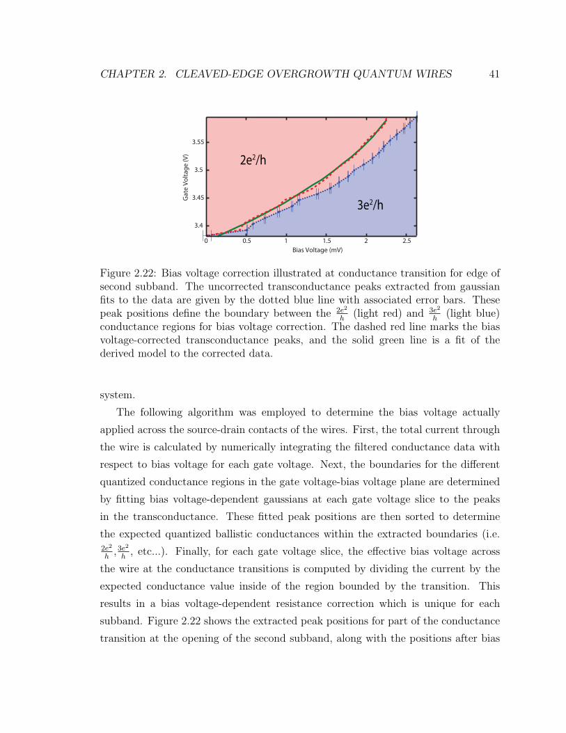
CHAPTER 2. CLEAVED-EDGE OVERGROWTH QUANTUM WIRES 41
0.5 1 1.5 2 2.5
Bias Voltage (mV)
3.4
3.45
3.5
3.55
Ga
te V
olt
ag
e (
V)
0
2e2/h
3e2/h
Figure 2.22: Bias voltage correction illustrated at conductance transition for edge ofsecond subband. The uncorrected transconductance peaks extracted from gaussianfits to the data are given by the dotted blue line with associated error bars. Thesepeak positions define the boundary between the 2e2
h(light red) and 3e2
h(light blue)
conductance regions for bias voltage correction. The dashed red line marks the biasvoltage-corrected transconductance peaks, and the solid green line is a fit of thederived model to the corrected data.
system.
The following algorithm was employed to determine the bias voltage actually
applied across the source-drain contacts of the wires. First, the total current through
the wire is calculated by numerically integrating the filtered conductance data with
respect to bias voltage for each gate voltage. Next, the boundaries for the different
quantized conductance regions in the gate voltage-bias voltage plane are determined
by fitting bias voltage-dependent gaussians at each gate voltage slice to the peaks
in the transconductance. These fitted peak positions are then sorted to determine
the expected quantized ballistic conductances within the extracted boundaries (i.e.2e2
h,3e
2
h, etc...). Finally, for each gate voltage slice, the effective bias voltage across
the wire at the conductance transitions is computed by dividing the current by the
expected conductance value inside of the region bounded by the transition. This
results in a bias voltage-dependent resistance correction which is unique for each
subband. Figure 2.22 shows the extracted peak positions for part of the conductance
transition at the opening of the second subband, along with the positions after bias

CHAPTER 2. CLEAVED-EDGE OVERGROWTH QUANTUM WIRES 42
voltage correction in the gate voltage-bias voltage plane.
The transconductance plots in the magnetic field-gate voltage plane were made
at zero DC source-drain bias, so no similar series resistance removal was necessary.
However, the positions of the transconductance peaks were extracted via the same
procedure described above.
2.5.3 Model Fitting
Figure 2.23 shows the transconductance for a CEO hole wire, where high values of
transconductance (dark features) indicate a transition. We model the CEO wire
band structure with a parabolic dispersion, which again yields the spin-degenerate
1D density of states of 2.10. Proceeding in a vein similar to the electron wire analysis,
we self-consistently solve 2.6 and 2.9 to find analytic expressions for the transition
curves, where the number of left- or right-movers is fixed. Unlike the electron wire
analysis, for the hole wires, the changing geometric capacitance across different sub-
band transitions was encoded by using a distinct but constant geometric capacitance
for the curves of each diamond. This was necessary due to the limited visibility of
the lower, upward sloping transitions in the hole wire data, which we discuss below.
In such a model, the geometric capacitance essentially jumps in discrete amounts at
the opening of a new subband. This was acceptable because only transitions of one
type are present in the data. However, when transitions of both types are present in
the data, using a model with jumps in the capacitance produces curves that do not
properly intersect at the zero bias vertices, and are therefore a poor match with the
transconductance data.
The derived curves for the visible conductance transitions were fit to the extracted
transconductance peaks using nonlinear least-squares regression by adjusting for each
curve the parameters ∆j+1,j and α = eℓ√2m⋆
Cπℏ . From the fits to the transition at the
second subband (marked by ), and using an effective mass m⋆ ≈ 0.5me, we extract
a geometric capacitance C =57.6aF and subband spacing ∆2,1 =2.5meV, which agree
well with estimates of these parameters based on the geometry of the hole wire.
The spatial distribution of charge carriers in CEO wires is set mostly by the

CHAPTER 2. CLEAVED-EDGE OVERGROWTH QUANTUM WIRES 43
-2 0 2 4-4
3.8
3.6
3.4
3.2
3
2.8
2.6
4in
cre
asin
g d
en
sitsy
Source-Drain Bias (mV)
Ga
te V
olta
ge
(V
)
Figure 2.23: CEO Hole wire transconductance and corresponding fits to the conduc-tance transitions overlaid in white. High transconductance is shown in black. Con-ductance transition fits are only given for the most visible transitions. The pinch-offvoltage is indicated by , and the edge of the second subband at zero bias by
growth, as in carbon nanotubes and vapor-liquid-solid-grown semiconductor nanowires.
This leads to a well-defined geometric capacitance, making our analysis approach ap-
plicable. Still, like the electron wires, one would expect some change in C for increas-
ing charge density as confinement is altered by the gate voltage and carriers spill out
of the CEO wire into the AlGaAs cladding. This is consistent with the the extracted
parameter values for transitions at higher subbands, where we find at the third sub-
band C =56.4aF and ∆3,2 =0.7meV, and at the fourth subband C =65.8aF and
∆4,3 =0.6meV. Additionally, a varying hole effective mass with subband occupation
may also influence the extracted values of these parameters.

CHAPTER 2. CLEAVED-EDGE OVERGROWTH QUANTUM WIRES 44
2.5.4 Hole wire transconductance discussion
As mentioned above, when comparing the hole wire transconductance with the elec-
tron wire transconductance, we see that the visibility of the upward-sloped transitions
is significantly reduced in comparison to the downward-sloped transitions. We distin-
guish between two types of transitions at non-zero source-drain bias, enclosed by the
ellipses in figure 2.24a,b. In a simplified picture, transport in a 1D subband can be
described in terms of left-movers and right-movers, which each contribute e2
hto the
conductance in a non-interacting wire. For the first type of transition (figure 2.24d),
the edge of a subband is aligned with the chemical potential of the left lead, so that
right-movers are injected into the subband as the bias voltage is modulated during a
conductance measurement. The chemical potential of the right lead is below the edge
of the subband, so no left-movers are present in the subband. For the second type
of transition (figure 2.24e), the chemical potential of the right lead is now aligned
with the edge of the subband, while the chemical potential of the left lead is above
the subband edge. This means the conductance transition occurs here as left-movers
are injected into a subband that is already populated by right-movers. These two
types of transitions should yield identical jumps in differential conductance of e2
hin
the ideal case of a non-interacting, ballistic 1D wire, shown schematically in figure
2.24a. In the presence of charge interactions, however, one might expect a reduction
in the conductance step for this type of transition, as the left-movers are scattered
by the right-movers.
Figure 2.24b shows the transconductance, the magnitude of the numerical deriva-
tive of the measured differential conductance with respect to gate voltage, for a hole
wire, where high values of transconductance indicate a transition. The expected
positions of the two transition types for the second subband are encircled by the
dashed ellipses. The transition associated with figure 2.24d is clearly visible. Unlike
these visible transitions which involve unidirectional dynamics, the visibility of the
transition associated with figure 2.24e is greatly reduced. This is true for the con-
ductance transitions of the first and third subbands as well. We postulate that the
reduction in visibility of these transitions may relate to charge interactions involving
scattering between right-movers and left-movers as described above. These results

CHAPTER 2. CLEAVED-EDGE OVERGROWTH QUANTUM WIRES 45
eV SD
d) e)
µL
3
c)
Ga
te V
olta
ge
(V
) Conductance Transitions
Source-Drain Bias (mV)
incre
asin
g d
en
sitsy
a)
Transconductance
-2 0 2
b)
4-4
10
0
Inte
nsity
(a.u
.)
(c)
(e)
(d)
0
µR
eV SD
Δ 2-1
Δ 3-2
2
1
(c)
(e)
(d)
3.8
3.6
3.4
3.2
3
2.8
2.6
4
Figure 2.24: a) Schematic diagram of ballistic hole wire conductance transitions. Thesolid lines indicate conductance transitions where the edge of a 1D hole subbandwithin the wire is energetically aligned with the chemical potential of either the left(source) or right (drain) leads. b) Transconductance of experimentally-measured holewire conductance. The white lines on the left half are fits to the data based on theballistic wire model described in the text. c) Hole dispersion for conditions markedby white triangle in (a) and (b). The inter-subband energy splittings are indicated onthe diagram. d) Hole dispersion for the conductance transition marked by the lowerdashed ellipse in (a) and (b). There are no left-movers in the second subband for thistransition. e) Hole dispersion for the conductance transition marked by the upperdashed ellipse in (a) and (b). The visibility of this transition in the measurement isstrikingly reduced compared to the transition in (d), which we postulate may be theresult of interactions between the left-movers and right-movers present in the subbandfor the transition.

CHAPTER 2. CLEAVED-EDGE OVERGROWTH QUANTUM WIRES 46
contrast with those in other 1D mesoscopic systems, where both types of transitions
are visible [70, 15, 20].
From our analysis, we find that the extracted geometric capacitance does not
monotonically increase as a function of increasing subband index. This may be un-
derstood by considering charge interactions beyond the Hartree term in (2.13). Such
interactions can be described by an additional capacitance term Cxc which adds in
series with the quantum capacitance (described in Chapter 2) and geometric capaci-
tance [36, 48]. As the quantum capacitance is already accounted for by the density of
states in our model, Cxc can be considered a correction to the geometric capacitance.
This correction is expected to be negative at low densities and become more positive
with increasing density, resulting in a capacitance decrease that competes with the
standard increase due to reduced confinement. With such an additional capacitance,
the effective geometric capacitance can be written as:
C ′geom =
Cgeom
1 + γ, (2.29)
where γ is the capacitance ratio Cgeom/Cxc. Theoretical calculations suggest γ can be
negative at low densities and crossover to positive values at higher densities, which
would give rise to a decreasing effective geometric capacitance with increasing sub-
band index. Future measurements on wires with reduced disorder should allow for
more careful examination of the influence of charge interactions and resulting modi-
fications to the geometric capacitance.
2.6 g-factor measurements
We further apply our analysis approach to conductance measurements in magnetic
field, where spin-polarized transport allows us to probe g-factor anisotropy associated
with strong spin-orbit coupling predicted in these wires [17, 78].

CHAPTER 2. CLEAVED-EDGE OVERGROWTH QUANTUM WIRES 47
Increasing B-field
E
Incr
ea
sin
g B
-fie
ld
Gate Voltage (V)
a) b)
Figure 2.25: Influence of magnetic field on 1D subbands. a) Spin-degenerate subbandsat zero magnetic field are split in energy and evolve into spin-polarized subbands asthe field increases. b) Spin-degenerate conductance plateaus at zero magnetic fieldevolve into spin-polarized plateaus as the magnetic field is increased. The positions ofthe conductance transitions can be tracked and plotted in the gate voltage-magneticfield plane. These transitions divide the plane into distinct regions of quantizedconductance, shown in the colored overlay.
2.6.1 Qualitative discussion of 1D magnetotransport
We begin by discussing qualitatively the effect of a magnetic field on 1D subbands, as
illustrated schematically in 2.25a,b. The spin-degenerate subbands at zero magnetic
field split into two spin-polarized subbands as the field increases. This is shown in (a),
where the bottoms of the subbands are separated in energy by gµBB, where g is the
g-factor and µB is the Bohr magneton.. In addition to this Zeeman splitting, there is
also a uniform shift in energy of both subbands due to orbital effects associated with
threading magnetic flux through the cross-section of the wire. For this discussion,
we ignore explicit effects of spin-orbit coupling beyond modifying the g-factor. Such
effects are explored further in a later section in this chapter.
Accompanying the spin-splitting of the subbands as the magnetic field is increased
is a splitting of the spin-degenerate conductance plateaus as the magnetic field is
increased. This is illustrated in 2.25b, where a spin-degenerate conductance plateau of
value 2e2
his split into two plateaus, one at e2
h, and one at 2e2
h. We can imagine tracking

CHAPTER 2. CLEAVED-EDGE OVERGROWTH QUANTUM WIRES 48
the positions of the conductance transitions between plateaus in the gate voltage-
magnetic field plane, and plotting the resulting transition curves in a manner similar
to the analysis of the nonlinear transport transconductance data. These transition
curves divide the plane into separate conductance regions, which we display with the
overlay in (b).
2.6.2 Zeeman splitting in CEO Hole Wires
In an external magnetic field B, the dispersion for a spin-polarized subband becomes
ϵ↑,↓i (k) → ϵi(k) ± 12gµBB + βB. The first additional term in the dispersion is the
magnetic Zeeman energy associated with a spin-up(+) or spin-down(-) subband. The
second additional term reflects the orbital energy associated with the magnetic vector
potential to first order in B, which has the same sign regardless of spin polarization.
Inclusion of this term is necessary to reproduce the observed transconductance curves,
and is physically justified, since at large B ∼9T, this term is on the order of the
subband splitting (for B ∼9T, ℏωc ∼ 3 meV, which is on the order of the subband
splitting ∆2−1). At first glance, it might appear that this orbital correction violates
time reversal symmetry, but this is not the case. Upon time reversal, in addition to
the magnetic field changing sign, the prefactor β also changes sign. This prefactor
is analogous to the magnetic quantum numbers that arise in the well-known Fock-
Darwin spectrum, where a magnetic field is applied along the axis of a cylinder[35,
21].7
Figure 2.26a shows the conductance of a hole wire as a function of gate voltage
and magnetic field, with external magnetic field oriented parallel to the wire axis.
The data are taken at the second conductance plateau, where the spin-polarized
subband splitting is clearly resolved, as indicated by the distinctly colored regions
in the plot.8 The transport in the central white region is spin-polarized. Such clear
spin-polarization has not been previously observed in electron wires. Our analysis
7It should be noted that in other studies such as [20, 19], this orbital term is not included in theanalysis despite the curvature of the features in the data.
8These data are not corrected for series resistance, so the conductance values are reduced fromthe ideal ballistic values.

CHAPTER 2. CLEAVED-EDGE OVERGROWTH QUANTUM WIRES 49
a) b)Parallel Field Perpendicular Field
Gate Voltage (V)3.1 3.2 3.3 3.4 3.53.1 3.2 3.3 3.4 3.5
8
0
2
4
6
Ma
gn
eti
c F
ield
(T
)
Co
nd
ucta
nce
(e /h
)2
0
4
2
3
1.5
0
Figure 2.26: Magnetoconductance of CEO hole wires. a) Conductance of hole wireat opening of second subband as a function of gate voltage and magnetic field ori-ented parallel to axis of wire. The black lines are fits to conductance transitionsassociated with spin-resolved subbands. b) Conductance of hole wire at second sub-band for magnetic field oriented perpendicular to axis of wire. Spin-resolved subbandtransitions are not visible here for fields below ∼5T, indicating a highly anisotropicg-factor associated with strong spin-orbit coupling. Spin-splitting develops at highfields, indicated by the plateau region enclosed by the dashed line.
focuses on the second subband, since the conductance at first subband is dominated
by disorder[78].
At zero source-drain bias, the curves for the conductance transitions in the gate-
voltage-magnetic field plane V ⋆↑,↓gate = f(B) are generated as follows. Consider the
spin-polarized subbands that arise from the second zero-field subband. The density
of spin-up/spin-down electrons in this subband is held constant at zero as a function
of gate voltage and magnetic field along these transition curves. Therefore, for the
curve associated with the spin-up subband, after integrating over the density of states:
N = N↑1 +N↓
1 = λ(eVgate−e2N
Cgeom
+1
2µBB−βB)
12 +λ(eVgate−
e2N
Cgeom
− 1
2µBB−βB)
12 ,
(2.30)
where λ =√
m∗
2ℏ2π2 . The condition for zero spin-up density in the second zero-field

CHAPTER 2. CLEAVED-EDGE OVERGROWTH QUANTUM WIRES 50
subband is simply:
eVgate −e2N
Cgeom
+1
2µBB − βB −∆2−1 = 0. (2.31)
Combining (2.30) and (2.31), we find for the transition curve:
eV ∗↑gate = (
e2λ
Cgeom
) ∗ [(∆2−1)12 + (∆2−1 − gµBB)
12 ] + ∆2−1 −
1
2gµBB + βB. (2.32)
The curve associated with the second spin-down subband is generated similarly by
making the appropriate modifications to (2.31) and (2.32) to reflect the non-zero
density of second subband spin-up electrons and constant zero density of second
subband spin-down electrons.
The positions of transconductance peaks in the gate voltage-magnetic field plane
were extracted similarly to the extraction of the transconductance features in the
nonlinear transport data. Both the spin-down subband and spin-up subband curves
were fit to the extracted peak positions simultaneously, using capacitance and sub-
band energy gap values obtained from the nonlinear transport measurements. From
the fitting, we find a g-factor of g ≈ 2.1 for this parallel field orientation. The fits to
the conductance transitions are superimposed on the 2D conductance map as black
lines, marking the boundaries between spin-polarized conductance plateaus. How-
ever, for figure 2.26b where the external magnetic field is oriented perpendicular to
the axis of the wire, no clear subband splitting is observed below B ∼5T. Based on
the precision of this data, we estimate a lower bound on the ratio of the parallel to
perpendicular g-factors to be g∥/g⊥ ∼ 50 in this field regime, demonstrating the high
degree of anisotropy in the g-factor for CEO hole wires. Spin-splitting does develop
at high fields for this orientation, indicated by the white plateau region bounded by
the dashed line in figure 2.26b.
As confirmation for the validity of our analysis, we present in figure 2.27 nonlinear
transconductance data as a function of gate voltage and source-drain bias with B =
9T for the parallel field orientation. Tracking the conductance transitions for the
spin-polarized subbands shown in the inset allows for a direct measurement of gµBB,

CHAPTER 2. CLEAVED-EDGE OVERGROWTH QUANTUM WIRES 51
Ga
te V
olta
ge
(V
)
Source-Drain Bias (mV)
gµB
0-2 2-1 13.5
3.3
3.1
2.9B = 9T
gµBeV SD
Figure 2.27: Hole wire nonlinear transconductance in static 9T field oriented parallelto axis of wire. The dotted lines are guides indicating conductance transitions associ-ated with the spin-resolved subands of 2.26a. The intersection of these features (whitediamond) allows for a direct, independent estimate of the g-factor, which agrees wellwith the value extracted from the model. Inset: subband energetic configuration atthe transition intersection point marked by the white diamond.
independent of the transport model [71]. From this analysis, we extract a value of
g ≈ 2, which matches well with the g-factor obtained from our ballistic transport
model analysis.
2.7 0.7 Structure in CEO Hole Wires
The upper pane of figure 2.28 shows individual conductance traces near the edge
of the second subband as for fields between 0 and 9T. The conductance for the
individual traces has been normalized for clarity to a fixed value at high density to
offset the orbital dependence of the conductance on magnetic field. As the magnetic
field is decreased from 9T, the spin-polarized conductance half-step merges into the

CHAPTER 2. CLEAVED-EDGE OVERGROWTH QUANTUM WIRES 52
1
1.5
2
2.5
3.1 3.2 3.3 3.4 3.5
1
1.5
2
2.5
3
Co
nd
ucta
nce
(e
/h
)2
Gate Voltage (V)
8
0
2
4
6
Ma
gn
eti
c F
ield
(T
)
4
5
10
15
20
25
0T
9T
Figure 2.28: 0.7 structure at the second hole wire subband. The upper pane showsnormalized zero-bias conductance traces at the opening of the second subband from0 to 9T. As the magnetic field is decreased from 9T the spin-resolved conductancehalf-step merges into the 0.7-like feature at low field. This evolution is also shown inthe transconductance plot in the lower pane, where the dark transition features donot merge at zero field.
zero-field conductance anomaly indicated by the arrow, which we associate with 0.7
structure. Such a feature has been observed in numerous other 1D nanostructures[26,
19, 15], and is thought to be related to electron-electron interactions, since it cannot
be explained by simple free electron transport models. The transconductance of this
data is plotted in the lower pane, where 0.7 structure prevents the spin-polarized
conductance transitions from merging at zero field.

CHAPTER 2. CLEAVED-EDGE OVERGROWTH QUANTUM WIRES 53
2.7.1 Hole wire degeneracy
To confirm that these features can be associated with 0.7 structure, we must make
an estimate of the hole wire degeneracy for this subband. Ignoring spin degeneracy,
the density of carriers in a subband of a 1D wire can be written simply as:
ni =
(√2m∗
πℏ
)·√EF − Ui, (2.33)
where the “i” subscript refers to the subband index, and Ui is the energy of the
bottom of the subband.
We can also estimate the total carrier density in the wire using the simple ca-
pacitance relation ntotal =C∆Vg
eL, where C is the geometric capacitance, L is the wire
length, and ∆Vg is the gate voltage measured from pinch-off. We would like to find
the difference in energy between the Fermi energy and the bottom of the second
(spin-polarized) subband: ∆E = EF −∆2, where ∆2 is the energy spacing between
the bottoms of the first and second subbands. This Fermi energy corresponds to the
gate voltage Vg shown in figure 2.29 At this gate voltage, there is a spin-degenerate
subband occupied (first subband) and another occupied subband (second subband),
which is either spin-polarized or spin-degenerate, depending on interpretation. We
will assume this subband is also spin-degenerate, and using the above equations, we
can relate the Fermi energy to the gate voltage span:
C∆Vg
eL=
(2√2m∗
πℏ
)· (√EF +
√EF −∆2). (2.34)
This equation can be easily solved numerically. The values for the various wire
parameters are given in the table 2.2, where C and ∆2 have been extracted from the
nonlinear transport measurements:
Using these values, we find ∆E ∼ 38µV, which corresponds to a Fermi tem-
perature (with respect to the bottom of the second subband) of TFermi = 400mK.
Since the temperature for these measurements was T = 450mK, the hole gas is non-
degenerate, i.e. Tbath ∼ TFermi. This means the wire is in the temperature regime

CHAPTER 2. CLEAVED-EDGE OVERGROWTH QUANTUM WIRES 54
pinch-oVgV
gΔV =0.7V
2nd plateau
Figure 2.29: Conductance features used in hole wire degeneracy calculation. Themagnetic field is applied along the wire axis. The gate voltage Vg marks the relevantconductance step. Measured from the pinch-off voltage, this corresponds to ∆Vg =0.7V.
Table 2.2: Values of CEO hole wire parameters used in degeneracy calculationParameter ValueL 2µmC 57.6aF∆2 2.5meV∆Vg 0.7Vm∗ 0.5me
where one expects to observe 0.7 structure, and it is consistent with previous studies
to associate the additional conductance plateau associated with the second subband
at low magnetic fields with this structure[26].
2.8 Spin-Orbit Coupling in 1D
We now begin our discussion of spin-orbit coupling in 1D[78]. Such spin effects have
important technological relevance; for example, understanding the flow of spins in
magnetic layered structures has resulted in an increase in data storage density in
hard drives over the past decade of more than two orders of magnitude. The field

CHAPTER 2. CLEAVED-EDGE OVERGROWTH QUANTUM WIRES 55
of “spintronics” aims to move beyond technologies based on local spin polarization,
and use spin-orbit interaction effects to manipulate spin currents for information
transmission[34, 11, 91]. As we show below, spin-orbit coupling has a dramatic effect
on the conductance of a 1D device, in contrast to two- and three-dimensional samples,
where the effect is more elusive and requires sophisticated detection schemes[53, 80,
56, 38, 12, 100]. Here we present the first observation of a predicted spinorbit gap in
1D, where counter-propagating spins, constituting a spin current, are accompanied
by a clear signal in the linear conductance of the system[73, 105].
2.8.1 Overview of Spin-Orbit Coupling
Spin-orbit coupling arises as a relativistic correction to the Hamiltonian of a charged
particle moving through an electric field. In the rest frame of the charged particle, a
magnetic field arises through Lorentz transformation of the electric field. This mag-
netic field will interact with the magnetic moment of the charged particle, requiring a
perturbation of the non-relativistic Hamiltonian[45]. For an electron moving through
an atomic potential V , this correction is:
HSO = − ℏ4m2
0c2σ · p× (∇V ), (2.35)
where m0 is the free electron mass, σ are the pauli spin matrices, and p is the mo-
mentum operator. This is known as the Pauli spin-orbit interaction. When combined
with k · p-theory and the envelope function approximation in a semiconductor, the
Pauli spin-orbit interaction leads to the following modification of the Hamiltonian:
HSO = βσ · k ×∇V ≡ βσ ·BSO, (2.36)
where k is the electron momentum, and β is a material-dependent constant[97, 32].
The effective magnetic field BSO is therefore directly related to the electric field
ESO ≡ |∇V |, as described qualitatively above. This electric field can arise from two
different asymmetries in the solid state. Bulk inversion asymmetry occurs when the
underlying lattice lacks an inversion center, giving rise to the so-called “Dresselhaus”

CHAPTER 2. CLEAVED-EDGE OVERGROWTH QUANTUM WIRES 56
Figure 2.30: Spin-orbit coupling in a 1D subband. A spin degenerate subband (a)evolves into two spinful subbands shifted in wavevector under the influence of spin-orbit coupling (b).
spin-orbit coupling. Alternatively, structural inversion asymmetry arises from exter-
nal confining electric fields, such as those that from materials interfaces and gate
electrodes in heterostructures, causing the so-called “Rashba” spin-orbit coupling.
Both asymmetries are relevant for the CEO hole wires, though the Rashba spin-orbit
coupling appears most important for determining the direction of the effective spin-
orbit magnetic field BSO. We discuss these effects quantitatively in the context of the
GaAs hole band structure in the later section on modeling the observed 1D spin-orbit
gap.
Consider a spin-degenerate one-dimensional (1D) sub-band without spin-orbit cou-
pling, as shown in figure 2.30a. Upon inclusion of the spin-orbit correction to the
Hamiltonian (2.36), the spin-degeneracy is lifted and the spinful subbands shift lat-
erally in wavevector, shown in figure 2.30b. Mathematically, this is simply explained
by “completing the square” in the Hamiltonian:
H =ℏ2k2
2m± βkESO =
ℏ2(k ± kSO)
2m+ constant, (2.37)
where kSO = βmESO/ℏ2. However, despite the striking shift in bandstructure, the
conductance through the subbands is equal to the conductance in the case of no spin-
orbit coupling. This is because the edges of the spinful subbands are still degenerate,
resulting in a conductance of G = 2e2
h.

CHAPTER 2. CLEAVED-EDGE OVERGROWTH QUANTUM WIRES 57
k
E
k
E
Spin-polarized current!
Gate Voltage
1
0
G (
2e
2/h
)
Gate Voltage G
(2
e2/h
)
1
0
a) b)
ΔSO
Figure 2.31: Spin-orbit coupling in a 1D subband with external magnetic field. a)External magnetic field applied parallel to spin-orbit field (Bext ∥ BSO) lifts thedegeneracy between the spin-polarized subbands, but leading to a conductance in-distinguishable from the case with no spin-orbit coupling. b) External magneticfield applied perpendicular to spin-orbit field (Bext ⊥ BSO) results in an anticrossingbetween spinful subbands, creating a gap ∆SO and yielding a qualitatively distinctconductance and spin-polarized current at zero bias voltage.
We now investigate the influence of an external magnetic field on this 1D subband
with spin-orbit coupling. First, consider the case where the external field is applied
parallel to the intrinsic spin-orbit field (Bext ∥ BSO). Working in the | k⟩⊗
|↑, ↓⟩basis, with the spin-orbit field along the z−axis, the Hamiltonian for each k−state in
the subband becomes:
H∥ =ℏ2
2m
(k2 0
0 k2
)+ βkESO
(k 0
0 −k
)+
1
2gµBBext
(1 0
0 −1
). (2.38)
This Hamiltonian is already diagonalized, and the dispersion is plotted in figure 2.31a.
The external magnetic field splits the spin-up and spin-down subband edges in energy
by the Zeeman energy, but does not otherwise modify the parabolic dispersions. This
leads to a conductance that is once again indistinguishable from the case when no
spin-orbit coupling is present, as the measured conductance will be equivalent to the

CHAPTER 2. CLEAVED-EDGE OVERGROWTH QUANTUM WIRES 58
conductance through the spin-polarized subbands discussed in section 2.6.
Now, consider the external magnetic field aligned perpendicular to the intrinsic
spin-orbit field (Bext ⊥ BSO). For this field orientation, the Hamiltonian becomes:
H∥ =ℏ2
2m
(k2 0
0 k2
)+ βkESO
(k 0
0 −k
)+
1
2gµBBext
(0 1
1 0
). (2.39)
This Hamiltonian is no longer in diagonal form, and the resulting dispersion contains
an anticrossing between the two spinful subbands at k = 0, with a splitting we term
the “spin-orbit gap”. shown in 2.31b. The corresponding conductance is qualitatively
different from the case where the external field is parallel to the spin-orbit field. For
this perpendicular case, the conductance is 2e2
hwhen the Fermi level outside of the
gapped region, but drops to e2
hin the gap, as the number of left-mover/right-mover
branches is reduced by two. Additionally, the transport in the gapped region is
completely spin-polarized in a way that is expected to be robust against moderate
disorder: for backscattering to occur, carriers must scatter from the +k-states to the
−k-states as well as undergo a spin flip. The direction of spin current in this system
of counter-propagating spins (very nearly what is termed a ‘helical liquid’[98]) is
independent of the sign of the bias voltage applied across the channel, and is instead
determined by the spin-orbit coupling. In fact, at zero bias voltage, a pure spin
current exists without any accompanying charge current. Figure 2.32 summarizes
these magnetic field/spin-orbit effects for a model that includes two subbands[73].
2.8.2 Experimental observation of spin-orbit gap
We now present our transport measurements of CEO hole wires in magnetic field
as in section 2.6.2, but now over an extended gate voltage range to include higher
subbands.
Figure 2.33a,b shows the main experimental results, taken at T = 300mK. We
orient the axes such that the wire axis is in the x-direction, and first discuss 2.33a,
where Bext is applied perpendicular to the wire axis, but in the plane of the 2DHG
(to prevent Landau level formation) along the y-direction. We see that the second,

CHAPTER 2. CLEAVED-EDGE OVERGROWTH QUANTUM WIRES 59
E
k
E
E
k
k
B=0
BSO
BSO
BSO
B
B
0 1 2
0 1 2
0 1 2
Ga
te V
olta
ge
Ga
te V
olta
ge
Ga
te V
olta
ge
Conductance (2e /h)2
Conductance (2e /h)2
Conductance (2e /h)2
a)
b)
c)
Figure 2.32: Dispersions and associated conductance for multiple 1D subbands withspin-orbit coupling with various configurations of external magnetic field. a) Noexternal magnetic field. b) External field applied parallel to spin-orbit field. c)External field applied perpendicular to spin-orbit field.
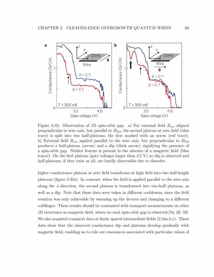
CHAPTER 2. CLEAVED-EDGE OVERGROWTH QUANTUM WIRES 60
Figure 2.33: Observation of 1D spin-orbit gap. a) For external field Bext alignedperpendicular to wire axis, but parallel to BSO, the second plateau at zero field (bluetrace) is split into two half-plateaus, the first marked with an arrow (red trace).b) External field Bext applied parallel to the wire axis, but perpendicular to BSO
produces a half-plateau (arrow) and a dip (thick arrow), signifying the presence ofa spin-orbit gap. Neither feature is present in the absence of a magnetic field (bluetraces). On the first plateau (gate voltages larger than 3.5 V) no dip is observed andhalf-plateaus, if they exist at all, are hardly discernible due to disorder.
higher conductance plateau at zero field transforms at high field into two half-height
plateaus (figure 2.33a). In contrast, when the field is applied parallel to the wire axis
along the x-direction, the second plateau is transformed into two-half plateaus, as
well as a dip. Note that these data were taken in different cooldowns, since the field
rotation was only achievable by warming up the devices and changing to a different
coldfinger. These results should be contrasted with transport measurements on other
1D structures in magnetic field, where no such spin-orbit gap is observed.[54, 20, 59].
We also acquired transport data at finely spaced intermediate fields (2.34a,b,c). These
data show that the observed conductance dip and plateaus develop gradually with
magnetic field, enabling us to rule out resonances associated with particular values of

CHAPTER 2. CLEAVED-EDGE OVERGROWTH QUANTUM WIRES 61
c)d)
Figure 2.34: CEO hole wire data continuity and reproducibility. a),b) Data fromFigure 2.33, with additional traces taken at intermediate fields (every 0.2T) showingthat the features (arrows) develop gradually with field and are not spurious effects.c) Data from (b) around the spin-orbit gap. d) Data from a separate device, showingthe dip on the second plateau resulting from the presence of the spinorbit gap.
the magnetic field as the cause of the observed features. In addition, these features-
and in particular the conductance dip-were observed in a separate device (2.34d) and
persist after thermal cycling; thus, they are also not linked to particular configurations
of the disorder potential in the device.
Let us try to understand these results in terms of the simple model presented in the
previous section. Assuming that the main contribution to the spin-orbit effect results
from structural inversion asymmetry (Rashba), we expectBSO to be perpendicular to
the wire, in the y-z plane, as the structure is translationally invariant along the length
of the wire. Thus, a magnetic field in the x-direction perpendicular to BSO should
produce dips in the zero-field conductance plateaus (as in figure 2.37c), whereas one in
the y-direction should split each zero-field conductance step into two half-plateaus (as

CHAPTER 2. CLEAVED-EDGE OVERGROWTH QUANTUM WIRES 62
Figure 2.35: 2D GaAs dispersions from [97]. The four-band Luttinger model describesthe HH and LH valence bands.
in figure 2.37b) and possibly also produce dips simultaneously. Our data bear more
than a passing resemblance to the expectations from the simple model, yet the two
are significantly different in their details. A more realistic model, described below,
enables us to more fully understand our results.
2.8.3 Modeling of spin-orbit gap dispersions
We begin with a four-band Luttinger model for the bulk GaAs[97]2.35 (not to be
confused with the Tomonaga-Luttinger liquid theory) This model, containing the
heavy-hole (HH) and light-hole (LH) valence bands, is valid for large-gap III-V semi-
conductors with band edges at the Γ-point. The Hamiltonian in the bulk is:
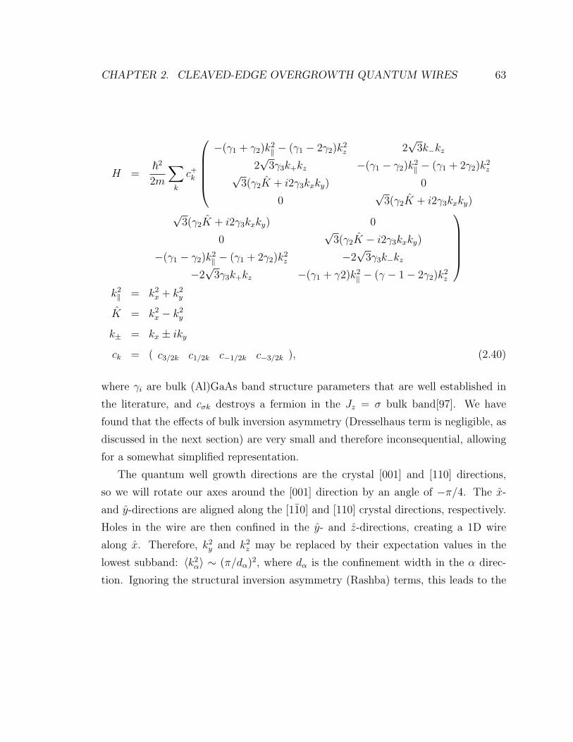
CHAPTER 2. CLEAVED-EDGE OVERGROWTH QUANTUM WIRES 63
H =ℏ2
2m
∑k
c+k
−(γ1 + γ2)k
2∥ − (γ1 − 2γ2)k
2z 2
√3k−kz
2√3γ3k+kz −(γ1 − γ2)k
2∥ − (γ1 + 2γ2)k
2z√
3(γ2K + i2γ3kxky) 0
0√3(γ2K + i2γ3kxky)
√3(γ2K + i2γ3kxky) 0
0√3(γ2K − i2γ3kxky)
−(γ1 − γ2)k2∥ − (γ1 + 2γ2)k
2z −2
√3γ3k−kz
−2√3γ3k+kz −(γ1 + γ2)k2
∥ − (γ − 1− 2γ2)k2z
k2∥ = k2
x + k2y
K = k2x − k2
y
k± = kx ± iky
ck = ( c3/2k c1/2k c−1/2k c−3/2k ), (2.40)
where γi are bulk (Al)GaAs band structure parameters that are well established in
the literature, and cσk destroys a fermion in the Jz = σ bulk band[97]. We have
found that the effects of bulk inversion asymmetry (Dresselhaus term is negligible, as
discussed in the next section) are very small and therefore inconsequential, allowing
for a somewhat simplified representation.
The quantum well growth directions are the crystal [001] and [110] directions,
so we will rotate our axes around the [001] direction by an angle of −π/4. The x-
and y-directions are aligned along the [110] and [110] crystal directions, respectively.
Holes in the wire are then confined in the y- and z-directions, creating a 1D wire
along x. Therefore, k2y and k2
z may be replaced by their expectation values in the
lowest subband: ⟨k2α⟩ ∼ (π/dα)
2, where dα is the confinement width in the α direc-
tion. Ignoring the structural inversion asymmetry (Rashba) terms, this leads to the

CHAPTER 2. CLEAVED-EDGE OVERGROWTH QUANTUM WIRES 64
following effective 1D Hamiltonian:
H1d =ℏ2
2m
∑k
c+k
−(γ1 + γ2)k
2x 0
0 −(γ1 − γ2)k2x −∆
i(√3γ2k
2x − βy) 0
0 i(√3γ2k
2x − βy)
−i(√3γ2k
2x − βy) 0
0 −i(√3γ2k
2x − βy)
−(γ1 − γ2)k2x −∆ 0
0 −(γ1 + γ2)k2x
ck
with
∆ = 4γ2π2
(1
d2z− 1
2d2y
),
βy =√3γ2
π2
d2y,
and the basis
ck = ( c0+3/2k c0+1/2k c0−1/2k c0−3/2k ), (2.41)
where the di represent the confinement in the i-direction. Here c0σk destroys a
fermion in the lowest confinement subband of the Jz = σ bulk band at momentum
k. We have chosen a pair of subbands arising from heavy-hole like states c0±3/2k,
and a pair of subbands arising from light-hole like states c0±1/2k. Although it is not
clear a priori which bulk bands give rise to the four lowest subbands, this choice is
motivated by the fact that, given Equation (2.41), the spacing between the chosen
subbands could be comparable to the inter-subband spacing of the heavy-hole-like
series of subbands. Thus, the two reasonable options seem to be either that the two
lowest sub-bands should be heavy-hole-like, or that one of them should be light-hole-
like. Our choice of the latter is subsequently validated by our data. The parameter
βy arises from the confinement in the y-direction.
We now return to the SIA (Rashba) terms. These may be deduced from symmetry,

CHAPTER 2. CLEAVED-EDGE OVERGROWTH QUANTUM WIRES 65
or more formally the method of invariants. For spin-3/2 systems, there are two allowed
Rashba terms which are linear in momentum: HSIA = α1(k× E) · J +α2(k× E) · J ′,
where J = (Jx, Jy, Jz) are spin 3/2 matrices and J ′ = (J3x , J
3y , J
3z ). Empirically
α2 ≪ α1, so we shall ignore the second term in (2.40). For the confinement electric
fields, we have Ez = 0 and Ez = 0 and thus the 1D Rashba term is
HR1d = α1kx(EyJz − EzJy)
=
32rykx
√64ϕ+rzkx 0 0
√64ϕ−rzkx
12rykx
√22ϕ+rzkx 0
0√22ϕ−rzkx −1
2rykx
√64ϕ+rzkx
0 0√64ϕ+rzkx −3
2rykx
(2.42)
where ry = α1Ey, rz = α1Ez, and ϕ± = 1 ± i are the strength of the Rashba
spin-orbit coupling.
Finally, we consider terms added to the Hamiltonian to describe the effects of an
applied external magnetic field, where we ignore orbital terms for simplicity. Two
Zeeman terms are expected for the spin-3/2 systems: HZ = g1µBB · J + g2µBB · J ′.
Here again g2 ≪ g1, so the second term can be ignored. In matrix form, the remaining
(first) term is:
HZ = gµB
32Bz
√64ϕ−B− 0 0
√64ϕ+B+
12Bz
√22ϕ−B+ 0
0√22ϕ+B+ − 1
2Bz
√64ϕ−B−
0 0√64ϕ+B+ −3
2Bz
, (2.43)
where B± = Bx ± iBy and ϕ± = 1± i. Our full model Hamiltonian is then:
H = H1d +HR1d +HZ . (2.44)
To calculate the dispersions, which we discuss in 2.8.4 below, we use the set of pa-
rameters listed in table 2.3.

CHAPTER 2. CLEAVED-EDGE OVERGROWTH QUANTUM WIRES 66
Table 2.3: Parameters and values used in 1D spin-orbit modelParameter Valueγ1 6.85 (5.68)γ2 2.1 (1.63)γ3 2.9 (2.35)χ 0.05dy 60nmdz 25nmry 0rz 23±2meV-nm
The numbers in brackets are for Al0.324Ga0.676As, calculated using a linear interpo-
lation in the virtual crystal approximation, while those not in brackets are for GaAs.
The actual numbers used in the model are γn = χγn,AlGaAs + (1 − χ)γn,GaAs, where
χ represents the leakage of the confined subband wavefunction into the AlGaAs (ef-
fectively modeling deviation from an infinite potential well). We estimated χ from
simulations of the wavefunction of the lowest bound state in the potential wells in
both confinement directions using the program developed by Gregory Snider for this
purpose, exploring a rather large range of possible effective masses (0.2-0.65 times the
bare electron mass), guided by theoretical values and the little that is experimentally
known about the effective masses in these systems. We obtained 0 < χ < 0.09 and
chose a value in the middle for the model. We note that χ is in any case a parameter
to which our results are rather insensitive.
The remaining four parameters dy, dz, ry, rz, are used as fitting parameters. They
are grouped into two two-parameter sets which are treated differently; dy and dz, the
confinement related parameters are constrained to reasonable values not too different
from an estimated extent of the wave function along these two directions. While the
thicknesses of the layers giving rise to the confinement are known to great accuracy,
since they are set by the MBE growth, the actual extent of the wavefunctions and the
precise relation of those to dy and dz are difficult to calculate. We have estimated the
extent of the wavefunction in each direction rather crudely by modeling two fictitious
two dimensional hole gases separately, neglecting the joint effect of both confinements
in the real device. The two 2DHGs were simulated using nominal growth parameters

CHAPTER 2. CLEAVED-EDGE OVERGROWTH QUANTUM WIRES 67
in each direction separately. We found the extent of the wavefunction in z to be about
15nm, while in y, we obtain about 30-35nm. The values for dy and dz used in the
model are within a factor of two of these figures.
The other two parameters, ry and rz, are simply tuned to match the model calcu-
lations to the data. The values found are in fact the first available estimates of these
parameters.
2.8.4 Modeled 1D spin-orbit dispersions and conductance
simulations
Figure 2.36 shows the calculated dispersions from the above Hamiltonian and the
corresponding simulated conductance traces. The dispersions were generated by nu-
merically diagonalizing the Hamiltonian, and the conductance traces were numerically
evaluated in the following manner from the dispersion relations. First, the conduc-
tance as a function of the chemical potential was obtained within a non-interacting
electron model using the Landauer-Buttiker formalism and the calculated dispersions.
Next, the dependence of the hole density on the chemical potential was calculated,
then translated into the gate voltage as a function of the chemical potential using
the wire model described in 2.4.1 Finally, the gate voltage is related directly to the
conductance. Two additional parameters are used in this simulation: the gate volt-
age at pinch-off, where the density is zero, and the geometrical capacitance, 4.25V
and 20pF/m, respectively. The code for generating the dispersions and conductance
traces is described in appendix D.
Figure 2.36a shows the four lowest energy subbands calculated in the absence of
magnetic field. Focusing first on the upper pair of subbands, we see that applying a
field in the y-direction shifts them in energy (figure 2.36b), producing a double step
in the conductance trace (figure 2.36d), which is seen in our data (figure 2.33a). In
contrast, a field in the x-direction produces a gap in the band structure (figure 2.36c)
and a dip in the conductance trace (figure 2.36e), also seen in our data (figure 2.33b).
The spin splitting at B = 0 is much smaller for the lower pair of subbands than in
the upper subbands. Furthermore, as in our data, magnetic fields in both orientations

CHAPTER 2. CLEAVED-EDGE OVERGROWTH QUANTUM WIRES 68
Figure 2.36: Calculated 1D Dispersions from Luttinger model and associated simu-lated conductance traces. at the experiment temperature of 300mK. a) The dispersionrelations of the two lowest quantum wire sub-bands with no applied magnetic field.b) The same bands in a magnetic field of 9T perpendicular to the wire axis, withg = 2. c) The same bands in a magnetic field of 9T parallel to the wire, with g = 2/9.d) Conductance traces calculated from (a) (blue) and (b) (red). Compare to figure2.37a. e) Conductance traces calculated from (a) (blue) and (c) (red). Compare tofigure 2.37b.

CHAPTER 2. CLEAVED-EDGE OVERGROWTH QUANTUM WIRES 69
do not have much of an effect on the conductance through these lower subbands
(Figs 2.33. The small half-step in the red trace in figure 2.36d is likely obscured in
the data by disorder-related features near depletion. This suppression of the spin-
orbit coupling effects for this lower pair of subbands is a consequence of the fact that
these bands have been chosen in the model to be primarily of heavy-hole character-
their carriers have spin ±3/2- a choice motivated by our data and other physical
considerations as explicated in the previous section. The leading-order Rashba and
Zeeman terms are linear in spin operators and thus can couple only states with ∆S =
1. As ∆S = 3 for the heavy holes, the two lower subbands are not coupled by
these terms. Their coupling requires cubic-order terms in the spin operators. Such
terms, however, are small in all components of the Hamiltonian: Rashba and Zeeman
couplings that are cubic in spin operators do exist, but their coupling constants are
suppressed[97]. The lowest order Dresselhaus term is cubic in spin operators, but
in GaAs it is again very small and thus has almost no effect on the subbands[97].
Indeed, the Dresselhaus term has a minimal effect not only on the lower subbands,
but on the upper pair of subbands as well. Therefore, the spin-orbit effects seen in
our samples come primarily from the asymmetry of the confining potential of the 1D
wire, that is, the Rashba term. We find further that the electric field associated with
this potential is stronger in the z- than in the y-direction.
Regarding the g-factor, we find that to simulate the experimentally observed
conductance features at an external magnetic field of 9T field, our model requires
an effective g-factor ∼2 in the y-direction and an effective g-factor ∼2/9 in the x-
direction (figures 2.36d,e). This anisotropy is expected for such strong spin-orbit
coupling[97, 54, 20], though we note that these g-factor values at Bext =9T are dif-
ferent from the experimentally determined g-factors in section 2.6.2. However, one
must be wary when discussing effective g-factors in the presence of spin-orbit cou-
pling, as quantities commonly interpreted as ‘spin splittings’ are not necessarily equal
to g⋆µBB, where g⋆ is the effective g-factor in the Zeeman term in the Hamiltonian.
For example, in the simple 1D model described in figure 2.32, the situation in figure
2.32c could be interpreted as g⋆ = 0 on the basis of measurements of sub-band edges,
whereas g⋆ = 0 in the model is most definitely finite.)

CHAPTER 2. CLEAVED-EDGE OVERGROWTH QUANTUM WIRES 70
We note that the nonlinear transport measurements in the same device point to
a subband spacing of about 3meV, which is slightly smaller than what the model
predicts with the chosen parameters (∼4meV shown in figure 2.36a). This mismatch
is possibly due to the mixing with nearby subbands (next few conductance steps),
which is not considered in this model.
We are thus able to describe most of the important features of our data with the
proposed model and to identify their physical causes. Further theoretical work is
needed to understand one feature of our data that our model fails to capture: the
occurrence of a double plateau in addition to a dip when the magnetic field is applied
in the x-direction.
2.9 Future Directions
In closing, we have presented measurements of ballistic transport in CEO hole wires
and have developed a new approach to analyzing these measurements, which should
be widely applicable to other ballistic mesoscopic systems. From our analysis, we have
observed large g-factor anisotropy likely associated with predicted strong spin-orbit
coupling, and have found evidence for the importance of charge interactions in the
observation of 0.7 structure. We have also observed for the first time the spin-orbit
gap predicted for 1D systems, and we have developed a model that describes most of
the detailed features of our data by taking into account the materials properties of
(Al)GaAs [78].
Several directions seem promising for the further exploration of these wires. For
this particular device geometry, wires with less disorder would allow the study of
spin-orbit effects at finite bias voltage and in higher sub-bands. A tunneling geometry
could probe the dispersion relations directly[6], and a side gate would allow tuning
the strength of the electric field that gives rise to the spin-orbit effect[101]. For the
purposes of spintronics applications, verification of spin transport, particularly at
zero bias, would be of great interest. This could be achieved either through direct
detection of the spin current or through the detection of spin accumulation at the
two ends of the device. It would also be of practical interest to explore the possibility

CHAPTER 2. CLEAVED-EDGE OVERGROWTH QUANTUM WIRES 71
of producing such spin-orbit gaps in the lowest sub-band and without a magnetic
field, perhaps through the use of materials with magnetic order or through controlled
doping with magnetic impurities. Finally, it would be interesting to introduce tunnel
barriers into the wire through side gates or through the MBE growth. These barriers
could be used to perform the Luttinger liquid tunneling experiments described in
Chapter 4, or to produce quantum dots coupled to 1D leads.

Chapter 3
Quantum Capacitance
3.1 Introduction
As discussed in chapters 2 and 4, imperfect contacts and disorder-induced scatter-
ing in nanostructures strongly influence conventional transport (i.e. conductance)
measurements and greatly complicate their interpretation. In 1D systems, where the
surface-to-volume ratio is maximally skewed, such effects can completely dominate
the conductance features associated with the bandstructure of the system under test,
which are most often the results desired from the measurement. Unless the fea-
tures of a conductance measurement can be directly correlated to some energy scale
(e.g. Coulomb blockade peak spacing as a function of gate voltage), the absolute
conductance values obtained in such measurements provide limited insight into the
underlying physics. One can hope to extract meaningful, quantitative results from
such measurements through the use of transport models that incorporate disorder,
contact resistance, and other relevant scattering mechanisms (e.g. phonons), though
this is often quite difficult in practice and results are highly dependent upon the
simplifying approximations that are often made in these models.
However, as we show below, one can directly obtain a clear, detailed picture of
electronic bandstructure through high-resolution measurements of the capacitance.
In these measurements, the so-called “quantum capacitance” is extracted, which is
directly proportional to the system’s density of states. When applied to 1D systems,
72
CHAPTER 3. QUANTUM CAPACITANCE 73
these quantum capacitance measurements allow for quantitative study of charge in-
teractions and other such effects that modify the bandstructure. These quantum
capacitance measurements can additionally be performed on nanoscale systems of
practical interest to extract physical parameters that are crucial for assessing de-
vice performance. For example, mobility, an important parameter in nanoscale de-
vice engineering, cannot be accurately characterized from conductance alone without
knowing the exact carrier density from capacitance measurements, as we will show
below.
In this chapter, we develop the concept of quantum capacitance[23, 67, 62] in
the context of a nanostructure that is capacitively-coupled to a gate electrode. We
propose a series of quantum capacitance measurements for carbon nanotubes and
graphene nanoribbons, and discuss how conventional capacitance measurement tech-
niques are inadequate to perform these measurements. We next present the design
and fabrication of a custom, ultra-high-resolution (aF) capacitance bridge, termed
the “integrated capacitance bridge,” capable of performing these proposed measure-
ments. Finally, as a demonstration of the integrated bridge’s performance, we present
quantum capacitance measurements of top-gated graphene devices (including a di-
version into gating and potential barriers in 2D graphene), as well as initial results
from capacitance measurements of carbon nanotubes.
3.2 Fundamentals of Quantum Capacitance
Figure 3.1 shows the familiar channel that is capacitively-coupled to a gate electrode,
and is ohmically-connected to an adjacent charge reservoir. The channel is no longer
restricted to just 1D, and the system is held at some non-zero temperature T . For
this general treatment, we have labeled the various energies in the diagram in a more
conventional manner, with the chemical potential µ referenced from grounded charge
reservoir. Using this notation, we rewrite equation (2.6):
eVg = µ+ eΦ, and Φ =eN
Cg
, (3.1)

CHAPTER 3. QUANTUM CAPACITANCE 74
k
ε(k)
E =Channel
Gate
C
Vg
g
e NC
2
eVg
μ
E =0
μ
g
a) b)
Figure 3.1: Subband schematic for quantum capacitance. a)Energy diagram of achannel capacitively-coupled to a gate electrode depicting (3.1). b) Schematic ofchannel with capacitively-coupled gate electrode and grounded ohmic contact. Weassume no other capacitances to outside world.
where Vg is the gate voltage, µ is the chemical potential (referenced from the grounded
contact), and Φ is the potential due to N carriers (of charge e) in the channel, which
is capacitively-coupled to the gate with geometric capacitance Cg. This equation
encodes how the chemical potential µ is controlled by the gate voltage. To calculate
the total number of charge carriers in the channel N , we integrate the density of
states DOS(ϵ) multiplied by the Fermi function f(ϵ) = 1e(ϵ−µ)/kBT+1
over all energies:
N =
∫DOS(ϵ)f(ϵ)dϵ. (3.2)
To explore the relationship between Vg and the density of carriers in the channel,
we consider the effect of a varying gate voltage:
dN
dVg
=dN
dµ∗ dµ
dVg
. (3.3)
The second term in (3.3) can be expanded by considering the dependence of (3.1) on
Vg:dµ
dVg
= e
(1− e
Cg
dN
dVg
). (3.4)

CHAPTER 3. QUANTUM CAPACITANCE 75
CQ Cg Vg
μeV =
Figure 3.2: Equivalent circuit for the device shown in 3.1, which can be considered aseries combination of the gate capacitance and a “quantum capacitance.” The channelpotential at the labeled node between Cg and CQ is equal to the chemical potentialµ with respect to the bottom of the channel subbands indicated in figure 3.1.
We now solve (3.3) and (3.4) for the total capacitance CT , which, by definition, is:
CT ≡ edN
dVg
= e2dN
dµ∗(1 +
e2
Cg
dN
dµ
)−1
. (3.5)
The above equation can be cast into a more illuminating form by computing its
reciprocal:1
CT
=1
Cg
+
(e2dN
dµ
)−1
. (3.6)
We now see that (3.6) has the familiar structure of reciprocal addition used to
compute the total capacitance for a series combination of capacitors. This relationship
is illustrated in figure 3.2. The first term represents the geometric capacitance,
while the second term is independent of device geometry and depends solely on the
bandstructure. This second term is therefore defined as the quantum capacitance:
CQ ≡ e2dN
dµ, (3.7)
where the relationship between N and µ is given by (3.2). Because µ appears only in

CHAPTER 3. QUANTUM CAPACITANCE 76
f(ϵ) and not in the density of states term in (3.2), we see that quantum capacitance
defined by (D.1) essentially mathematically describes the density of states thermally-
averaged about the chemical potential. Explicitly computing the summation in (3.6),
we have for the total capacitance:
CT =Cg ∗ CQ
Cg + CQ
. (3.8)
As indicated in figure 3.2, the potential Vc at the channel is simply: Vc = µ, as
defined by the diagram in 3.1. Since the potential in the bulk contacts is zero, there
is a potential step between the channel and the contacts, leading to a delta function-
like electric field at the interface.
Physically, the quantum capacitance relates to the additional energy in excess of
the electrostatic charge interaction energy (described by the geometric capacitance)
required to add additional charge to the channel containing N electrons. This addi-
tional energy required is due to the kinetic energy and potential interaction with the
lattice described by the energy eigenstates of the Schrodinger equation, and it reflects
the fact that the electrons in the channel are fermions and must enter unique quantum
states as the channel fills with electrons. Some insight can be gained by considering
the limit of zero temperature. In this limit, the Fermi function f(ϵ) approaches the
Heaviside unit-step function, and so the derivative of this function with respect to µ
defines a delta function centered around the chemical potential. Therefore, at zero
temperature, the quantum capacitance is directly proportional to the density of states
at the chemical potential:
limT→0
CQ = e2 ∗DOS(µ). (3.9)
With this in mind, we can now examine the total capacitance in different limiting
regimes. The reciprocal addition structure of (3.6) asserts that the smaller of the two
capacitances will dominate the summation. For a bulk, macroscopic metal structure,
the density of states at the Fermi level is high, and so the quantum capacitance is
much larger than the geometric capacitance. Because of the high density of states,
the additional energy to add charge at the Fermi level is small as compared with

CHAPTER 3. QUANTUM CAPACITANCE 77
0 2 4 6 8 100
20
40
60
80
100
κ/d (nm−1)
Cap
acita
nce
(fF
per
uni
t are
a)
CQ
Cg
C2DEG
Figure 3.3: Capacitance per unit area of parallel-plate capacitor made from GaAs2DEG as a function of gate-coupling (κ/d). The total capacitance transitions fromtracking the geometric capacitance for weak coupling to approaching the asymptoticvalue of the quantum capacitance for strong coupling.
the electrostatic interaction described by the geometric capacitance. In this regime,
the geometric capacitance therefore dominates and the quantum capacitance can
be ignored (CT → Cg), which is the familiar result for a macroscopic capacitor.
Alternatively, in the regime where the density of states goes to zero, such as the case
of a semiconductor tuned so that the Fermi level lies in the bandgap, the quantum
capacitance term will dominate the summation. In this limit, the total capacitance
goes to zero (CT → 0), reflecting the fact that there are no available energy states to
which charge can be added in the channel.
The quantum capacitance is increasingly important in modern device engineering,
as scaling pushes device parameters into the nanoscale[49]. As an illustrative exam-
ple, we consider a 2DEG of area A capacitively-coupled to a gate electrode through
an insulating dielectric of thickness d and dielectric constant κ in a parallel-plate ca-
pacitor geometry. The geometric capacitance for this structure is Cg = κϵ0A/d. For

CHAPTER 3. QUANTUM CAPACITANCE 78
a parabolic dispersion in 2D, the density of states is simply DOS = m⋆Aπℏ2 , which is
independent of energy. At T = 0, we compute the total capacitance from (3.9) and
(3.8):
C2DEG =e2m⋆ϵ0A
ϵ0πℏ2 + (e2m⋆) ·(κd
)−1 . (3.10)
From (3.10), we see that in the limit of a weakly-coupled gate, where the ratio κdis
small (κd≪ e2m⋆
ϵ0πℏ2 ), we recover the geometric capacitance: C2DEG → Cg. In the oppo-
site limit of a strongly-coupled gate, where the ratio κdis large (κ
d≫ e2m⋆
ϵ0πℏ2 ), the total
capacitance tends toward the quantum capacitance: C2DEG → CQ. This behavior
is summarized in figure 3.3, where the total capacitance of the structure transitions
from the geometric capacitance to the quantum capacitance as the gate coupling
increases. This trend can be generalized for structures of arbitrary bandstructure
and dimensionality, highlighting the growing importance of quantum capacitance for
device performance.
3.2.1 Quantum Capacitance with Multiple Gates
It is often the case in actual experiments that multiple gates are coupled to the
channel. To further demonstrate the utility of the quantum capacitance framework,
we consider a channel that is now capacitively coupled to two distinct gate electrodes
as shown in figure 3.4a. For simplicity, no direct capacitive coupling between the
gates is included in the schematic, though such effects can be simply added to model
more complex device layouts. The relationship between the gate voltages and the
charge on the channel can be derived by adding the potential change at each node in
the loops superimposed on the figure. We parameterize the charge configuration for
gate voltages V1 and V2 with charges −N1 and −N2 on gates 1 and 2, respectively.
By conservation of charge, the charge in the channel is therefore Nchannel = N1 +N2.
The following analysis is nearly identical to the analysis presented in chapter 2, but
with an important difference due to the multiple gate geometry. In the previous
analysis, the potential drop between the gate and the channel was directly related
to the geometric capacitance between the gate and the channel, yielding the result

CHAPTER 3. QUANTUM CAPACITANCE 79
CQ
C1
VN
CN
C i
V1
Vi
Gate 1
C1
V1
B
C
D
A
B
A
Gate 2
1
1
1
1
C2
ChannelD
2
C2
2
2
a) b)
V2
Figure 3.4: Capacitive-coupling of multiple gates to a subband. a) A channelcapacitively-coupled to two distinct gates. Stepping through the loops superimposedon the channel and adding the potential change at each node, we derive equations(3.11). b) Equivalent circuit for a channel coupled to N distinct gates.
∆C,B = e2N1,2
C1,2. However, for arbitrary gate geometries, these potential drops will not
be so trivially related to the distinct gate capacitances, and instead will depend on
the specific charge distribution on the channel. Therefore, we more generally relate
this potential drop to the integral of the electric field along a path between each gate
and the isopotential surface of the channel, which is determined by standard methods
in classical electrostatics (c.f. [50]).
Still, a particularly important case that can be realized experimentally is that of
a 2D parallel plate geometry, where the 2D channel is sandwiched between two gate
electrodes. In this layout, the potential drops between the gates and the channel re-
duce to the simple result previously derived, and the corresponding equations derived
from adding the potential drops along the paths in figure 3.4a are:
eV1,2 = µ(N1 +N2) +e2N1,2
C1,2
. (3.11)
CHAPTER 3. QUANTUM CAPACITANCE 80
This equation can be rearranged to eliminate any explicit dependence on the individ-
ual gate charges N1,2:
eN = C1V1 + C2V2 − (C1 + C2)µ
e. (3.12)
The chemical potential for a given N is a function of the specific channel density
of states, so the above equation is enough to determine N as a function of the gate
voltages. This procedure can be further generalized for an arbitrary number of gates,
and the mathematical structure that emerges is shown schematically in figure 3.4b.
However, this generalization is of limited value due to the abstract nature of the gate
geometry. Proceeding as before for the single gate case, we differentiate (3.12) with
respect to the gate voltages to further explore how they influence N :
dN =∂N
∂V1
dV1 +∂N
∂V2
dV2 (3.13)
. We explicitly evaluate the partial derivatives to find:
e∂N
∂V1,2
=CQC1,2
C1 + C2 + CQ
. (3.14)
Again, equation (3.14) corresponds to the configuration shown schematically in figure
3.4b, though it should be noted that CQ generally is a varying function of the charge
N , and is only a constant for specific instances such as the case of a parabolic dis-
persion in 2D examined above. One should also take note of the limiting case where
one geometric capacitance is much smaller than the other, for example if C1 ≪ C2.
In this limit, the denominators of (3.14) may be simplified to exclude the C1 term:
e∂N
∂V1,2
=CQC1,2
C2 + CQ
, (3.15)
but in general no further simplification can be made. This means that in an exper-
iment where one gate is much more strongly coupled to the channel than the other,
the quantum capacitance cannot be ignored when calculating the change in channel

CHAPTER 3. QUANTUM CAPACITANCE 81
Gate 2
Gate 1
V1
Channel
E1
E2
d1
d2
Figure 3.5: Field-penetration quantum capacitance measurement geometry. An uppergate held at potential V1 leads to an electric field E1 between the gate and the channel.Although the channel and the lower gate are attached to a grounded reservoir, thefinite density of states in the channel admits an electric field E2 that penetratesthrough the channel, impinging on the lower gate. This imperfect screening inducessome charge N2 on the lower gate.
carrier density as a function of gate voltage even for the weakly coupled gate. In ad-
dition to the circuit model given in the figure, this can be explained by the screening
analysis in the following section.
3.2.2 Screening
The parallel plate geometry of the previous section is well-suited to examine how
a conducting channel screens electric fields as a function of its density of states, or
rather quantum capacitance[31]. We will quantitatively show how the electric field
induced by one conductor is imperfectly screened by a semiconducting channel, which
permits a penetrating electric field that can induce charge flow on another conductor.
Consider the device schematic of figure 3.5. In this layout, both the channel and
underlying gate 2 are connected to ground for simplicity, but the following analysis
can easily be applied where the channel and underlying gate are held at arbitrary
potentials. We parameterize the charge distribution N = N1 +N2 as in the previous

CHAPTER 3. QUANTUM CAPACITANCE 82
section. The parallel plate boundary conditions and the fact that the charge density
in the space between the channel and the metal gates is zero leads to a solution of
the Poisson equation ∇2V = 0 for the potential in this space that varies linearly
with distance above/below the channel. Therefore, the electric fields E1 and E2 are
constants which are simply related to the gate voltages and the channel potential Vc,
i.e. ∆V1,2 = V1,2 − Vc =∫E1,2 · dℓ = E1,2 ∗ d1,2. We relate the channel potential
Vc to the density of states using (3.11) and the diagram in figure 3.4a, where we see
Vc = V1,2 − eN1,2
C1,2= µ(N)/e. With this value for the channel potential, we note the
expressions for the electric fields:
E1 =1
d1(V1 − µ(V1)/e), and (3.16)
E2 =1
d2µ(V1)/e,
where we now define µ as a function of the gate voltage V1. This dependence can
be found from (3.12) and the definition of µ. The form of these expressions obscures
somewhat the role of the density of states, so it is instructive to see how a change
in voltage V1 modulates the field E2. After differentiating the expressions (3.16) and
(3.12) with respect to the gate voltage, we find:
dE2
dV1
=1
d1 + d2 +d1d2
dscreen
, (3.17)
where dscreen = ϵ0A/CQ is the screening length, which is inversely proportional to
the density of states. Here, A is the area of the 2D channel. We now see that in the
limit of a good metal where the density of states is very large, the screening length
dscreen goes to zero and there is no penetrating field E2, which is the familiar result
from classical electrodynamics. However, when the density of states goes to zero,
as is the case for a semiconductor gated into the bandgap, dscreen diverges and the
electric field fully penetrates through the channel. It is useful to write the change in
the penetrating field E2 in terms of the applied field E1, which again follows directly

CHAPTER 3. QUANTUM CAPACITANCE 83
from (3.12):dE2
dE1
=dscreen
d2 + dscreen, (3.18)
which shows directly the efficacy of a channel in screening an electric field.
3.3 Applications of Quantum Capacitance and Pro-
posed Measurements
We have seen above how the coupling between a gate electrode and a nanoscale chan-
nel can be explained in terms of the series combination of the geometric capacitance
and the quantum capacitance, which is linearly proportional to the density of states.
Thus, a sensitive capacitance measurement of a nanoscale system can directly probe
its bandstructure, circumventing the many pitfalls of conventional transport measure-
ments described in the introduction. The quantum capacitance is also proportional
to the thermodynamic electronic compressibility K = 1N2
dNdµ, which is often related to
the strength of electron-electron interactions in calculations[31, 41]. Therefore, sys-
tems which are predicted to have especially strong interactions, such as 1D structures,
are well-suited for quantum capacitance measurements.
Graphene nanoribbons, 1D systems that consist of graphene with structure simi-
lar to that of an “unzipped” nanotube[57], are particularly good choices for quantum
capacitance studies. These systems are typically fabricated using “top-down” fabri-
cation techniques that involve severe etching and processing[63, 64], imparting signif-
icant disorder. This disorder dominates the transport behavior[87, 39, 94] obscuring
the observation of predicted phenomena based on bandstructure[66]. Techniques such
as scanning tunneling microscopy (STM) are also generally unsuitable for studying
these structures due to problems with fabrication materials and surface cleanliness.
Figure 3.6 shows the calculated density of states for a series of nanoribbons with
zigzag edges of varying width, exemplifying features one may hope to observe in a
capacitance measurement. Simply observing van Hove singularities in the 1D DOS
associated with occupying multiple subbands as a function of gate voltage in graphene
nanoribbons would be an important step toward verifying the many bold predictions

CHAPTER 3. QUANTUM CAPACITANCE 84
Figure 3.6: Graphene nanoribbon DOS for zigzag ribbons of various widths in unitsof carbon atoms N [69].
surrounding these structures[92, 69, 8, 95, 81, 82].
In addition to graphene nanoribbons, carbon nanotubes are also an attractive
system for quantum capacitance measurements. Previous capacitance measurements,
shown in figure 3.7a[48], have revealed the carbon nanotube density of states, show-
ing the influence of multiple subbands in clean devices with relatively high contact
resistances due to Schottky barriers. In such devices, one cannot typically observe the
effects of multiple subband occupation in transport unless the nanotube channel is
modified to have resistance comparable to the Schottky barriers at the source/drain
contacts as shown in figure 3.7b[3]. Further, important device performance parame-
ters can be gleaned from quantum capacitance measurements. The effective mobility
µeff is a key device parameter that relates the electron drift velocity νD to an electric
field E applied across the channel: νD = µeffE. The mobility depends on the scat-
tering in the channel, and in the diffusive limit for a nanotube of length l coupled to
a gate at voltage Vg is given by the formula:
µeff =l2
eN(Vg)R, (3.19)

CHAPTER 3. QUANTUM CAPACITANCE 85
b)
a)
Figure 3.7: Previous measurements of nanotube quantum capacitance and conduc-tance evidence of transport through multiple subbands. a) Measured capacitance ofa carbon nanotube from [48] showing the DOS van Hove singularities. The deviceconductance is plotted in the upper panel of the figure, indicating poor contact tothe electron channel and a lack of features reflecting the density of states beyondthe bandgap. A device schematic is shown in the lower left corner. b)Plot of heav-ily K-doped nanotube current vs. gate voltage for fixed bias showing conductanceplateaus associated with occupying multiple subbands from [3]. The inset shows simi-lar measurements for only lightly doped nanotubes, which do not exhibit conductanceplateaus due to large Schottky barrier resistance compared with the nanotube channelresistance.
where R is the resistance across the nanotube and N(Vg) is the gate-controlled num-
ber of electrons in the channel. Mobility measurements typically involve measuring
the gate-dependent channel resistance and calculating the carrier density from the
geometric capacitance relation: eN(Vg) = Cg ∗ Vg. However, as discussed above, in
the limit of technological interest where the gate is strongly coupled to the channel,
the quantum capacitance cannot be ignored when determining the number of carriers
in the channel. So, for nanotube devices with strongly coupled gates, the mobility
can only be determined by measuring both the resistance and the total capacitance
as a function of gate voltage.
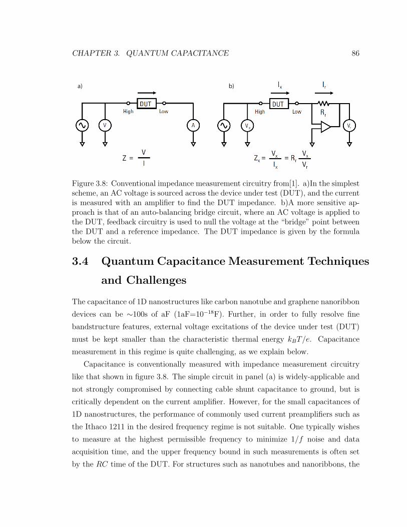
CHAPTER 3. QUANTUM CAPACITANCE 86
a) b)
Figure 3.8: Conventional impedance measurement circuitry from[1]. a)In the simplestscheme, an AC voltage is sourced across the device under test (DUT), and the currentis measured with an amplifier to find the DUT impedance. b)A more sensitive ap-proach is that of an auto-balancing bridge circuit, where an AC voltage is applied tothe DUT, feedback circuitry is used to null the voltage at the “bridge” point betweenthe DUT and a reference impedance. The DUT impedance is given by the formulabelow the circuit.
3.4 Quantum Capacitance Measurement Techniques
and Challenges
The capacitance of 1D nanostructures like carbon nanotube and graphene nanoribbon
devices can be ∼100s of aF (1aF=10−18F). Further, in order to fully resolve fine
bandstructure features, external voltage excitations of the device under test (DUT)
must be kept smaller than the characteristic thermal energy kBT/e. Capacitance
measurement in this regime is quite challenging, as we explain below.
Capacitance is conventionally measured with impedance measurement circuitry
like that shown in figure 3.8. The simple circuit in panel (a) is widely-applicable and
not strongly compromised by connecting cable shunt capacitance to ground, but is
critically dependent on the current amplifier. However, for the small capacitances of
1D nanostructures, the performance of commonly used current preamplifiers such as
the Ithaco 1211 in the desired frequency regime is not suitable. One typically wishes
to measure at the highest permissible frequency to minimize 1/f noise and data
acquisition time, and the upper frequency bound in such measurements is often set
by the RC time of the DUT. For structures such as nanotubes and nanoribbons, the

CHAPTER 3. QUANTUM CAPACITANCE 87
νDUT
CDUT
Cpar
νSENSE
CV meter
sense AMP
=+
CDUT
CDUT Cpar
νSENSE
νDUT
Figure 3.9: Parasitic cable capacitance in a typical capacitance test setup with a CVmeter. For small CDUT , the test signal is attenuated by a factor of ∼ CDUT/Cpar,which is on the order of 106 for typical nanostructures connected via standard coaxialcables. For νDUT ∼ kBT/e at 4K, this results in νsense <1nV.
desired measurement frequency is in the range of ∼10kHz, and the input impedances
of common amplifiers in this regime is no longer negligible as compared with the DUT
impedance.
The more sophisticated circuit shown in panel (b) of figure 3.8 is often employed
in instruments (such as the Andeen-Hagerling AH2700A discussed below) used to
measure capacitances approaching the aF regime[37, 44, 2]. Inevitably, connecting
such apparatus to a cryostat containing the DUT requires some length of cables that
have finite parasitic capacitance to ground on the order of hundreds of picofarads.
Such parasitic capacitance is manageable when the applied AC test signal is large, but
is unsuitable for the small test signals required to resolve features at cryogenic tem-
peratures. The diagram in figure 3.9 illustrates the problem. The extreme mismatch
between the DUT capacitance and the cable parasitic shunt produces an enormous
attenuation of the test signal, pushing even state-of-the art laboratory CV meters
beyond their resolution limits.
Finally, before discussing our approach to quantum capacitance measurements,
it is worth briefly mentioning two less conventional techniques. The circuit shown

CHAPTER 3. QUANTUM CAPACITANCE 88
a) b)
Figure 3.10: Other quantum capacitance measurement schemes. a)Penetrating elec-tric field measurement circuit employed by Eisenstein et al.[46] to measure 2D quan-tum capacitance. b)Resonant circuit configuration used by Ensslin et al.[29] for mea-suring the quantum capacitance of graphene.
in figure 3.10a has been employed by Eisenstein et al.[31] to measure the quantum
capacitance (compressibility) of 2DEGs as well as 2D graphene[46]. This approach
measures the penetrating electric field in the two-gate geometry discussed in the
previous section, and therefore is not applicable to 1D systems. The circuit shown
in figure 3.10b uses a frequency counter to determine the resonance frequency of an
LC circuit composed of the DUT, a reference inductor, and the connecting cables.
While such a circuit has been used recently by Ensslin et al.[29] to determine the
quantum capacitance of 2D graphene, the dependence on cable capacitance, and the
need for large applied excitation compared to temperature for suitable resolution
(20mV applied to DUT at T=1.7K for δC ∼170aF) also limit the usefulness of this
approach for capacitance measurements on 1D structures.
3.5 The Integrated Capacitance Bridge
To surmount the limitations discussed above for measuring the quantum capacitance
of 1D nanostructures, we constructed a capacitance bridge with amplifier and refer-
ence impedance wirebonded directly to the DUT, termed the “integrated capacitance
bridge” [85]. This approach is based on the work of Ashoori et al.[83] and is summa-
rized in figure 3.11. Essentially, parasitic capacitive shunting of the signal between
the DUT and the reference impedance is minimized by placing all critical components

CHAPTER 3. QUANTUM CAPACITANCE 89
CDUT
CparνSENSE
External ampli"erνDUT
Impedance-matching
ampli"er
Figure 3.11: The integrated capacitance bridge operating principle. The impedance-matching amplifier drives the large parasitic cable capacitance Cpar, preventing theshunting of the DUT signal νsense from the cables.
as close as possible to the DUT. The signal is extracted via an impedance-matching
amplifier, whose function is to drive the large parasitic cable capacitance and isolate
the DUT. The integrated bridge we discuss below achieves excellent capacitance res-
olution (60aF/√Hz at room temperature for a 10mV AC excitation at 17.5 kHz) for
test signals less than kBT/e down to temperatures of 4K, with amplifier output noise
of less than 10nV/√Hz
3.5.1 Amplifier and Bridge Circuit Design
The circuit model for the integrated bridge circuit is shown in figure 3.12. The circuit
consists of an impedance-matching amplifier, reference impedance, and the DUT
configured in a balance-bridge circuit, along with audio transformers for coupling AC
and DC signals into the circuit. The various circuit elements are discussed below.
Since we are interested in measurements across a broad temperature range down
to cryogenic temperatures, we use a GaAs-based high electron mobility transistor
(HEMT) as the impedance-matching amplifier[89]. A standard Si FET is unsuitable
due to carrier freeze-out at low temperature. The HEMT in our bridge is an un-
packaged (to minimize parasitic capacitance) FHX35X transistor manufactured by
the Fujitsu Corp, and has a wide (∼ 280µm) channel fabricated from epitaxially-
grown GaAs, with a gate capacitance ∼0.4pF. Several other commercially available
HEMTs, including the Agilent ATF 33143 and 34143, were found to be unsuitable in
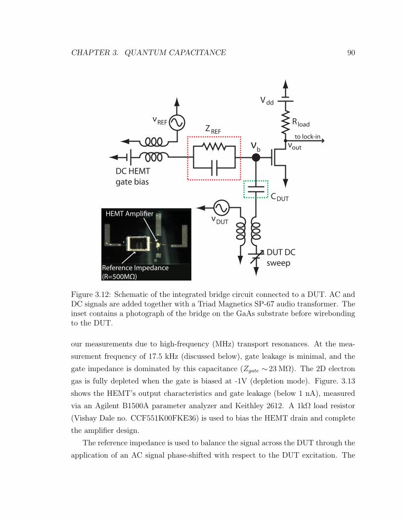
CHAPTER 3. QUANTUM CAPACITANCE 90
Z REF
R load
to lock-in
νREF
V dd
DC HEMT
gate bias
DUT DC
sweep
νb
HEMT Ampli!er
Reference Impedance
(R=500MΩ)
CDUT
νDUT
νout
Figure 3.12: Schematic of the integrated bridge circuit connected to a DUT. AC andDC signals are added together with a Triad Magnetics SP-67 audio transformer. Theinset contains a photograph of the bridge on the GaAs substrate before wirebondingto the DUT.
our measurements due to high-frequency (MHz) transport resonances. At the mea-
surement frequency of 17.5 kHz (discussed below), gate leakage is minimal, and the
gate impedance is dominated by this capacitance (Zgate ∼ 23 MΩ). The 2D electron
gas is fully depleted when the gate is biased at -1V (depletion mode). Figure. 3.13
shows the HEMT’s output characteristics and gate leakage (below 1 nA), measured
via an Agilent B1500A parameter analyzer and Keithley 2612. A 1kΩ load resistor
(Vishay Dale no. CCF551K00FKE36) is used to bias the HEMT drain and complete
the amplifier design.
The reference impedance is used to balance the signal across the DUT through the
application of an AC signal phase-shifted with respect to the DUT excitation. The

CHAPTER 3. QUANTUM CAPACITANCE 91
0 0.5 1 1.5V
ds [V]
0
10
20
30
40
I d [
mA
]
300K
77K
4K
0 0.5 1 1.5
Vds
[V]
I g [
A]
10−14
10−12
10−10
10−8
Figure 3.13: Output characteristics of Fujitsu FHX35X HEMT for Vgs = 0 at varioustemperatures. The inset shows the gate current Ig as a function of Vds for Vgs = 0(no load resistor). For temperatures 77K and below, the leakage is below 1pA.
AC impedance of the reference impedance should be chosen to be larger than the
HEMT gate AC impedance to prevent additional shunting of the DUT signal. As the
HEMT gate is DC biased through the reference (via a Yokogawa 7651 programmable
low-noise DC power supply), the reference DC impedance should ideally be at most
of the same order as the HEMT gate resistance across all temperatures. Additionally,
this reference impedance should have little variation with temperature to simplify
measurement calibration. To satisfy these constraints at the test frequency 17.5 kHz,
we use a 500 MΩ thick-film resistor (Tyco Electronics part no. 26M2248) with a low
thermal coefficient and a parasitic capacitance CREF ∼ 110fF. A photograph of the
assembled circuit before bonding to the DUT is given in the inset of figure 3.12.
3.5.2 Substrate Fabrication and Circuit Mounting
To avoid strain and thermal gradients at low temperature, a thermally-matched sub-
strate is required to mount the bridge circuit. We used a semi-insulating GaAs wafer
as the substrate (3” wafers from Wafertech Corp., diced into chips.), onto which a

CHAPTER 3. QUANTUM CAPACITANCE 92
Figure 3.14: Substrate fabrication process flow for the integrated capacitance bridge.The LOL 2000 lift-off and Shipley 3612 photoresist (PR) layers were deposited andprocessed according to the “Liftoff Processes” section of the Stanford Nanofabrica-tion Facility website (snf.stanford.edu/Process/Lithography/liftoff.html), resulting inrespective thicknesses of 200nm and 1.6µm.
23nm Al2O3 layer was grown via ALD (using a home-built setup) for additional elec-
trical isolation. Without this additional isolation, we found shunt impedances at room
temperature between the mounted circuit components with values ∼100s of MOhms.
Standard photolithography/liftoff processing were used to fabricate 300nm thick Al
electrodes for bonding. Al was chosen for its good adhesion, high conductivity, and
tendency to not form ohmic contact to the underlying GaAs[4, 96], which would also
shunt the circuit components. The substrate fabrication scheme is summarized in
figure 3.14. The substrates were next diced into 1.5cm×1.5cm chips, and the bridge
components were attached using thermally-conductive silver epoxy for the HEMT and
PMMA for the reference resistor. The bridge components were then wirebonded us-
ing Al wire, which was performed at OEpic Corporation (by Yi-Ching Pao and Diana
Fong) due to the fragile nature and small scale of the unpackaged HEMTs. Finally,
the assembled bridge circuit chips were attached to machined copper plates via copper

CHAPTER 3. QUANTUM CAPACITANCE 93
Table 3.1: Optimized HEMT bias conditions with corresponding amplifier outputsensitivity S and best achievable capacitance resolution (per root Hz) δC (measuredusing CDUT=250aF, before bonding graphene device to bridge).
T [K]Vdd[V] Vgs[mV] S[nV/
√Hz] HEMT Gain (νout
νb) δC [aF/
√Hz]
(νDUT =10mV rms)300 4 -50 8 0.047 6077 4 -50 7.4 0.063 594.2 4 -25 5.6 0.099 21
clips and silver epoxy for ease of handling and good thermal contact with the base of
the probe station into which the circuits were eventually placed for measurement.
3.5.3 Bridge Circuit Operation and Optimization
In operation, two phase-shifted AC signals, νDUT and νREF , are simultaneously ap-
plied to the DUT and reference resistor, respectively. The signal νb at the so-called
“bridge point” (figure 3.12) is an average of voltages at nearby circuit nodes, weighted
by the admittances of these nodes to the bridge point:
νb =YDUT
YΣ
νDUT +YREF
YΣ
νREF , (3.20)
where Y refers to the AC admittance and YΣ = YDUT + YREF + Ypar is the total
admittance seen from the bridge point. The “par” subscript refers to parasitic terms,
including the HEMT gate impedance. When balanced, i.e. νb = 0, the amplitude
and phase of the DUT impedance are given by
ZDUT =−νDUT
YREF · νREF
, (3.21)
independent of any parasitic capacitances. For a measurement of CDUT as a func-
tion of DUT DC gate voltage, the other circuit admittances in (3.20) need only be
characterized once, as other than CDUT they do not change with the gate voltage
sweep.
The HEMT amplifier is configured in the “common source” configuration, and the

CHAPTER 3. QUANTUM CAPACITANCE 94
0 5 10 15 2010
−8
10−7
10−6
10−5
Frequency [kHz]
PS
D [
V/
Hz
]√
fin
=17.5 kHz
DC Power [μW]
SN
R [
dB
]
400 600 800 100070
85
75
80
b)
a)
Figure 3.15: Noise performance of the integrated capacitance bridge. a) Integratedbridge output SNR as a function of DC power dissipation for a 1.5mV RMS inputsignal at room temperature. The symbols in the plot correspond to the following(Vgs[V ], Vdd[V ]) pairs: ∗ (-0.05,4), ⋆ (-0.1,4), (-0.15,4), (-0.1,5), ♦ (-0.05,5), (-0.15,5), (-0.1,6), × (-0.15,6), (-0.05,6). The optimal bias point, i.e. high SNRand low power, is marked by ∗. b) Output power spectral density (PSD) of the bridge(measured with a home-built spectrum analyzer) biased at the optimal bias point(-60 dB gain between bridge input and output) with 100µV RMS input signal). Theexcitation at 17.5kHz is indicated by the black circle.
DC gate bias and DC source-drain bias must first be optimized before operation. The
bias points for the HEMT are chosen to maximize SNR while keeping the DC power as
low as possible to avoid thermal drift and temperature gradients during measurement.
All measurements are performed in the dark to prevent optical excitation of the
exposed 2DEG in the HEMT.1 We found that the optimal bias point for the HEMT
is in the triode regime, which has low gain—even below 1 (Table 3.1)—but also
very low noise and thermal drift, and thus maximal SNR. The low HEMT gain is not
critical here, as it is compensated for by the high gain of the lock-in amplifier sampling
the HEMT output. Thus, the HEMT functions primarily as an impedance-matching
circuit element between the DUT impedance and the line impedance.
The measurement frequency of 17.5kHz was chosen because it is high enough to
for fast data acquisition and acceptable 1/f noise, and low enough so that the RC
charging time of the DUT can be ignored in the measurements. Figure 3.15 shows
1After cooling, HEMTs were temporarily exposed to light to enable navigating probes to thepads, so persistent photoconductivity may affect HEMT characteristics at 77K and 4K.
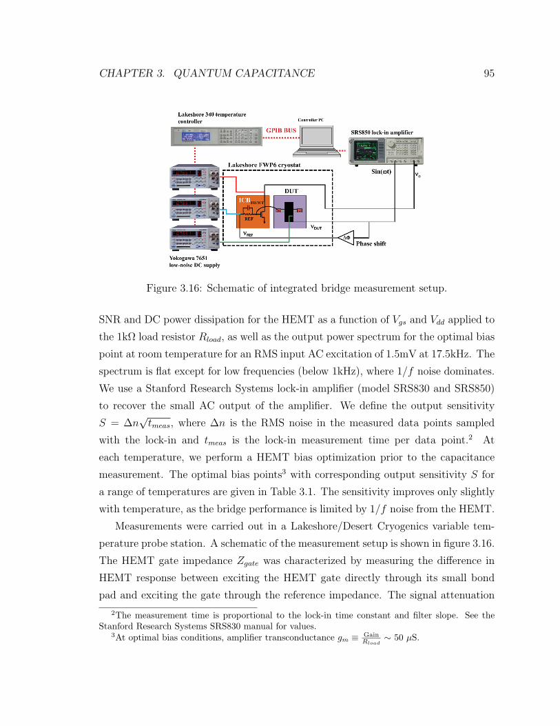
CHAPTER 3. QUANTUM CAPACITANCE 95
Figure 3.16: Schematic of integrated bridge measurement setup.
SNR and DC power dissipation for the HEMT as a function of Vgs and Vdd applied to
the 1kΩ load resistor Rload, as well as the output power spectrum for the optimal bias
point at room temperature for an RMS input AC excitation of 1.5mV at 17.5kHz. The
spectrum is flat except for low frequencies (below 1kHz), where 1/f noise dominates.
We use a Stanford Research Systems lock-in amplifier (model SRS830 and SRS850)
to recover the small AC output of the amplifier. We define the output sensitivity
S = ∆n√tmeas, where ∆n is the RMS noise in the measured data points sampled
with the lock-in and tmeas is the lock-in measurement time per data point.2 At
each temperature, we perform a HEMT bias optimization prior to the capacitance
measurement. The optimal bias points3 with corresponding output sensitivity S for
a range of temperatures are given in Table 3.1. The sensitivity improves only slightly
with temperature, as the bridge performance is limited by 1/f noise from the HEMT.
Measurements were carried out in a Lakeshore/Desert Cryogenics variable tem-
perature probe station. A schematic of the measurement setup is shown in figure 3.16.
The HEMT gate impedance Zgate was characterized by measuring the difference in
HEMT response between exciting the HEMT gate directly through its small bond
pad and exciting the gate through the reference impedance. The signal attenuation
2The measurement time is proportional to the lock-in time constant and filter slope. See theStanford Research Systems SRS830 manual for values.
3At optimal bias conditions, amplifier transconductance gm ≡ GainRload
∼ 50 µS.

CHAPTER 3. QUANTUM CAPACITANCE 96
0
200
400
600
800
1000
0
100
200
300
400
500300K4.2K
0 0.5 1 1.5 2|νREF ν |DUT/
Brid
ge
Ou
tpu
t [nV
]Bri
dg
e O
utp
ut
[nV
]
5 μm
Figure 3.17: Integrated bridge output as a function of |νREF/νDUT | for T=300K (leftaxis), with νDUT=8mV and phase difference between graphene DUT and REF signals∆Φ=144; and for T=4.2K (right axis), with νDUT=100µV and ∆Φ=155. The bridgeoutput minimum and phase difference ∆Φ are shifted slightly between the two curvesdue to changes in the REF and DUT impedances with temperature.
G is then related to the impedances by the equation G = Zgate
Zgate+ZREF. These complex
impedance values are used to calculate the relative phase between νREF and νDUT
required for balancing the bridge. Typical bridge balance curves are shown in figure
3.17 for a graphene DUT to be discussed below. The circuit is initially balanced
in this fashion at the onset of a CV measurement, using either an Agilent 81150A
function generator or Agilent 81110A pulse generator to phase-shift the applied AC
signals. The change in capacitance of the DUT as the gate DC bias is swept (also via
Yokogawa 7651 in our setup) is then calculated from the deviation of the bridge signal
νb away from the balance point using (3.20). Since the DC DUT impedance (graphene
gate impedance) is much larger (TΩ) than the other DC circuit impedances, the DC
HEMT gate bias does not vary during the CV measurement as the graphene DC gate
bias is swept. The measured capacitance change is therefore attributable to the DUT

CHAPTER 3. QUANTUM CAPACITANCE 97
capacitance. This approach allows for fast data acquisition, as the bridge does not
need to be balanced at every DUT gate voltage. The exact measurement protocol is
available from the Goldhaber-Gordon lab server or by request.
3.5.4 Measurement Noise
Our measurement goal is to obtain the maximal SNR in the extracted capacitance,
which we will define as:
SNR ≡ CavgDUT
δCDUT
=Y avgDUT
δYDUT
, (3.22)
where δYDUT is the noise in the measurement of YDUT . The “avg” superscript refers to
the fact that the individual samples of YDUT are averaged together to calculate SNR.
The signal νb at the bridge node is given by equation (3.20) above. The measure-
ment consists of sampling νb and then relating it to YDUT via (3.20). For notational
convenience, we define the inverse mapping: YDUT = f(νb). There will also be noise
δνb in the circuit at the bridge node, so that the measured signal at the bridge node
becomes νb → νb + δνb. For small noise levels, we then have:
YDUT + δYDUT = f(νb + δνb) ≈ f(νb) +∂f
∂νbδνb. (3.23)
We now see that the expression for SNR can be rewritten:
SNR =YDUT
δYDUT
=f(νb)∣∣∣ ∂f∂νb
∣∣∣ δνb . (3.24)
Maximizing the SNR is now equivalent to minimizing the partial derivative in the
denominator of (3.24). To make this more explicit, we define the sensitivity S:
S ≡∣∣∣∣ ∂νb∂YDUT
∣∣∣∣ , (3.25)

CHAPTER 3. QUANTUM CAPACITANCE 98
so that we have 1S
=∣∣∣ ∂f∂νb
∣∣∣. Now, we see that maximizing SNR is equivalent to
maximizing the sensitivity S. From (3.20), this sensitivity is simply:
S =
∣∣∣∣(νDUT − νREF )YREF + νDUTYpar
(YDUT + YREF + Ypar)2
∣∣∣∣ . (3.26)
Thus, the measurement sensitivity is maximized by increasing νDUT . However, in
practice, we limit this excitation to νDUT ∼ kBT/q to avoid blurring of density-of-
states features by our excitation as described above. This also prevents significant
thermal drift and heating. For measuring small capacitances associated with nanos-
tructures, the voltage νREF applied to the reference impedance typically needs to be
much smaller than the voltage νDUT applied to the DUT to balance the bridge, which
ensures that νREF is kept below kBT/q.
3.5.5 Characterizing Bridge Performance: Graphene Quan-
tum Capacitance Measurements
To demonstrate a practical application of our bridge, we measure the capacitance of
graphene with a strongly-coupled top gate. While such a 2D device doesn’t push the
limits of our measurement capabilities, it allows for an intermediate level (fF) gate-
tunable capacitance measurement that can be used to benchmark the performance of
the integrated bridge against the state-of-the-art commercial AH2700A bridge.
The graphene in our device was deposited on a SiO2/Si chip via mechanical ex-
foliation, and confirmed to be single-layer via optical contrast and confocal Raman
spectroscopy. 100nm of PMMA (A2, 950K MW) was spin-coated, and source/drain
leads to a selected graphene sheet were defined with e-beam lithography employing
local alignment with respect to a pre-defined metal alignment grid. Following Ti/Au
deposition (5/40 nm, respectively) and liftoff in acetone, the entire chip surface was
coated via e-beam evaporation with nominally 1.5 nm of Al, which then oxidized
almost immediately upon exposure to air. A top-gate electrode was patterned on top
of the graphene by e-beam lithography, followed by 40nm of e-beam evaporation of Al
and liftoff in acetone[76]. The active device area beneath the top gate was 14.85 µm2.

CHAPTER 3. QUANTUM CAPACITANCE 99
5 μm
Graphene
Top
Gate
Contact
Figure 3.18: Images of integrated bridge circuit with attached graphene DUT.a)Photograph of the integrated capacitance bridge and graphene DUT chip mountedon the copper plate. For scale, the graphene chip is 5mm×5mm in dimension. b)False-color AFM image of the measured graphene device. The graphene is colored blue,the source/drain contact is gold, and the top-gate is colored green.
The graphene device chip was finally wirebonded to the bridge chip, and both chips
were mounted on a copper support for thermal anchoring. An AFM image of the
device is shown in figure 3.18 alongside a photograph of the integrated capacitance
bridge and graphene DUT chip mounted on the copper plate.
Capacitance from bond pads, wirebonds, and probe tips contribute to the DUT
shunt capacitance, which is in parallel with CDUT and sets a constant baseline for
the measurement. We estimate this shunt capacitance to be no more than 10fF
based on capacitance measurements with the integrated bridge of semiconducting
nanotubes with similar device layout. Such materials posses a bandgap, and the
shunt capacitance can be measured by gating the DUT so that the Fermi level lies in
this gap, thus removing the contribution of the DUT to the measured capacitance.4
The measured shunt capacitance for the nanotube device and bridge was 850aF.
4For materials without a bandgap, the DUT capacitance can effectively be removed from thecircuit by attaching a large resistor in series with the DUT contacts so that the RC time constantof the DUT is much larger than the period of the DUT AC excitation.

CHAPTER 3. QUANTUM CAPACITANCE 100
−1 −0.9−0.8−0.7−0.6−0.5−0.4−0.3−0.2−0.1 0 0.1 0.2 0.3 0.4 0.5
−35
−30
−25
−20
−15
−10
−5
0
Top Gate Voltage (V)
Ba
ck G
ate
Vo
lta
ge
(V
)
0.04
0.06
0.08
0.1
0.12
0.14
0.16
0.18
0.2
−1
−0.5
0
0.5
−35
−30
−25
−20
−15
−10
−5
0
0.05
0.1
0.15
0.2
Top Gate Voltage (V)
Back Gate Voltage (V)
a) b)
Re
sis
tan
ce (h
/e2)
Re
sis
tan
ce (
h/e
2)
Figure 3.19: Resistance of a graphene device versus back gate and top gate voltagesat room temperature. The black line in (a) is a fit to the resistance peak associatedwith the Dirac/neutrality point in the graphene sandwiched between the top gateand back gate. The ratio of top gate coupling to back gate coupling decreases asthe temperature is lowered, likely due to thermal unequal thermal contraction ofthe dissimilar dielectrics. The relatively small resistance peak associated with thegraphene region underlapped by the top gate is a result this region’s comparativelysmall area (c.f. [47]).
The bond wires for the graphene device were somewhat longer, so we conservatively
allow for a shunt capacitance ten times larger. This is roughly 10% of the measured
capacitance (figure 3.20), so though the strength of our technique is in measuring
changes in capacitance with gate voltage, we can also obtain capacitance per unit
area to 10% accuracy. Our extracted value for geometric capacitance (capacitance far
from the Dirac point) is ∼7.5fF/µm2, consistent with dielectric thickness ∼10nm[76]5
and dielectric constant ∼8. These are plausible values for our oxidized Al dielectric,
though we do not have precise independent measures of the dielectric parameters
(figure 3.19).
2D Graphene has no energy gap between the conduction and valence bands. In-
stead, these bands meet at a point, termed the Dirac point, about which the energy-
momentum dispersion is linear. The density of states and associated quantum capac-
itance CQ therefore vary linearly with energy near the Dirac point. As the top-gate
bias voltage is swept, the Fermi level scans the graphene energy spectrum, passing
5We note that while this thickness is consistent with other work[76], the value is unexpectedlythick, since the evaporated Al thickness before oxidation is only ∼1.5nm.

CHAPTER 3. QUANTUM CAPACITANCE 101
0 0.5 1 1.580
90
100
110
120
Ca
pa
cita
nce
[fF
]
V [V]g
T=300K ( =8mV)ν DUT
T=77K ( =130μV)ν DUT
Figure 3.20: CV curves for top-gated graphene device measured with the integratedcapacitance bridge. The gate voltage dependence is a direct result of the graphenedensity of states. At room temperature, using an 8mV DUT excitation, the noise perdata point is ∼11aF. At 77K, the Dirac point is more cleanly resolved while using asmall DUT excitation of 130µV, with a noise level ∼53aF.
through the Dirac point, where the capacitance reaches a minimum. This minimum
capacitance is limited by the temperature, disorder, and parasitic capacitance[76].
For top-gate voltages that tune the Fermi level far in energy from the Dirac point,
the density of states and associated CQ are large, so that Cox will dominate, resulting
in a C-V curve that saturates at large positive and negative gate voltages. Simulations
of the quantum capacitance of graphene are discussed in appendix D.
Figure 3.20 shows graphene capacitance measurements for our integrated bridge
at both room temperature and 77K. At room temperature, using an AC excitation
of 8mV for νDUT , the overall capacitance curve matches the trend expected for a
quantum capacitance proportional to the density of states of graphene (measured

CHAPTER 3. QUANTUM CAPACITANCE 102
resolution δC ∼11aF)6, and agrees with existing graphene capacitance measurements
in the literature[76, 99, 13, 29]. The capacitance is symmetric about the Dirac point,
which occurs at a top gate voltage Vg ∼0.5V. At 77K, a substantially lower excitation
of 130µV was used for νDUT (peak-to-peak amplitude ∼ 118kBT/q). The capacitance
curve is again cleanly resolved (measured resolution δC ∼53aF), with improvement
in the sharpness of the capacitance around the Dirac point due to lower temperature
and excitation (depth of Dirac point capacitance dip ∆C increased from ∼15fF to
∼21fF).
Upon direct comparison with the commercial AH2700A Andeen-Hagerling AH2700A
Ultra-precision Capacitance/Loss Bridge, which represents the state-of-the-art for
precision capacitance measurement tools, the resolution of our integrated bridge ex-
ceeded the resolution of the commercial tool by several orders of magnitude using
comparable data acquisition time. These comparative measurements were performed
on exactly the same graphene devices, which were left bonded to the integrated bridge
circuitry to avoid perturbing the DUT. However, this circuitry was powered down,
and probes driven by the AH2700A directly contacted pads attached to the graphene
and its gate, bypassing the integrated bridge circuitry and isolating the capacitance of
the graphene device. The shunt capacitance of the integrated bridge (∼10fF) should
not have effected the noise in the AH2700A’s capacitance measurements–indeed, the
AH2700A performed to its manufacturer’s specifications for noise. Further, the ac-
quisition time for each data point (∼30s) was approximately equal for both the
integrated bridge and the AH2700A measurements, allowing for direct comparison
between curves.7
Figures 3.21a,b show graphene capacitance measurements for both our integrated
bridge and the AH2700A at room temperature and 77K, respectively. At room tem-
perature, with an AC excitation of 8mV for νDUT , the overall capacitance curves
match for the two measurements, though our integrated bridge is significantly less
noisy (δC for the integrated bridge is ∼11aF; for the AH2700A, δC ∼675aF). At 77K,
6The measurements were acquired with the lock-in low pass filter set to 24dB/oct rolloff and a3s time constant, corresponding to 38.4s of acquisition per data point.
7Note that this per-point acquisition time contains settling times as well as wait times associatedwith polling the GPIB bus.

CHAPTER 3. QUANTUM CAPACITANCE 103
0 0.5 1 1.580
90
100
110
120
Ca
pa
cita
nce
[fF
]
V [V]g
Ca
pa
cita
nce
[fF
]
a)
b)
T=300K
T=77K
AH2700A ( =4mV)ν DUT
Integrated Bridge ( =130μV)ν DUT
AH2700A ( =8mV)ν DUT
Integrated Bridge ( =8mV)ν DUT100
110
120
130
140
0 0.5 1 1.5V [V]g
Figure 3.21: Comparison of measured CV curves for top-gated graphene device forthe AH2700A and the integrated bridge. Acquisition time for all measurements washeld constant (∼30s per point) to enable direct comparisons between measurements.a) At room temperature using an 8mV DUT excitation, noise in the integrated bridgemeasurement is ∼11aF, while the noise for the commercial bridge is ∼675aF. b) At77K, the smallest possible DUT excitation allowable by the tool of 4mV was usedfor the commercial bridge measurement, and the Dirac point is poorly resolved dueto the high noise level ∼5000aF. For the integrated bridge measurement, the Diracpoint is cleanly resolved while using a small DUT excitation of 130µV, with a noiselevel ∼53aF.

CHAPTER 3. QUANTUM CAPACITANCE 104
the minimum excitation allowed by the commercial tool of 4mV was used for νDUT for
the AH2700A measurements (peak-to-peak amplitude ∼ kBT ), while a substantially
lower excitation of 130µV was used for νDUT for the integrated bridge measurements
(peak-to-peak amplitude ∼ kBT/18). The capacitance curve is cleanly resolved for
the integrated bridge measurements (δC ∼53aF), with improvement in the sharp-
ness of the capacitance around the Dirac point due to both lower temeprature and
excitation, whereas these features are obscured by the excessive noise level for the
AH2700A measurements (δC ∼5000aF). At 77K, our integrated bridge SNR is 100
times that of the commercial bridge. Thus, for comparable resolution, the integrated
bridge enables measurements 10,000 faster than the commercial tool.
3.5.6 Summary of the Integrated Capacitance Bridge
We have demonstrated a reliable method for integrated high-resolution quantum ca-
pacitance measurements over a wide temperature range using an integrated bridge
circuit directly wirebonded to the DUT. The performance of our bridge was tested
by measuring the capacitance of a top-gated graphene device, illustrating directly
how the integrated bridge enables the fast measurement of quantum capacitance for
nanostructures down to cryogenic temperatures, and achieves 10s of attofarad reso-
lution per root hertz at room temperature (equivalently, ∼4 e− per root hertz on the
DUT) while limiting the excitation amplitude to below kBT/q.
3.6 Future Directions
We close this chapter with a discussion of the ongoing experimental efforts to utilize
the integrated capacitance bridge as a probe of 1D nanostructures. As described
above, we intend to use the bridge to investigate multiple subband occupation in
graphene nanoribbons and characterize the mobility of individual carbon nanotubes.
Figure 3.22 shows a micrograph of a preliminary top-gated carbon nanotube de-
vice and a photograph of the device with capacitance bridge in the measurement

CHAPTER 3. QUANTUM CAPACITANCE 105
Figure 3.22: Photograph of top-gated nanotube device with capacitance bridge inprobestation and scanning electron micrograph of nanotube device. There is a layer ofKapton tape between the nanotube chip and the copper substrate plate to electricallyisolate the nanotube back gate. The backgate is connected via a wirebond to a stripof copper tape, also electrically isolated with Kapton tape. A thin wire has beensoldered to this copper tape so that voltage can be applied to the nanotube back gatewithout the use of a probe. The copper substrate plate also holds a second pair ofnanotube/capacitance bridge chips as shown in the photograph.
probestation. Nanotubes were grown via chemical vapor deposition on quartz sub-
strates and transferred to silicon wafers for device fabrication as outlined in [72].
Ti/Pd contacts and Ti/Au bond pads were deposited via e-beam lithography and
evaporation, and ALD was used to grow ∼10nm of alumina as the gate dielectric.
Figure 3.23 shows initial capacitance data from integrated bridge measurements
of the nanotube device as a function of back gate voltage. By tuning the gate voltages
appropriately, the nanotube section beneath the top gate can be electrically isolated
from the contacts by gating the outer regions of the nanotube into the bad gap.
Capacitance measured in this regime reflects the shunt capacitance between the probe
tips and wirebonds.8 As the gate voltages are further tuned and the outer segments
of the nanotube are gated into either the conduction or valence band, the measured
capacitance will abruptly jump, signifying the occupation of the channel with charge
8In general, this shunting can be reduced substantially[88] by placing a grounded copper shieldingplane above the device and between the probes, though no such shield was used in these measure-ments.

CHAPTER 3. QUANTUM CAPACITANCE 106
CON
COFF
CNT
Figure 3.23: Preliminary capacitance data of an individual top-gated carbon nanotubemeasured via the integrated capacitance bridge. The nanotube channel is gated off(COFF ) at the most positive back gate voltages. For increasingly negative voltages,the hole channel is populated CON), with CNT = CON − COFF . Data were takenat room temperature with an AC excitation of 15mV and a capacitance resolutionδC ∼13aF.
carriers. The value of the capacitance in this regime is then the sum of the shunt
capacitance and the nanotube total capacitance. The data in the figure illustrate this
capacitance trend. At the most positive back gate voltages, the nanotube channel is
depleted (COFF ). As the gate voltage moves to more negative values, the hole channel
is populated, and the capacitance sharply jumps to the value CON . The difference
between these values is a measure of the total nanotube capacitance, including its
quantum capacitance.
In addition to measurements on 1D nanostructures, there are also efforts underway
toward performing capacitance measurements on topological insulators (Bi2Se3) and
complex oxides, systems that have enjoyed much recent excitement in the condensed
matter physics community.

Chapter 4
Transport Across Tunnel Barriers
in 1D
4.1 Introduction
In this final chapter, we discuss how interacting systems of fermions in 1D are funda-
mentally different from higher dimensional systems, and propose a set of 1D tunneling
measurements in carbon nanotubes to probe these interactions. We then present two
fabrication schemes for creating the nanotube devices needed for such measurements,
one using a scalable, global alignment procedure, and the other using a local align-
ment procedure. Finally, we highlight the significant technological hurdles limiting
the proposed measurements, and discuss avenues for future measurements.
4.2 The Failure of Fermi Liquid Theory in 1D
Electron flow in higher dimensional systems (2D and 3D) is successfully described by
Landau Fermi liquid theory[60], in which there exists a one-to-one correspondence
between non-interacting and interacting electron states (quasiparticle excitations).
In these systems, the important electron scattering processes occur around the Fermi
level, significantly simplifying quantitative analysis (4.1a,b). The approximations of
Landau Fermi liquid theory are correct when the electronelectron relaxation time τee
107

CHAPTER 4. TRANSPORT ACROSS TUNNEL BARRIERS IN 1D 108
Figure 4.1: Failure of Fermi liquid theory for 1D electron gas, adapted from [40]. InFermi liquid theory for three-dimensional systems, (a) single electron energy levelsand (b) interacting electron energy levels exhibit a one-to-one correspondence; quasi-particle excitations behave as nearly free particles (i.e., the particles can “move pasteach other”). (c) Such a description is not valid in a 1D electron system, since thenature of electron−electron scattering changes. The reduced dimensionality preventselectrons from moving past each other, and only collective excitations may exist

CHAPTER 4. TRANSPORT ACROSS TUNNEL BARRIERS IN 1D 109
E (q)
q0 2kF
E (q)
q0 2kF
a) b)
E
k
Figure 4.2: Particle-hole excitations in different dimensions, adapted from [40]. a)Excitations of energy E(q) as a function of momentum q in higher dimensional systems(2D and 3D). Excitations exist down to zero energy for all momenta between q = 0and q = 2kF . This is because electrons can be excited from just below the Fermisurface to just above, as shown below the graph. b) Excitations in 1D. At zeroenergy, only excitations at k = 0 and k = 2kF exist, as shown below the graph,leading to well-defined states at low energy.
is much larger than both the relaxation times for scattering of electrons with phonons
and impurities, τe−ph and τe−imp respectively. Essentially, quasiparticle excitations in
higher dimensional systems behave as nearly free particles (i.e., the particles can move
past each other). However, the Landau Fermi liquid theory description of many-body
systems is not valid for interacting systems in 1D. The restricted dimensionality in 1D
changes the nature of electronelectron scattering so that only collective excitations
exist in interacting systems, as illustrated in figure 4.1c.

CHAPTER 4. TRANSPORT ACROSS TUNNEL BARRIERS IN 1D 110
Figure 4.3: Bosonization of 1D fermions[79]. For low energy excitations, the single-particle spectrum can be linearized around the Fermi level, shown in the left panel.The degeneracy g(M) of an excitation of energy M∆ for this linearized spectrum isshown in the right panel. Such excitations have a “bosonic” character, illustrated bythe form of the partition function.
4.2.1 Luttinger Liquids
The theoretical description of the interacting 1D quantum state, first developed by
Tomonaga and Luttinger, involves plasmon-like excitations that behave as bosons.
This can be seen by considering the allowed excitation diagram in figure 4.2. In
higher dimensional systems (2D and 3D), Excitations of a specific energy have a
poorly defined momentum as the energy goes to zero. This is because and excitation
of arbitrarily low energy can be created at any momentum from q = 0 to q = 2kF
by simply raising an electron from just below the Fermi surface to just above at any
points on the surface. However, in 1D, as the excitation energy approaches zero,
only excitations near either q = 0 or q = 2kF exist. This leads to excitations of
increasingly well-defined momenta as the energy tends to zero. These particle-hole
excitations can be interpreted as well-defined particles in 1D, just as quasiparticles
are well-defined in higher-dimensional Fermi liquids. However, unlike quasiparticles,
these particles are bosons, since they consist of excitations of pairs of fermions. To
see this “bosonization” more quantitatively, consider the diagrams in figure 4.3. For
low energy excitations, we can linearize a generic 1D dispersion around the Fermi
level:
εn ≈ εF +M∆, (4.1)

CHAPTER 4. TRANSPORT ACROSS TUNNEL BARRIERS IN 1D 111
where ∆ = ℏνF πL
is the single-particle energy level spacing, M ∈ Z+, νF is the Fermi
velocity, and L is the length of the system. We now examine the possible excitations
of this linearized fermion dispersion. For an excited state of energy E = E0 +M∆,
with M = 4, the degeneracy g(M) = 5, as shown in the diagram. Analyzing the
degeneracy for all M leads to the partition function:
Z = e−βE0
∞∏ℓ=1
1
1− e−ℓβ∆, (4.2)
where again ℓ ∈ Z+. This is the partition function for an equivalent system of massless
bosons with the dispersion:
ℓ∆ = ℏνFkℓ, (4.3)
where kℓ =ℓπL
is the boson momentum. A highly correlated quantum state emerges
from this analysis, which, for an excitation of energy M∆ of the N -particle Fermi sea
| F (N)⟩, is described by the bosonic basis states mℓ:
| mℓ⟩ =∏ℓ
1√mℓ
(b†ℓ)mℓ | F (N)⟩, (4.4)
with bosonic creation operators : b†ℓ ≡1√ℓ
∞∑n=1
c†n+ℓcn,
where the c†n are the common fermion creation operators. The positive integers mℓ
define the g(M) partitions for the excitation, subject to the constraint∑M
ℓ=1 ℓmℓ =
M [79].
When interactions are added, this correlated many-electron state is termed a Lut-
tinger liquid, and is characterized by the parameter:
α =1
2ℏ4
(ν(0)
2πνF
), (4.5)
where ν(k) = f [Vee(r)], Vee(r) is the electron−electron interaction potential, and
ν(0) = ν(kF ). This parameter α clearly reflects the strength of the electron−electron
interactions.

CHAPTER 4. TRANSPORT ACROSS TUNNEL BARRIERS IN 1D 112
Source Drain
Narrow gate
Dielectric
b)
a)
1D channel
Source Drain
Fermi Liquid (quasiparticles)
Luttinger Liquid (spinons and holons)
Figure 4.4: Transport through a Luttinger liquid and proposed measurement scheme.a) Two-terminal conductance of a 1D channel. Quasiparticle excitations in the Fermiliquid source decompose into spin and charge excitations in the 1D channel, thenrecombine into quasiparticles in the Fermi liquid drain. Such a measurement is notsensitive to interactions. b) Cross-section schematic of proposed nanotube tunnelingdevice. A narrow top-gate is used to create a sharp, tunable tunnel barrier inside ananotube, isolating regions of the Luttinger liquid. Conductance measured across thetunnel barrier is sensitive to the strength of the interactions.
4.3 Probing Interactions in 1D: Tunneling
One might intuitively expect the two-terminal conductance of a ballistic 1D device
to strongly depend on the strength of the interactions. However, this is not the case.
Consider the simplified device structure in figure 4.4a, where charge is injected from
the source, through a 1D channel, and into the drain. Quasiparticle excitations in the
higher-dimensional Fermi liquid source decompose into Luttinger liquid excitations
(spinons and holons) in the 1D region, then recombine into quasiparticles in the
Fermi liquid drain. If conductance is only measured between the Fermi liquid source
and drain contacts, the measurement is not sensitive to the 1D interactions, and the

CHAPTER 4. TRANSPORT ACROSS TUNNEL BARRIERS IN 1D 113
a)
Figure 4.5: Previous nanotube tunneling measurements. a) Conductance of varioussegments of a nanotube from [103]. Transport across segments I and II, which containno kink (τ ∼ 1), is enhanced comparison to transport across the kinked segment(τ ∼ 0). b) AFM image of the device measured in (a) with visible kink.
standard quantized conductance discussed in chapter 1 is measured.
In contrast to the simple conductance measurement described above, a 1D tun-
neling measurement is sensitive to interactions. For a Luttinger liquid, the tunneling
density of states ρ has a power law behavior ρ ∼ ρ(µ − ϵ)α as a function of energy
ϵ. This leads to power law behavior of conductance G across a tunnel barrier as a
function of temperature and bias voltage:
G =dI
dV∼
Tα, eV ≪ kBT linear regime
V α, eV ≫ kBT high bias regime.(4.6)
4.3.1 Tunneling Across Barriers in Carbon Nanotubes
Carbon nanotubes have attracted significant interest for studying electronic properties
of 1D electron systems[10, 103, 9, 52, 51], and as predicted theoretically, have been
shown to exhibit Luttinger liquid behavior in tunneling transport measurements.
Previous experimental efforts include tunneling between two Luttinger liquids in a
kinked nanotube system. Figure 4.5 summarizes the results. In these experiments,
only the extreme cases of no tunnel barrier and strong tunnel barrier were studied.
CHAPTER 4. TRANSPORT ACROSS TUNNEL BARRIERS IN 1D 114
Additionally, the onset of Coulomb blockade due to poorly transmitting contacts
prevented Luttinger liquid measurements at very low temperatures, which we discuss
in section 4.5.2 below. Experimental questions remain about how the conductance
behaves in the other tunneling regimes and at lower temperatures.
We propose to extend these studies by using narrow top gates to introduce tun-
able tunnel barriers within nanotubes. Figure 4.4b shows a schematic of the pro-
posed device. Although Luttinger liquid behavior has only been previously observed
via transport measurements in metallic nanotubes, Luttinger liquid behavior may be
expected in both metallic and semiconducting nanotubes. The Luttinger liquid may
emerge in any 1D electronic system where the electronic band structure can be lin-
earized around the Fermi level; the presence of a band gap would not change this as
long as the Fermi level lies above the gap (which is the case for the gated nanotube).
By measuring the conductance G between the source and drain contacts as a func-
tion of narrow gate voltage, tunneling between Luttinger liquids in various regimes
of barrier transmission should allow the quantitative measurement of the strength of
electron−electron interactions.
4.4 Device Fabrication
To create the nanotube tunneling devices, we explored two different fabrication ap-
proaches, global alignment and local alignment, which we now describe.
4.4.1 Global Alignment
We first explored a global alignment approach, which relies on the probabilistic place-
ment of the nanotubes using lithographically defined catalyst fields. This probabilistic
approach allows us to pre-define regions in which carbon nanotubes will grow, and
therefore fabricate many top-gated devices at once. Such a scalable approach had not
been used before for fabrication of carbon nanotube devices with several top gates[84].
Specifically, the global process uses multiple steps of electron-beam (e-beam) lithog-
raphy aligned with respect to global alignment marks on the edges of the chip to

CHAPTER 4. TRANSPORT ACROSS TUNNEL BARRIERS IN 1D 115
Figure 4.6: Process flow for global alignment fabrication of carbon nanotube top-gated transistors.
create hundreds of potential single-walled carbon nanotube (SWNT) transistors with
source-drain spacings down to 200nm and with sub-30nm metal top gates for creat-
ing tunable tunnel barriers. Probabilistically, some fraction of the finished devices
is then expected to contain nanotubes in the correct position, which is verified by
conductance measurements in a probe stations. Figure 4.6 shows the steps used in
the fabrication of the nanotube chips. The substrate used for fabrication is a degener-
ately doped Si substrate with 100nm-1µm thick thermally grown SiO2 film. < 001 >
crystal orientation is used for ease of cleaving, and resistivity is less than 0.005 Ω−cm
to prevent carrier freeze out at cryogenic temperature so that the Si can be used as
a back gate. A Leica VB6 e-beam tool was used for the aligned lithographic steps in
the fabrication. The typical alignment achieved was 1520nm for 3σ error. In the first
step, alignment marks were lithographically defined in PMMA resist, then transferred

CHAPTER 4. TRANSPORT ACROSS TUNNEL BARRIERS IN 1D 116
Figure 4.7: Nanotube transistors fabricated using global alignment.
by CHF3-based reactive ion etching into the SiO2 film. These alignment marks were
then used in all subsequent lithography steps. Following alignment mark definition,
catalyst regions were defined for individual devices, and lifted off iron oxide/alumina
catalyst material solution in methanol, as described. Each individual SWNT device
employs two 4µm×4µm catalyst regions separated by 7 µm. After iron oxide/alumina
catalyst regions were defined, SWNTs were grown in a tube furnace via chemical va-
por deposition. The catalyst deposition and growth are described in appendix B. The
catalyst regions on the SWNT chips were intentionally positioned in the growth fur-
nace so that the gas flow direction was parallel with the line connecting two catalyst
marks. Following SWNT growth, e-beam lithography with alignment, followed by
e-beam evaporation and lift-off of Pd were used to define 40nm thick Pd low Schot-
tky barrier (ohmic) contacts to the nanotubes. The spacing between contacts, which
defined the length of the active region of the carbon nanotube, varied between 200
nm and 5µm. These channel lengths were chosen to compromise between finite-size
effects and the probability of point defects in the nanotubes. After Pd ohmic contacts
were defined, Ti(10 nm)/Au(35 nm) large area source and drain contacts were lifted
off and aligned to Pd contacts. The devices were then annealed in Ar at 220 C for
10 min to improve the contact resistance. Prior to definition of narrow top gates, a

CHAPTER 4. TRANSPORT ACROSS TUNNEL BARRIERS IN 1D 117
Back gate voltage (V)
Top
ga
te v
olt
ag
e (
V) C
on
du
cta
nce
(e /h
)2
a) b)
Figure 4.8: Global alignment nanotube device transport. a) Room temperature con-ductance versus back-gate voltage of a representative device with channel length of500nm. The device has highly transmitting contacts and can be fully depleted. b)T=4K characterization of device conductance as a function of back gate and top gate.The diagonal features suggest the top gate only couples globally to the underlyingnanotube, not locally.
630nmthick alumina layer was deposited by atomic layer deposition (ALD) to isolate
the electrically contacted nanotube. Finally, e-beam lithography with alignment and
lift-off processing was used to define 20 nm wide Ti(5 nm)/Au(20 nm) nanowire gates
between the region defined by Pd contacts. One of the final device structures is shown
in figure 4.7.
Figure 4.8a shows a room temperature conductance trace as a function of the
back-gate voltage (applied to the bulk of the conductive silicon substrate) for a rep-
resentative global alignment device. The contacts are highly transmitting, and the
device can be fully depleted, suggesting a semiconducting SWNT spanning the chan-
nel. However, conductance measurements down to T =4K as a function of top-gate
voltage and back gate voltage suggest that the top gate does not locally electrostat-
ically couple to the nanotube, but instead couples to the entire channel (for channel
lengths down to 200 nm), as shown in figure 4.8b. This is likely due either to a top
gate electrode that does not span the entire channel, or device thicknesses (dielectric
thickness, channel length, gate width) that are not optimized. In general, the yield
of global alignment devices with suitable parameters for tunneling measurements was

CHAPTER 4. TRANSPORT ACROSS TUNNEL BARRIERS IN 1D 118
Figure 4.9: Nanotube device fabricated via local alignment methods. The im-age shows a false color SEM micrograph of a nanotube (red) spanning contacts(green)with two top gates (purple).
too low to pursue this approach.
4.4.2 Local Alignment
To achieve suitable device yield, we turned to a more conventional local alignment
fabrication approach[10]. After nanotube growth from catalyst regions described
above, a local alignment grid is deposited. Next, an atomic force microscope (AFM)
is used to image candidate nanotubes with respect to the local alignment marks,
and uniquely tailored lithography patterns are created for each candidate nanotube
device in a similar fashion to the graphene device fabrication described in chapter 3.
The rest of the device fabrication proceeds in the same manner as with the global
alignment scheme, except an FEI XL-30 SEM with Nabity pattern generator was used
for the local alignment e-beam lithography. The clear downside of this approach is a
more labor intensive fabrication process that potentially introduces defects into the
nanotubes, since they must be imaged at intermediate fabrication steps. However, the
device yield is much greater, with nearly all fabricated devices containing functional
local top gates. Figure 4.9 shows a representative device fabricated via local alignment
with two top gates.
Transport measurements shown in figure 4.10 highlight the functioning local top

CHAPTER 4. TRANSPORT ACROSS TUNNEL BARRIERS IN 1D 119
2 (V)
a) b)
Figure 4.10: Local gating in top-gated nanotubes at T=4K. a) 2D conductance mapof nanotube as a function of back gate and one top gate voltage. The slope of thedashed guide to the eye is proportional to the ratio of the gate capacitances. b) 2Dconductance map of nanotube device as a function of two top gate voltages. Thevertical/horizontal slopes of the features indicate that the gates couple only locallyto the nanotube segments directly beneath them.
gates obtained with local alignment fabrication. In 4.10a, the conductance is plotted
as a function of both the back gate voltage and one of the top gate voltages. The region
under the top gate is gated by both the top gate and the back gate, as indicated by the
sloped features marked by the dashed line. The slope of this line is proportional to the
ratio of top gate to back gate capacitance, and agrees well with the expected ratio ∼30
expected from the device geometry. Figure 4.10b shows the device conductance as a
function of both top gate voltages at a fixed back gate voltage. Here, the conducting
region is bounded by completely vertical and horizontal lines, indicating that each top
gate couples only locally to the underlying nanotube, with negligible cross-coupling.
4.5 Device Phenomenology and Limitations
Although we have successfully created nanotube devices with local top gates, the
utility of the devices is limited by the formation of Schottky barriers and disorder.
Figure 4.11a shows the conductance of a nanotube device as a function of back gate
voltage at T =4K. The conductance trace is separated into three distinct regions,

CHAPTER 4. TRANSPORT ACROSS TUNNEL BARRIERS IN 1D 120
Conduct
ance
(e
2/h
)
Conducta
nce (e
2/h)
Conducta
nce (e
2/h)
Conducta
nce (lo
g s
cale
)
Back Gate Voltage (V)
Back Gate Voltage (V)
Back Gate Voltage (V)
a)
b)
c)
d)
Fabry-Perot
Transition
Coulomb Blockade
Figure 4.11: Conductance of nanotube device in various regimes. a) Zero-bias conduc-tance vs. back gate with various conductance regimes circled. b) Fabry-Perot regime.Phase coherent scattering dominates transport in this regime, which is seen in inter-ference pattern in the 2D conductance map. c) Transition regime. In this regime,the conductance transitions in a non-trivial way from Fabry-Perot conductance toCoulomb blockade. d) Coulomb blockade regime. Here, the transport displays thecharacteristic Coulomb blockade diamond pattern.

CHAPTER 4. TRANSPORT ACROSS TUNNEL BARRIERS IN 1D 121
which we describe below.
4.5.1 Fabry-Perot Regime
For large, negative gate voltages, the contacts are the most transmitting, and the
electrical connection between the hole-channel of the nanotube and the Pd contact
metal has a strongly reduced Schottky barrier as compared with the electron-channel.
Still, transmission through the contacts is not perfect, and injected charges will scatter
between them before exiting the device. At low temperature, transport becomes phase
coherent, and this scattering leads to the interference pattern shown in figure 4.11b.
This pattern is nicely described by a model that is analogous to the familiar Fabry-
Perot optical interferometer[65]. As the gate voltage is swept, the energy of the Fermi
level with respect to the bottom of the subband (or neutrality point in a metallic
nanotube) is changed, and the wavevector of the injected carriers is correspondingly
modulated. The wavevector is similarly modulated by changing the source-drain
bias voltage. Phase is accumulated as carriers traverse the nanotube, and when the
round-trip phase shifts by 2π as a function of gate or bias voltage, the conductance
undergoes an oscillation. The energy scale δEFP of these oscillations is found by
setting the round-trip phase shift equal to 2π:
2LeδEFP
ℏνF= 2π. (4.7)
Such strong conductance modulations occur at other interfaces within these devices,
including the interfaces between regions with and without an ALD dielectric coating.
These modulations will therefore exist in any tunneling measurement data, compli-
cating their interpretation.
4.5.2 Coulomb Blockade Regime
As the gate voltage is increased to more positive vales, the Fermi level moves into
the nanotube band gap, indicated by the zero conductance region in 4.11a. Just
before the band gap region, the nanotube is in the “Coulomb blockade” regime, where

CHAPTER 4. TRANSPORT ACROSS TUNNEL BARRIERS IN 1D 122
single-electron charging dominates the conductance. The characteristic diamond-like
Coulomb blockade features are shown in 4.11d. In this regime, the Schottky barriers
to the nanotube are substantial, and transmission through the contacts is greatly
reduced: τ ≪ 1, creating a quantum dot.
In chapter 2, we tacitly assumed that the electron wavefunctions in the 1D chan-
nel of interest were well-coupled to the contacts, and that the number of electrons
in the channel could be continuously varied. This is no longer valid in the Coulomb
blockade regime, where we require the number of electrons on the nanotube quan-
tum dot to be an integer. We can quantify the onset of single-electron tunneling by
considering the ratio of two parameters, the nanotube level spacing ∆ε and the level
width/broadening Γ. The nanotube structure (chirality, length, diameter) defines ∆ε,
and the strength of the tunnel barriers at the contacts defines Γ, as more strongly
coupled contacts to the nanotube will result in broader nanotube energy levels. The
quantum dot energy level “escape” rate is then ∼ Γ/ℏ. Disregarding Coulomb block-
ade for a moment, an applied bias V will inject eV/∆ε charges into the dot, resulting
in the dimensionless conductance1 Γ/∆ε. Single-electron tunneling can occur when
the system’s energy levels are spaced further than the level width, so that the energy
levels can be separately populated with a well-defined, integral number of carriers.
The following restriction therefore must be satisfied to observe Coulomb blockade[42]:
Γ
∆ε≪ 1. (4.8)
The analysis from chapter 2 is otherwise still correct for a nanotube quantum
dot, so that we can still apply (2.6) and (2.9), now of course with the important
change that the number of charges N is an integer. These formulas can be used to
generate the diamond pattern in figure 4.11d, though it is instructive to analyze the
underlying physics a bit further. At zero bias, the conductance through the nanotube
quantum dot will be zero unless the gate voltage tunes a single-particle level to align
energetically with the chemical potential of the leads. Consider the situation where
1This dimensionless conductance is known as the Thouless conductance: gth ≡ Γ∆ε , which char-
acterizes the onset of Anderson localization. For a disordered, open quantum system, Andersonlocalization occurs when gth < 1[86].

CHAPTER 4. TRANSPORT ACROSS TUNNEL BARRIERS IN 1D 123
the gate is tuned to the precise voltage V ⋆g where the N−th charge tunnels onto the
nanotube. To add the next charge, we must then satisfy the relation:
e2
Cg
(N + 1) + ε(N) + ∆ε− eV ⋆g − e∆Vg = 0, (4.9)
where ∆Vg is the required change in gate voltage. Simplifying using (2.6), we find:
∆Vg =e2
Cg
+∆ε. (4.10)
Physically, this means that energy equal to the sum of the single-particle charging
energy Ec ≡ e2
Cgand the level spacing must be added to enable the next charge to
tunnel onto the nanotube. For gate voltages between V ⋆g and V ⋆
g +∆Vg, all the energy
levels shift uniformly downward in energy with respect to the chemical potential of
the leads, until the threshold for tunneling Vg = V ⋆g +∆Vg is reached, and the addition
of the N + 1−th charge causes the level energies to abruptly jump up in energy by
Ec. Similar arguments can be constructed to explain transport at non-zero bias. This
is illustrated in the diagrams in figure 4.12. The other implicit restriction to observe
Coulomb blockade at finite temperature is then:
kBT ≪ Ec. (4.11)
The quantum dot described here is defined by the Schottky tunnel barriers at the
contacts. Additional barriers can occur from the deposition of ALD dielectrics, as
well as disorder from the many processing steps, leading to the formation of mul-
tiple quantum dots within the nanotube. The resulting strong modulation of the
conductance makes the proposed tunneling measurements impossible in this regime.
4.5.3 Transition Regime
Between the Fabry-Perot regime and the Coulomb blockade regime lies the “transi-
tion” regime shown in figure 4.11c. The conductance in this regime shows diamond-
like features that are modulated by the phase coherent oscillations. In a sense, the

CHAPTER 4. TRANSPORT ACROSS TUNNEL BARRIERS IN 1D 124
Vg
G
Vg
Φ
Ece
b)
c)
I II III
ΓΔε
EF
Ec
a)
I
II
III
III
Figure 4.12: Coulomb blockade in a quantum dot. a) Quantum dot energy levelsat three gate voltages I, II, and III. The green region represents the Fermi sea of acontact, with the Fermi level drawn as the red dashed line. A tunnel barrier (gray)separates the dot energy levels of spacing ∆ε and width Γ from the contact. Forsimplicity, only one contact is drawn. Beginning with the configuration where theN−th charge tunnels onto the dot at I, the levels uniformly shift downward in energywith increasing gate voltage, until III is reached, where the levels jump by the chargingenergy Ec as the N+1−th charge enters the dot. b) Quantum dot conductance versusgate voltage. The conductance is only nonzero at gate voltages I and II where thefilled N−th and N + 1−th single-particle states, respectively, are isoenergetic withthe chemical potential of the contact. c)Quantum dot potential versus gate voltage.The potential linearly drops with increasing gate voltage until III is reached, wherethe potential abruptly jumps by Ec/e as the next charge tunnels onto the dot.

CHAPTER 4. TRANSPORT ACROSS TUNNEL BARRIERS IN 1D 125
200 μm5 μm
a)b)
c)
Figure 4.13: Nanotube devices from ultra-long growth. a) False-color SEM imageshowing a long, straight nanotube (red) emerging from a catalyst ridge (green) withnearby disordered nanotubes (yellow). b) False-color SEM image of fabricated devicefrom ultra-long nanotube (blue) with top gate (red) and multiple contacts (green).c) Preliminary conductance data at T=4K from ultra-long tube showing high con-ductance for the hole-channel at negative back gate voltages.
transport here is the most general, since it incorporates signatures of blockade effects
as well as interference. It is also the most complex to describe quantitatively[68],
which again negatively impacts the analysis of the proposed tunneling measurements.
4.6 Future Directions
We have shown how interacting electron systems in 1D cannot be effectively described
within the Landau Fermi liquid model, and have proposed tunneling measurements
using nanotubes to quantitatively measure 1D interactions. Tunneling device fabrica-
tion based on local alignment methods is promising, but future experimental success
hinges upon overcoming the substantial experimental challenges surrounding disorder
and Schottky barrier formation in nanotubes. One may hope to resolve these issues by

CHAPTER 4. TRANSPORT ACROSS TUNNEL BARRIERS IN 1D 126
employing pattern transfer and suspended nanotube fabrication techniques, though
it is unclear whether tunneling devices can be fabricated with gates that are coupled
strongly enough to the nanotube to create sharp potential barriers. For example,
figure 4.13 shows candidate devices we fabricated from clean, ultra-long nanotubes
grown by Peter Burke’s lab at UCI[104]. If successful, a slew of additional experi-
ments would be enabled beyond the single-barrier tunneling measurements, including
studying transport through quantum dots with Luttinger liquid leads and the Kondo
effect inside a Luttinger liquid.

Appendix A
CEO Wire Measurements
A.1 Measurement Circuit and Setup
Figure. A.1 shows a diagram of the setup and circuit used for the CEO hole wire
measurements. The measurements were performed in a Leiden Cryogenics dilution
refrigerator inside the bore of a 9T magnet. Conductance traces were measured using
a PAR 124A lock-in amplifier. The oscillator output of the lock-in was added to
the output of a Yokogawa 7651 using a passive resistive adder with low pass filter
to apply source-drain bias along with AC excitation to the hole wires under study.
Another Yokogawa 7651 was used to apply the DV voltage to the wire gates. The
current output of the hole wires was fed into an Ithaco 1211 current preamplfier,
whose output was connected to the lock-in input. For lower noise measurements, the
preamplifier was powered with a deep cycle marine battery. Since the lock-in used
was analog, an Agilent 34401 DMM was used to measure its output. Data acquisition
was automated by controlling the Yokogawa DC sources and DMM with a computer
via GPIB.
127

APPENDIX A. CEO WIRE MEASUREMENTS 128
current preamplifier
DC voltage (gate)
DC voltage (bias)
lock-in amplifier
AC+DCGPIB bus
dilu"on refrigerator
magnet
dewar (LHe)
CEO device
computer
DMM
Figure A.1: CEO hole wire measurement circuit and setup.
A.2 Measurement and Sample Details
The measurements discussed in chapter 2 are from two distinct hole wire devices
defined on the same chip, which gave comparable results. The magnetic field depen-
dence of the conductance was measured in two separate cooldowns. The orientation
of the magnetic field with respect to the sample was verified by measuring magnetic
field dependence of the bulk resistance of the 2D hole gas defined by the first first
MBE growth. The zero-field device properties (e.g. conductance plateau resistances,
subband energy spacings, etc.) were consistent between cooldowns. Differential con-
ductance was measured using a lock-in excitation frequency ∼17 Hz and amplitude
∼10 µV.
The measured CEO hole wire chip remains intact and wirebonded, and is stored
in the DGG lab alumni sample archive dry storage bin.

Appendix B
Carbon Nanotube Growth and
Characterization
B.1 Growth
Prior to the carbon nanotube growth, catalyst regions were lithographically de-
fined on the substrate surface. The substrate was spincoated with PMMA resist,
and 4µm × 4µm regions were exposed with an electron beam and developed in 3:1
IPA:MIBK. The formulation of catalyst used was 20 mg ferric nitrate monohydrate
and 15 mg alumina dissolved in 15 ml of methanol, ultrasonicated for 2 hours prior to
deposition. The catalyst solution was deposited by pipette directly onto the PMMA-
coated and patterned substrate. Catalyst regions were lifted off by allowing the
solvent to evaporate under nitrogen, heating the substrate to 70 C, and lifting off
residual catalyst on PMMA resist in acetone. This procedure effectively creates iron
oxide nanoparticles embedded in an alumina matrix[55].
Single-walled carbon nanotubes were grown in a quartz tube furnace at tempera-
tures between 800 C and 950 C. Before initiating growth, the furnace was ramped to
the growth temperature over a period of approximately 15 min under flow of 500 sccm
of hydrogen. The standard gases and flow rates used during growth were methane
(1000 sccm), hydrogen (500 sccm), and ethylene (25 sccm). Typical growth time
129

APPENDIX B. CARBONNANOTUBEGROWTHANDCHARACTERIZATION130
a) b)
Figure B.1: Scanning electron micrographs of grown carbon nanotubes. a) Nan-otube emerging from the catalyst pad made of iron oxide nanoparticles embedded inalumina. b) Carbon nanotube bundle visible in a finished device. The highlightedsections indicate the positions of the nanotubes.
varied between 5 and 10 min. Figure B.1a shows a nanotube emerging from the cat-
alyst pad. Growth conditions were tuned to optimize for the growth of SWNTs as
opposed to multiwalled nanotubes, though some bundles were present, as shown in
figure B.1b.
B.2 AFM Characterization
Atomic force microscopy (AFM) was used to verify nanotube diameter. Measured
diameters of approximately 1 nm were considered as strong indicators of single-walled
nanotubes. Figure B.2a shows an AFM image of a nanotube emerging from an iron
oxide nanoparticle catalyst pad, while figure B.2b shows the cross-section AFM profile
of the same nanotube measured in the labeled region. The measured diameter of the
nanotube is 1.2 nm. Figures B.2c,d show another example of a nanotube emerging
from the catalyst pad with a measured diameter of 0.8 nm.

APPENDIX B. CARBONNANOTUBEGROWTHANDCHARACTERIZATION131
Figure B.2: Atomic force microscope characterization of grown carbon nanotubes. a)Nanotube emerging from the catalyst pad made of iron oxide nanoparticles embeddedin alumina. b) Cross-section profile of the nanotube shown in (a). The diameter ofthe nanotube is 1.2 nm. c) Another nanotube emerging from the catalyst pad. d)Diameter of the tube shown in (c) is measured as 0.8 nm.

Appendix C
Measurement Schemes and Code
All of the measurements in this thesis were automated via GPIB and a computer
running Matlab. We have amassed a useful collection of code for performing these
conductance and capacitance measurements, and we catalog a selection of the most
widely applicable measurement schemes and code here. The complete code collection
is available for download from the Goldhaber-Gordon lab server or can be sent by
request.
C.1 Overview of High-Level Measurement Programs
C.1.1 Conductance Measurements
Conductance measurements are controlled by the script do conductance measurement.
The script calls the function measure conductance(measureinfo), which calls
lower-level control functions to perform the selected measurement. The measureinfo
variable contains all of the measurement parameters, set in the do conductance measurement
script.
The measurement can be performed using three different methods, corresponding
to the measurement circuits shown in figure C.1:
a A divider measurement resistor RM is put in series with the DUT impedance
132

APPENDIX C. MEASUREMENT SCHEMES AND CODE 133
ZDUT
a) b)
νAC
to lock-in
νout
νAC
to lock-in
νoutI in
to lock-in
νout1
to lock-in
νout2
νAC
RM
R I RC1 RC2
ZDUT
ZDUT
c)
Figure C.1: Various conductance measurement schemes. a) Voltage measured acrossseries resistor RM . b) Current preamplifier output measured. c) 4-wire, current biasedmeasurement.
ZDUT , and the voltage drop across RM is measured. For optimal signal-to-
noise, RM ∼ ZDUT .
b A current preamplifier is in series with the DUT, and the the output voltage of the
amplifier is measured.
c The DUT is current biased by applying the excitation voltage to a resistor RI in
series with ZDUT and its associated contact resistances RC1,2 (RI ≫ ZDUT , RC1,2
for meaningful current bias). The voltage difference between the DUT and the
contacts is measured to eliminate contact resistances (4-wire measurement).
Additionally, these parameters are also set: number of voltage sources (to sweep
or fix, assigned to gates or source-drain biases), types of voltage sources (Yokogawa
or Keithley), voltage sweep values/resolution associated with each source (including
back-and-forth sweeps for hysteresis measurements), delays associated with voltage
sweeps and measurement, gate leakage measurement selection, and data file name
and location.
The conductance is continuously plotted during data acquisition, and the data are
stored in the structuremeasurement data with fieldmeasurement data(n).gdata

APPENDIX C. MEASUREMENT SCHEMES AND CODE 134
containing the measured conductance in matrix form. For examples in manipulating
this data structure, see the script plotter graphene 2D, which loads a data file
(grapheneC-fourwire-2d.mat) corresponding to a measurement with two swept gate
voltages, plots the data, and performs analysis to determine the gate coupling ratio.
C.1.2 Capacitance Measurements
The function capmeasure1 performs capacitance/loss measurements with the AH2700A
capacitance bridge over a range of selected frequencies and gate voltages applied with
a Yokogawa 7651. capmeasure2 performs similar measurements at a single fre-
quency. The measurements are dynamically plotted, and the data is stored in the
array measured values(ii,jj,kk,ll), with the indices corresponding to:
Parameter Index
gate voltage ii
frequency jj
sample number kk (‘npoints’ total at each voltage/frequency)
value type ll (ll=1 for capacitance, 2 for loss)
The following parameters are set inside the function: array of frequencies, array of
gate voltages, bridge averaging parameter, delay after gate voltage step, number of
samples at each frequency and gate voltage, bridge AC voltage, and data file name and
location. The data acquisition is controlled by the function ah2700a npoints ([ca-
pacitances, losses]=ah2700a npoints(npoints,delay,voltage,freq,avg,gah2700a)), which
performs a sequence of individual measurements totalling ‘npoints’ and calls the low-
level function ah2700a single measure.
The code and complete measurement protocol for controlling the Integrated Ca-
pacitance Bridge measurements is available in a separate document, under revision
at the date of submission of this thesis. This document is also available from the
Goldhaber-Gordon lab server or by request.

APPENDIX C. MEASUREMENT SCHEMES AND CODE 135
C.2 List of Low-Level Instrument Control Func-
tions
agilent measure vout = agilent measure(gagilent). Returns the voltage measured
by the Agilent 34401A DMM. The input is the GPIB address for the instrument.
ah2700a setup ah2700a setup(volt,freq,avg,gah2700a). Sets the following param-
eters for the AH2700A capacitance bridge: excitation voltage, excitation fre-
quency, and the averaging parameter. In addition to these inputs, the GPIB
address is also input.
ah2700a single measure [capacitance,loss]= ah2700a single measure(gah2700a). Per-
forms single capacitance and loss measurement with the AH2700A capacitance
bridge and outputs measured values. The input is the GPIB address.
L625goto L625goto(field,rate). Ramps the Lakeshore 625 magnet power supply to
the desired field at the selected rate. The inputs are the field setpoint and the
ramp rate.
lockin measure dataout = lockin measure(glockin,parameter). Queries the SRS
830 lock-in amplifier and returns measured value. The inputs are the GPIB
address and a number (1-6) corresponding to the desired measurement.
Parameter Measured Value
1 x
2 y
3 R
4 Θ
5 x noise
6 y noise
optimize sensitivity optimize sensitivity(glockin). Optimizes the gain settings of
the SRS 830 lock-in amplifier to prevent overloads and poor signal-to-noise ratio.
The input is the GPIB address.

APPENDIX C. MEASUREMENT SCHEMES AND CODE 136
overloadcheck overload = overloadcheck(glockin). Queries and returns overload
status of SRS 830 lock-in amplifier. The input is the GPIB address.
phase g81150a phase g81150a(phase,address). Shifts phase of channel 2 with re-
spect to channel 1 of the Agilent 81150A function generator. The inputs are
the phase shift angle and the GPIB address.
pulse init1 This is a script. Configures Agilent 81110A for use with two phase-
locked channels at a set frequency and output voltages.
pulsephase pulsephase(gpulse,phaseshift). Shifts phase of channel 2 with respect
to channel 1 of the Agilent 81110A pulse generator. The inputs are the GPIB
address and the phase shift angle.
Temp read [Tp,Ncd] = Temp read(n). Reads channel ‘n’ of Lakeshore 370 AC
resistance bridge and outputs temperature and the measured channel as a check.
The input is the desired channel ‘n’. The calibration curve functions for the
thermometers on the different channels are defined inside this function.
vsource goto vsource goto(vsource,step, setpoint, delay, gk). Ramps selected volt-
age source to setpoint with specified step size and delay. The inputs are the
voltage source type (‘1’ = Yokogawa 7651, ‘2’ = Keithley 2400), the voltage
step size, the voltage setpoint, and the voltage source GPIB address.
vsource range vsource range(vsource,maxv,gvsource). Optimizes the voltage range
setting for the Yokogawa 7651 for an expected maximum output voltage. The
inputs are a flag (‘1’ if Yokogawa 7651 is actually being used), the maximum
expected output voltage, and the GPIB address.
vsource voutput vsource voutput(vsource,voltage,gvsource). Output voltage on
selected voltage source. The inputs are the voltage source type (‘1’ = Yokogawa
7651, ‘2’ = Keithley 2400), the desired output voltage, and the GPIB address.

Appendix D
Simulation and Analysis Code
All analysis and simulations in this thesis were performed in Matlab. The code is avail-
able for download from the Goldhaber-Gordon lab server or can be sent on request.
The analysis code includes programs for data filtering, algorithmic (trans)conductance
feature extraction, bias voltage correction, and nonlinear curve fitting, much of which
is described in chapter 2. We summarize a selection of potentially useful simulation
code below.
D.1 Capacitance Simulations
We employ the following algorithm to simulate the capacitance of nanostructures with
strongly coupled gates:
1. Create array of Fermi energies EF [i] with desired range and resolution.
2. For each Fermi energy, integrate the product of the density of states and the
Fermi function with respect to energy to calculate the number of charge carriers:
N [i] =
∫DOS(E) · 1
e(E−EF [i])/kBT + 1dE.
137

APPENDIX D. SIMULATION AND ANALYSIS CODE 138
−3 −2 −1 0 1 2 30
50
100
150
200
250
300
350
Tota
l C
apacitance (
fF)
Gate Voltage (V)−3 −2 −1 0 1 2 3
−3
−2
−1
0
1
2
3x 10
13
Carr
ier
Density (
carr
iers
/cm
2)
−3 −2 −1 0 1 2 30
50
100
150
200
250
300
350
Tota
l C
apacitance (
fF)
Gate Voltage (V)−3 −2 −1 0 1 2 3
−3
−2
−1
0
1
2
3x 10
13
Carr
ier
Density (
carr
iers
/cm
2)
a) b)
Figure D.1: Simulated graphene carrier density and capacitance for a device with andarea of 15µm2 and a high-k dielectric (k =25) with thickness ∼ 10nm. a) T = 300K.b) T = 100mK.
3. Create an array of gate voltages Vg[i] using this relation:
Vg[i] =EF [i]
e+
eN [i]
Cg
,
where Cg is the geometric capacitance.
4. Compute the total capacitance by (numerically) differentiating the total charge
with respect to gate voltage:
Ctotal[i] = eN [i+ 1]−N [i]
Vg[i+ 1]− Vg[i].
This results in an array of capacitances with a direct correspondence to the
array of gate voltages.
D.1.1 Graphene Quantum Capacitance
The program graphene totalcap temperature serves as an example for the quan-
tum capacitance calculations. In this program, the total capacitance of a graphene
device (gate capacitance and quantum capacitance) is computed as a function of gate
voltage for a selected geometry and temperature. Here, the low-energy graphene

APPENDIX D. SIMULATION AND ANALYSIS CODE 139
density of states as a function of energy E for electrons (holes) is used[93]:
DOS(E) =2L2|E|πℏ2ν2
F
, (D.1)
where L2 is the graphene area and νF is the Fermi velocity. Plots generated from this
program are shown in figure D.1.
D.2 1D Ballistic Conductance Simulations
We employ the following algorithm based on the Landauer formalism [61] to simulate
the conductance of ballistic 1D nanostructures:
1. Create array k[i] of wavevectors along wire axis.
2. Construct N -dimensional k-parameterized wire Hamiltonian matrix and diago-
nalize to find eigenvalues.
3. Sort eigenvalues to find wire dispersion E[i, n], where n naturally defines the
subband index for each of the N eigenvalues.
4. Create array EF [j] of Fermi energies.
5. For each EF and each subband, count the number N of (occupied) k-states
below EF and the number g of subbands with energies intersecting EF :
N [j, n] =∑i
Θ(EF [j]− E[i, n])
g[j, n] =∑i
|Θ(EF [j]− E[i+ 1, n])−Θ(EF [j]− E[i, n])|/2.
6. Compute the zero-temperature number of carriers Nz and conductance Gz for
each Fermi energy:
Nz[j] =∑n
N [j, n]

APPENDIX D. SIMULATION AND ANALYSIS CODE 140
Gz[j] =2e2
h
∑n
g[j, n].
7. Compute the density of states:
DOS[j] =Nz[j + 1]−Nz[j]
EF [j + 1]− EF [j].
8. Compute the total capacitance CT :
CT [j] =
(1
Cg
+1
e2DOS[j]
)−1
,
where Cg is the geometric capacitance.
9. Compute non-zero temperature number of carriers NT and conductance GT for
each EF :
NT [j] =∑j′
DOS[j′] · 1
e(EF [j′]−EF [j])/kBT + 1· (EF [j
′ + 1]− EF [j′])
GT [j] =∑j′
Gz[j′]
(1
e(EF [j′+1]−EF [j])/kBT + 1− 1
e(EF [j′]−EF [j])/kBT + 1
)·(EF [j
′+1]−EF [j′]).
10. Compute gate voltage Vg:
Vg[j] =eNT [j]
Cg
+EF [j]
e.
D.2.1 CEO Quantum Hole Wire Conductance
Figure D.2 shows an example simulation produced with this approach for a CEO
quantum hole wire in magnetic field. The function dispersion is first used to calculate
the wire’s dispersion, which is fed into the script g Vg2 to produce the density of
states and then the conductance as a function of gate voltage.

APPENDIX D. SIMULATION AND ANALYSIS CODE 141
3 3.5 4 4.5
0
0.5
1
1.5
2
2.5
3
3.5
4
4.5
5
Gate Voltage (V)
Conducta
nce (
e2/h
)
3 3.5 4 4.50
20
40
60
80
100
120
140
160
180
200
Gate Voltage (V)
Ele
ctr
ons p
er
mic
ron
−5 0 5
x 108
−2
0
2
4
6
8
10
12
14
16
18
Wave Vector, K (m−1
)
Energ
y (
meV
)
a) b)
c)
Figure D.2: Simulated dispersion (a), charge density (b), and conductance (c) for aCEO quantum hole wire in magnetic field aligned along wire axis at T =300mK.

Bibliography
[1] Agilent Technologies. Agilent Impedance Measurement Handbook. 2009.
[2] C.G. Andeen and C.W. Hagerling. High precision capacitance bridge, 1988.
U.S. patent 4,772,844.
[3] J. Appenzeller, J. Knoch, M. Radosavljevic, and P. Avouris. Multimode trans-
port in Schottky-barrier carbon-nanotube field-effect transistors. Physical Re-
view Letters, 92(22):1–4, 2004.
[4] C. Ashby and A. Baca. Fabrication of GaAs Devices. The Institution of Engi-
neering and Technology, 2005.
[5] O.M. Auslaender, H. Steinberg, A. Yacoby, Y. Tserkovnyak, B.I. Halperin,
K.W. Baldwin, L.N. Pfeiffer, and K.W. West. Spin-charge separation and lo-
calization in one dimension. Science, 308(5718):88–92, 2005.
[6] O.M. Auslaender, A. Yacoby, R. de Picciotto, K.W. Baldwin, L.N. Pfeiffer,
and K.W. West. Tunneling spectroscopy of the elementary excitations in a
one-dimensional wire. Science, 295(5556):825–8, 2002.
[7] A. Bachtold, P. Hadley, T. Nakanishi, and C. Dekker. Logic circuits with carbon
nanotube transistors. Science, 294(5545):1317–1320, 2001.
[8] V. Barone, O. Hod, and G.E. Scuseria. Electronic structure and stability of
semiconducting graphene nanoribbons. Nano Letters, 6(12):2748–54, 2006.
[9] M.J. Biercuk, S. Garaj, N. Mason, J.M. Chow, and C.M. Marcus. Gate-defined
quantum dots on carbon nanotubes. Nano Letters, 5(7):1267–71, 2005.
142

BIBLIOGRAPHY 143
[10] M. Bockrath, D.H. Cobden, A.G. Rinzler, R.E. Smalley, L. Balents, and P.L.
McEuen. Luttinger-liquid behaviour in carbon nanotubes. Nature, 397(598),
1999.
[11] A.M. Bratkovsky. Spintronic effects in metallic, semiconductor, metal-oxide
and metal-semiconductor heterostructures. Reports on Progress in Physics,
71(2):026502, 2008.
[12] Y.L. Chen, J.G. Analytis, J-H. Chu, Z.K. Liu, S-K. Mo, X.L. Qi, H.J. Zhang,
D.H. Lu, X. Dai, Z. Fang, S.C. Zhang, I.R. Fisher, Z. Hussain, and Z-X. Shen.
Experimental realization of a three-dimensional topological insulator, Bi2Te3.
Science, 325(5937):178–81, 2009.
[13] Z. Chen and J. Appenzeller. Mobility extraction and quantum capacitance
impact in high performance graphene field-effect transistor devices. 2008 IEEE
International Electron Devices Meeting, (L):1–4, 2008.
[14] H.T. Chou, S. Luscher, D. Goldhaber-Gordon, M.J. Manfra, A.M. Sergent,
K.W. West, and R.J. Molnar. High-quality quantum point contacts in
GaN/AlGaN heterostructures. Applied Physics Letters, 86(073108), 2005.
[15] S. Cronenwett, H. Lynch, D. Goldhaber-Gordon, L. Kouwenhoven, C. Marcus,
K. Hirose, N. Wingreen, and V. Umansky. Low-temperature fate of the 0.7
structure in a point contact: a Kondo-like correlated state in an open system.
Physical Review Letters, 88(22):1–4, 2002.
[16] S.M. Cronenwett. Coherence, charging, and spin effects in quantum dots and
point contacts. PhD thesis, Stanford University, 2001.
[17] D. Csontos, U. Zulicke, P. Brusheim, and H. Xu. Lande-like formula for the g
factors of hole-nanowire subband edges. Physical Review B, 78(3):1–4, 2008.
[18] A.J. Daneshvar, C.J.B. Ford, A.R. Hamilton, M.Y. Simmons, M. Pepper, and
D.A. Ritchie. Enhanced g factors of a one-dimensional hole gas with quantized
conductance. Physical Review B, 55(20):R13409–R13412, 1997.

BIBLIOGRAPHY 144
[19] R. Danneau, O. Klochan, W. Clarke, L. Ho, A. Micolich, M. Simmons,
A. Hamilton, M. Pepper, and D. Ritchie. 0.7 structure and zero bias anomaly
in ballistic hole quantum wires. Physical Review Letters, 100(1):1–4, 2008.
[20] R. Danneau, O. Klochan, W. Clarke, L. Ho, A. Micolich, M. Simmons, A.R.
Hamilton, M. Pepper, D. Ritchie, and U. Zulicke. Zeeman splitting in ballistic
hole quantum wires. Physical Review Letters, 97(2):2–5, 2006.
[21] C.G. Darwin. The diamagnetism of the free electron. Mathematical Proceedings
of the Cambridge Philosophical Society, 27:86–90, 1931.
[22] S. Datta. Electronic Transport in Mesoscopic Systems. Cambridge University
Press, 2003.
[23] S. Datta. Quantum Transport: Atom to Transistor. Cambridge University
Press, 2007.
[24] J.H. Davies. The Physics of Low-Dimensional Semiconductors: an Introduction.
Cambridge, 1997.
[25] R. de Picciotto, L. Pfeiffer, K. Baldwin, and K. West. Nonlinear response of a
clean one-dimensional wire. Physical Review Letters, 92(3):1–4, 2004.
[26] R. de Picciotto, L. Pfeiffer, K. Baldwin, and K. West. Temperature-dependent
0.7 structure in the conductance of cleaved-edge-overgrowth one-dimensional
wires. Physical Review B, 72(3):1–4, 2005.
[27] R. de Picciotto, H.L. Stormer, L.N. Pfeiffer, K.W. Baldwin, and K.W. West.
Four-terminal resistance of a ballistic quantum wire. Nature, 441:51–54, 2001.
[28] R. de Picciotto, H.L. Stormer, A. Yacoby, L. Pfeiffer, K.W. Baldwin, and K.W.
West. 2D-1D coupling in cleaved edge overgrowth. Physical Review Letters,
85(8):1730–3, 2000.
[29] S. Droscher, P. Roulleau, F. Molitor, P. Studerus, C. Stampfer, K. Ensslin,
and T. Ihn. Quantum capacitance and density of states of graphene. Applied
Physics Letters, 96(15):152104, 2010.

BIBLIOGRAPHY 145
[30] P. Drude. Zur Elektronentheorie der Metalle von P. Drude. Annalen der Physik,
306(3):566, 1900.
[31] J.P Eisenstein, L.N. Pfeiffer, and K.W. West. Compressibility of the two-
dimensional electron gas: Measurements of the exchange energy and fractional
quantum Hall gap. Physical Review B, 50(3):1760, 1994.
[32] R.J. Elliott. Theory of the effect of spin-orbit coupling on magnetic resonance
in some semiconductors. Physical Review, 96(2), 1954.
[33] D.K. Ferry, S.M. Goodnick, and J. Bird. Transport in Nanostructures. Cam-
bridge University Press, 2009.
[34] A. Fert. Nobel lecture: origin, development, and future of spintronics. Reviews
of Modern Physics, 80(4):1517–1530, 2008.
[35] V. Fock. Bemerkung zur Quantelung des harmonischen Oszillators im Magnet-
feld. Zeitschrift fur Physik, 47:446, 1928.
[36] M. Fogler. Ground-state energy of the electron liquid in ultrathin wires. Physical
Review Letters, 94(5):1–4, 2005.
[37] M.C. Foote and A.C. Anderson. Capacitance bridge for low-temperature, high-
resolution dielectric measurements. Review of Scientific Instruments, 58(1):130,
1987.
[38] S.M. Frolov, S. Luscher, W. Yu, Y. Ren, J.A. Folk, and W. Wegscheider. Bal-
listic spin resonance. Nature, 458(7240):868–71, 2009.
[39] P. Gallagher, K. Todd, and D. Goldhaber-Gordon. Disorder-induced gap be-
havior in graphene nanoribbons. Physical Review B, 81(11):1–8, 2010.
[40] T. Giamarchi. Quantum Physics in One Dimension. Oxford University Press,
2004.
[41] G.F. Giuliani and G. Vignale. Quantum Theory of the Electron Liquid. Cam-
bridge University Press, 2005.

BIBLIOGRAPHY 146
[42] L.I. Glazman. Single electron tunneling. Journal of Low Temperature Physics,
118:247, 2000.
[43] L.I. Glazman and A.V. Khaetskii. Nonlinear quantum conductance of a point
contact. Jouranl of Experimental and Theoretical Physics, 48(10), 1988.
[44] A. Gokirmak, H. Inaltekin, and S. Tiwari. Attofarad resolution capacitance-
voltage measurement of nanometer scale field effect transistors utilizing ambient
noise. Nanotechnology, 20(33):335203, 2009.
[45] D.J. Griffiths. Introduction to Electrodynamics. Prentice Hall, 1998.
[46] E. Henriksen and J. Eisenstein. Measurement of the electronic compressibility
of bilayer graphene. Physical Review B, 82(4):1–4, 2010.
[47] B. Huard, J.A. Sulpizio, N. Stander, K. Todd, B. Yang, and D. Goldhaber-
Gordon. Transport measurements across a tunable potential barrier in
graphene. Physical Review Letters, 98(236803), 2007.
[48] S. Ilani, L.A.K. Donev, M. Kindermann, and P. L. McEuen. Measurement of
the quantum capacitanceof interacting electrons in carbonnanotubes. Nature
Physics, 2(10):687–691, 2006.
[49] ITRS. International technology roadmap for semiconductors, 2009.
[50] J.D. Jackson. Classical Electrodynamics. Wiley, 1998.
[51] A. Javey, J. Guo, Q. Wang, M. Lundstrom, and H. Dai. Ballistic carbon nan-
otube field-effect transistors. Nature, 424(6949):654–7, 2003.
[52] A. Javey, H. Kim, M. Brink, Q. Wang, A. Ural, J. Guo, P. McIntyre, P. McEuen,
M. Lundstrom, and H. Dai. High-kappa dielectrics for advanced carbon-
nanotube transistors and logic gates. Nature Materials, 1(4):241–6, 2002.
[53] Y.K. Kato, R.C. Myers, A.C. Gossard, and D.D. Awschalom. Observation of
the spin Hall effect in semiconductors. Science, 306(5703):1910–3, 2004.

BIBLIOGRAPHY 147
[54] O. Klochan, A.P. Micolich, L.H. Ho, A.R. Hamilton, K. Muraki, and
Y. Hirayama. The interplay between one-dimensional confinement and two-
dimensional crystallographic anisotropy effects in ballistic hole quantum wires.
New Journal of Physics, 11(4):043018, 2009.
[55] J. Kong, A.M. Cassell, and Dai. H. Chemical vapor deposition of methane for
single-walled carbon nanotubes. Chemical Physics Letters, 292(4-6):567–574,
1998.
[56] M. Konig, S. Wiedmann, C. Brune, A. Roth, H. Buhmann, L.W. Molenkamp,
X.L. Qi, and S.C. Zhang. Quantum spin hall insulator state in HgTe quantum
wells. Science, 318(5851):766–70, 2007.
[57] D.. Kosynkin, A.L. Higginbotham, A. Sinitskii, J.R. Lomeda, A. Dimiev, B.K.
Price, and J.M. Tour. Longitudinal unzipping of carbon nanotubes to form
graphene nanoribbons. Nature, 458(7240):872–6, 2009.
[58] L.P. Kouwenhoven, B.J. van Wees, C.J.P.M. Harmans, J.H. Williamson, H. van
Houten, C.W.J. Beenakker, C.T. Foxon, and J.J. Harris. Nonlinear conductance
of quantum point contacts. Physical Review B, 39(11), 1989.
[59] F. Kuemmeth, S. Ilani, D.C. Ralph, and P.L. McEuen. Coupling of spin and
orbital motion of electrons in carbon nanotubes. Nature, 452(7186):448–52,
2008.
[60] L.D. Landau and E.M. Lifshitz. Statistical Physics. Pergamon Press Ltd., 1977.
[61] R. Landauer. Conductance from transmission: common sense points. Physica
Scripta, T42:110–114, 1992.
[62] P.A. Lee. PhysRevB.26.5882.pdf. Physical Review B, 26(10), 1982.
[63] X. Li, X. Wang, L. Zhang, S. Lee, and H. Dai. Chemically derived, ultrasmooth
graphene nanoribbon semiconductors. Science, 319(5867):1229–32, 2008.
BIBLIOGRAPHY 148
[64] C. Lian, K. Tahy, T. Fang, G. Li, H.G. Xing, and D. Jena. Quantum transport
in graphene nanoribbons patterned by metal masks. Applied Physics Letters,
96(10):103109, 2010.
[65] W. Liang, M. Bockrath, D. Bozovic, J.H. Hafner, M. Tinkham, and H. Park.
Fabry-Perot interference in a nanotube electron waveguide. Nature, 411:665–
669, 2001.
[66] Y-M. Lin, V. Perebeinos, Z. Chen, and P. Avouris. Electrical observation of
subband formation in graphene nanoribbons. Physical Review B, 78(16):1–4,
2008.
[67] S. Luryi. Quantum capacitance devices. Applied Physics Letters, 6:50–52, 1988.
[68] A. Makarovski, J. Liu, and G. Finkelstein. Evolution of transport regimes in
carbon nanotube quantum dots. Physical Review Letters, 99(066801), 2007.
[69] K. Nakada, M. Fujita, G. Dresselhaus, and M. Dresselhaus. Edge state in
graphene ribbons: nanometer size effect and edge shape dependence. Physical
Review B, 54(24):17954–17961, 1996.
[70] N.K. Patel, J.T. Nicholls, L. Martin-Moreno, M. Pepper, J.E.F. Frost, D.A.
Ritchie, and G.A.C. Jones. Evolution of half plateaus as a function of electric
field in a ballistic quasi-one-dimensional constriction. Physical Review B, 44(24),
1991.
[71] N.K. Patel, J.T. Nicholls, L. Martin-Moreno, M. Pepper, J.E.F. Frost, D.A.
Ritchie, and G.A.C. Jones. Properties of a ballistic quasi-one-dimensional con-
striction in a parallel high magnetic field. Physical Review B, 44(19), 1991.
[72] N. Patil, A. Lin, E.R. Myers, A. Badmaev, H.-S.P. Wong, and S. Mitra. Wafer-
scale growth and transfer of aligned single-walled carbon nanotubes. IEEE
Transactions on Nanotechnology, 8(4):498–504, 2009.

BIBLIOGRAPHY 149
[73] Y. Pershin, J. Nesteroff, and V. Privman. Effect of spin-orbit interaction and
in-plane magnetic field on the conductance of a quasi-one-dimensional system.
Physical Review B, 69(12):1–4, 2004.
[74] L. Pfeiffer, H.L. Stormer, K. West, and K.W. Baldwin. Quantum wire structures
by MBE overgrowth on a cleaved edge. Journal of Crystal Growth, 111:333–338,
1991.
[75] L.N. Pfeiffer, R. de Picciotto, K.W. West, K.W. Baldwin, and C.H.L. Quay. Bal-
listic hole transport in a quantum wire. Applied Physics Letters, 87(7):073111,
2005.
[76] L. Ponomarenko, R. Yang, R. Gorbachev, P. Blake, A. Mayorov, K. Novoselov,
M. Katsnelson, and A. Geim. Density of states and zero Landau level probed
through capacitance of graphene. Physical Review Letters, 105(13):1–4, 2010.
[77] C.H.L. Quay. Electronic transport in one-dimensional mesoscopic systems. PhD
thesis, Stanford University, 2008.
[78] C.H.L. Quay, T.L. Hughes, J.A. Sulpizio, L.N. Pfeiffer, K.W. Baldwin, K.W.
West, D. Goldhaber-Gordon, and R. de Picciotto. Observation of a one-
dimensional spin-orbit gap in a quantum wire. Nature Physics, 6(5):336–339,
2010.
[79] K. Schoenhammer and V. Meden. Fermion-boson transmutation and compar-
ison of statistical ensembles in one dimension. American Journal of Physics,
64(9), 1996.
[80] V. Sih. Generating spin currents in semiconductors with the spin hall effect.
Physical Review Letters, 97, 2006.
[81] Y-W. Son, M.L. Cohen, and S.G. Louie. Energy gaps in graphene nanoribbons.
Physical Review Letters, 97(21):1–4, 2006.
[82] Y-W. Son, M.L Cohen, and S.G. Louie. Half-metallic graphene nanoribbons.
Nature, 444(7117):347–9, 2006.

BIBLIOGRAPHY 150
[83] G.A. Steele, R.C. Ashoori, L.N. Pfeiffer, and K.W. West. Imaging transport
resonances in the quantum Hall effect. PhD thesis, Massachusetts Institute of
Technology, 2006.
[84] J.A. Sulpizio, Z.Z. Bandic, and D. Goldhaber-Gordon. Nanofabricatoin of top-
gated carbon nanotube-based transistors: probing electron-electron interactions
in one-dimensional systems. Journal of Materials Research, 21(291621), 2006.
[85] J.A. Sulpizio, A. Hazeghi, G. Diankov, D. Goldhaber-Gordon, and H.S.P.
Wong. An integrated capacitance bridge for high-resolution, wide temperature
range quantum capacitance measurements. Review of Scientific Instruments,
82(053904), 2011.
[86] D.J. Thouless. Electrons in disordered systems and the theory of localization.
Physics Reports, 13(3), 1974.
[87] K. Todd, H.T. Chou, S. Amasha, and D. Goldhaber-Gordon. Quantum dot
behavior in graphene nanoconstrictions. Nano Letters, 9(1):416–21, 2009.
[88] R. Tu, L. Zhang, Y. Nishi, and H. Dai. Measuring the capacitance of indi-
vidual semiconductor nanowires for carrier mobility assessment. Nano Letters,
7(6):1561–5, 2007.
[89] S. Urazhdin, S.H. Tessmer, and R.C. Ashoori. A simple low-dissipation amplifier
for cryogenic STM. Review of Scientific Instruments, 73(2):310, 2002.
[90] B.J. van Wees, H. van Houten, C.W.J. Beenakker, J.G. Williamson, L.P.
Kouwenhoven, D. van der Marel, and C.T. Foxon. Quantized conductance
of point contacts in a two-dimensional electron gas. Physical Physics Letters,
60:848–850, 1988.
[91] I. Zutic and S. Das Sarma. Spintronics: fundamentals and applications. Reviews
of Modern Physics, 76(2):323–410, 2004.
[92] K. Wakabayashi, M. Fujita, H. Ajiki, and M Sigrist. Electronic and magnetic
properties of nanographite ribbons. Physical Review B, 59(12):8271–8282, 1999.

BIBLIOGRAPHY 151
[93] P.R. Wallace. The band theory of graphite. Physical Review, 71(9):622, 1947.
[94] X. Wang, Y. Ouyang, X. Li, H. Wang, J. Guo, and H. Dai. Room-
temperature all-semiconducting sub-10-nm graphene nanoribbon field-effect
transistors. Physical Review Letters, 100(20):100–103, 2008.
[95] Z.F. Wang, Q.W. Shi, Q. Li, X. Wang, J.G. Hou, H. Zheng, Y. Yao, and J. Chen.
Z-shaped graphene nanoribbon quantum dot device. Applied Physics Letters,
91(5):053109, 2007.
[96] R. Williams. Modern GaAs Processing Methods. Artech House Publishers, 1990.
[97] R. Winkler. Spin-orbit coupling effects in two-dimensional electron and hole
systems. Springer, 2003.
[98] C. Wu, B.A. Bernevig, and S.C. Zhang. Helical liquid and the edge of quantum
spin hall systems. Physical Review Letters, 96(10):1–4, 2006.
[99] J. Xia, F. Chen, J. Li, and N. Tao. Measurement of the quantum capacitance
of graphene. Nature Nanotechnology, 4(8):505–9, 2009.
[100] Y. Xia, D. Qian, D. Hsieh, L. Wray, A. Pal, H. Lin, A. Bansil, D. Grauer,
Y.S. Hor, R.J. Cava, and M.Z. Hasan. Observation of a large-gap topological-
insulator class with a single Dirac cone on the surface. Nature Physics, 5(6):398–
402, 2009.
[101] A. Yacoby, H.I. Stormer, K.W. Baldwin, L. N. Pfeiffer, and K.W. West.
Magneto-transport spectroscopy on a quantum wire. Solid State Communi-
cations, 101(1):77–81, 1996.
[102] A. Yacoby, H.L. Stormer, N.S. Wingreen, L.N. Pfeiffer, K.W. Baldwin, and
K.W. West. Nonuniversal conductance quantization in quantum wires. Physical
Review Letters, 77(22), 1996.
[103] Z. Yao, H.W.Ch. Postma, L. Balents, and C. Dekker. Carbon nanotube in-
tramolecular junctions. Nature, 402:273–276, 1999.
BIBLIOGRAPHY 152
[104] Z. Yu, S. Li, J.P. Brody, and P.J. Burke. Synthesis of aligned arrays of millimeter
long, straight single-walled carbon nanotubes. Chemistry of Materials, 16:3414–
3416, 2004.
[105] S. Zhang, R. Liang, E. Zhang, L. Zhang, and Y. Liu. Magnetosubbands of
semiconductor quantum wires with Rashba and Dresselhaus spin-orbit coupling.
Physical Review B, 73(15):1–7, 2006.


