Quantifying pulsed láser induced damage to grapheneoa.upm.es/11941/2/INVE_MEM_2011_108448.pdf ·...
3
Quantifying pulsed láser induced damage to graphene Marc Curr¡e, a) Joshua D. Caldwell, Francisco J. Bezares, Jeremy Robinson, Travis Anderson, Hayden Chun, and Marko Tadjer b) Optical Sciences División and Electronics Science and Technology División, Naval Research Laboratory, Washington DC 20375, USA As an emerging optical material, graphene's ultrafast dynamics are often probed using pulsed lasers yet the región in which optical damage takes place is largely uncharted. Here, femtosecond láser pulses induced localized damage in single-layer graphene on sapphire. Raman spatial mapping, SEM, and AFM microscopy quantified the damage. The resulting size of the damaged área has a linear correlation with the optical fluence. These results demónstrate local modification of sp 2 -carbon bonding structures with optical pulse fluences as low as 14 mJ/cm 2 , an order-of-magnitude lower than measured and theoretical ablation thresholds. [doi:10.1063/1.3663875] Graphene's combination of nearly uniform, broad spec- tral absorption with —2.3% absorption per monolayer is de- sirable for broadband optical devices. These intrinsic properties make it useful for mode-locking ' and Q-switch- ing and also as neutral density filters for cw light and low fluence optical pulses. Practical graphene optical devices require large, uniform, high-quality films measuring at least 5 x 5 mm and deposition on optically compatible substrates. The most promising synthesis methods to meet these criteria are either through Si sublimation from SiC (epitaxial gra- phene) or chemical vapor deposition (CVD) growth on Cu substrates, where it is possible to transfer these graphene films onto different surfaces. ' 7 In particular, CVD graphene from Cu is attractive because large-area films are inexpen- sive, simple to fabrícate, and transferable for applications in optics and photonics. In addition, graphene's strong optical absorption enables processing and patterning with lasers. Current optical patterning approaches depend upon the linear absorption of highly focused cw láser light causing localized heating, exceeding 1000K. These results are similar to other localized thermal methods for altering graphene compounds, for example, heating with scanning probes. In general, laser-induced damage of materials arises from either thermal or non-thermal effects. The cw láser pro- duces thermal damage by absorption of photons and subse- quent energy dissipation through phonons, which at sufficient incident optical energy can be violent enough to break bonds. Alternatively, the energy from femtosecond láser pulses is transferred at rates significantly faster than the phonon relaxation time. Thus, hot electrons are created and then cool by giving their energy to phonons on a time scale shorter than thermal diffusion. This ultrafast absorption cre- ates unique energy transfer mechanisms within the solid that depend on the amount of energy absorbed. As such, the absorption of femtosecond optical pulses can produce both thermal and non-thermal effects. Low pulse fluence creates localized heating and causes melting, vaporization, and/or sublimation, while higher fluence produces a large, non- 'Electronic mail: [email protected]. 'Previously with GSG, NA, Crofton, MD 21114 resident at Naval Research Laboratory, Washington DC, 20375. equilibrium electrón temperature and through picosecond electron-phonon coupling times provides rapid energy trans- fer capable of ejecting material. Continued increases in flu- ence can eventually induce damage by rapidly ionizing the material and producing a Coulombic explosión. ' There- fore, during the investigation of photon-induced damage of thin films via pulsed láser sources, both thermal and non- thermal effects must be explored. In this letter, a quantitative study with a femtosecond pulsed láser establishes the onset of damage in monolayer CVD graphene. Previous efforts broadly estimated the dam- age thresholds for cw illumination of various graphene com- pounds during patterning, whereas in this study, cw thermal effects are minimized since the average irradiance levéis are orders-of-magnitude below those of the aforementioned cw patterning work. The láser pulse parameters for the onset of damage are important for examining the performance and li- mitation of graphene based optic and photonic devices. Low-pressure CVD growth and transfer of graphene on Cu foils was carried out using steps described by Li et al 5 Briefly, Cu foils were heated to 1030 °C and H 2 /CH 4 (-1:15, Ptotal < 200 mtorr) were introduced for 20-30 min. Graphene (— 1 in.) was subsequently transferred to 2-in., double-side polished c-face sapphire substrates by first spin-coating a PMMA film on the graphene/Cu substrate, etching the Cu away, transferring the PMMA/graphene film to sapphire, and cleaning in solvents. A Ti/Au metal grid was deposited on the surface of the graphene to ensure láser exposure and characterization efforts were spatially correlated. The graphene samples were illuminated with 50-fs pulses from an amplified Ti: sapphire láser operating at an 800-nm center wavelength. The 40-fim diameter láser spot produced a somewhat smaller (15-25 fim diameter) damaged región in the graphene film. This occurred at an optical pulse fluence of 14—66 mJ/cm . The damaged region's size can be understood by incorporating the Gaussian spatial profile of the láser. A figure of merit for characterizing graphene's structural quality is the comparison of the D (— 1350 cm~ ), G (-1580 cm" 1 ), and 2D (-2700 cm" 1 ) lines within the Raman spectra, as the D line becomes an allowed vibrational mode when an imperfect sp graphitic stracture is present. For
Transcript of Quantifying pulsed láser induced damage to grapheneoa.upm.es/11941/2/INVE_MEM_2011_108448.pdf ·...

Quantifying pulsed láser induced damage to graphene Marc Curr¡e,a) Joshua D. Caldwell, Francisco J. Bezares, Jeremy Robinson, Travis Anderson, Hayden Chun, and Marko Tadjerb)
Optical Sciences División and Electronics Science and Technology División, Naval Research Laboratory, Washington DC 20375, USA
As an emerging optical material, graphene's ultrafast dynamics are often probed using pulsed lasers yet the región in which optical damage takes place is largely uncharted. Here, femtosecond láser pulses induced localized damage in single-layer graphene on sapphire. Raman spatial mapping, SEM, and AFM microscopy quantified the damage. The resulting size of the damaged área has a linear correlation with the optical fluence. These results demónstrate local modification of sp2-carbon bonding structures with optical pulse fluences as low as 14 mJ/cm2, an order-of-magnitude lower than measured and theoretical ablation thresholds. [doi:10.1063/1.3663875]
Graphene's combination of nearly uniform, broad spec-tral absorption with —2.3% absorption per monolayer is de-sirable for broadband optical devices. These intrinsic properties make it useful for mode-locking ' and Q-switch-ing and also as neutral density filters for cw light and low fluence optical pulses. Practical graphene optical devices require large, uniform, high-quality films measuring at least 5 x 5 mm and deposition on optically compatible substrates. The most promising synthesis methods to meet these criteria are either through Si sublimation from SiC (epitaxial graphene) or chemical vapor deposition (CVD) growth on Cu substrates, where it is possible to transfer these graphene films onto different surfaces. '7 In particular, CVD graphene from Cu is attractive because large-area films are inexpen-sive, simple to fabrícate, and transferable for applications in optics and photonics. In addition, graphene's strong optical absorption enables processing and patterning with lasers. Current optical patterning approaches depend upon the linear absorption of highly focused cw láser light causing localized heating, exceeding 1000K. These results are similar to other localized thermal methods for altering graphene compounds, for example, heating with scanning probes.
In general, laser-induced damage of materials arises from either thermal or non-thermal effects. The cw láser produces thermal damage by absorption of photons and subse-quent energy dissipation through phonons, which at sufficient incident optical energy can be violent enough to break bonds. Alternatively, the energy from femtosecond láser pulses is transferred at rates significantly faster than the phonon relaxation time. Thus, hot electrons are created and then cool by giving their energy to phonons on a time scale shorter than thermal diffusion. This ultrafast absorption cre-ates unique energy transfer mechanisms within the solid that depend on the amount of energy absorbed. As such, the absorption of femtosecond optical pulses can produce both thermal and non-thermal effects. Low pulse fluence creates localized heating and causes melting, vaporization, and/or sublimation, while higher fluence produces a large, non-
'Electronic mail: [email protected]. 'Previously with GSG, NA, Crofton, MD 21114 resident at Naval Research Laboratory, Washington DC, 20375.
equilibrium electrón temperature and through picosecond electron-phonon coupling times provides rapid energy transfer capable of ejecting material. Continued increases in fluence can eventually induce damage by rapidly ionizing the material and producing a Coulombic explosión. ' There-fore, during the investigation of photon-induced damage of thin films via pulsed láser sources, both thermal and non-thermal effects must be explored.
In this letter, a quantitative study with a femtosecond pulsed láser establishes the onset of damage in monolayer CVD graphene. Previous efforts broadly estimated the damage thresholds for cw illumination of various graphene compounds during patterning, whereas in this study, cw thermal effects are minimized since the average irradiance levéis are orders-of-magnitude below those of the aforementioned cw patterning work. The láser pulse parameters for the onset of damage are important for examining the performance and li-mitation of graphene based optic and photonic devices.
Low-pressure CVD growth and transfer of graphene on Cu foils was carried out using steps described by Li et al5
Briefly, Cu foils were heated to 1030 °C and H2/CH4 (-1:15, Ptotal < 200 mtorr) were introduced for 20-30 min. Graphene (— 1 in.) was subsequently transferred to 2-in., double-side polished c-face sapphire substrates by first spin-coating a PMMA film on the graphene/Cu substrate, etching the Cu away, transferring the PMMA/graphene film to sapphire, and cleaning in solvents. A Ti/Au metal grid was deposited on the surface of the graphene to ensure láser exposure and characterization efforts were spatially correlated.
The graphene samples were illuminated with 50-fs pulses from an amplified Ti: sapphire láser operating at an 800-nm center wavelength. The 40-fim diameter láser spot produced a somewhat smaller (15-25 fim diameter) damaged región in the graphene film. This occurred at an optical pulse fluence of 14—66 mJ/cm . The damaged region's size can be understood by incorporating the Gaussian spatial profile of the láser.
A figure of merit for characterizing graphene's structural quality is the comparison of the D (— 1350 cm~ ), G (-1580 cm"1), and 2D (-2700 cm"1) lines within the Raman spectra, as the D line becomes an allowed vibrational mode when an imperfect sp graphitic stracture is present. For
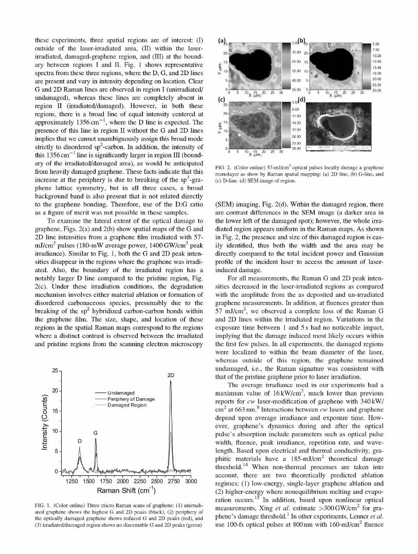
these experiments, three spatial regions are of interest: (I) outside of the laser-irradiated área, (II) within the laser-irradiated, damaged-graphene región, and (III) at the bound-ary between regions I and II. Fig. 1 shows representative spectra from these three regions, where the D, G, and 2D lines are present and vary in intensity depending on location. Clear G and 2D Raman lines are observed in región I (unirradiated/ undamaged), whereas these lines are completely absent in región II (irradiated/damaged). However, in both these regions, there is a broad line of equal intensity centered at approximately 1356 cm~ , where the D line is expected. The presence of this line in región II without the G and 2D lines implies that we cannot unambiguously assign this broad mode strictly to disordered sp -carbón. In addition, the intensity of this 1356cm~ line is significantly larger in región III (bound-ary of the irradiated/damaged área), as would be anticipated from heavily damaged graphene. These facts indicate that this increase at the periphery is due to breaking of the sp -graphene lattice symmetry, but in all three cases, a broad background band is also present that is not related directly to the graphene bonding. Therefore, use of the D:G ratio as a figure of merit was not possible in these samples.
To examine the lateral extent of the optical damage to graphene, Figs. 2(a) and 2(b) show spatial maps of the G and 2D line intensities from a graphene film irradiated with 57-mJ/cm pulses (180-mW average power, 1400 GW/cm peak irradiance). Similar to Fig. 1, both the G and 2D peak intensities disappear in the regions where the graphene was irradiated. Also, the boundary of the irradiated región has a notably larger D line compared to the pristine región, Fig. 2(c). Under these irradiation conditions, the degradation mechanism involves either material ablation or formation of disordered carbonaceous species, presumably due to the breaking of the sp hybridized carbon-carbon bonds within the graphene film. The size, shape, and location of these regions in the spatial Raman maps correspond to the regions where a distinct contrast is observed between the irradiated and pristine regions from the scanning electrón microscopy
c o O
25-,
20-
15-
Tr, 10
5-
2D
-Undamaged - Periphery of Damage Damaged Región
1250 ' 1500 ' 1750 2000 ' 2250 ' 2500 ' 2750 ' 3000
Raman Shift (crrf )
FIG. 1. (Color oniine) Three micro Raman scans of graphene: (1) unirradiated graphene shows the highest G and 2D peaks (black), (2) periphery of the optically damaged graphene shows reduced G and 2D peaks (red), and (3) irradiated/damaged región shows no discernable G and 2D peaks (green)
10, , 1 5 20 25 30
Xftun)
FIG. 2. (Color online) 57-mJ/cm optical pulses locally damage a graphene monolayer as show by Raman spatial mapping: (a) 2D line, (b) G-line, and (c) D-line. (d) SEM image of región.
(SEM) imaging, Fig. 2(d). Within the damaged región, there are contrast differences in the SEM image (a darker área in the lower left of the damaged spot); however, the whole irradiated región appears uniform in the Raman maps. As shown in Fig. 2, the presence and size of this damaged región is eas-ily identified, thus both the width and the área may be directly compared to the total incident power and Gaussian profile of the incident láser to access the amount of laser-induced damage.
For all measurements, the Raman G and 2D peak intensities decreased in the laser-irradiated regions as compared with the amplitude from the as deposited and un-irradiated graphene measurements. In addition, at fluences greater than 57 mJ/cm , we observed a complete loss of the Raman G and 2D lines within the irradiated región. Variations in the exposure time between 1 and 5 s had no noticeable impact, implying that the damage induced most likely occurs within the first few pulses. In all experiments, the damaged regions were localized to within the beam diameter of the láser, whereas outside of this región, the graphene remained undamaged, Le., the Raman signature was consistent with that of the pristine graphene prior to láser irradiation.
The average irradiance used in our experiments had a máximum valué of 16kW/cm , much lower than previous reports for cw laser-modification of graphene with 340 kW/ cm at 663 nm. Interactions between cw lasers and graphene depend upon average irradiance and exposure time. However, graphene's dynamics during and after the optical pulse 's absorption include parameters such as optical pulse width, fluence, peak irradiance, repetition rate, and wave-length. Based upon electrical and thermal conductivity, gra-phitic materials have a 185-mJ/cm theoretical damage threshold. When non-thermal processes are taken into account, there are two theoretically predicted ablation regimes: (1) low-energy, single-layer graphene ablation and (2) higher-energy where nonequilibrium melting and evapo-ration occurs. In addition, based upon nonlinear optical measurements, Xing et al. estímate >300 GW/cm for graphene's damage threshold. In other experiments, Lenner et al. use 100-fs optical pulses at 800 nm with 160-mJ/cm fluence

E
—; ro
<. 0)
m 'r-m U
500
400
300
200
1110
O1 ' ' ' 0' ' ' ' 0 20 40 60 0 20 40 60
Optical Fluence [mJ/cm ] Optical Fluence [mJ/cm ]
FIG. 3. (Color onlrne) SEM image analysis measured the (a) laser-rnduced damage área and (b) major (O) and mrnor (+) axes of an ellipse fit to the damaged área.
to ablate graphite.12 Our results illustrate stractural damage to graphene at a much lower fluence (14—66 mJ/cm2) than that used to ablate graphite, shown in the Raman spatial plots, thus, demonstrating our ability to disrupt the sp2 carbón bonding thereby locally modifying graphene.
Analysis of the SEM images, e.g., Fig. 2(d), was used to quantify the optically induced damage área and is shown in Fig. 3(a) as a function of optical fluence. In general, the optical damage manifested itself as a pear-shaped región which was fit with an ellipse. Fig. 3 plots the damage dependence on the major and minor ellipse axes as a function of fluence. The size of the optical damage increased linearly with optical fluence.
In all cases, the pear-shaped damaged área was smaller than the measured 40-fim diameter of our focused láser. The measured diameter (1/e2 optical power) of the Gaussian spatial profile was monitored along one axis, thus, the peak irra-diance occurs over a diameter smaller than our measured 40-fim diameter, and the ellipticity is likely due to an aberra-tion in the focus rather than a physical damage mechanism of the single-layer graphene. The linear fit to the damaged área suggests that our experiments are far above the damage threshold.
The láser pulse parameters for the onset of damage are important for examining the performance and limitation of graphene-based optic and photonic devices, e.g., a 4-GW/ cm2 optical saturable absorber.1 We performed a quantitative study with femtosecond optical pulses to establish the onset of damage in CVD grown graphene films transferred onto sapphire substrates. Our average irradiances (3-16kW/cm2) were at least an order of magnitude below those used for graphene patterning using cw lasers. We damaged the films with a fluence as low as 14 mJ/cm2. This fluence is far below
those previously found to ablate graphite, and well below theoretical predictions for the damage threshold of graphene, as well as more than two-orders-of-magnitude below the multiphoton ablation threshold (3000 mJ/cm ) of the sapphire substrate. Using micro-Raman spectroscopy, we were able to measure the changes in the G and 2D lines to determine the extent of the damage and were able to measure the área of the damaged región using SEM imaging. The laser-induced damage was localized without disturbing the surrounding graphene regions demonstrating a potential tool for patterning graphene. Further work is needed to under-stand the behavior of the carbón bonds during and following láser irradiation and to determine if this process has utility, for example, in local reordering of the bond structure for local bandgap creation in multi-layer graphene.
LG. Xing, H. Guo, X. Zhang, T. C. Sum, and C. H. A. Huan, Opt. Express 18,4564(2010).
2H. Zhang, Q. Bao, D. Tang, L. Zhao, and K. Loh, Appl. Phys. Lett. 95, 141103(2009).
3H. Yu, X. Chen, H. Zhang, X. Xu, X. Hu, Z. Wang, J. Wang, S. Zhuang, and M. Jiang, ACS Nano 4, 7582 (2010).
4C. Berger, Z. M. Song, T. B. Li, X. B. Li, A. Y. Ogbazghi, R. Feng, Z. T. Dai, A. N. Marchenkov, E. H. Conrad, P. N. First et al, J. Phys. Chem. 108, 19912(2004).
5X. S. Li, W. W. Cai, J. H. An, S. Kim, J. Nah, D. X. Yang, R. Piner, A. Velamakanni, I. Jung, E. Tutuc et al, Science 324, 1312 (2009).
5J. D. Caldwell, T. J. Anderson, J. C. Culbertson, G. G. Jernigan, K. D. Hobart, F. J. Kub, M. J. Tadjer, J. L. Tedesco, J. K. Hite, M. A. Mastro et al, ACS Nano 4, 1108 (2010).
7S. Unarunotai, Y. Murata, C. E. Chialvo, H.-S. Kim, S. MacLaren, N. Masón, I. Petrov, and J. A. Rogers, Appl. Phys. Lett. 95, 202101 (2009).
8Y. Zhou, Q. Bao, B. Varghese, L. A. L. Tang, C. K. Tan, C. Sow, and K. P. Loh, Adv. Mater. 22, 67 (2010).
9Z. Wei, D. Wang, S. Kim, S. Kim, Y. Hu, M. K. Yakes, A. R. Laracuente, Z. Dai, S. R. Marder, C. Berger et al, Science 328, 1373 (2010).
10X. Liu, D. Du, and G Mourou, IEEE J. Quantum Electron. 33, 1706 (1997).
UM. Lenner, A. Kaplan, and R. E. Palmer, Appl. Phys. Lett. 90, 153119 (2007).
I2M. Lenner, A. Kaplan, C. Huchon, and R. E. Palmer, Phys. Rev. B 79, 184105(2009).
13F. Tuinstra and J. Koenig, J. Chem. Phys. 53, 1126 (1970). K. Sokolowski-Tinten, S. Kudryashov, V. Temnov, J. Bialkowski, D. Von der Linde, A. Cavalleri, H. O. Jeschke, M. E. Garcia, and K. H. Benne-mann, Ultrafast Phenomena XII, Sprtnger Series in Chemical Physics Vol. 66, edited by T. Elsaesser, S. Mukamel, M. M. Murnane, and N. F. Scherer (Springer, Berlin, 2001), pp. 425^27.
I5H. O. Jeschke, M. E. Garcia, and K. H. Bennemann, Phys. Rev. Lett. 87, 87 (2001).
16D. Ashkenasi, R. Stoian, and A. Rosenfeld, Appl. Surf. Sci. 154-155, 40 (2000).