Quad, 16-Bit nanoDAC+ with 4 ppm/°C Reference, SPI ...
17
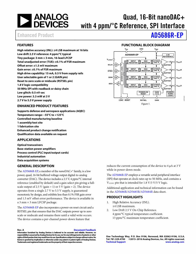
Quad, 16-Bit nanoDAC+ with 4 ppm/°C Reference, SPI Interface Enhanced Product AD5686R-EP Rev. A Document Feedback Information furnished by Analog Devices is believed to be accurate and reliable. However, no responsibility is assumed by Analog Devices for its use, nor for any infringements of patents or other rights of third parties that may result from its use. Specifications subject to change without notice. No license is granted by implication or otherwise under any patent or patent rights of Analog Devices. Trademarks and registered trademarks are the property of their respective owners. One Technology Way, P.O. Box 9106, Norwood, MA 02062-9106, U.S.A. Tel: 781.329.4700 ©2015–2016 Analog Devices, Inc. All rights reserved. Technical Support www.analog.com FEATURES High relative accuracy (INL): ±4 LSB maximum at 16 bits Low drift 2.5 V reference: 4 ppm/°C typical Tiny package: 3 mm × 3 mm, 16-lead LFCSP Total unadjusted error (TUE): ±0.1% of FSR maximum Offset error: ±1.5 mV maximum Gain error: ±0.1% of FSR maximum High drive capability: 15 mA, 0.5 V from supply rails User selectable gain of 1 or 2 (GAIN pin) Reset to zero scale or midscale (RSTSEL pin) 1.8 V logic compatibility 50 MHz SPI with readback or daisy chain Low glitch: 0.5 nV-sec Low power: 3.3 mW at 3 V 2.7 V to 5.5 V power supply ENHANCED PRODUCT FEATURES Supports defense and aerospace applications (AQEC) Temperature range: −55°C to +125°C Controlled manufacturing baseline 1 assembly/test site 1 fabrication site Enhanced product change notification Qualification data available on request APPLICATIONS Optical transceivers Base-station power amplifiers Process control (PLC input/output cards) Industrial automation Data acquisition systems FUNCTIONAL BLOCK DIAGRAM SCLK V LOGIC SYNC SDIN SDO INPUT REGISTER DAC REGISTER STRING DAC A BUFFER V OUT A INPUT REGISTER DAC REGISTER STRING DAC B BUFFER V OUT B INPUT REGISTER DAC REGISTER STRING DAC C BUFFER V OUT C INPUT REGISTER DAC REGISTER STRING DAC D BUFFER V OUT D V REF GND V DD 2.5V REFERENCE POWER- DOWN LOGIC POWER-ON RESET GAIN ×1/×2 INTERFACE LOGIC RSTSEL GAIN LDAC RESET AD5686R-EP 12975-001 Figure 1. GENERAL DESCRIPTION The AD5686R-EP , a member of the nanoDAC+® family, is a low power, quad, 16-bit buffered voltage output digital-to-analog converter (DAC). The device includes a 2.5 V, 4 ppm/°C internal reference (enabled by default) and a gain select pin giving a full- scale output of 2.5 V (gain = 1) or 5 V (gain = 2). The device operates from a single 2.7 V to 5.5 V supply, is guaranteed monotonic by design, and exhibits less than 0.1% FSR gain error and 1.5 mV offset error performance. The device is available in a 3 mm × 3 mm LFCSP package. The AD5686R-EP also incorporates a power-on reset circuit and a RSTSEL pin that ensures that the DAC outputs power up to zero scale or midscale and remains there until a valid write occurs. The device contains a per-channel power-down feature that reduces the current consumption of the device to 4 μA at 3 V while in power-down mode. The AD5686R-EP employs a versatile serial peripheral interface (SPI) that operates at clock rates up to 50 MHz, and contains a VLOGIC pin that is intended for 1.8 V/3 V/5 V logic. Additional application and technical information can be found in the AD5686R/AD5685R/AD5684R data sheet. PRODUCT HIGHLIGHTS 1. High Relative Accuracy (INL). ±4 LSB maximum. 2. Low Drift 2.5 V On-Chip Reference. 4 ppm/°C typical temperature coefficient. 13 ppm/°C maximum temperature coefficient.
Transcript of Quad, 16-Bit nanoDAC+ with 4 ppm/°C Reference, SPI ...
Quad, 16-Bit nanoDAC+ with 4 ppm/°C Reference, SPI Interface
Enhanced Product AD5686R-EP
Rev. A Document Feedback Information furnished by Analog Devices is believed to be accurate and reliable. However, no responsibility is assumed by Analog Devices for its use, nor for any infringements of patents or other rights of third parties that may result from its use. Specifications subject to change without notice. No license is granted by implication or otherwise under any patent or patent rights of Analog Devices. Trademarks and registered trademarks are the property of their respective owners.
One Technology Way, P.O. Box 9106, Norwood, MA 02062-9106, U.S.A.Tel: 781.329.4700 ©2015–2016 Analog Devices, Inc. All rights reserved. Technical Support www.analog.com
FEATURES High relative accuracy (INL): ±4 LSB maximum at 16 bits Low drift 2.5 V reference: 4 ppm/°C typical Tiny package: 3 mm × 3 mm, 16-lead LFCSP Total unadjusted error (TUE): ±0.1% of FSR maximum Offset error: ±1.5 mV maximum Gain error: ±0.1% of FSR maximum High drive capability: 15 mA, 0.5 V from supply rails User selectable gain of 1 or 2 (GAIN pin) Reset to zero scale or midscale (RSTSEL pin) 1.8 V logic compatibility 50 MHz SPI with readback or daisy chain Low glitch: 0.5 nV-sec Low power: 3.3 mW at 3 V 2.7 V to 5.5 V power supply
ENHANCED PRODUCT FEATURES Supports defense and aerospace applications (AQEC) Temperature range: −55°C to +125°C Controlled manufacturing baseline 1 assembly/test site 1 fabrication site Enhanced product change notification Qualification data available on request
APPLICATIONS Optical transceivers Base-station power amplifiers Process control (PLC input/output cards) Industrial automation Data acquisition systems
FUNCTIONAL BLOCK DIAGRAM
SCLK
VLOGIC
SYNC
SDIN
SDO
INPUTREGISTER
DACREGISTER
STRINGDAC A
BUFFER
VOUTA
INPUTREGISTER
DACREGISTER
STRINGDAC B
BUFFER
VOUTB
INPUTREGISTER
DACREGISTER
STRINGDAC C
BUFFER
VOUTC
INPUTREGISTER
DACREGISTER
STRINGDAC D
BUFFER
VOUTD
VREFGNDVDD
2.5VREFERENCE
POWER-DOWNLOGIC
POWER-ONRESET
GAIN×1/×2
INT
ER
FA
CE
LO
GIC
RSTSEL GAINLDAC RESET
AD5686R-EP
12
97
5-0
01
Figure 1.
GENERAL DESCRIPTION The AD5686R-EP, a member of the nanoDAC+® family, is a low power, quad, 16-bit buffered voltage output digital-to-analog converter (DAC). The device includes a 2.5 V, 4 ppm/°C internal reference (enabled by default) and a gain select pin giving a full-scale output of 2.5 V (gain = 1) or 5 V (gain = 2). The device operates from a single 2.7 V to 5.5 V supply, is guaranteed monotonic by design, and exhibits less than 0.1% FSR gain error and 1.5 mV offset error performance. The device is available in a 3 mm × 3 mm LFCSP package.
The AD5686R-EP also incorporates a power-on reset circuit and a RSTSEL pin that ensures that the DAC outputs power up to zero scale or midscale and remains there until a valid write occurs. The device contains a per-channel power-down feature that
reduces the current consumption of the device to 4 μA at 3 V while in power-down mode.
The AD5686R-EP employs a versatile serial peripheral interface (SPI) that operates at clock rates up to 50 MHz, and contains a VLOGIC pin that is intended for 1.8 V/3 V/5 V logic.
Additional application and technical information can be found in the AD5686R/AD5685R/AD5684R data sheet.
PRODUCT HIGHLIGHTS 1. High Relative Accuracy (INL).
±4 LSB maximum. 2. Low Drift 2.5 V On-Chip Reference.
4 ppm/°C typical temperature coefficient. 13 ppm/°C maximum temperature coefficient.

AD5686R-EP Enhanced Product
Rev. A | Page 2 of 17
TABLE OF CONTENTS Features .............................................................................................. 1 Enhanced Product Features ............................................................ 1 Applications ....................................................................................... 1 Functional Block Diagram .............................................................. 1 General Description ......................................................................... 1
Product Highlights ....................................................................... 1 Revision History ........................................................................... 2
Specifications ..................................................................................... 3 AC Characteristics ........................................................................ 5
Timing Characteristics .................................................................6 Daisy-Chain and Readback Timing Characteristics ................7
Absolute Maximum Ratings ............................................................9 ESD Caution...................................................................................9
Pin Configuration and Function Descriptions ........................... 10 Typical Performance Characteristics ........................................... 11 Outline Dimensions ....................................................................... 17
Ordering Guide .......................................................................... 17
REVISION HISTORY 11/2016—Rev. 0 to Rev. A Changed 1.8 V ≤ VLOGIC ≤ 5.5 V to 1.62 V ≤ VLOGIC ≤ 5.5 V ................................................. Throughout Changes to Features Section............................................................ 1 Changes to VLOGIC Parameter, Table 1 ...................................................... 4 Changes to Output Noise Spectral Density (NSD) Parameter, Test Conditions/Comments Column, Table 2 .............................. 5 Changes to Table 3 ............................................................................ 6 Changes to Table 4 and Figure 4 ..................................................... 7 Changes to Figure 5 .......................................................................... 8 Deleted ESD Parameter, Table 5 and FICDM Parameter, Table 5 .... 9 Changes to Pin 9 Description Column, Table 6 and Pin 13 Description Column, Table 6 ........................................................ 10 Changes to Figure 9 ........................................................................ 11 Changes to Figure 15 to Figure 18 ................................................ 12 Changes to Figure 19 to Figure 23 ................................................ 13 Changes to Figure 25, Figure 26, and Figure 29 ......................... 14 Changes to Figure 31 and Figure 36 ............................................. 16 Changes to Figure 37 ...................................................................... 16 7/2015—Revision 0: Initial Version
Enhanced Product AD5686R-EP
Rev. A | Page 3 of 17
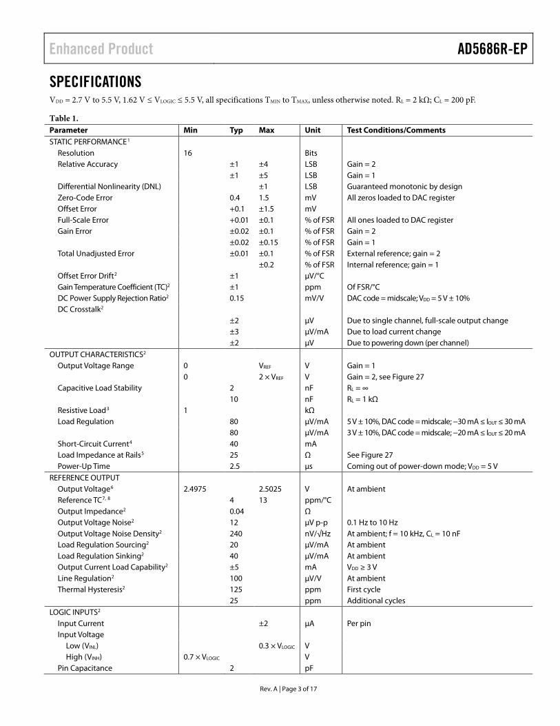
SPECIFICATIONS VDD = 2.7 V to 5.5 V, 1.62 V ≤ VLOGIC ≤ 5.5 V, all specifications TMIN to TMAX, unless otherwise noted. RL = 2 kΩ; CL = 200 pF.
Table 1. Parameter Min Typ Max Unit Test Conditions/Comments STATIC PERFORMANCE1
Resolution 16 Bits Relative Accuracy ±1 ±4 LSB Gain = 2 ±1 ±5 LSB Gain = 1 Differential Nonlinearity (DNL) ±1 LSB Guaranteed monotonic by design Zero-Code Error 0.4 1.5 mV All zeros loaded to DAC register Offset Error +0.1 ±1.5 mV Full-Scale Error +0.01 ±0.1 % of FSR All ones loaded to DAC register Gain Error ±0.02 ±0.1 % of FSR Gain = 2 ±0.02 ±0.15 % of FSR Gain = 1 Total Unadjusted Error ±0.01 ±0.1 % of FSR External reference; gain = 2 ±0.2 % of FSR Internal reference; gain = 1 Offset Error Drift2 ±1 µV/°C Gain Temperature Coefficient (TC)2 ±1 ppm Of FSR/°C DC Power Supply Rejection Ratio2 0.15 mV/V DAC code = midscale; VDD = 5 V ± 10% DC Crosstalk2
±2 µV Due to single channel, full-scale output change ±3 µV/mA Due to load current change ±2 µV Due to powering down (per channel)
OUTPUT CHARACTERISTICS2 Output Voltage Range 0 VREF V Gain = 1 0 2 × VREF V Gain = 2, see Figure 27 Capacitive Load Stability 2 nF RL = ∞ 10 nF RL = 1 kΩ Resistive Load3 1 kΩ Load Regulation 80 µV/mA 5 V ± 10%, DAC code = midscale; −30 mA ≤ IOUT ≤ 30 mA 80 µV/mA 3 V ± 10%, DAC code = midscale; −20 mA ≤ IOUT ≤ 20 mA Short-Circuit Current4 40 mA Load Impedance at Rails5 25 Ω See Figure 27 Power-Up Time 2.5 µs Coming out of power-down mode; VDD = 5 V
REFERENCE OUTPUT Output Voltage6 2.4975 2.5025 V At ambient Reference TC7, 8 4 13 ppm/°C Output Impedance2 0.04 Ω Output Voltage Noise2 12 µV p-p 0.1 Hz to 10 Hz Output Voltage Noise Density2 240 nV/√Hz At ambient; f = 10 kHz, CL = 10 nF Load Regulation Sourcing2 20 µV/mA At ambient Load Regulation Sinking2 40 µV/mA At ambient Output Current Load Capability2 ±5 mA VDD ≥ 3 V
Line Regulation2 100 µV/V At ambient Thermal Hysteresis2 125 ppm First cycle 25 ppm Additional cycles
LOGIC INPUTS2 Input Current ±2 µA Per pin Input Voltage
Low (VINL) 0.3 × VLOGIC V High (VINH) 0.7 × VLOGIC V
Pin Capacitance 2 pF
AD5686R-EP Enhanced Product
Rev. A | Page 4 of 17
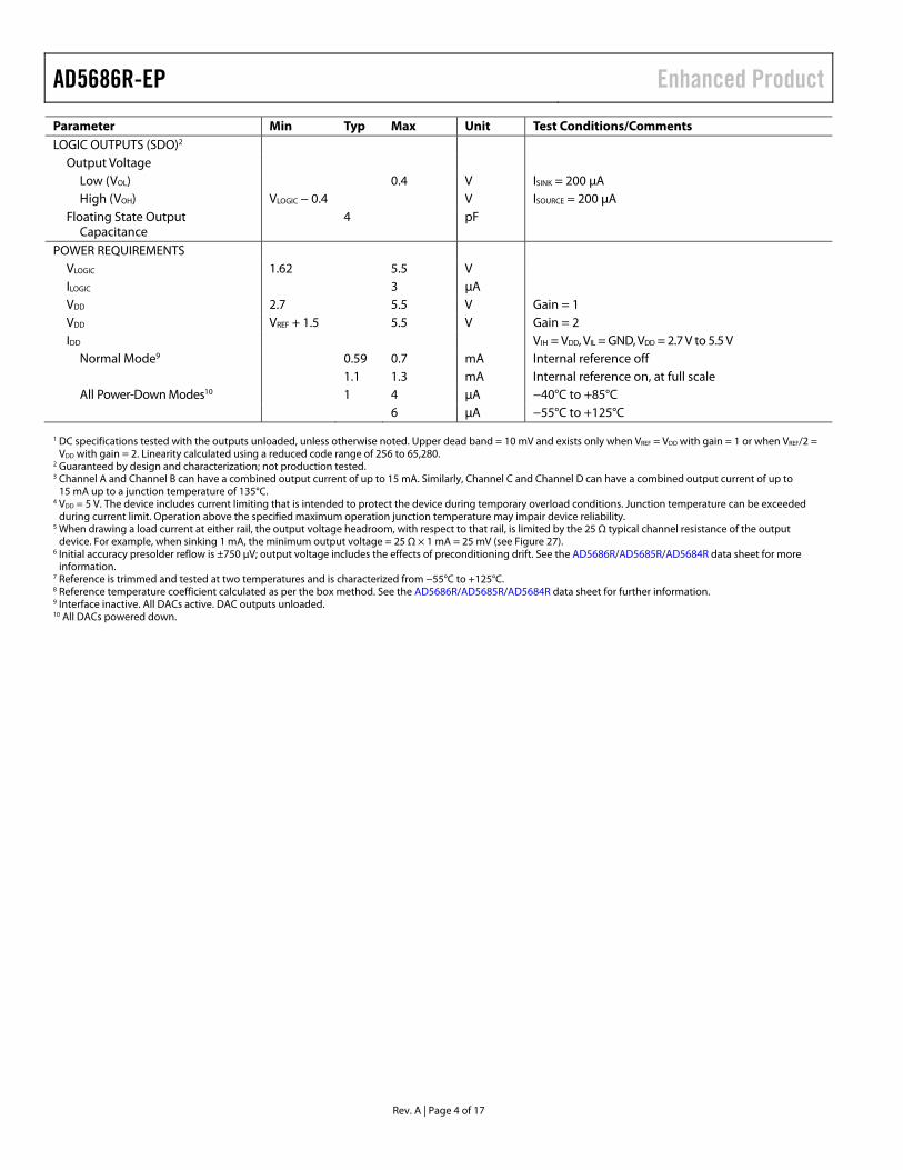
Parameter Min Typ Max Unit Test Conditions/Comments LOGIC OUTPUTS (SDO)2
Output Voltage Low (VOL) 0.4 V ISINK = 200 μA High (VOH) VLOGIC − 0.4 V ISOURCE = 200 μA
Floating State Output Capacitance
4 pF
POWER REQUIREMENTS VLOGIC 1.62 5.5 V ILOGIC 3 μA VDD 2.7 5.5 V Gain = 1 VDD VREF + 1.5 5.5 V Gain = 2 IDD VIH = VDD, VIL = GND, VDD = 2.7 V to 5.5 V
Normal Mode9 0.59 0.7 mA Internal reference off 1.1 1.3 mA Internal reference on, at full scale All Power-Down Modes10 1 4 μA −40°C to +85°C
6 μA −55°C to +125°C 1 DC specifications tested with the outputs unloaded, unless otherwise noted. Upper dead band = 10 mV and exists only when VREF = VDD with gain = 1 or when VREF/2 =
VDD with gain = 2. Linearity calculated using a reduced code range of 256 to 65,280. 2 Guaranteed by design and characterization; not production tested. 3 Channel A and Channel B can have a combined output current of up to 15 mA. Similarly, Channel C and Channel D can have a combined output current of up to
15 mA up to a junction temperature of 135°C. 4 VDD = 5 V. The device includes current limiting that is intended to protect the device during temporary overload conditions. Junction temperature can be exceeded
during current limit. Operation above the specified maximum operation junction temperature may impair device reliability. 5 When drawing a load current at either rail, the output voltage headroom, with respect to that rail, is limited by the 25 Ω typical channel resistance of the output
device. For example, when sinking 1 mA, the minimum output voltage = 25 Ω × 1 mA = 25 mV (see Figure 27). 6 Initial accuracy presolder reflow is ±750 μV; output voltage includes the effects of preconditioning drift. See the AD5686R/AD5685R/AD5684R data sheet for more
information. 7 Reference is trimmed and tested at two temperatures and is characterized from −55°C to +125°C. 8 Reference temperature coefficient calculated as per the box method. See the AD5686R/AD5685R/AD5684R data sheet for further information. 9 Interface inactive. All DACs active. DAC outputs unloaded. 10 All DACs powered down.

Enhanced Product AD5686R-EP
Rev. A | Page 5 of 17
AC CHARACTERISTICS VDD = 2.7 V to 5.5 V, RL = 2 kΩ to GND, CL = 200 pF to GND, 1.62 V ≤ VLOGIC ≤ 5.5 V, and all specifications TMIN to TMAX, unless otherwise noted. Guaranteed by design and characterization, not production tested.
Table 2. Parameter1 Min Typ Max Unit Test Conditions/Comments2 Output Voltage Settling Time 5 8 μs ¼ to ¾ scale settling to ±2 LSB Slew Rate 0.8 V/μs Digital-to-Analog Glitch Impulse 0.5 nV-sec 1 LSB change around major carry Digital Feedthrough 0.13 nV-sec Digital Crosstalk 0.1 nV-sec Analog Crosstalk 0.2 nV-sec DAC-to-DAC Crosstalk 0.3 nV-sec Total Harmonic Distortion (THD)3 −80 dB At ambient, bandwidth (BW) = 20 kHz, VDD = 5 V, fOUT = 1 kHz Output Noise Spectral Density (NSD) 300 nV/√Hz DAC code = midscale, 10 kHz; gain = 2, internal reference Output Noise 6 μV p-p 0.1 Hz to 10 Hz Signal-to-Noise Ratio (SNR) 90 dB At ambient, BW = 20 kHz, VDD = 5 V, fOUT = 1 kHz Spurious Free Dynamic Range (SFDR) 83 dB At ambient, BW = 20 kHz, VDD = 5 V, fOUT = 1 kHz Signal-to-Noise-and-Distortion Ratio (SINAD) 80 dB At ambient, BW = 20 kHz, VDD = 5 V, fOUT = 1 kHz 1 See the AD5686R/AD5685R/AD5684R data sheet. 2 Temperature range is −55°C to +125°C, typical at 25°C. 3 Digitally generated sine wave at 1 kHz.
AD5686R-EP Enhanced Product
Rev. A | Page 6 of 17
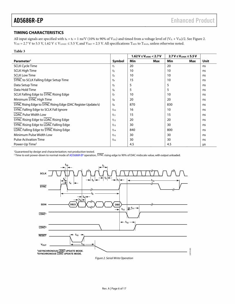
TIMING CHARACTERISTICS All input signals are specified with tR = tF = 1 ns/V (10% to 90% of VDD) and timed from a voltage level of (VIL + VIH)/2. See Figure 2. VDD = 2.7 V to 5.5 V, 1.62 V ≤ VLOGIC ≤ 5.5 V, and VREF = 2.5 V. All specifications TMIN to TMAX, unless otherwise noted.
Table 3 1.62 V ≤ VLOGIC < 2.7 V 2.7 V ≤ VLOGIC ≤ 5.5 V Parameter1 Symbol Min Max Min Max Unit SCLK Cycle Time t1 20 20 ns SCLK High Time t2 10 10 ns SCLK Low Time t3 10 10 ns SYNCE to SCLK Falling Edge Setup Time t4 15 10 ns
Data Setup Time t5 5 5 ns Data Hold Time t6 5 5 ns SCLK Falling Edge to SYNCE Rising Edge t7 10 10 ns
Minimum SYNCE High Time t8 20 20 ns
SYNCE Rising Edge to SYNCE Rising Edge (DAC Register Update/s) t9 870 830 ns
SYNCE Falling Edge to SCLK Fall Ignore t10 16 10 ns
LDACE Pulse Width Low t11 15 15 ns
SYNCE Rising Edge to LDACE Rising Edge t12 20 20 ns
SYNCE Rising Edge to LDACE Falling Edge t13 30 30 ns
LDACE Falling Edge to SYNCE Rising Edge t14 840 800 ns
Minimum Pulse Width Low t15 30 30 ns Pulse Activation Time t16 30 30 ns Power-Up Time2 4.5 4.5 μs 1Guaranteed by design and characterization; not production tested. 2 Time to exit power-down to normal mode of AD5686R-EP operation, SYNCE rising edge to 90% of DAC midscale value, with output unloaded.
t4
t3
SCLK
SYNC
SDIN
t1
t2
t5
t6
t7t8
DB23
t10
t11
t12
LDAC1
LDAC2
t13
1ASYNCHRONOUS LDAC UPDATE MODE.2SYNCHRONOUS LDAC UPDATE MODE.
RESET t15
t16VOUT
DB0
129
75-0
02
t14
t9
Figure 2. Serial Write Operation

Enhanced Product AD5686R-EP
Rev. A | Page 7 of 17
DAISY-CHAIN AND READBACK TIMING CHARACTERISTICS All input signals are specified with tR = tF = 1 ns/V (10% to 90% of VDD) and timed from a voltage level of (VIL + VIH)/2. See Figure 4 and Figure 5. VDD = 2.7 V to 5.5 V, 1.62 V ≤ VLOGIC ≤ 5.5 V, and VREF = 2.5 V. All specifications TMIN to TMAX, unless otherwise noted.
Table 4. 1.62 V ≤ VLOGIC < 2.7 V 2.7 V ≤ VLOGIC ≤ 5.5 V Parameter1 Symbol Min Max Min Max Unit SCLK Cycle Time t1 66 40 ns SCLK High Time t2 33 20 ns SCLK Low Time t3 33 20 ns SYNCE to SCLK Falling Edge t4 33 20 ns
Data Setup Time t5 5 5 ns Data Hold Time t6 5 5 ns SCLK Falling Edge to SYNCE Rising Edge t7 15 10 ns
Minimum SYNCE High Time t8 60 30 ns
SDO Data Valid from SCLK Rising Edge t9 45 30 ns SYNCE Rising Edge to SCLK Rising Edge t10 15 10 ns
SYNCE Rising Edge to SDO Disable t11 60 60 ns 1 Guaranteed by design and characterization; not production tested.
Circuit and Timing Diagrams
200µA IOL
200µA IOH
VOH (MIN)TO OUTPUTPIN
CL20pF
1297
5-0
03
Figure 3. Load Circuit for Digital Output (SDO) Timing Specifications
t4
t5
t6
t8
t1
t2
t3
SDO
SDIN
SYNC
SCLK 4824
DB23 DB0 DB23 DB0
DB23
INPUT WORD FOR DAC NUNDEFINED
INPUT WORD FOR DAC N + 1INPUT WORD FOR DAC N
DB0
t7
t10
t9
12
975
-004
Figure 4. Daisy-Chain Timing Diagram

AD5686R-EP Enhanced Product
Rev. A | Page 8 of 17
SYNC
t8
t6
SCLK 241 241
t8t4 t2t7
t3
t1
DB23 DB0 DB23 DB0
t10
SDIN
NOP CONDITIONINPUT WORD SPECIFIESREGISTER TO BE READ
t5
DB23 DB0SDO
SELECTED REGISTER DATACLOCKED OUT
HI-Z
t9 t11
129
75-
005
Figure 5. Readback Timing Diagram

Enhanced Product AD5686R-EP
Rev. A | Page 9 of 17
ABSOLUTE MAXIMUM RATINGS TA = 25°C, unless otherwise noted.
Table 5. Parameter Rating VDD to GND −0.3 V to +7 V VLOGIC to GND −0.3 V to +7 V VOUT to GND −0.3 V to VDD + 0.3 V VREF to GND −0.3 V to VDD + 0.3 V Digital Input Voltage to GND −0.3 V to VLOGIC + 0.3 V Operating Temperature Range −55°C to +125°C Storage Temperature Range −65°C to +150°C Junction Temperature 135°C 16-Lead LFCSP, θJA Thermal Impedance,
θJA Airflow (4-Layer Board) 70°C/W
Reflow Soldering Peak Temperature, Pb Free (J-STD-020)
260°C
Stresses at or above those listed under Absolute Maximum Ratings may cause permanent damage to the product. This is a stress rating only; functional operation of the product at these or any other conditions above those indicated in the operational section of this specification is not implied. Operation beyond the maximum operating conditions for extended periods may affect product reliability.
ESD CAUTION

AD5686R-EP Enhanced Product
Rev. A | Page 10 of 17
PIN CONFIGURATION AND FUNCTION DESCRIPTIONS
12
11
10
1
3
4
SDIN
SYNC
SCLK
9 VLOGIC
VOUTA
VDD
2GND
VOUTC
6S
DO
5V
OU
TD
7L
DA
C
8G
AIN
16V
OU
TB
15V
RE
F
14R
ST
SE
L
13R
ES
ET
NOTES1. THE EXPOSED PAD MUST BE TIED TO GND.
TOP VIEW(Not to Scale)
129
75
-00
6
AD5686R-EP
Figure 6. 16-Lead LFCSP Pin Configuration
Table 6. Pin Function Descriptions Pin No. Mnemonic Description 1 VOUTA Analog Output Voltage from DAC A. The output amplifier has rail-to-rail operation. 2 GND Ground Reference Point for All Circuitry on the Device. 3 VDD Power Supply Input. The AD5686R-EP can be operated from 2.7 V to 5.5 V, and the supply must be decoupled
with a 10 μF capacitor in parallel with a 0.1 μF capacitor to GND. 4 VOUTC Analog Output Voltage from DAC C. The output amplifier has rail-to-rail operation. 5 VOUTD Analog Output Voltage from DAC D. The output amplifier has rail-to-rail operation. 6 SDO Serial Data Output. SDO can be used to daisy-chain a number of AD5686R-EP devices together, or it can be used
for readback. The serial data is transferred on the rising edge of SCLK and is valid on the falling edge of the clock. 7 LDACE LDACE can be operated in two modes, asynchronously and synchronously. Pulsing this pin low allows any or all
DAC registers to be updated if the input registers have new data. This allows all DAC outputs to update simultaneously. This pin can also be tied permanently low.
8 GAIN Span Set Pin. When this pin is tied to GND, all four DAC outputs have a span from 0 V to VREF. If this pin is tied to VLOGIC, all four DACs output a span of 0 V to 2 × VREF.
9 VLOGIC Digital Power Supply. Voltage ranges from 1.62 V to 5.5 V. 10 SCLK Serial Clock Input. Data is clocked into the input shift register on the falling edge of the serial clock input. Data
can be transferred at rates of up to 50 MHz. 11 SYNC E Active Low Control Input. This is the frame synchronization signal for the input data. When SYNCE goes low,
data is transferred in on the falling edges of the next 24 clocks. 12 SDIN Serial Data Input. This device has a 24-bit input shift register. Data is clocked into the register on the falling
edge of the serial clock input. 13 RESETE Asynchronous Reset Input. The RESETE input is falling edge sensitive. When RESETE is low, all LDACE pulses are
ignored. When RESETE is activated, the input register and the DAC register are updated with zero scale or midscale, depending on the state of the RSTSEL pin. If this pin is forced low at power-up, the power-on reset (POR) circuit will not initialize the device correctly until this pin is released.
14 RSTSEL Power-On Reset Pin. Tying this pin to GND powers up all four DACs to zero scale. Tying this pin to VLOGIC powers up all four DACs to midscale.
15 VREF Reference Voltage. The AD5686R-EP has a common reference pin. When using the internal reference, this is the reference output pin. When using an external reference, this is the reference input pin. The default for this pin is as a reference output.
16 VOUTB Analog Output Voltage from DAC B. The output amplifier has rail-to-rail operation. 17 EPAD Exposed Pad. The exposed pad must be tied to GND.
Enhanced Product AD5686R-EP
Rev. A | Page 11 of 17
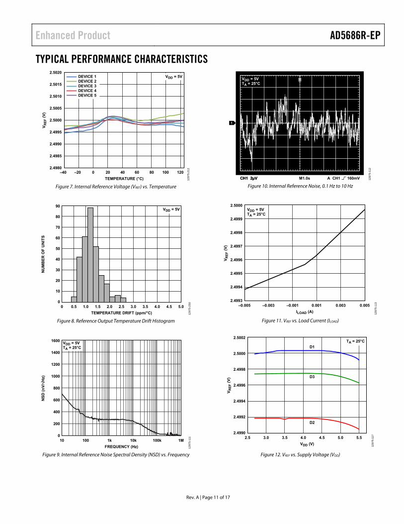
TYPICAL PERFORMANCE CHARACTERISTICS
–40 –20 0 20 40 60 80 100 120
VR
EF (
V)
TEMPERATURE (°C)
DEVICE 1DEVICE 2DEVICE 3DEVICE 4DEVICE 5
2.4980
2.4985
2.4990
2.4995
2.5000
2.5005
2.5010
2.5015
2.5020VDD = 5V
12
975
-21
2Figure 7. Internal Reference Voltage (VREF) vs. Temperature
90
0
10
20
30
40
50
60
70
80
0 0.5 1.0 1.5 2.0 2.5 3.0 3.5 4.0 4.5 5.0
NU
MB
ER
OF
UN
ITS
TEMPERATURE DRIFT (ppm/°C)
VDD = 5V
129
75
-25
0
Figure 8. Reference Output Temperature Drift Histogram
1600
0
200
400
600
800
1000
1200
1400
10 100 1k 10k 100k 1M
NS
D (
nV
/ H
z)
FREQUENCY (Hz)
VDD = 5VTA = 25°C
12
975
-111
Figure 9. Internal Reference Noise Spectral Density (NSD) vs. Frequency
CH1 2µVCH1 2µV M1.0s A CH1 160mV
1
TVDD = 5VTA = 25°C
129
75-
112
Figure 10. Internal Reference Noise, 0.1 Hz to 10 Hz
2.5000
2.4999
2.4998
2.4997
2.4996
2.4995
2.4994
2.4993–0.005 –0.003 –0.001 0.001 0.003 0.005
VR
EF (
V)
ILOAD (A)
VDD = 5VTA = 25°C
129
75-1
13
Figure 11. VREF vs. Load Current (ILOAD)
2.5002
2.5000
2.4998
2.4996
2.4994
2.4992
2.49902.5 3.0 3.5 4.0 4.5 5.0 5.5
VR
EF (
V)
VDD (V)
D1
D3
D2
TA = 25°C
129
75-1
17
Figure 12. VREF vs. Supply Voltage (VDD)

AD5686R-EP Enhanced Product
Rev. A | Page 12 of 17
10
–10
–8
–6
–4
–2
0
2
4
8
6
0 10000 20000 30000 40000 50000 60000
INL
(L
SB
)
CODE
VDD = 5VTA = 25°CINTERNAL REFERENCE = 2.5V
12
975
-11
8
Figure 13. Integral Nonlinearity (INL) vs. Code
1.0
–1.0
–0.8
–0.6
–0.4
–0.2
0
0.2
0.4
0.8
0.6
0 10000 20000 30000 40000 50000 60000
DN
L (
LS
B)
CODE
VDD = 5VTA = 25°CINTERNAL REFERENCE = 2.5V
12
975
-12
1
Figure 14. Differential Nonlinearity (DNL) vs. Code
10
–10
–8
–6
–4
–2
0
2
4
6
8
–40 1106010
ER
RO
R (
LS
B)
TEMPERATURE (°C)
INL
DNL
VDD = 5VINTERNAL REFERENCE = 2.5V
12
975
-12
4
Figure 15. INL Error and DNL Error vs. Temperature
10
–10
–8
–6
–4
–2
0
2
4
6
8
0 5.04.54.03.53.02.52.01.51.00.5
ER
RO
R (
LS
B)
VREF (V)
INL
DNL
VDD = 5VTA = 25°C
129
75-1
25
Figure 16. INL Error and DNL Error vs. VREF
10
–10
–8
–6
–4
–2
0
2
4
6
8
2.7 5.24.74.23.73.2
ER
RO
R (
LS
B)
SUPPLY VOLTAGE (V)
INL
DNL
TA = 25°CINTERNAL REFERENCE = 2.5V
12
975
-12
6
Figure 17. INL Error and DNL Error vs. Supply Voltage
0.10
–0.10
–0.08
–0.06
–0.04
–0.02
0
0.02
0.04
0.06
0.08
–40 –20 0 20 40 60 80 100 120
ER
RO
R (
% o
f F
SR
)
TEMPERATURE (°C)
GAIN ERROR
FULL-SCALE ERROR
VDD = 5VINTERNAL REFERENCE = 2.5V
12
975
-12
7
Figure 18. Gain Error and Full-Scale Error vs. Temperature
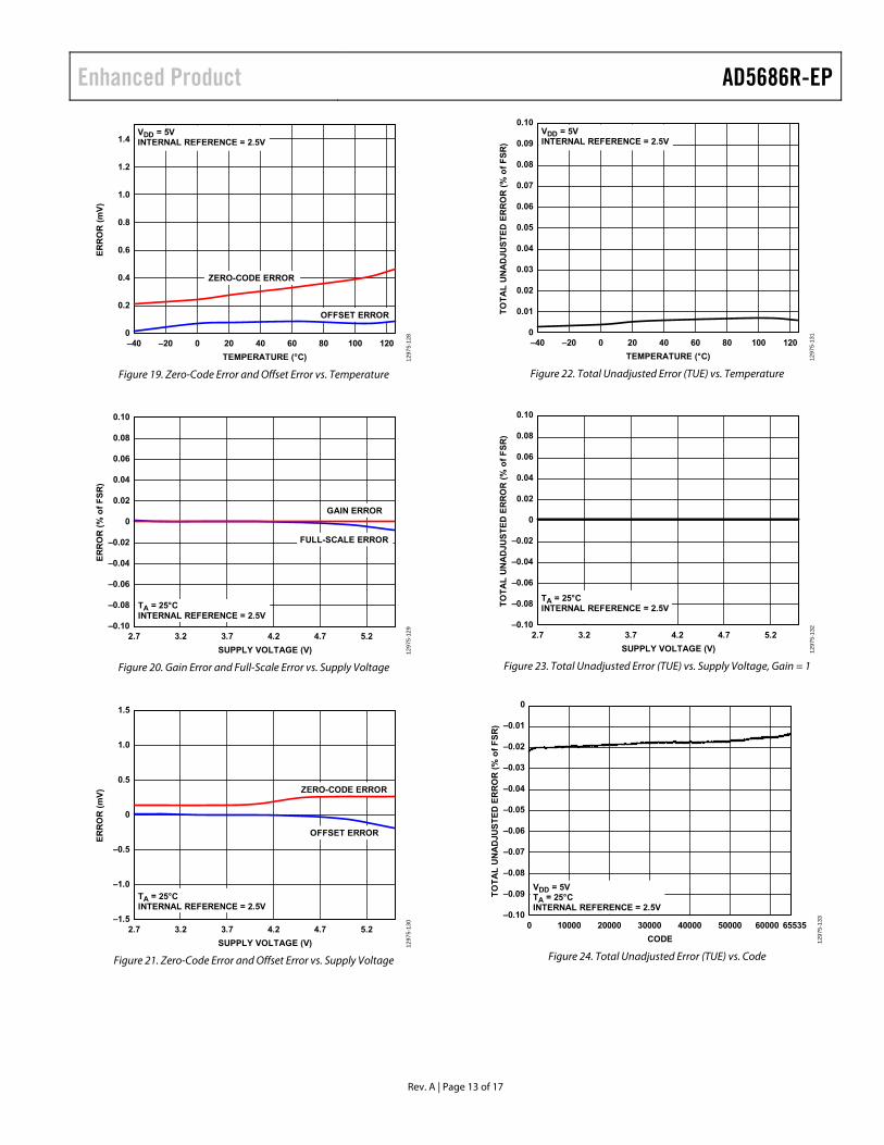
Enhanced Product AD5686R-EP
Rev. A | Page 13 of 17
1.4
1.2
1.0
0.8
0.6
0.4
0.2
0–40 –20 0 20 40 60 80 100 120
ER
RO
R (
mV
)
TEMPERATURE (°C)
OFFSET ERROR
ZERO-CODE ERROR
VDD = 5VINTERNAL REFERENCE = 2.5V
129
75-
128
Figure 19. Zero-Code Error and Offset Error vs. Temperature
0.10
–0.10
–0.08
–0.06
–0.04
–0.02
0
0.02
0.04
0.06
0.08
2.7 5.24.74.23.73.2
ER
RO
R (
% o
f F
SR
)
SUPPLY VOLTAGE (V)
GAIN ERROR
FULL-SCALE ERROR
TA = 25°CINTERNAL REFERENCE = 2.5V
12
975
-12
9
Figure 20. Gain Error and Full-Scale Error vs. Supply Voltage
1.5
–1.5
–1.0
–0.5
0
0.5
1.0
2.7 5.24.74.23.73.2
ER
RO
R (
mV
)
SUPPLY VOLTAGE (V)
ZERO-CODE ERROR
OFFSET ERROR
TA = 25°CINTERNAL REFERENCE = 2.5V
12
975
-13
0
Figure 21. Zero-Code Error and Offset Error vs. Supply Voltage
0.10
0.09
0.08
0.07
0.06
0.05
0.04
0.03
0.02
0.01
0–40 –20 0 20 40 60 80 100 120
TO
TA
L U
NA
DJU
ST
ED
ER
RO
R (
% o
f F
SR
)
TEMPERATURE (°C)
VDD = 5VINTERNAL REFERENCE = 2.5V
12
975-
13
1
Figure 22. Total Unadjusted Error (TUE) vs. Temperature
0.10
0.08
0.06
0.04
0.02
0
–0.02
–0.04
–0.06
–0.08
–0.102.7 5.24.74.23.73.2
TO
TA
L U
NA
DJU
ST
ED
ER
RO
R (
% o
f F
SR
)
SUPPLY VOLTAGE (V)
TA = 25°CINTERNAL REFERENCE = 2.5V
12
975-
13
2
Figure 23. Total Unadjusted Error (TUE) vs. Supply Voltage, Gain = 1
0
–0.01
–0.02
–0.03
–0.04
–0.05
–0.06
–0.07
–0.08
–0.09
–0.100 10000 20000 30000 40000 50000 60000 65535
TO
TA
L U
NA
DJU
ST
ED
ER
RO
R (
% o
f F
SR
)
CODE
VDD = 5VTA = 25°CINTERNAL REFERENCE = 2.5V
12
975
-133
Figure 24. Total Unadjusted Error (TUE) vs. Code

AD5686R-EP Enhanced Product
Rev. A | Page 14 of 17
25
20
15
10
5
0540 560 580 600 620 640
HIT
S
IDD (µA)
VDD = 5VTA = 25°CEXTERNALREFERENCE = 2.5V
129
75-1
35
Figure 25. IDD Histogram with External Reference, 5 V
30
25
20
15
10
5
01000 1020 1040 1060 1080 1100 1120 1140
HIT
S
IDD (µA)
VDD = 5VTA = 25°CINTERNALREFERENCE = 2.5V
129
75-1
36
Figure 26. IDD Histogram with Internal Reference, VREFOUT = 2.5 V, Gain = 2
1.0
–1.0
–0.8
–0.6
–0.4
–0.2
0
0.2
0.4
0.6
0.8
0 5 10 15 20 25 30
∆V
OU
T (
V)
LOAD CURRENT (mA)
SOURCING 2.7V
SOURCING 5V
SINKING 2.7V
SINKING 5V
12
975
-200
Figure 27. Headroom/Footroom vs. Load Current
7
–2
–1
0
1
2
3
4
5
6
–0.06 –0.04 –0.02 0 0.02 0.04 0.06
VO
UT (
V)
LOAD CURRENT (A)
0xFFFF
0x4000
0x8000
0xC000
0x0000
VDD = 5VTA = 25°CGAIN = 2INTERNALREFERENCE = 2.5V
12
975
-138
Figure 28. Source and Sink Capability at 5 V
IOUT (mA) 129
75-
13
9
VO
UT (
V)
–2
–1
0
1
2
3
4
5
–60 –40 –20 0 20 40 60
0xFFFF
0x4000
0x8000
0xC000
0x0000
VDD = 3VTA = 25°CGAIN = 1EXTERNALREFERENCE = 2.5V
Figure 29. Source and Sink Capability at 3 V
0
0.2
0.4
0.6
0.8
1.0
1.2
1.4
–40 1106010
CU
RR
EN
T (
mA
)
TEMPERATURE (°C)
FULL SCALE
ZERO CODE
EXTERNAL REFERENCE, FULL-SCALE
12
975
-14
0
Figure 30. Supply Current vs. Temperature
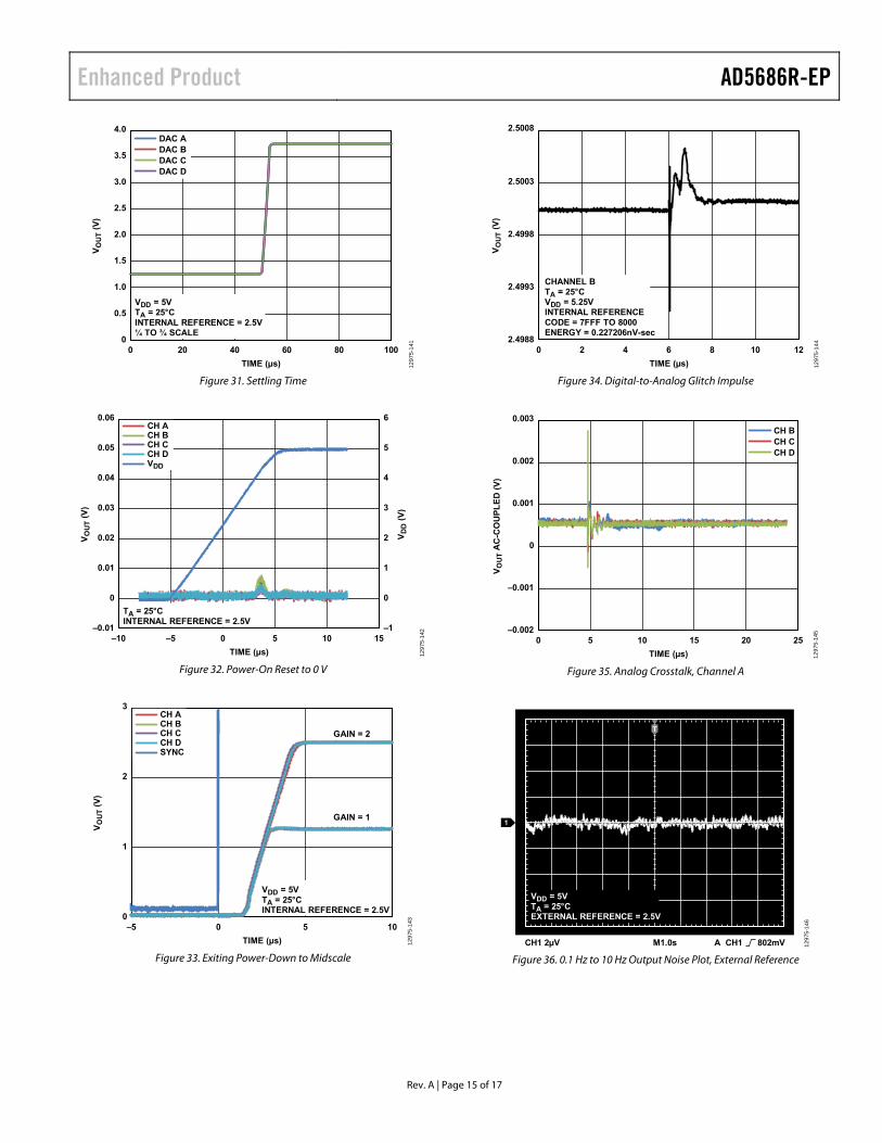
Enhanced Product AD5686R-EP
Rev. A | Page 15 of 17
0
4.0
3.5
3.0
2.5
2.0
1.5
1.0
0.5
0 1008040 6020
VO
UT (
V)
TIME (µs)
DAC ADAC BDAC CDAC D
VDD = 5VTA = 25°CINTERNAL REFERENCE = 2.5V¼ TO ¾ SCALE
12
975
-141
Figure 31. Settling Time
–0.01
0
0.06
0.01
0.02
0.03
0.04
0.05
–1
0
6
1
2
3
4
5
–10 15100 5–5
VO
UT (
V)
VD
D (
V)
TIME (µs)
CH DVDD
CH ACH BCH C
TA = 25°CINTERNAL REFERENCE = 2.5V
12
975
-142
Figure 32. Power-On Reset to 0 V
0
1
3
2
–5 100 5
VO
UT (
V)
TIME (µs)
CH DSYNC
CH ACH BCH C
VDD = 5VTA = 25°CINTERNAL REFERENCE = 2.5V
GAIN = 1
GAIN = 2
12
975
-143
Figure 33. Exiting Power-Down to Midscale
2.4988
2.5008
2.5003
2.4998
2.4993
0 128 104 62
VO
UT (
V)
TIME (µs)
CHANNEL BTA = 25°CVDD = 5.25VINTERNAL REFERENCECODE = 7FFF TO 8000ENERGY = 0.227206nV-sec
12
975
-14
4
Figure 34. Digital-to-Analog Glitch Impulse
–0.002
–0.001
0
0.001
0.002
0.003
0 252010 155
VO
UT A
C-C
OU
PL
ED
(V
)
TIME (µs)
CH BCH CCH D
12
975
-14
5
Figure 35. Analog Crosstalk, Channel A
CH1 2µV M1.0s A CH1 802mV
1
T
VDD = 5VTA = 25°CEXTERNAL REFERENCE = 2.5V
129
75-1
46
Figure 36. 0.1 Hz to 10 Hz Output Noise Plot, External Reference
AD5686R-EP Enhanced Product
Rev. A | Page 16 of 17
CH1 2µV M1.0s A CH1 802mV
1
T
VDD = 5VTA = 25°CINTERNAL REFERENCE = 2.5V
129
75
-14
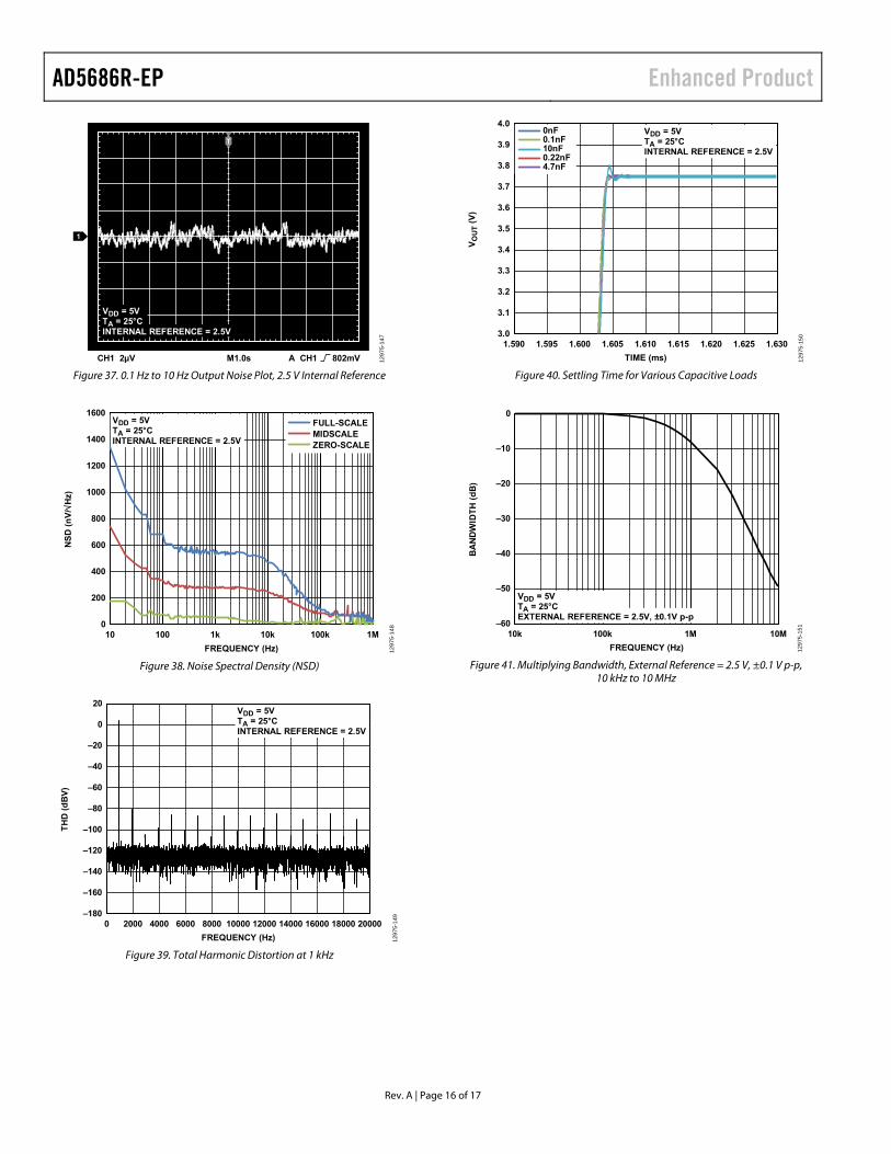
7Figure 37. 0.1 Hz to 10 Hz Output Noise Plot, 2.5 V Internal Reference
0
200
400
600
800
1000
1200
1400
1600
10 1M100k1k 10k100
NS
D (
nV
/ H
z)
FREQUENCY (Hz)
FULL-SCALEMIDSCALEZERO-SCALE
VDD = 5VTA = 25°CINTERNAL REFERENCE = 2.5V
12
97
5-1
48
Figure 38. Noise Spectral Density (NSD)
–180
–160
–140
–120
–100
–80
–60
–40
–20
0
20
0 20000160008000 1200040002000 1800010000 140006000
TH
D (
dB
V)
FREQUENCY (Hz)
VDD = 5VTA = 25°CINTERNAL REFERENCE = 2.5V
129
75-1
49
Figure 39. Total Harmonic Distortion at 1 kHz
3.0
3.1
3.2
3.3
3.4
3.5
3.6
3.7
3.8
3.9
4.0
1.590 1.6301.6201.600 1.610 1.6251.605 1.6151.595
VO
UT (
V)
TIME (ms)
0nF0.1nF10nF0.22nF4.7nF
VDD = 5VTA = 25°CINTERNAL REFERENCE = 2.5V
129
75-1
50
Figure 40. Settling Time for Various Capacitive Loads
–60
–50
–40
–30
–20
–10
0
10k 10M1M100k
BA
ND
WID
TH
(d
B)
FREQUENCY (Hz)
VDD = 5VTA = 25°CEXTERNAL REFERENCE = 2.5V, ±0.1V p-p
129
75-1
51
Figure 41. Multiplying Bandwidth, External Reference = 2.5 V, ±0.1 V p-p, 10 kHz to 10 MHz

Enhanced Product AD5686R-EP
Rev. A | Page 17 of 17
OUTLINE DIMENSIONS
3.103.00 SQ2.90
0.300.230.18
1.751.60 SQ1.45
08
-16
-20
10
-E
10.50BSC
BOTTOM VIEWTOP VIEW
16
589
1213
4
EXPOSEDPAD
PIN 1INDICATOR
0.500.400.30
SEATINGPLANE
0.05 MAX0.02 NOM
0.20 REF
0.25 MIN
COPLANARITY0.08
PIN 1INDICATOR
FOR PROPER CONNECTION OFTHE EXPOSED PAD, REFER TOTHE PIN CONFIGURATION ANDFUNCTION DESCRIPTIONSSECTION OF THIS DATA SHEET.
0.800.750.70
COMPLIANT TO JEDEC STANDARDS MO-220-WEED-6. Figure 42. 16-Lead Lead Frame Chip Scale Package [LFCSP_WQ]
3 mm × 3 mm Body, Very Very Thin Quad (CP-16-22)
Dimensions shown in millimeters
ORDERING GUIDE Model1 Resolution Temperature Range Package Description Package Option Branding AD5686RTCPZ-EP-RL7 16 Bits −55°C to +125°C 16-Lead LFCSP_WQ CP-16-22 DNG 1 Z = RoHS Compliant Part.
©2015–2016 Analog Devices, Inc. All rights reserved. Trademarks and registered trademarks are the property of their respective owners. D12975-0-11/16(A)