PXIe-5160 Specifications - National Instruments · Crosstalk (CH to/from CH), Nominal6 ... 0.2 V to...
22
SPECIFICATIONS PXIe-5160 500 MHz, 2.5 GS/s, 10-Bit PXI Express Oscilloscope Contents Definitions................................................................................................................................. 2 Conditions................................................................................................................................. 2 Vertical...................................................................................................................................... 3 Analog Input..................................................................................................................... 3 Impedance and Coupling.................................................................................................. 3 Voltage Levels................................................................................................................... 4 Accuracy........................................................................................................................... 5 Bandwidth and Transient Response.................................................................................. 5 Spectral Characteristics..................................................................................................... 9 Horizontal................................................................................................................................12 Sample Clock.................................................................................................................. 12 Phase-Locked Loop (PLL) Reference Clock.................................................................. 12 External Sample Clock (CLK IN, Front Panel Connector)............................................ 13 External Reference Clock In (CLK IN, Front Panel Connector).................................... 13 Reference Clock Out (CLK OUT, Front Panel Connector)............................................ 13 Trigger..................................................................................................................................... 14 Analog Trigger (Edge Trigger Type).............................................................................. 14 External Trigger (TRIG, Front Panel Connector)........................................................... 15 Digital Trigger (Digital Trigger Type)............................................................................ 15 Programmable Function Interface (PFI 0 and PFI 1, Front Panel Connectors).............. 15 Waveform Specifications........................................................................................................ 16 Memory Sanitization............................................................................................................... 17 Calibration............................................................................................................................... 17 External Calibration........................................................................................................ 17 Self-Calibration............................................................................................................... 17 Calibration Specifications............................................................................................... 17 Software.................................................................................................................................. 17 Driver Software............................................................................................................... 17 Application Software...................................................................................................... 18 Interactive Soft Front Panel and Configuration.............................................................. 18 TClk Specifications......................................................................................................... 18 Power...................................................................................................................................... 19 Dimensions and Weight.......................................................................................................... 19
Transcript of PXIe-5160 Specifications - National Instruments · Crosstalk (CH to/from CH), Nominal6 ... 0.2 V to...

SPECIFICATIONS
PXIe-5160500 MHz, 2.5 GS/s, 10-Bit PXI Express Oscilloscope
ContentsDefinitions.................................................................................................................................2Conditions................................................................................................................................. 2Vertical...................................................................................................................................... 3
Analog Input..................................................................................................................... 3Impedance and Coupling.................................................................................................. 3Voltage Levels...................................................................................................................4Accuracy........................................................................................................................... 5Bandwidth and Transient Response.................................................................................. 5Spectral Characteristics.....................................................................................................9
Horizontal................................................................................................................................12Sample Clock.................................................................................................................. 12Phase-Locked Loop (PLL) Reference Clock.................................................................. 12External Sample Clock (CLK IN, Front Panel Connector)............................................ 13External Reference Clock In (CLK IN, Front Panel Connector)....................................13Reference Clock Out (CLK OUT, Front Panel Connector)............................................ 13
Trigger.....................................................................................................................................14Analog Trigger (Edge Trigger Type).............................................................................. 14External Trigger (TRIG, Front Panel Connector)........................................................... 15Digital Trigger (Digital Trigger Type)............................................................................ 15Programmable Function Interface (PFI 0 and PFI 1, Front Panel Connectors)..............15
Waveform Specifications........................................................................................................ 16Memory Sanitization...............................................................................................................17Calibration...............................................................................................................................17
External Calibration........................................................................................................ 17Self-Calibration...............................................................................................................17Calibration Specifications............................................................................................... 17
Software.................................................................................................................................. 17Driver Software...............................................................................................................17Application Software...................................................................................................... 18Interactive Soft Front Panel and Configuration.............................................................. 18TClk Specifications.........................................................................................................18
Power...................................................................................................................................... 19Dimensions and Weight.......................................................................................................... 19

Environment............................................................................................................................19Operating Environment...................................................................................................20Storage Environment.......................................................................................................20
Shock and Vibration................................................................................................................20Compliance and Certifications................................................................................................20
Safety.............................................................................................................................. 20Electromagnetic Compatibility....................................................................................... 21CE Compliance .............................................................................................................. 21Online Product Certification........................................................................................... 21Environmental Management........................................................................................... 21
DefinitionsWarranted specifications describe the performance of a model under stated operatingconditions and are covered by the model warranty.
The following characteristic specifications describe values that are relevant to the use of themodel under stated operating conditions but are not covered by the model warranty.• Typical specifications describe the performance met by a majority of models.• Nominal specifications describe an attribute that is based on design, conformance testing,
or supplemental testing.
ConditionsSpecifications are valid under the following conditions unless otherwise noted.• All vertical ranges• All bandwidths and bandwidth limit filters• Sample rate set to 1.25 GS/s or 2.5 GS/s• Onboard Sample clock locked to onboard Reference clock
Warranted specifications are valid under the following conditions unless otherwise noted.• Ambient temperature ranges of 0 °C to 45 °C• The PXIe-5160 is warmed up for 15 minutes at ambient temperature• Self-calibration is completed after warm-up period• Calibration cycle is maintained• The PXI Express chassis fan speed is set to HIGH, the foam fan filters are removed if
present, and the empty slots contain PXI chassis slot blockers and filler panels. For moreinformation about cooling, refer to the Maintain Forced-Air Cooling Note to Usersdocument available at ni.com/manuals.
• NI-SCOPE 4.1 or later instrument driver is used• External calibration is performed at 23 °C ± 3 °C
Typical specifications are valid under the following conditions unless otherwise noted:• Ambient temperature ranges of 0 °C to 45 °C with a 90% confidence level
2 | ni.com | PXIe-5160 Specifications

Vertical
Analog InputNumber of channels
PXIe-5160 (2 CH) Two (simultaneously sampled)
PXIe-5160 (4 CH) Four (simultaneously sampled)
Input type Referenced single-ended
Connectors BNC
Impedance and CouplingNote Impedance and coupling are software-selectable on a per-channel basis.
Table 1. Input Impedance
Impedance Setting Typical Warranted
50 Ω 50 Ω ± 1.50% 50 Ω ± 1.75%
1 MΩ 1 MΩ ± 0.75% 1 MΩ ± 0.90%
Input capacitance1 15 pF ± 0.8 pF, nominal15 pF ± 2.5 pF, warranted
Input coupling AC, DC
Table 2. Voltage Standing Wave Ratio (VSWR), Nominal2
Frequency VSWR
DC ≤ f ≤ 500 MHz 1.1:1
1 1 MΩ input only.2 50 Ω input only.
PXIe-5160 Specifications | © National Instruments | 3

Voltage Levels
Table 3. 50 Ω Full-Scale (FS) Input Range and Vertical Offset Range
Input Range (Vpk-pk) Vertical Offset Range (V)
0.05 V ±0.5
0.1 V ±0.5
0.2 V ±0.5
0.5 V ±0.5
1 V ±0.5
2 V ±1.5
5 V 0
Table 4. 1 MΩ FS Input Range and Vertical Offset Range
Input Range (Vpk-pk) Vertical Offset Range (V)
0.05 V ±0.5
0.1 V ±0.5
0.2 V ±0.5
0.5 V ±0.5
1 V ±0.5
2 V ±5
5 V ±5
10 V ±5
20 V ±30
50 V ±15
Maximum input overload3
50 Ω |Peaks| ≤5 V, nominal
1 MΩ |Peaks| ≤42 V, nominal
3 Signals exceeding the maximum input overload may cause damage to the device.
4 | ni.com | PXIe-5160 Specifications

AccuracyResolution 10 bits
DC accuracy4 ±[(2% × |Reading - Vertical Offset|)+ (1.4% × |Vertical Offset|)+ (0.6% of FS) + 600 µV]
DC drift5 ±[(0.1% × |Reading - Vertical Offset|)+ (0.025% × |Vertical Offset|)+ (0.03% of FS)] per °C, nominal
AC amplitude accuracy4 ±0.5 dB at 50 kHz
AC amplitude drift5 ±0.01 dB per °C at 50 kHz, nominal
Table 5. Crosstalk (CH to/from CH), Nominal6
Input Impedance Input Frequency Crosstalk
50 Ω
DC ≤ f ≤ 100 MHz -60 dB
100 MHz < f ≤ 500 MHz -45 dB
1 MΩ7DC ≤ f ≤ 100 MHz -55 dB
100 MHz < f ≤ 200 MHz -45 dB
Bandwidth and Transient Response50 Ω bandwidth (-3 dB)8 500 MHz, typical
475 MHz, warranted9
4 Within ±3 °C of self-calibration temperature. This specification is typical for peak-to-peak inputranges of 0.05 V to 0.1 V and warranted for all other input ranges.
5 Used to calculate errors when onboard temperature changes more than ±3 °C from the self-calibration temperature.
6 Measured on one channel with test signal applied to another channel, with same range setting onboth channels.
7 Only valid on peak-to-peak input ranges of 0.05 V to 10 V.8 Normalized to 50 kHz.9 For ambient temperature ranges of 0 °C to 30 °C.
PXIe-5160 Specifications | © National Instruments | 5
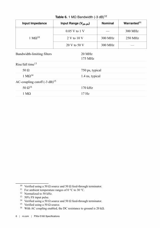
Table 6. 1 MΩ Bandwidth (-3 dB)12
Input Impedance Input Range (Vpk-pk) Nominal Warranted11
1 MΩ10
0.05 V to 1 V — 300 MHz
2 V to 10 V 300 MHz 250 MHz
20 V to 50 V 300 MHz —
Bandwidth-limiting filters 20 MHz175 MHz
Rise/fall time13
50 Ω 750 ps, typical
1 MΩ14 1.4 ns, typical
AC-coupling cutoff (-3 dB)15
50 Ω16 170 kHz
1 MΩ 17 Hz
10 Verified using a 50 Ω source and 50 Ω feed-through terminator.11 For ambient temperature ranges of 0 °C to 30 °C.12 Normalized to 50 kHz.13 50% FS input pulse.14 Verified using a 50 Ω source and 50 Ω feed-through terminator.15 Verified using a 50 Ω source.16 With AC coupling enabled, the DC resistance to ground is 20 kΩ.
6 | ni.com | PXIe-5160 Specifications

Figure 1. PXIe-5160 Step Response, 50 Ω, 1 Vpk-pk Input Range, -0.25 VProgrammable Offset, 500 ps Rising Edge, Nominal
Vol
ts0.10
–0.55
–0.50
–0.45
–0.40
–0.35
–0.30
–0.25
–0.20
–0.15
–0.10
–0.05
0.00
0.05
Time (ns)
8–2 –1 0 1 2 3 4 5 6 7
Figure 2. PXIe-5160 Step Response, 1 MΩ, 1 Vpk-pk Input Range, -0.25 VProgrammable Offset, 500 ps Rising Edge, Nominal17
Vol
ts
0.10
–0.55
–0.50
–0.45
–0.40
–0.35
–0.30
–0.25
–0.20
–0.15
–0.10
–0.05
0.00
0.05
Time (ns) 7–2 –1 0 1 2 3 4 5 6
17 Verified using a 50 Ω source and 50 Ω feed-through terminator.
PXIe-5160 Specifications | © National Instruments | 7

Figure 3. PXIe-5160 50 Ω Frequency Response, 1 Vpk-pk, 2.5 GS/s, Nominal
Frequency (Hz)1 G1 M 100 M 200 M 300 M 400 M 500 M 600 M 700 M 800 M 900 M
1
–19
–17
–15
–13
–11
–9
–7
–5
–3
–1N
orm
aliz
ed A
mpl
itude
(dB
)
Figure 4. PXIe-5160 1 MΩ Frequency Response, 1 Vpk-pk, Nominal18
Nor
mal
ized
Am
plitu
de (
dB)
1
–19
–17
–15
–13
–11
–9
–7
–5
–3
–1
Frequency (Hz)800 M1 M 100 M 200 M 300 M 400 M 500 M 600 M 700 M
18 Verified using a 50 Ω source and 50 Ω feed-through terminator.
8 | ni.com | PXIe-5160 Specifications

Figure 5. PXIe-5160 Bandwidth-Limiting Filters Frequency Response, 1 Vpk-pk, Nominal
1
–11
–10
–9
–8
–7
–6
–5
–4
–3
–2
–1
0
Frequency (Hz)10 M 100 M
Nor
mal
ized
Am
plitu
de (
dB)
Spectral Characteristics
50 Ω Spectral Characteristics
Table 7. Spurious-Free Dynamic Range (SFDR), Nominal19
Input Frequency SFDR
<10 MHz 56 dBc
≥10 MHz to ≤100 MHz 54 dBc
Table 8. Effective Number of Bits (ENOB), Nominal19
Input Frequency Input Range (Vpk-pk) ENOB
<100 MHz
0.05 V 7.1
0.1 V 7.4
0.2 V to 5 V 7.6
19 -1 dBFS input signal corrected to FS. Includes the second through the fifth harmonics. 7.2 kHzresolution bandwidth.
PXIe-5160 Specifications | © National Instruments | 9

Figure 6. PXIe-5160 Single Tone Spectrum, 2.98 dBm Input Signal at Connector, 50 Ω,1 Vpk-pk, 2.5 GS/s, 101 MHz Input Tone, Full Bandwidth, Nominal
0
–100
–90
–80
–70
–60
–50
–40
–30
–20
–10
1.25 G0 250 M 500 M 750 M 1 G
Am
plitu
de (
dBF
S)
Frequency (Hz)
1 MΩ Spectral Characteristics20
Table 9. SFDR, Nominal21
Input Frequency Input Range (Vpk-pk) SFDR
<10 MHz
0.05 V to 10 V 53 dBc
20 V 50 dBc
≥10 MHz to ≤100 MHz0.05 V to 0.5 V 53 dBc
1 V to 5 V 48 dBc
20 Verified using a 50 Ω source and 50 Ω feed-through terminator.21 -1 dBFS input signal corrected to FS. Includes the second through the fifth harmonics. 7.2 kHz
resolution bandwidth.
10 | ni.com | PXIe-5160 Specifications

Table 10. ENOB, Nominal21
Input Frequency Input Range (Vpk-pk) ENOB
<10 MHz
0.05 V 6.8
0.1 V 7.4
0.2 V to 20 V 7.6
≤100 MHz
0.05 V 6.8
0.1 V to 0.5 V 7.4
1 V to 5 V 7.1
Noise
Table 11. RMS Noise22
Input Impedance Input Range (Vpk-pk) Typical Warranted
50 Ω
0.05 V 0.26% of FS 0.3% of FS
0.1 V 0.16% of FS 0.19% of FS
0.2 V to 5 V 0.14% of FS 0.17% of FS
1 MΩ
0.05 V 0.26% of FS 0.3% of FS
0.1 V 0.16% of FS 0.19% of FS
0.2 V to 50 V 0.14% of FS 0.17% of FS
SkewChannel-to-channel skew
50 Ω to 50 Ω <25 ps, nominal
1 MΩ to 1 MΩ <125 ps, nominal
50 Ω to 1 MΩ <800 ps, nominal
22 Verified using a 50 Ω terminator connected to input.
PXIe-5160 Specifications | © National Instruments | 11
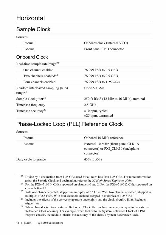
Horizontal
Sample ClockSources
Internal Onboard clock (internal VCO)
External Front panel SMB connector
Onboard ClockReal-time sample rate range23
One channel enabled 76.299 kS/s to 2.5 GS/s
Two channels enabled24 76.299 kS/s to 2.5 GS/s
Four channels enabled 76.299 kS/s to 1.25 GS/s
Random interleaved sampling (RIS)range25
Up to 50 GS/s
Sample clock jitter26 250 fs RMS (12 kHz to 10 MHz), nominal
Timebase frequency 2.5 GHz
Timebase accuracy27 ±10 ppm, typical±25 ppm, warranted
Phase-Locked Loop (PLL) Reference ClockSources
Internal Onboard 10 MHz reference
External External 10 MHz (front panel CLK INconnector) or PXI_CLK10 (backplaneconnector)
Duty cycle tolerance 45% to 55%
23 Divide by n decimation from 1.25 GS/s used for all rates less than 1.25 GS/s. For more informationabout the Sample Clock and decimation, refer to the NI High-Speed Digitizers Help.
24 For the PXIe-5160 (4 CH), supported on channels 0 and 2. For the PXIe-5160 (2 CH), supported onchannels 0 and 1.
25 With one channel enabled, stepped in multiples of 2.5 GS/s. With two channels enabled, stepped inmultiples of 2.5 GS/s. With four channels enabled, stepped in multiples of 1.25 GS/s.
26 Includes the effects of the converter aperture uncertainty and the clock circuitry jitter. Excludestrigger jitter.
27 When phase-locked to an external Reference Clock, the timebase accuracy is equal to the externalReference Clock accuracy. For example, when locked to the System Reference Clock of a PXIExpress chassis, the module inherits the accuracy of the chassis System Reference Clock.
12 | ni.com | PXIe-5160 Specifications

External Sample Clock (CLK IN, Front PanelConnector)Input voltage range, when configured as aSample Clock
-10 dBm through 16 dBm
Maximum input overload, whenconfigured as a Sample Clock
18 dBm
Impedance 50 Ω
Coupling AC
Frequency range 1.25 GHz to 2.5 GHz28
External Reference Clock In (CLK IN, Front PanelConnector)Input voltage range, when configured as aReference Clock
200 mVpk-pk to 4 Vpk-pk
Maximum input overload, whenconfigured as a Reference Clock
5 Vpk-pk with |Peaks| ≤10 V
Impedance 50 Ω
Coupling AC
Frequency range29 10 MHz
Reference Clock Out (CLK OUT, Front PanelConnector)Output impedance 50 Ω
Logic type 3.3 V CMOS
Maximum current drive ±10 mA
28 To achieve the same real-time sample rate ranges as the onboard clock, a 2.5 GHz frequency isrequired.
29 The PLL Reference Clock frequency must be accurate to ±25 ppm.
PXIe-5160 Specifications | © National Instruments | 13

TriggerSupported trigger Reference (Stop) Trigger
Trigger types EdgeDigitalImmediateHysteresisSoftware
Trigger sources
PXIe-5160 (2 CH) CH 0, CH 1, TRIG, PFI 0, PFI 1,PXI_TRIG <0..6>, and Software
PXIe-5160 (4 CH) CH 0, CH 1, CH 2, CH 3, PFI 0, PFI 1,PXI_TRIG <0..6>, and Software
Time-to-digital conversion circuit timeresolution
4 ps
Dead time 710 ns, nominal
Holdoff 6.4 ns to 27.4 s
Trigger delay From 0 to 73,786,976 seconds (28 months),nominal
Analog Trigger (Edge Trigger Type)Sources
PXIe-5160 (2 CH) CH 0, CH 1, or TRIG30
PXIe-5160 (4 CH) CH 0, CH 1, CH 2, or CH 3
Trigger filters
Low-frequency reject 150 kHz, nominal
High-frequency reject 150 kHz, nominal
Trigger sensitivity 3% of FS at ≤10 MHz, nominal
Trigger accuracy31 6% of FS at ≤10 MHz, nominal
Trigger jitter 4.7 ps, typical
30 For specifications on the TRIG input, refer to the External Trigger (TRIG, Front Panel Connector)section.
31 When the impedance settings of the triggering input and the analog input channel are the same. Formore information about functionality when using mixed impedances between input channels orexternal trigger, visit ni.com/kb and enter 5W8CFE8P.
14 | ni.com | PXIe-5160 Specifications
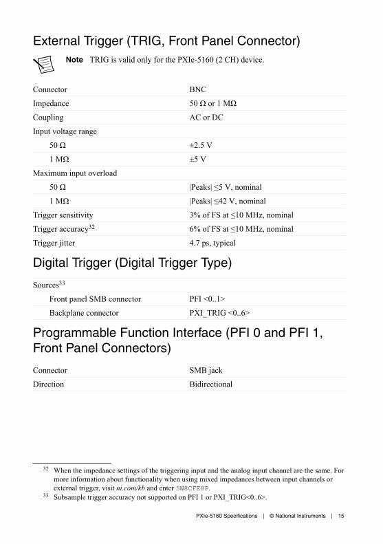
External Trigger (TRIG, Front Panel Connector)Note TRIG is valid only for the PXIe-5160 (2 CH) device.
Connector BNC
Impedance 50 Ω or 1 MΩ
Coupling AC or DC
Input voltage range
50 Ω ±2.5 V
1 MΩ ±5 V
Maximum input overload
50 Ω |Peaks| ≤5 V, nominal
1 MΩ |Peaks| ≤42 V, nominal
Trigger sensitivity 3% of FS at ≤10 MHz, nominal
Trigger accuracy32 6% of FS at ≤10 MHz, nominal
Trigger jitter 4.7 ps, typical
Digital Trigger (Digital Trigger Type)
Sources33
Front panel SMB connector PFI <0..1>
Backplane connector PXI_TRIG <0..6>
Programmable Function Interface (PFI 0 and PFI 1,Front Panel Connectors)
Connector SMB jack
Direction Bidirectional
32 When the impedance settings of the triggering input and the analog input channel are the same. Formore information about functionality when using mixed impedances between input channels orexternal trigger, visit ni.com/kb and enter 5W8CFE8P.
33 Subsample trigger accuracy not supported on PFI 1 or PXI_TRIG<0..6>.
PXIe-5160 Specifications | © National Instruments | 15

As an Input (Trigger)
Destinations Start Trigger (Acquisition Arm)Reference (Stop) TriggerAdvance Trigger
Input impedance 10 kΩ
VIH 2.0 V
VIL 0.8 V
Maximum input overload -0.5 V to 5.5 V
Maximum frequency 25 MHz
As an Output (Event)
Sources Ready for StartStart Trigger (Acquisition Arm)Ready for ReferenceArm Reference TriggerReference (Stop) TriggerEnd of RecordReady for AdvanceAdvance TriggerDone (End of Acquisition)Probe Compensation34
Output impedance 50 Ω, nominal
Logic type 3.3 V CMOS
Maximum current drive ±10 mA
Maximum frequency 25 MHz
Waveform Specifications
Onboard memory sizes35 64 MB or 2 GB
Minimum record length 1 sample
Number of pretrigger samples36 Zero up to full record length
Number of posttrigger samples36 Zero up to full record length
34 1 kHz, 50% duty cycle square wave, PFI 1 only.35 Onboard memory is shared among all enabled channels.36 Single-record and multirecord acquisitions.
16 | ni.com | PXIe-5160 Specifications

Maximum number of records in onboard memory37
64 MB 65,536
2 GB 100,000
Allocated onboard memory per record [(Record length + 448 samples) ×2 bytes/sample], rounded up to an integermultiple of 128 bytes (minimum 512 bytes)
Memory SanitizationFor information about memory sanitization, refer to the letter of volatility for your device,which is available at ni.com/manuals.
Calibration
External CalibrationExternal calibration calibrates the onboard references used in self-calibration and the externaltrigger levels. All calibration constants are stored in nonvolatile memory.
Self-CalibrationSelf-calibration is done on software command. The calibration corrects for gain, offset,triggering, and timing errors for all input ranges.
Calibration SpecificationsInterval for external calibration 2 years
Warm-up time 15 minutes
Software
Driver SoftwareDriver support for this device was first available in NI-SCOPE 4.1.
NI-SCOPE is an IVI-compliant driver that allows you to configure, control, and calibrate thePXIe-5160. NI-SCOPE provides application programming interfaces for many developmentenvironments.
37 You can exceed these numbers if you fetch records while acquiring data. For more information,refer to the NI High-Speed Digitizers Help.
PXIe-5160 Specifications | © National Instruments | 17

Application SoftwareNI-SCOPE provides programming interfaces, documentation, and examples for the followingapplication development environments:• LabVIEW• LabWindows™/CVI™
• Measurement Studio• Microsoft Visual C/C++• .NET (C# and VB.NET)
Interactive Soft Front Panel and ConfigurationThe NI-SCOPE Soft Front Panel (SFP) allows interactive control of the PXIe-5160.
Interactive control of the PXIe-5160 was first available in NI-SCOPE SFP version 4.1. TheNI-SCOPE SFP is included on the NI-SCOPE media.
NI Measurement Automation Explorer (MAX) also provides interactive configuration and testtools for the PXIe-5160. MAX is included on the NI-SCOPE media.
TClk SpecificationsYou can use the NI TClk synchronization method and the NI-TClk driver to align the Sampleclocks on any number of supported devices, in one or more chassis. For more informationabout TClk synchronization, refer to the NI-TClk Synchronization Help, which is locatedwithin the NI High-Speed Digitizers Help. For other configurations, including multichassissystems, contact NI Technical Support at ni.com/support.
Intermodule SMC Synchronization Using NI-TClk for IdenticalModulesSynchronization specifications are valid under the following conditions:• All modules are installed in one PXI Express chassis.• The NI-TClk driver is used to align the Sample clocks of each module.• All parameters are set to identical values for each module.
18 | ni.com | PXIe-5160 Specifications

• Modules are synchronized without using an external Sample clock.• Self-calibration is completed.
Note Although you can use NI-TClk to synchronize non-identical SMC-basedmodules, these specifications apply only to synchronizing identical modules.
Skew38 100 ps, nominal
Skew after manual adjustment ≤5 ps, nominal
Sample clock delay/adjustment resolution 20 fs
Related InformationFor more information about TClk synchronization, refer to the NI-TClk Synchronization Help ,which is located within the NI High-Speed Digitizers Help available at ni.com/manuals.For other configurations, including multichassis systems, contact NI Technical Support atni.com/support.
Power+3.3 VDC 2.2 A
+12 VDC 2.3 A
Total power 34.8 W
Dimensions and WeightDimensions 3U, 1 slot, PXI Express gen 1 x4 Module,
21.4 × 2.0 × 13.1 cm (8.4 × 0.8 × 5.1 in)
Weight 430 g (15 oz.)
Caution Clean the hardware with a soft, nonmetallic brush. Make sure that thehardware is completely dry and free from contaminants before returning it toservice.
EnvironmentMaximum altitude 2,000 m (800 mbar) (at 25 °C ambient
temperature)
Pollution Degree 2
Indoor use only.
38 Caused by clock and analog path delay differences. No manual adjustment performed. Tested witha NI PXIe-1082 chassis with a maximum slot-to-slot skew of 100 ps.
PXIe-5160 Specifications | © National Instruments | 19

Operating EnvironmentAmbient temperature range 0 °C to 45 °C (Tested in accordance with
IEC 60068-2-1 and IEC 60068-2-2.MeetsMIL-PRF-28800F Class 3 low temperaturelimit and MIL-PRF-28800F Class 4 hightemperature limit.)
Relative humidity range 10% to 90%, noncondensing (Tested inaccordance with IEC 60068-2-56.)
Storage EnvironmentAmbient temperature range -40 °C to 71 °C (Tested in accordance
with IEC 60068-2-1 and IEC 60068-2-2. MeetsMIL-PRF-28800F Class 3 limits.)
Relative humidity range 5% to 95%, noncondensing (Tested inaccordance with IEC 60068-2-56.)
Shock and VibrationOperating shock 30 g peak, half-sine, 11 ms pulse (Tested in
accordance with IEC 60068-2-27. MeetsMIL-PRF-28800F Class 2 limits.)
Random vibration
Operating 5 Hz to 500 Hz, 0.3 grms (Tested in accordancewith IEC 60068-2-64.)
Nonoperating 5 Hz to 500 Hz, 2.4 grms (Tested in accordancewith IEC 60068-2-64. Test profile exceeds therequirements of MIL-PRF-28800F, Class 3.)
Compliance and Certifications
SafetyThis product is designed to meet the requirements of the following electrical equipment safetystandards for measurement, control, and laboratory use:• IEC 61010-1, EN 61010-1• UL 61010-1, CSA C22.2 No. 61010-1
Note For UL and other safety certifications, refer to the product label or the OnlineProduct Certification section.
20 | ni.com | PXIe-5160 Specifications

Electromagnetic CompatibilityThis product meets the requirements of the following EMC standards for electrical equipmentfor measurement, control, and laboratory use:• EN 61326-1 (IEC 61326-1): Class A emissions; Basic immunity• EN 55011 (CISPR 11): Group 1, Class A emissions• EN 55022 (CISPR 22): Class A emissions• EN 55024 (CISPR 24): Immunity• AS/NZS CISPR 11: Group 1, Class A emissions• AS/NZS CISPR 22: Class A emissions• FCC 47 CFR Part 15B: Class A emissions• ICES-001: Class A emissions
Note In the United States (per FCC 47 CFR), Class A equipment is intended foruse in commercial, light-industrial, and heavy-industrial locations. In Europe,Canada, Australia, and New Zealand (per CISPR 11), Class A equipment is intendedfor use only in heavy-industrial locations.
Note Group 1 equipment (per CISPR 11) is any industrial, scientific, or medicalequipment that does not intentionally generate radio frequency energy for thetreatment of material or inspection/analysis purposes.
Note For EMC declarations, certifications, and additional information, refer to the Online Product Certification section.
CE Compliance This product meets the essential requirements of applicable European Directives, as follows:• 2014/35/EU; Low-Voltage Directive (safety)• 2014/30/EU; Electromagnetic Compatibility Directive (EMC)
Online Product CertificationRefer to the product Declaration of Conformity (DoC) for additional regulatory complianceinformation. To obtain product certifications and the DoC for this product, visit ni.com/certification, search by model number or product line, and click the appropriate link in theCertification column.
Environmental ManagementNI is committed to designing and manufacturing products in an environmentally responsiblemanner. NI recognizes that eliminating certain hazardous substances from our products isbeneficial to the environment and to NI customers.
For additional environmental information, refer to the Minimize Our Environmental Impactweb page at ni.com/environment. This page contains the environmental regulations and
PXIe-5160 Specifications | © National Instruments | 21

directives with which NI complies, as well as other environmental information not included inthis document.
Waste Electrical and Electronic Equipment (WEEE)EU Customers At the end of the product life cycle, all NI products must bedisposed of according to local laws and regulations. For more information abouthow to recycle NI products in your region, visit ni.com/environment/weee.
电子信息产品污染控制管理办法(中国 RoHS)中国客户 National Instruments 符合中国电子信息产品中限制使用某些有害物
质指令(RoHS)。关于 National Instruments 中国 RoHS 合规性信息,请登录
ni.com/environment/rohs_china。(For information about China RoHScompliance, go to ni.com/environment/rohs_china.)
Information is subject to change without notice. Refer to the NI Trademarks and Logo Guidelines at ni.com/trademarks forinformation on NI trademarks. Other product and company names mentioned herein are trademarks or trade names of theirrespective companies. For patents covering NI products/technology, refer to the appropriate location: Help»Patents in yoursoftware, the patents.txt file on your media, or the National Instruments Patent Notice at ni.com/patents. You can findinformation about end-user license agreements (EULAs) and third-party legal notices in the readme file for your NI product. Referto the Export Compliance Information at ni.com/legal/export-compliance for the NI global trade compliance policy and howto obtain relevant HTS codes, ECCNs, and other import/export data. NI MAKES NO EXPRESS OR IMPLIED WARRANTIES ASTO THE ACCURACY OF THE INFORMATION CONTAINED HEREIN AND SHALL NOT BE LIABLE FOR ANY ERRORS. U.S.Government Customers: The data contained in this manual was developed at private expense and is subject to the applicablelimited rights and restricted data rights as set forth in FAR 52.227-14, DFAR 252.227-7014, and DFAR 252.227-7015.
© 2013—2017 National Instruments. All rights reserved.
374020F-01 December 12, 2017