PtpTimestampUnit - NetTimeLogic GmbH · PtpTsu Reference Manual 1.0 Page 3 of 80 Overview...
80
PtpTsu Reference Manual 1.0 Page 1 of 80 Ptp Timestamp Unit Reference Manual Product Info Product Manager Sven Meier Author(s) Sven Meier Reviewer(s) - Version 1.0 Date 09.03.2018
Transcript of PtpTimestampUnit - NetTimeLogic GmbH · PtpTsu Reference Manual 1.0 Page 3 of 80 Overview...

PtpTsu Reference Manual 1.0 Page 1 of 80
PtpTimestampUnit
Reference Manual
Product Info
Product Manager Sven Meier
Author(s) Sven Meier
Reviewer(s) -
Version 1.0
Date 09.03.2018

PtpTsu Reference Manual 1.0 Page 2 of 80
Copyright Notice
Copyright © 2017 NetTimeLogic GmbH, Switzerland. All rights reserved.
Unauthorized duplication of this document, in whole or in part, by any means, is
prohibited without the prior written permission of NetTimeLogic GmbH, Switzer-
land.
All referenced registered marks and trademarks are the property of their respective
owners
Disclaimer
The information available to you in this document/code may contain errors and is
subject to periods of interruption. While NetTimeLogic GmbH does its best to
maintain the information it offers in the document/code, it cannot be held respon-
sible for any errors, defects, lost profits, or other consequential damages arising
from the use of this document/code.
NETTIMELOGIC GMBH PROVIDES THE INFORMATION, SERVICES AND PROD-
UCTS AVAILABLE IN THIS DOCUMENT/CODE "AS IS," WITH NO WARRANTIES
WHATSOEVER. ALL EXPRESS WARRANTIES AND ALL IMPLIED WARRANTIES,
INCLUDING WARRANTIES OF MERCHANTABILITY AND FITNESS FOR A PARTIC-
ULAR PURPOSE, AND NON-INFRINGEMENT OF PROPRIETARY RIGHTS ARE
HEREBY DISCLAIMED TO THE FULLEST EXTENT PERMITTED BY LAW. IN NO
EVENT SHALL NETTIMELOGIC GMBH BE LIABLE FOR ANY DIRECT, INDIRECT, IN-
CIDENTAL, CONSEQUENTIAL, SPECIAL AND EXEMPLARY DAMAGES, OR ANY
DAMAGES WHATSOEVER, ARISING FROM THE USE OR PERFORMANCE OF THIS
DOCUMENT/CODE OR FROM ANY INFORMATION, SERVICES OR PRODUCTS
PROVIDED THROUGH THIS DOCUMENT/CODE, EVEN IF NETTIMELOGIC GMBH
HAS BEEN ADVISED OF THE POSSIBILITY OF SUCH DAMAGES.
IF YOU ARE DISSATISFIED WITH THIS DOCUMENT/CODE, OR ANY PORTION
THEREOF, YOUR EXCLUSIVE REMEDY SHALL BE TO CEASE USING THE DOCU-
MENT/CODE.

PtpTsu Reference Manual 1.0 Page 3 of 80
Overview
NetTimeLogic’s PTP Timestamp Unit is an implementation of a Frame Timestamp
Unit (TSU) according to IEEE1588-2008 (PTP). It detects PTP frames on a
(R)(G)MII tap and timestamps PTP event frames based on a Counter Clock and
provides them delay compensated to a PTP Software stack (e.g. PTPd, PTP4l,
etc…). In case a Xilinx® Zynq is used it natively supports the PTP signals from the
GMAC allowing to have a PTP clock in the PL even if the PHY is connected to the
CPU only. The Timestamp Unit can work as Master and Slave. All configuration can
be written and timestamps read via an AXI4Light-Slave Register interface.
Key Features:
• PTP Timestamp Unit according to IEEE1588-2008
• PTP frame detection
• PTP event frame timestamping
• Taps path between MAC and PHY
• Synchronization accuracy: +/- 25ns
• Support for Layer 2 (Ethernet) and Layer 3 (Ip), Peer to Peer (P2P) and End
to End (E2E).
• Master and Slave support
• Full line speed
• AXI4 Light register set
• Configurable Interrupt
• PHY Delay compensation with automatic link speed detection (in driver)
• MII/GMII/RGMII Interface support (optional AXI4 stream for interconnection
to 3rd party cores)
• Suports Xilinx® Zynq GMAC PTP signals
• Timestamp resolution with 50 MHz system clock: 10ns
• Linux Driver (MAC & TSU Zynq 70xx)

PtpTsu Reference Manual 1.0 Page 4 of 80
Revision History
This table shows the revision history of this document.
Version Date Revision
0.1 15.11.2017 First draft
1.0 09.03.2018 First release
Table 1: Revision History

PtpTsu Reference Manual 1.0 Page 5 of 80
Content
1 INTRODUCTION 9
1.1 Context Overview 9
1.2 Function 10
1.3 Architecture 10
2 PTP BASICS 13
2.1 Protocol 13
2.2 Principles 13
2.2.1 PTP Nodes 16
2.2.2 Delay Mechanisms 19
2.2.3 Profiles 22
2.3 Accuracy 23
2.3.1 Timestamp accuracy 23
3 REGISTER SET 25
3.1 Register Overview 25
3.2 Register Descriptions 27
3.2.1 General TSU 27
3.2.2 Timestamp TSU 31
4 DESIGN DESCRIPTION 55
4.1 Top Level – PTP Tsu 55
4.2 Design Parts 62
4.2.1 Tsu Processor 62
4.2.2 Ethernet Interface Adapter 64
4.2.3 Registerset 67
4.3 Configuration example 71
4.3.1 AXI Configuration 71

PtpTsu Reference Manual 1.0 Page 6 of 80
4.4 Clocking and Reset Concept 72
4.4.1 Clocking 72
4.4.2 Reset 72
5 RESOURCE USAGE 74
5.1 Altera (Cyclone V) 74
5.2 Xilinx (Artix 7) 74
6 DELIVERY STRUCTURE 75
7 TESTBENCH 76
7.1 Run Testbench 77
8 REFERENCE DESIGNS 77
8.1 Xilinx: Digilent Arty Z7 78

PtpTsu Reference Manual 1.0 Page 7 of 80
Definitions
Definitions
Ordinary Clock A synchronization end node according to IEEE1588 that
can take a Master and Slave role
Transparent Clock A network node (Switch) that is IEEE1588 aware and com-
pensates network jitter
Default Profile PTP Profile according to IEEE1588
Power Profile PTP Profile according to C37.238-2011
Utility Profile PTP Profile according to IEC 61850 9-3
Timestamp Unit A module which can detect and timestamp PTP frames
Table 2: Definitions
Abbreviations
Abbreviations
AXI AMBA4 Specification (Stream and Memory Mapped)
IRQ Interrupt, Signaling to e.g. a CPU
PRP Parallel Redundancy Protocol (IEC 62439-3)
HSR High-availability Seamless Redundancy (IEC 62439-3)
PTP Precision Time Protocol (See also IEEE1588)
MAC Media Access Controller
PHY Physical Media Access Controller
OC Ordinary Clock
TC Transparent Clock
TS Timestamp
TSU Timestamp Unit
ETH Ethernet
TB Testbench
LUT Look Up Table

PtpTsu Reference Manual 1.0 Page 8 of 80
FF Flip Flop
PTP4l PTP for Linux
RAM Random Access Memory
ROM Read Only Memory
FPGA Field Programmable Gate Array
VHDL Hardware description Language for FPGA’s
Table 3: Abbreviations

PtpTsu Reference Manual 1.0 Page 9 of 80
1 Introduction
1.1 Context Overview
The PTP Timestamp Unit is meant as a co-processor handling PTP timestamps on a
network port. It taps the Media Independent Interface (MII) on the Ethernet path
between the MAC, Switch or Redundancy core and PHYs where it detects and
timestamps PTP traffic. It compensates the timestamps for the PHY delays and
generates a configurable interrupt whenever a timestamp is ready for a specific
frame type. The CPU shall use these timestamps in a PTP software stack like PTP4l,
PTPd, etc. to synchronize the clock which is the base for the timestamps (Slave) or
to distribute time (Master).
The PTP Timestamp Unit is specifically designed for Systems on Chip (SoC) where
a CPU and FPGA part are often combined on the same silicon. In addition to the MII
tap, there is also a possibility to feed PTP timestamp signals from another source
(e.g. PTP detector in a MAC), this is possible with e.g. a Xilinx® Zynq device. In this
case the frame processing is omitted and only the timestamp and register part is
used.
The PTP Timestamp Unit is designed to work in cooperation with the Counter
Clock core from NetTimeLogic (not a requirement). It contains an AXI4Light slave
for configuration, status supervision ad fetching of the timestamps from a CPU.

PtpTsu Reference Manual 1.0 Page 10 of 80
PtpTimestampUnit
CLOCKAdjustable Clock
Time &Adjustment
AX
I4 L
ite
Slav
e
CPU
AXI4L
MII RX
MII TX
EthernetPHY
MII RX
MII TX
EthernetMAC
IRQ
TSSignals
Figure 1: Context Block Diagram
1.2 Function
The PTP Timestamp Unit part is a PTP TSU according to IEEE1588-2008. It detects
PTP frames when they pass the MII and takes timestamps of PTP event frames. It
also compensates the PHY delays so the timestamps reflect the time when the PTP
frames entered or left the PHY on the cable, which is the defined timestamp point
according to IEEE1588-2008.
1.3 Architecture
The core is split up into different functional blocks for reduction of the complexity,
modularity and maximum reuse of blocks. The interfaces between the functional
blocks are kept as small as possible for easier understanding of the core.

PtpTsu Reference Manual 1.0 Page 11 of 80
AXI4 Lite Slave
REGISTERSET
MII/GMIIRX
MII/GMIITX
MII RX
MII TX
EthernetPHY
DETECTORRX
DETECTORTX
MII RX MII TX
EthernetMAC
CPU
PtpTimestampUnit
TSRX
TSTX
CLOCKAdjustable Clock
AXI4 Lite Slave
Time
Figure 2: Architecture Block Diagram
Register Set
This block allows reading timestamps and status values and writing configuration.
This block also also does the interrupt handling and the timestamp distribution to
individual frame types and directions.
Receive/Transmit Timestamper
These blocks generate a snapshot of the counter clock time when the Start of
Frame Delimiter (SFD) was detected by the Interface Adapters
Receive/Transmit Frame Detector

PtpTsu Reference Manual 1.0 Page 12 of 80
These blocks analyze the frames and extracts the PTP frame type which is pro-
vided to the Register Set.
(R)(G)MII Receive/Transmit Interface Adapter
These blocks convert the data stream from the (R)(G)MII to a 32bit AXI stream and
back form 32bit AXI stream to (R)(G)MII.

PtpTsu Reference Manual 1.0 Page 13 of 80
2 PTP Basics
2.1 Protocol
PTP means Precision Time Protocol and is standardized in IEEE1588-2008 (or also
IEC61588-Ed.2). It describes the mechanisms how to distribute time (phase and fre-
quency) precisely (sub-microsecond accuracy) over an Ethernet based, packet
based network and determines the best clock for time distribution automatically.
The principal of the protocol is based on frames that are exchanged periodically
between nodes containing timestamps of when the exchanged frames where sent
and received along with information of the clock quality of the nodes.
2.2 Principles
PTP defines a Master Slave system. In a PTP network there is only one active Mas-
ter and multiple Slaves. As already mentioned there are messages periodically ex-
changed (and timestamped) between the Master and Slave to determine and cor-
rect the offset and drift of the slave against the master and to measure the network
delay between the Slave and the Master to correct this also in the offset. For meas-
uring the delay between the Master and Slave two mechanisms are defined: Peer
To Peer (P2P) and End To End (E2E). As the names say P2P is measuring the delay
only to the next neighbor and E2E is measuring from the Slave to the Master. We
will see the advantages and disadvantages of the two mechanisms later, for now
we assume a simple setup of a Slave directly connected to a Master with nothing
then a cable in between:
PTP
MasterCable
PTP
Slav e
Figure 3: Simple setup
Now we look at the messages and calculations done for the two mechanisms: In
both cases the Master is sending a so called Announce message and so called Sync
messages to the Slave. The Master takes a timestamp T1 when it starts to send the
Sync message and depending on its capabilities puts the timestamp T1 on the fly
into the Sync message (one-step handling) or sends a second message called Sync
FollowUp which contains T1 (two-step). On the Slave side it takes a timestamp T2

PtpTsu Reference Manual 1.0 Page 14 of 80
when the Sync message is coming in. With these two timestamps (T2 and T1) the
slave can calculate an offset but the propagation delay between the master and
slave is still missing so the Slave would have a constant offset of the delay to the
Master. For calculating the delay now the two mechanisms differ:
For E2E the Slave sends a so called Delay Req message to the Master and stores
the send timestamp T3. The Master takes a timestamp T4 when it receives the De-
lay Req message and sends this timestamp T4 via a so called Delay Resp to the
Slave. Now the Slave has all four timestamps (T1-T4) to calculate the Delay accord-
ing to the calculations below.
For P2P, things work a bit different. The Slave sends a so called PDelay Req mes-
sage to its neighbor (in this case the Master) and stores the send timestamp T3.
The neighbor takes a timestamp T4 when it receives the PDelay Req message.
Then is sends a so called PDelay Resp containing T4 but and in parallel timestamps
the sending moment of the PDelay Resp with T5. Again depending on the capabili-
ties of the node it inserts the timestamp T5 on the fly into the PDelay Resp mes-
sage (one-step) or sends a second message called PDelay Resp FollowUp contain-
ing T5 (two-step). The Slave takes a timestamp T6 when it receives the PDelay
Resp message. Now the slave also has the four timestamps (T3-T6) to calculate the
Delay according to the calculations below. In contrary to the E2E mechanism also
the Master (respectively the neighbor) is also calculating the Delay the same way
as the Slave.
So for E2E the Delay calculation is based on Sync messages sent by the Master
where for P2P the Delay calculation is completely independent of Sync messages.
This means for a high accuracy delay measurement the frequency of the two
clocks have to be as close to each other as possible, where for E2E this is more im-
portant as for the P2P case. Both delay mechanisms assume a symmetrical delay
which is normally the case for Ethernet.
Once the Delay is calculated the real offset can be calculated with the two
timestamps (T1 and T2) from the Sync and the propagation delay calculated via
one of the mechanisms. With Offset correction the phase is corrected to the one
from the Master. This is done with every Sync message.
The last value that is needed to get high accuracy synchronization is the so called
Drift which is the frequency difference between the Master and Slave. Since the os-
cillators of the Master and Slave are never 100% identical the Slave will drift away
from the master during two Sync messages. To adjust the frequency the
timestamps from two Sync messages are needed (T1, T1’ and T2 and T2’). With
these four timestamps the frequency difference can be calculated and adjusted at

PtpTsu Reference Manual 1.0 Page 15 of 80
the Slave. After this both frequency and phase are adjusted and the Slave is syn-
chronized to the Master.
PTP Nodes have to be able to handle both types of messages: one-step and two-
step, but they don’t need to generate two-step frames if they are one-step capable
and vice versa.
Master Slav e
SyncSync FollowUp
Delay Req
Delay Resp
Master Slav e
SyncSync FollowUp
PDelay Req
PDelay RespPDelay Resp FollowUp
T1
T2
T3
T4
T1
T2
T3
T4
T5
T6
PDelay Req
PDelay Resp
PDelay Resp FollowUp
T3
T4
T5
T6
SyncSync FollowUp
T1'
T2'
SyncSync FollowUp
T1'
T2'
E2E P2P
AnnounceAnnounce
Figure 4: Message exchange simple setup
𝐷𝑒𝑙𝑎𝑦 =(𝑇4 − 𝑇1) − (𝑇3 − 𝑇2)
2 𝐷𝑒𝑙𝑎𝑦 =
(𝑇6 − 𝑇3) − (𝑇5 − 𝑇4)
2
𝑂𝑓𝑓𝑠𝑒𝑡 = (𝑇2 − 𝑇1) − 𝐷𝑒𝑙𝑎𝑦
𝐷𝑟𝑖𝑓𝑡 =(𝑇2′ − 𝑇2) − (𝑇1′ − 𝑇1)
(𝑇1′ − 𝑇1)

PtpTsu Reference Manual 1.0 Page 16 of 80
In this example one Master was connected to exactly one Slave. In a normal setup
there are many Slaves and one Master. PTP is self-organizing, which means it
chooses the best available Master in a Network and all Slaves are then synchroniz-
ing to this Master. In a PTP network there are normally multiple Master capable
nodes, therefore the Announce messages exist. With the Announce messages the
Master capable device announces its clock quality in the network as long as no An-
nounce message from a better node is received or a timeout occurred. This way in
a steady state only one node is sending Announce messages and therefor is the
Master in the network. Also the node which is sending Announce messages has to
send Sync messages since it is the Master in the network. The comparison of the
clock quality parameters and the state machine is defined in the Best Master Clock
(BMC) algorithm.
2.2.1 PTP Nodes
IEEE1588 defines seven types of PTP nodes which all have different functions in a
PTP network
2.2.1.1 Ordinary Clock (OC)
An Ordinary Clock (OC) is defined as a PTP clock with a single PTP port. It can op-
erate either as a Master or Slave in the PTP network. The mode is selected via the
BMC algorithm. Ordinary Clocks are the most common node type in a PTP network
as they are generally used as end-nodes within a network requiring synchronization
between each other. One of the OCs will act as a Master and all other ones will stay
in Slave mode. If the current Master goes away one of the OCs will take over the
Master role and synchronize the other nodes.
2.2.1.2 Grandmaster Clock (GM)
A Grandmaster Clock (GM) is defined as a PTP Ordinary Clock with either an exter-
nal time source (GPS, IRIG) or a very high accuracy time (ATOM). It can only act as
a Master in the PTP network and will win the Master role according the BMC. In the
case that more than one Grandmaster is connected to the same PTP network the
one which is worse according to the BMC will go in a Passive state where it remains
as long as the Master is active. This is used in the case of backup Grandmasters.
2.2.1.3 Slave Only Clock (SC)
A Slave Only Clock (SC) is defined as a PTP Ordinary Clock which can only act as a
Slave in the PTP network and will never win the Master role according the BMC; it
PtpTsu Reference Manual 1.0 Page 17 of 80
will therefor also never send Announce Messages. Slave Only Clocks are always
end nodes, so if no Master is available in the network they will be unsynchronized.
Since they don’t really participate in the BMC selection a very lightweight imple-
mentation of slave only clocks is possible.
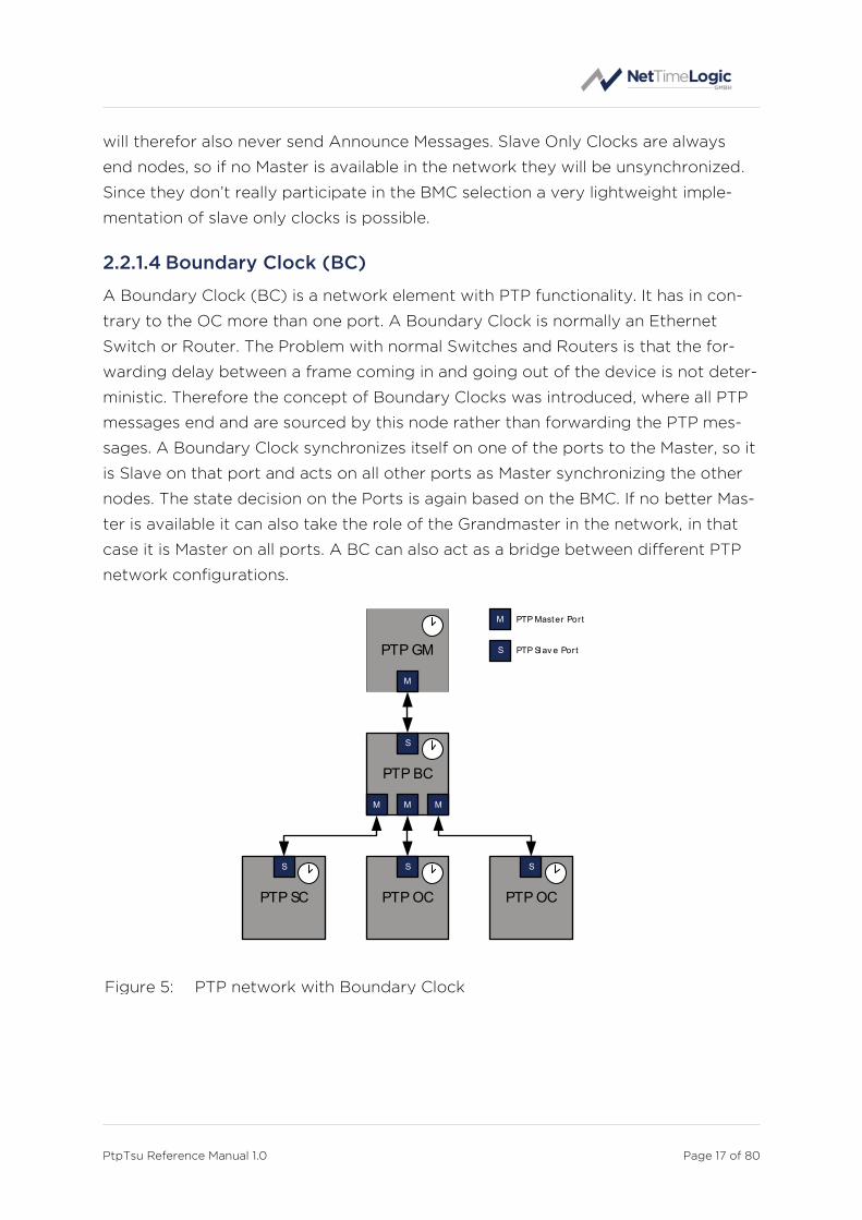
2.2.1.4 Boundary Clock (BC)
A Boundary Clock (BC) is a network element with PTP functionality. It has in con-
trary to the OC more than one port. A Boundary Clock is normally an Ethernet
Switch or Router. The Problem with normal Switches and Routers is that the for-
warding delay between a frame coming in and going out of the device is not deter-
ministic. Therefore the concept of Boundary Clocks was introduced, where all PTP
messages end and are sourced by this node rather than forwarding the PTP mes-
sages. A Boundary Clock synchronizes itself on one of the ports to the Master, so it
is Slave on that port and acts on all other ports as Master synchronizing the other
nodes. The state decision on the Ports is again based on the BMC. If no better Mas-
ter is available it can also take the role of the Grandmaster in the network, in that
case it is Master on all ports. A BC can also act as a bridge between different PTP
network configurations.
PTP GM
PTP OCPTP SC PTP OC
PTP BC
M
S
M M M
S S S
M
S
PTP Master Port
PTP Slav e Port
Figure 5: PTP network with Boundary Clock

PtpTsu Reference Manual 1.0 Page 18 of 80
2.2.1.5 Transparent Clock (TC)
A Transparent Clock (TC) is as the Boundary Clock a network element with PTP
functionality. A Transparent Clock is normally an Ethernet Switch or another Net-
work element with more than one port. In contrary to the Boundary Clock it is
stateless, so no port is in a Master or Slave state. To overcome the mentioned
problem of non-deterministic forwarding delays in the Switch it measure the resi-
dence time of a PTP message in the Switch and adds this value to a so called Cor-
rection Field within the PTP messages. So for the Slave a Transparent Clock is not
visible, it just gets the correction values which it has to take into account in the De-
lay, Offset and Drift calculations. The Transparent clock comes in different flavors:
E2E one-step or two-step TC and P2P one-step or two-step TC. To simplify the im-
plementations of TCs only one-step TCs are considered in this description. A one-
step TC can put the residence time of a PTP message on the fly into the message.
This residence time has then be taken into account when calculating Delays and
Offset so the residence time is falling out of the calculation and only the cable de-
lays are remaining. An advantage of the TC over the BC is that no cascaded servo
loops are introduced which makes deeper hierarchies possible without making the
chain unstable Also reaction time of the system significantly increases since for
each hierarchy you don’t have to wait until the higher hierarchy has been synchro-
nized.
PTP GM
PTP OCPTP SC PTP OC
PTP TC
M
T
T T T
S S S
M
S
T
PTP Master Port
PTP Slav e Port
PTP Transparent Port
Figure 6: PTP network with Transparent Clock

PtpTsu Reference Manual 1.0 Page 19 of 80
2.2.1.6 Timestamp Unit (HC)
A Timestamp Unit (HC) is a combination of a Transparent and Ordinary Clock.
Timestamp Units are often used in Daisy-Chains. In a Daisy-Chain a three port TC is
used, two ports are used for the forwarding path on the Daisy-Chain and one is
used as the uplink to the CPU and OC.
2.2.1.7 Management Node (MN)
A Management Node (MN) does not take part in the synchronization and BMC of
the PTP network. It sends PTP Management messages to the nodes to supervise
the state of the PTP network. All PTP nodes have to response to PTP Management
messages according to the standard, however a lot of the PTP nodes don’t support
PTP Management anymore because of security reasons, therefore PTP Manage-
ment nodes are not widely used.
2.2.2 Delay Mechanisms
Measuring the delay is one of the important mechanisms in PTP. In general all net-
work nodes (Switches/Routers) shall be PTP aware (BC or TC) because of the
mentioned non-determinism of message forwarding in Switches and Routers. How-
ever for E2E Delay measurements also standard Switches could be in the network,
but this requires a lot of statistics and high message rates to achieve sub-microsec-
ond accuracy (and is not always possible).
For the P2P Delay mechanism only PTP aware Switches/Routers are allowed,
breaking this rule will break the synchronization! For the next chapters only PTP
aware nodes are considered in the network. Only one delay mechanism per PTP
segment is allowed and cannot be mixed. Special Boundary Clocks exist which can
run different delay mechanisms per PTP segment (ports belonging to one network,
in best case per port).
2.2.2.1 E2E
In End to End (E2E) Delay measurement the Slave measures the whole path delay
to the next Master port.

PtpTsu Reference Manual 1.0 Page 20 of 80
PTP GM
PTP OCPTP SC PTP OC
PTP BC
M
S
M M M
S S S
M
S
PTP Master Port
PTP Slav e Port
Sy nc & Announce
Delay Resp
Delay Req PTP GM
PTP OCPTP SC PTP OC
M
T
T T T
S S S
M
S
T
PTP Master Port
PTP Slav e Port
PTP Transparent Port
Sy nc & Announce
Delay Resp
Delay Req
PTP TC
Figure 7: E2E Delay measurement with BC and TC
In the case of a network with a BC this means the Slaves measure the path directly
to the BC. The BC itself measures the Delay to the Grandmaster and synchronizes
to it. Since the Sync, Announce and Delay messages always end and are sourced at
the BC, there is no correction needed in the Messages. Each Master port only re-
ceives the Delay Req messages from the Slave directly connected to it and each
Slave port only receives Delay Resp for his Delay Req (this is not the case if non
PTP aware Switches/Routers are used) from the BC.
In the case of a network with an E2E TC, things look differently. Since the TC is
stateless it just forwards all PTP messages according to switching rules (all PTP
messages in this case are L2 multicast messages) to all other ports except the port
the message came from. This means that the Grandmaster receives the Delay Req
messages from all three Slaves and has to answer all of the with a Delay Resp mes-
sage. Also a Slave receives all Delay Req messages from all the other Slaves as well
as all Delay Resp messages from the Master, means the Delay Resp message for his
Delay Req message but also the Delay Resp messages as response to the other
Slaves Delay Req messages. In a large-scale network this produces quite some un-
necessary network load because of the other Slaves Delay messages at the Slaves
and quite some CPU and network load on the Master because it has to answer all
Slaves Delay Req message. The TC corrects the residence time of the Sync and De-
lay Req messages directly in the Correction Field of these messages.
A Slave can subtract this correction value from its Delay so the only things that re-
main are the cable delays.

PtpTsu Reference Manual 1.0 Page 21 of 80
2.2.2.2 P2P
In Peer to Peer (P2P) Delay measurement each PTP node measures the delay only
to its direct neighbor independent of it’s the node type and port state. So the Slave
never knows the whole delay to the master.
PTP GM
PTP OCPTP SC PTP OC
PTP BC
M
S
M M M
S S S
M
S
PTP Master Port
PTP Slav e Port
Sy nc & Announce
PDelay Resp
PDelay Req PTP GM
PTP OCPTP SC PTP OC
M
T
T T T
S S S
M
S
T
PTP Master Port
PTP Slav e Port
PTP Transparent Port
Sy nc & Announce
PDelay Resp
PDelay Req
PTP TC
Figure 8: P2P Delay measurement with BC and TC
In the case of a network with a BC this means not only the Slaves but also the
Grandmaster measure the path directly to the BC. The BC itself measures the Delay
to the Grandmaster and synchronizes to it, and it also measures the Delay to all
other nodes connected to it. Since the Sync, Announce and Delay messages always
end and are sourced at the BC, there is no correction needed in the Messages. Each
port only receives the PDelay Req and PDelay Resp messages from the node di-
rectly connected to it but this also means that PDelay Req messages have to be
answered with PDelay Resp messages by each port in the network participating in
PTP.
In the case of a network with a P2P TC, things work a bit differently. Unlike in the
E2E case the TC measures in P2P like the BC the Delay to all other nodes (Slaves
and Master) and answers all PDelay Req messages on each port. Since the PDelay
messages have a Link-Local destination MAC address they will not be passed
through a Switch or Router. Therefore similar as with a BC the PDelay messages
end at and are sourced by the TC. The difference to E2E delay message handling
gets clear when it comes to Sync messages. When a Sync message is received at
the TC the Delay measured on this specific port is added to the Correction Field of
this Sync message. When the frame is leaving the TC it adds the residence also to
the Correction Field and forwards it to the Slave. So for a Slave the whole delay of

PtpTsu Reference Manual 1.0 Page 22 of 80
the Frame up to its last neighbor is summed up in the Correction field. Together
with its own measured delay it gets the whole Delay that this frame has faced in
the transmission from the Master to the Slave port.
A Slave can subtract this Correction together with its Delay value from its T2
timestamp and gets from there the Offset from the master.
2.2.2.3 E2E vs. P2P
They main advantage of E2E is that it works with non-PTP aware Switches (legacy
or not feasible), which is often the case in Telecom or Office environments and that
an E2E TC can be implemented very easily. Other than that E2E delay measure-
ments has only drawbacks compared to P2P: E2E creates more network load and
CPU load on the Master which means it doesn’t scale well. E2E cannot react fast on
Master switches, since it first has to measure the whole Delay chain again, where
with P2P an immediate switchover can happen because of pre-measured delays
and summing up of Delay and Residence values in the case of TCs. Also E2E meas-
urement is not the preferred mechanism for Redundancy protocols like HSR and
PRP and Ring topologies because this would require that Sync and Delay messages
take the same way which is not always given.
So in general, whenever possible P2P delay measurement is the preferred mecha-
nism.
2.2.3 Profiles
PTP comes in different flavors (Profiles), depending on the environment it shall be
used in. Profiles define communication medium mappings (Ethernet, Profinet, and
IR etc.), message rates, the delay mechanisms, default values of datasets and
sometimes much more:
• Default Profile uses either Layer 2 or 3 with Multicast and either E2E or P2P
Delay mechanism
• Power Profile uses Layer 2 with Multicast and P2P Delay mechanism and ad-
ditional TLV
• Utility Profile uses also Layer 2 with Multicast and P2P Delay mechanism in
combination with Redundancy Protocols like HSR or PRP
• …
There are many other Profiles with other feature sets and mappings. Some Profiles
are subsets of the Default Profile and compatible, some are supersets and therefor
incompatible with other Profiles. This makes interoperability difficult.

PtpTsu Reference Manual 1.0 Page 23 of 80
So if you want to use PTP, first it is important to choose the right Profile for your
application and second to make sure that all devices in the network support the
chosen Profile
2.3 Accuracy
The accuracy of the synchronization depends highly on the precision of the
timestamps.
They should reflect the send and receive time as precise as possible. The slave's
Offset and Delay calculations are based on the difference of timestamps taken at
two different places. Therefore, the two clocks should use the same scale, i.e. the
same frequency.
This is achieved by Drift compensation: the Slave’s clock rate is accelerated or
slowed down by a control loop. A slightly different frequency will degrade the re-
sult.
It is assumed that the propagation Delay is the same for both directions. At a first
glance, this is the case with an Ethernet link.
In the long run, conditions may change due to reconfiguration or environmental
conditions (temperature).
How fast the clocks can react depends on the frequency of sync and delay meas-
urement and the dynamic behavior of the servos controlling the Slave clock.
To sum things up, the achievable accuracy depends on:
• Timestamp accuracy
• Clock stability
• Sync interval
• Clock control loop characteristics
• Drift compensated clocks (i.e. adjusted time base in Master and Slave clocks)
• The communication channel symmetry (i.e. same delay in both directions
and constant over a longer period of time)
2.3.1 Timestamp accuracy
As just stated timestamp accuracy is the key to high accuracy. PTP timestamp sup-
port can be implemented at different layers with decrease in accuracy in the higher
layers. For this solution a timestamp point between MAC and PHY (on MII) was
chosen to get the best possible accuracy without implementing PHY functionality
This interface is perfect for the use of FPGAs since it is a strictly digital interface,

PtpTsu Reference Manual 1.0 Page 24 of 80
standardized and has only a low frequency requirement. This interface can either
be intercept if one-step support is desired or passively listened if two-step support
is sufficient. For this implementation the FPGA is taping the Path between MAC
and PHY.
PHY
MAC
Driv er
Netw ork Stack
Appl icat ion
Inaccuracy
Laye
r
NetTimeLogic
Figure 9: Timestamp Incauracy in the different Layers
Not only PTP timestamping but also frame generation, handling and servo loops
can be done in different stages. Often a solution is to have the timestamping at a
very low layer and all other things in the application layer which implies that a MAC,
CPU and Operating System (e.g. Linux) with Drivers, a Network Stack and a PTP
application (e.g. PTP4l) is in place. This is exactly the setup this IP core is build for.

PtpTsu Reference Manual 1.0 Page 25 of 80
3 Register Set
This is the register set of the PTP Timestamp Unit. It is accessible via AXI4 Light Memory Mapped. All registers are 32bit wide, no
burst access, no unaligned access, no byte enables, no timeouts are supported. Register address space is not contiguous. Register
addresses are only offsets in the memory area where the core is mapped in the AXI inter connects. Non existing register access in
the mapped memory area is answered with a slave decoding error.
3.1 Register Overview
Registerset Overview
Name Description Offset Access
Ptp TsuControl Reg TSU Enable Control Register 0x00000000 RW
Ptp TsuStatus Reg TSU Error Status Register 0x00000004 WC
Ptp TsuVersion Reg TSU Version Register 0x0000000C RO
Ptp TsuTsControl Reg TSU TS Control Register 0x00000100 RW
Ptp TsuTsStatus Reg TSU TS Status Register 0x00000104 WC
Ptp TsuTsIrq Reg TSU TS Interrupt Register 0x00000110 WC
Ptp TsuTsIrqMask Reg TSU TS Interrupt Mask Register 0x00000114 RW
Ptp TsuTsDelayReqRxL Reg TSU TS DelayReqRX Low Register 0x00000120 RO
Ptp TsuTsDelayReqRxH Reg TSU TS DelayReqRX High Register 0x00000124 RO
Ptp TsuTsDelayReqTxL Reg TSU TS DelayReqTX Low Register 0x00000128 RO
Ptp TsuTsDelayReqTxH Reg TSU TS DelayReqTX High Register 0x0000012C RO
Ptp TsuTsPDelayReqRxL Reg TSU TS PDelayReqRX Low Register 0x00000130 RO
Ptp TsuTsPDelayReqRxH Reg TSU TS PDelayReqRX High Register 0x00000134 RO
Ptp TsuTsPDelayReqTxL Reg TSU TS PDelayReqTX Low Register 0x00000138 RO
Ptp TsuTsPDelayReqTxH Reg TSU TS PDelayReqTX High Register 0x0000013C RO
Ptp TsuTsPDelayRespRxL Reg TSU TS PDelayRespRX Low Register 0x00000140 RO
PtpTsu Reference Manual 1.0 Page 26 of 80
Ptp TsuTsPDelayRespRxH Reg TSU TS PDelayRespRX High Register 0x00000144 RO
Ptp TsuTsPDelayRespTxL Reg TSU TS PDelayRespTX Low Register 0x00000148 RO
Ptp TsuTsPDelayRespTxH Reg TSU TS PDelayRespTX High Register 0x0000014C RO
Ptp TsuTsSyncRxL Reg TSU TS SyncRX Low Register 0x00000150 RO
Ptp TsuTsSyncRxH Reg TSU TS SyncRX High Register 0x00000154 RO
Ptp TsuTsSyncTxL Reg TSU TS SyncTX Low Register 0x00000158 RO
Ptp TsuTsSyncTxH Reg TSU TS SyncTX High Register 0x0000015C RO
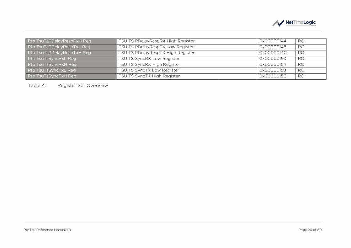
Table 4: Register Set Overview

PtpTsu Reference Manual 1.0 Page 27 of 80
3.2 Register Descriptions
3.2.1 General TSU
3.2.1.1 PTP TSU Control Register
Used for general control over the PTP Timestamp Unit, all configurations on the core shall only be done when disabled.
The link speed bit are either read only (all except TsuExt) or must be set to get the correct delay compensation
Ptp TsuControl Reg
Reg Description
31 30 29 28 27 26 25 24 23 22 21 20 19 18 17 16 15 14 13 12 11 10 9 8 7 6 5 4 3 2 1 0
-
100
0_
MB
IT
100
_M
BIT
-
EN
AB
LE
RO RW RW RO RW
Reset: 0x00000100
Offset: 0x0000
Name Description Bits Access
- Reserved, read 0 Bit:31:10 RO
1000_MBIT "1x" = 1000 Mbit, "01" = 100 Mbit, "00" = 10 Mbit Bit: 9 RW

PtpTsu Reference Manual 1.0 Page 28 of 80
100_MBIT (can only be written in TsuExt) Bit: 8 RW
- Reserved, read 0 Bit:7:1 RO
ENABLE Enable Bit: 0 RW

PtpTsu Reference Manual 1.0 Page 29 of 80
3.2.1.2 PTP TSU Status Register
Shows the current status of the PTP Timestamp Unit. It shows the state of the reference time, wheter it made a timejump or the
time is not counting at all
Ptp TsuStatus Reg
Reg Description
31 30 29 28 27 26 25 24 23 22 21 20 19 18 17 16 15 14 13 12 11 10 9 8 7 6 5 4 3 2 1 0
-
TIM
E_
JU
MP
TIM
E_
INV
AL
ID
RO WC WC
Reset: 0x00000000
Offset: 0x0004
Name Description Bits Access
- Reserved, read 0 Bit:31:2 RO
TIME_JUMP Time Jump (sticky) Bit: 1 WC
TIME_INVALID Time Invalid (sticky) Bit: 0 WC

PtpTsu Reference Manual 1.0 Page 30 of 80
3.2.1.3 PTP TSU Version Register
Version of the IP core, even though it is seen as a 32bit value, bits 31 down to 24 represent the major, bits 23 down to 16 the minor
and bits 15 down to 0 the build numbers.
Ptp TsuVersion Reg
Reg Description
31 30 29 28 27 26 25 24 23 22 21 20 19 18 17 16 15 14 13 12 11 10 9 8 7 6 5 4 3 2 1 0
VE
RS
ION
RO
Reset: 0xXXXXXXXX
Offset: 0x000C
Name Description Bits Access
VERSION Version of the IP core Bit: 31:0 RO

PtpTsu Reference Manual 1.0 Page 31 of 80
3.2.2 Timestamp TSU
The Timestamp unit only supports timestamping for PTP event messages (the ones that require a timestamp).
3.2.2.1 PTP TSU TS Control Register
Enable and disable specific frame type and direction timestamping
Ptp TsuTsControl Reg
Reg Description
31 30 29 28 27 26 25 24 23 22 21 20 19 18 17 16 15 14 13 12 11 10 9 8 7 6 5 4 3 2 1 0
-
SY
NC
_T
X
SY
NC
_R
X
PD
EL
AY
_R
ES
P_
TX
PD
EL
AY
_R
ES
P_
RX
PD
EL
AY
_R
EQ
_T
X
PD
EL
AY
_R
EQ
_R
X
DE
LA
Y_
RE
Q_
TX
DE
LA
Y_
RE
Q_
RX
RO RW
RW
RW
RW
RW
RW
RW
RW
Reset: 0x00000000
Offset: 0x0100
Name Description Bits Access
- Reserved, read 0 Bit:31:8 RO
SYNC_TX Timestamp Enable Bit: 7 RW
SYNC_RX Timestamp Enable Bit: 6 RW
PDELAY_RESP_TX Timestamp Enable Bit: 5 RW
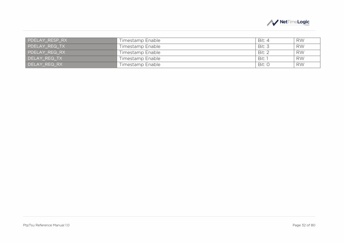
PtpTsu Reference Manual 1.0 Page 32 of 80
PDELAY_RESP_RX Timestamp Enable Bit: 4 RW
PDELAY_REQ_TX Timestamp Enable Bit: 3 RW
PDELAY_REQ_RX Timestamp Enable Bit: 2 RW
DELAY_REQ_TX Timestamp Enable Bit: 1 RW
DELAY_REQ_RX Timestamp Enable Bit: 0 RW

PtpTsu Reference Manual 1.0 Page 33 of 80
3.2.2.2 PTP TSU TS Status Register
This is used to check if a timestamp was taken or if a timestamp error is pending. Timestamping is automatically disabled until the
corresponding valid flag is cleared by writing a ‘1’ to the bit. A timestamp error signals that a timestamp should have been taken
while the old timestamp was not cleared yet.
Ptp TsuTsStatus Reg
Reg Description
31 30 29 28 27 26 25 24 23 22 21 20 19 18 17 16 15 14 13 12 11 10 9 8 7 6 5 4 3 2 1 0
-
SY
NC
_T
X_
ER
R
SY
NC
_R
X_
ER
R
PD
EL
AY
_R
ES
P_
TX
_E
RR
PD
EL
AY
_R
ES
P_
RX
_E
RR
PD
EL
AY
_R
EQ
_T
X_
ER
R
PD
EL
AY
_R
EQ
_R
X_
ER
R
DE
LA
Y_
RE
Q_
TX
_E
RR
DE
LA
Y_
RE
Q_
RX
_E
RR
-
SY
NC
_T
X
SY
NC
_R
X
PD
EL
AY
_R
ES
P_
TX
PD
EL
AY
_R
ES
P_
RX
PD
EL
AY
_R
EQ
_T
X
PD
EL
AY
_R
EQ
_R
X
DE
LA
Y_
RE
Q_
TX
DE
LA
Y_
RE
Q_
RX
RO WC WC WC WC WC WC WC WC RO WC WC WC WC WC WC WC WC
Reset: 0x00000000
Offset: 0x0104
Name Description Bits Access
- Reserved, read 0 Bit:31:24 RO
SYNC_TX_ERR Timestamp Error (sticky) Bit: 23 WC
SYNC_RX_ERR Timestamp Error (sticky) Bit: 22 WC
PDELAY_RESP_TX_ERR Timestamp Error (sticky) Bit: 21 WC
PDELAY_RESP_RX_ERR Timestamp Error (sticky) Bit: 20 WC

PtpTsu Reference Manual 1.0 Page 34 of 80
PDELAY_REQ_TX_ERR Timestamp Error (sticky) Bit: 19 WC
PDELAY_REQ_RX_ERR Timestamp Error (sticky) Bit: 18 WC
DELAY_REQ_TX_ERR Timestamp Error (sticky) Bit: 17 WC
DELAY_REQ_RX_ERR Timestamp Error (sticky) Bit: 16 WC
- Reserved, read 0 Bit:15:8 RO
SYNC_TX Timestamp Valid Bit: 7 WC
SYNC_RX Timestamp Valid Bit: 6 WC
PDELAY_RESP_TX Timestamp Valid Bit: 5 WC
PDELAY_RESP_RX Timestamp Valid Bit: 4 WC
PDELAY_REQ_TX Timestamp Valid Bit: 3 WC
PDELAY_REQ_RX Timestamp Valid Bit: 2 WC
DELAY_REQ_TX Timestamp Valid Bit: 1 WC
DELAY_REQ_RX Timestamp Valid Bit: 0 WC

PtpTsu Reference Manual 1.0 Page 35 of 80
3.2.2.3 PTP TSU TS Interrupt Register
This signals for which frame type an interrupt is pending. This is a AND combination with the mask register. Write a ‘1’ to clear a
specific interrupt
Ptp TsuTsIrq Reg
Reg Description
31 30 29 28 27 26 25 24 23 22 21 20 19 18 17 16 15 14 13 12 11 10 9 8 7 6 5 4 3 2 1 0
-
SY
NC
_T
X
SY
NC
_R
X
PD
EL
AY
_R
ES
P_
TX
PD
EL
AY
_R
ES
P_
RX
PD
EL
AY
_R
EQ
_T
X
PD
EL
AY
_R
EQ
_R
X
DE
LA
Y_
RE
Q_
TX
DE
LA
Y_
RE
Q_
RX
RO WC WC WC WC WC WC WC WC
Reset: 0x00000000
Offset: 0x0110
Name Description Bits Access
- Reserved, read 0 Bit:31:8 RO
SYNC_TX Timestamp Interrupt Bit: 7 WC
SYNC_RX Timestamp Interrupt Bit: 6 WC
PDELAY_RESP_TX Timestamp Interrupt Bit: 5 WC
PDELAY_RESP_RX Timestamp Interrupt Bit: 4 WC
PDELAY_REQ_TX Timestamp Interrupt Bit: 3 WC
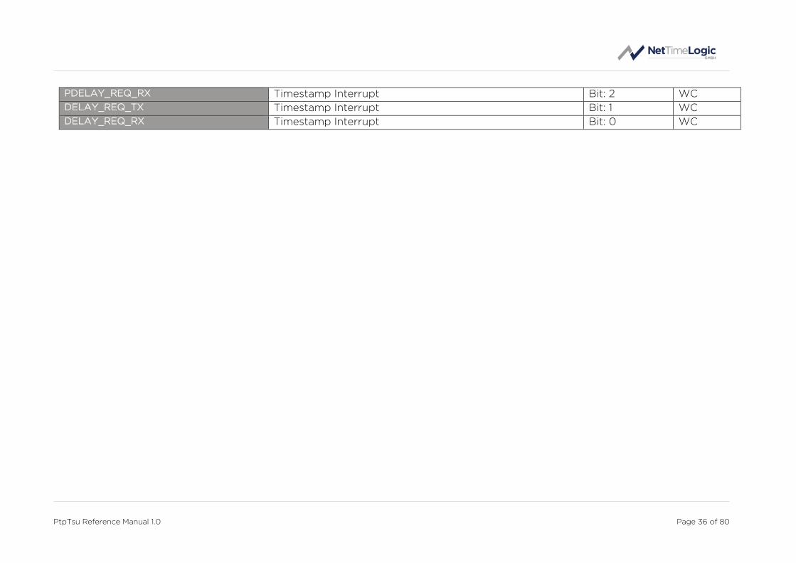
PtpTsu Reference Manual 1.0 Page 36 of 80
PDELAY_REQ_RX Timestamp Interrupt Bit: 2 WC
DELAY_REQ_TX Timestamp Interrupt Bit: 1 WC
DELAY_REQ_RX Timestamp Interrupt Bit: 0 WC

PtpTsu Reference Manual 1.0 Page 37 of 80
3.2.2.4 PTP TSU TS Interrupt Mask Register
Used to enable and disable interrupts based on the frame type and direction. This doesn not enable or disable timestamping it only
masks whether the interrupt should be set for a specific frame type and direction.
Ptp TsuTsIrqMask Reg
Reg Description
31 30 29 28 27 26 25 24 23 22 21 20 19 18 17 16 15 14 13 12 11 10 9 8 7 6 5 4 3 2 1 0
-
SY
NC
_T
X
SY
NC
_R
X
PD
EL
AY
_R
ES
P_
TX
PD
EL
AY
_R
ES
P_
RX
PD
EL
AY
_R
EQ
_T
X
PD
EL
AY
_R
EQ
_R
X
DE
LA
Y_
RE
Q_
TX
DE
LA
Y_
RE
Q_
RX
RO RW RW RW RW RW RW RW RW
Reset: 0x00000000
Offset: 0x0114
Name Description Bits Access
- Reserved, read 0 Bit:31:8 RO
SYNC_TX Timestamp Interrupt Enable Bit: 7 RW
SYNC_RX Timestamp Interrupt Enable Bit: 6 RW
PDELAY_RESP_TX Timestamp Interrupt Enable Bit: 5 RW
PDELAY_RESP_RX Timestamp Interrupt Enable Bit: 4 RW
PDELAY_REQ_TX Timestamp Interrupt Enable Bit: 3 RW

PtpTsu Reference Manual 1.0 Page 38 of 80
PDELAY_REQ_RX Timestamp Interrupt Enable Bit: 2 RW
DELAY_REQ_TX Timestamp Interrupt Enable Bit: 1 RW
DELAY_REQ_RX Timestamp Interrupt Enable Bit: 0 RW

PtpTsu Reference Manual 1.0 Page 39 of 80
3.2.2.5 PTP TSU TS DelayReq RX Timestamp Value Low Register
Timestamp nanosecond part
Ptp TsuTsDelayReqRxL Reg
Reg Description
31 30 29 28 27 26 25 24 23 22 21 20 19 18 17 16 15 14 13 12 11 10 9 8 7 6 5 4 3 2 1 0
TIM
E_
NS
RO
Reset: 0x00000000
Offset: 0x0120
Name Description Bits Access
TIME_NS Snapshoted Time Nanosecond Bit: 31:0 RO

PtpTsu Reference Manual 1.0 Page 40 of 80
3.2.2.6 PTP TSU TS DelayReq RX Timestamp Value High Register
Timestamp second part
Ptp TsuTsDelayReqRxH Reg
Reg Description
31 30 29 28 27 26 25 24 23 22 21 20 19 18 17 16 15 14 13 12 11 10 9 8 7 6 5 4 3 2 1 0
TIM
E_
S
RO
Reset: 0x00000000
Offset: 0x0124
Name Description Bits Access
TIME_S Snapshoted Time Second Bit: 31:0 RO

PtpTsu Reference Manual 1.0 Page 41 of 80
3.2.2.7 PTP TSU TS DelayReq TX Timestamp Value Low Register
Timestamp nanosecond part
Ptp TsuTsDelayReqTxL Reg
Reg Description
31 30 29 28 27 26 25 24 23 22 21 20 19 18 17 16 15 14 13 12 11 10 9 8 7 6 5 4 3 2 1 0
TIM
E_
NS
RO
Reset: 0x00000000
Offset: 0x0128
Name Description Bits Access
TIME_NS Snapshoted Time Nanosecond Bit: 31:0 RO

PtpTsu Reference Manual 1.0 Page 42 of 80
3.2.2.8 PTP TSU TS DelayReq TX Timestamp Value High Register
Timestamp second part
Ptp TsuTsDelayReqTxH Reg
Reg Description
31 30 29 28 27 26 25 24 23 22 21 20 19 18 17 16 15 14 13 12 11 10 9 8 7 6 5 4 3 2 1 0
TIM
E_
S
RO
Reset: 0x00000000
Offset: 0x012C
Name Description Bits Access
TIME_S Snapshoted Time Second Bit: 31:0 RO

PtpTsu Reference Manual 1.0 Page 43 of 80
3.2.2.9 PTP TSU TS PDelayReq RX Timestamp Value Low Register
Timestamp nanosecond part
Ptp TsuTsPDelayReqRxL Reg
Reg Description
31 30 29 28 27 26 25 24 23 22 21 20 19 18 17 16 15 14 13 12 11 10 9 8 7 6 5 4 3 2 1 0
TIM
E_
NS
RO
Reset: 0x00000000
Offset: 0x0130
Name Description Bits Access
TIME_NS Snapshoted Time Nanosecond Bit: 31:0 RO

PtpTsu Reference Manual 1.0 Page 44 of 80
3.2.2.10 PTP TSU TS PDelayReq RX Timestamp Value High Register
Timestamp second part
Ptp TsuTsPDelayReqRxH Reg
Reg Description
31 30 29 28 27 26 25 24 23 22 21 20 19 18 17 16 15 14 13 12 11 10 9 8 7 6 5 4 3 2 1 0
TIM
E_
S
RO
Reset: 0x00000000
Offset: 0x0134
Name Description Bits Access
TIME_S Snapshoted Time Second Bit: 31:0 RO

PtpTsu Reference Manual 1.0 Page 45 of 80
3.2.2.11 PTP TSU TS PDelayReq TX Timestamp Value Low Register
Timestamp nanosecond part
Ptp TsuTsPDelayReqTxL Reg
Reg Description
31 30 29 28 27 26 25 24 23 22 21 20 19 18 17 16 15 14 13 12 11 10 9 8 7 6 5 4 3 2 1 0
TIM
E_
NS
RO
Reset: 0x00000000
Offset: 0x0138
Name Description Bits Access
TIME_NS Snapshoted Time Nanosecond Bit: 31:0 RO

PtpTsu Reference Manual 1.0 Page 46 of 80
3.2.2.12 PTP TSU TS PDelayReq TX Timestamp Value High Register
Timestamp second part
Ptp TsuTsPDelayReqTxH Reg
Reg Description
31 30 29 28 27 26 25 24 23 22 21 20 19 18 17 16 15 14 13 12 11 10 9 8 7 6 5 4 3 2 1 0
TIM
E_
S
RO
Reset: 0x00000000
Offset: 0x013C
Name Description Bits Access
TIME_S Snapshoted Time Second Bit: 31:0 RO
PtpTsu Reference Manual 1.0 Page 47 of 80
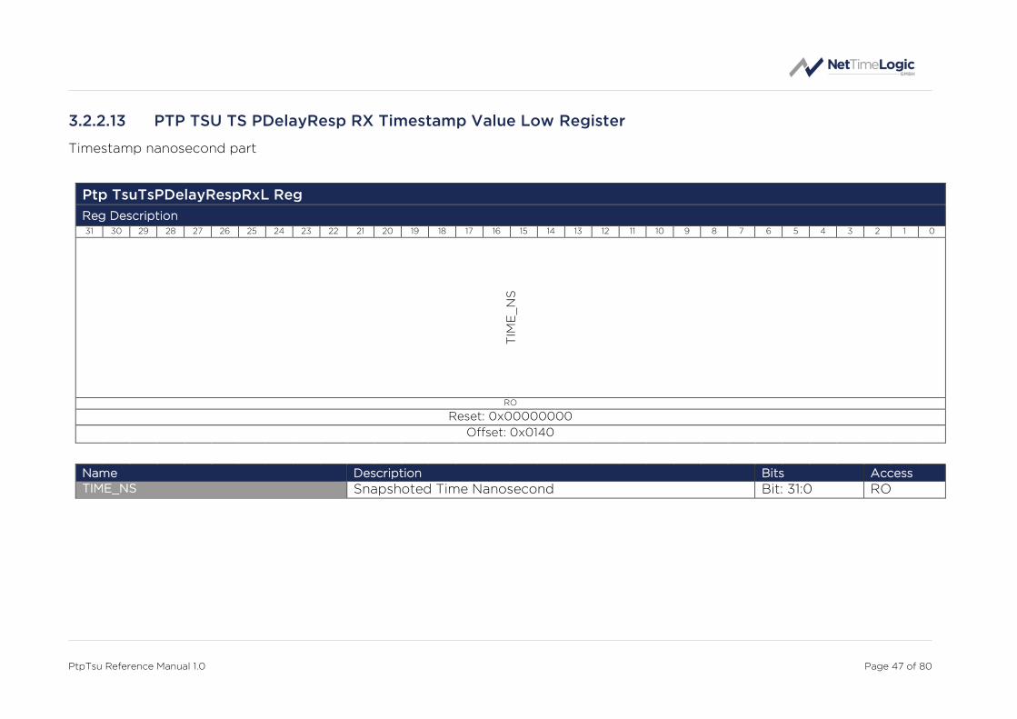
3.2.2.13 PTP TSU TS PDelayResp RX Timestamp Value Low Register
Timestamp nanosecond part
Ptp TsuTsPDelayRespRxL Reg
Reg Description
31 30 29 28 27 26 25 24 23 22 21 20 19 18 17 16 15 14 13 12 11 10 9 8 7 6 5 4 3 2 1 0
TIM
E_
NS
RO
Reset: 0x00000000
Offset: 0x0140
Name Description Bits Access
TIME_NS Snapshoted Time Nanosecond Bit: 31:0 RO

PtpTsu Reference Manual 1.0 Page 48 of 80
3.2.2.14 PTP TSU TS PDelayResp RX Timestamp Value High Register
Timestamp second part
Ptp TsuTsPDelayRespRxH Reg
Reg Description
31 30 29 28 27 26 25 24 23 22 21 20 19 18 17 16 15 14 13 12 11 10 9 8 7 6 5 4 3 2 1 0
TIM
E_
S
RO
Reset: 0x00000000
Offset: 0x0144
Name Description Bits Access
TIME_S Snapshoted Time Second Bit: 31:0 RO

PtpTsu Reference Manual 1.0 Page 49 of 80
3.2.2.15 PTP TSU TS PDelayResp TX Timestamp Value Low Register
Timestamp nanosecond part
Ptp TsuTsPDelayRespTxL Reg
Reg Description
31 30 29 28 27 26 25 24 23 22 21 20 19 18 17 16 15 14 13 12 11 10 9 8 7 6 5 4 3 2 1 0
TIM
E_
NS
RO
Reset: 0x00000000
Offset: 0x0148
Name Description Bits Access
TIME_NS Snapshoted Time Nanosecond Bit: 31:0 RO

PtpTsu Reference Manual 1.0 Page 50 of 80
3.2.2.16 PTP TSU TS PDelayResp TX Timestamp Value High Register
Timestamp second part
Ptp TsuTsPDelayRespTxH Reg
Reg Description
31 30 29 28 27 26 25 24 23 22 21 20 19 18 17 16 15 14 13 12 11 10 9 8 7 6 5 4 3 2 1 0
TIM
E_
S
RO
Reset: 0x00000000
Offset: 0x014C
Name Description Bits Access
TIME_S Snapshoted Time Second Bit: 31:0 RO

PtpTsu Reference Manual 1.0 Page 51 of 80
3.2.2.17 PTP TSU TS Sync RX Timestamp Value Low Register
Timestamp nanosecond part
Ptp TsuTsSyncRxL Reg
Reg Description
31 30 29 28 27 26 25 24 23 22 21 20 19 18 17 16 15 14 13 12 11 10 9 8 7 6 5 4 3 2 1 0
TIM
E_
NS
RO
Reset: 0x00000000
Offset: 0x0150
Name Description Bits Access
TIME_NS Snapshoted Time Nanosecond Bit: 31:0 RO

PtpTsu Reference Manual 1.0 Page 52 of 80
3.2.2.18 PTP TSU TS Sync RX Timestamp Value High Register
Timestamp second part
Ptp TsuTsSyncRxH Reg
Reg Description
31 30 29 28 27 26 25 24 23 22 21 20 19 18 17 16 15 14 13 12 11 10 9 8 7 6 5 4 3 2 1 0
TIM
E_
S
RO
Reset: 0x00000000
Offset: 0x0154
Name Description Bits Access
TIME_S Snapshoted Time Second Bit: 31:0 RO

PtpTsu Reference Manual 1.0 Page 53 of 80
3.2.2.19 PTP TSU TS Sync TX Timestamp Value Low Register
Timestamp nanosecond part
Ptp TsuTsSyncTxL Reg
Reg Description
31 30 29 28 27 26 25 24 23 22 21 20 19 18 17 16 15 14 13 12 11 10 9 8 7 6 5 4 3 2 1 0
TIM
E_
NS
RO
Reset: 0x00000000
Offset: 0x0158
Name Description Bits Access
TIME_NS Snapshoted Time Nanosecond Bit: 31:0 RO

PtpTsu Reference Manual 1.0 Page 54 of 80
3.2.2.20 PTP TSU TS Sync TX Timestamp Value High Register
Timestamp second part
Ptp TsuTsSyncTxH Reg
Reg Description
31 30 29 28 27 26 25 24 23 22 21 20 19 18 17 16 15 14 13 12 11 10 9 8 7 6 5 4 3 2 1 0
TIM
E_
S
RO
Reset: 0x00000000
Offset: 0x015C
Name Description Bits Access
TIME_S Snapshoted Time Second Bit: 31:0 RO

PtpTsu Reference Manual 1.0 Page 55 of 80
4 Design Description
The following chapters describe the internals of the PTP Timestamp Unit: starting
with the Top Level, which is a collection of subcores, followed by the description of
all subcores.
4.1 Top Level – PTP Tsu
4.1.1.1 Parameters
The core must be parametrized at synthesis time. There are a couple of parameters
which define the final behavior and resource usage of the core.
Name Type Size Description
DefaultProfileSup-
port_Gen boolean 1
If the core shall support the
PTP Default Profile
PowerProfileSup-
port_Gen boolean 1
If the core shall support the
PTP Power Profile
UtilityProfileSup-
port_Gen boolean 1
If the core shall support the
PTP Utility Profile
Layer2Support_Gen boolean 1
If in Default Profile if Layer 2
shall be supported (Power
and Utility Profile always use
Layer 2)
Layer3Support_Gen boolean 1
If in Default Profile if Layer 3
shall be supported (Power
and Utility Profile always use
Layer 2)
ClockClkPeriod
Nanosecond_Gen natural 1
Clock Period in Nanosecond:
Default for 50 MHz = 20 ns
RxDelayNanosecond
10_Gen integer 1
PHY receive delay (10Mbit)
RxDelayNanosecond
100_Gen integer 1
PHY receive delay (100Mbit)
RxDelayNanosecond
1000_Gen integer 1
PHY receive delay (1000Mbit)

PtpTsu Reference Manual 1.0 Page 56 of 80
TxDelayNanosecond
10_Gen integer 1
PHY transmit delay (10Mbit)
TxDelayNanosecond
100_Gen integer 1
PHY transmit delay (100Mbit)
TxDelayNanosecond
1000_Gen integer 1
PHY transmit delay
(1000Mbit)
AxiAddressRang
Low_Gen std_logic_vector 32
AXI Base Address
AxiAddressRange
High_Gen std_logic_vector 32
AXI Base Address plus Regis-
terset Size
Default plus 0xFFFF
Sim_Gen boolean 1
If in Testbench simulation
mode:
true = Simulation, false = Syn-
thesis
Table 5: Parameters
One of the three parameters DefaultSupport_Gen, PowerProfileSupport_Gen and
UtilityProfileSupport_Gen has to be true.
4.1.1.2 Structured Types
4.1.1.2.1 Clk_Time_Type
Defined in Clk_Package.vhd of library ClkLib
Type represents the time used everywhere. For this type overloaded operators +
and – with different parameters exist.
Field Name Type Size Description
Second std_logic_vector 32 Seconds of time
Nanosecond std_logic_vector 32 Nanoseconds of time
Fraction std_logic_vector 2 Fraction numerator (mostly
not used)
Sign std_logic 1 Positive or negative time, 1 =
negative, 0 = positive.
TimeJump std_logic 1 Marks when the clock makes a
time jump (mostly not used)
Table 6: Clk_Time_Type

PtpTsu Reference Manual 1.0 Page 57 of 80
4.1.1.2.2 Ptp_TsuInfo_Type
Defined in Ptp_Package.vhd of library PtpLib
Type represents the information which frame type was detected and the start of
frame. For this type an overloaded OR operators exist.
Field Name Type Size Description
Sync std_logic 1 Sync frame detected
DelayReq std_logic 1 DelayReq frame detected
PdelayReq std_logic 1 PdelayReq frame detected
PdelayResp std_logic 1 PdelayResp frame detected
SyncFollowUp std_logic 1 SyncFollowUp frame detected
DelayResp std_logic 1 DelayResp frame detected
PdelayRespFollowUp std_logic 1 PdelayRespFollowUp frame
detected
Announce std_logic 1 Announce frame detected
Signaling std_logic 1 Signaling frame detected
Management std_logic 1 Management frame detected
SfdDetected std_logic 1 Start of frame detected
Table 7: Ptp_TsuInfo_Type
4.1.1.3 Entity Block Diagram
TsuInfoRx
MAC ETHITF
ADAPTER
(R)(G)MII RX
PHY ETHITF
ADAPTER
(R)(G)MII TXTSU
PROC.AXIS
TSUPROC.
SFD
AXIS
SFD
REGISTERSET
AXI MM
TsuInfoTx
IRQ
LinkSpeed
TsuInfoRx
TsuInfoTx
Figure 10: PTP Tsu

PtpTsu Reference Manual 1.0 Page 58 of 80
4.1.1.4 Entity Description
Tsu Processor
This module handles all incoming frames. It does the frame parsing and passes this
information to the register set. In addition, it realigns the 32bit stream so the PTP
frames are always aligned the same way in case an IP header or HSR tag is in-
serted.
See 4.2.1 for more details.
MAC & PHY Ethernet Interface Adapter
This module converts the Media Independent Interface (MII) to AXI stream and vice
versa (unused). In parallel it has a SFD detector for each path which generates an
event when a SFD is detected; this is used for timestamping.
See 4.2.2 for more details.
Registerset
This module is an AXI Light Memory Mapped Slave. It provides access to all Da-
tasets and allows to configure the PTP Timestamp Unit. A AXI Master has to con-
figure the TSU with AXI writes to the registers, which is typically done by a CPU
See 4.2.3 for more details.
4.1.1.5 Entity Declaration
Name Dir Type Size Description
Generics
General DefaultProfile
Support_Gen - boolean 1
Support for Default
Profile
PowerProfile
Support_Gen - boolean 1
Support for Power
Profile
UtilityProfile
Support_Gen - boolean 1
Support for Utility
Profile
Layer2Support_Gen - boolean 1 Support for Layer 2
Mapping
Layer3Support_Gen - boolean 1 Support for Layer 3
Mapping
ClockClkPeriodNano-
second_Gen - natural 1
Integer Clock Period

PtpTsu Reference Manual 1.0 Page 59 of 80
RxDelayNanosecond
10_Gen - integer 1
RX Delay of the PHY
in Nanosecond
RxDelayNanosecond
100_Gen - integer 1
RX Delay of the PHY
in Nanosecond
RxDelayNanosecond
1000_Gen - integer 1
RX Delay of the PHY
in Nanosecond
TxDelayNanosecond
10_Gen - integer 1
TX Delay of the PHY
in Nanosecond
TxDelayNanosecond
100_Gen - integer 1
TX Delay of the PHY
in Nanosecond
TxDelayNanosecond
1000_Gen - integer 1
TX Delay of the PHY
in Nanosecond
AxiAddressRange
Low_Gen - std_logic_vector 32
AXI Base Address
AxiAddressRange
High_Gen - std_logic_vector 32
AXI Base Address
plus Registerset
Size
Sim_Gen - boolean 1 If in Testbench sim-
ulation mode
Ports
System SysClk_ClkIn in std_logic 1 System Clock
SysRstN_RstIn in std_logic 1 System Reset
Time Input
ClockTime_DatIn in Clk_Time_Type 1 Adjusted PTP Clock
Time
ClockTime_ValIn in std_logic 1 Adjusted PTP Clock
Time valid
Tsu Info Input (TsuExt only)
TsuInfoRx_DatIn in Ptp_TsuInfo_Type 1
Timestamp Unit in-
formation from RX
path
TsuInfoTx_DatIn in Ptp_TsuInfo_Type 1
Timestamp Unit in-
formation from TX
path
(R)(G)Mii RX Clk/Rst Input
(R)(G)MiiRxClk_ClkIn in std_logic 1 RX Clock
(R)(G)MiiRxRstN_RstIn
in std_logic 1 Reset aligned with
RX Clock

PtpTsu Reference Manual 1.0 Page 60 of 80
(R)(G)Mii TX Clk/Rst Input
(R)(G)MiiTxClk_ClkIn in std_logic 1 RX Clock
(R)(G)MiiTxRstN_RstIn
in std_logic 1 Reset aligned with
RX Clock
(R)(G)Mii RX Data Input
(R)(G)MiiRxDv_EnaIn in std_logic 1 RX Data valid
®(G)MiiRx_ErrIn in std_logic 1 RX Error
®(G)MiiRxData_DatIn in std_logic_vector 2-8
RX Data
MII:4, RMII:2, GMII:8,
RGMII:4
®(G)MiiCol_DatIn in std_logic 1 Collision
®(G)MiiCrs_DatIn in std_logic 1 Carrier Sense
®(G)Mii TX Data Input
®(G)MiiTxEn_EnaIn in std_logic 1 TX Data valid
®(G)MiiTxErr_ErrIn in std_logic 1 TX Error
®(G)MiiTxData_DatIn in std_logic_vector 2-8
TX Data
MII:4, RMII:2, GMII:8,
RGMII:4
AXI4 Light Slave AxiWriteAddrValid _ValIn
in std_logic 1 Write Address Valid
AxiWriteAddrReady _RdyOut
out std_logic 1 Write Address
Ready
AxiWriteAddrAddress _AdrIn
in std_logic_vector 32 Write Address
AxiWriteAddrProt _DatIn
in std_logic_vector 3 Write Address Pro-
tocol
AxiWriteDataValid _ValIn
in std_logic 1 Write Data Valid
AxiWriteDataReady _RdyOut
out std_logic 1 Write Data Ready
AxiWriteDataData _DatIn
in std_logic_vector 32 Write Data
AxiWriteDataStrobe _DatIn
in std_logic_vector 4 Write Data Strobe
AxiWriteRespValid _ValOut
out std_logic 1 Write Response
Valid
AxiWriteRespReady _RdyIn
in std_logic 1 Write Response
Ready
AxiWriteResp Response_DatOut
out std_logic_vector 2 Write Response
AxiReadAddrValid _ValIn
in std_logic 1 Read Address Valid

PtpTsu Reference Manual 1.0 Page 61 of 80
AxiReadAddrReady _RdyOut
out std_logic 1 Read Address
Ready
AxiReadAddrAddress _AdrIn
in std_logic_vector 32 Read Address
AxiReadAddrProt _DatIn
in std_logic_vector 3 Read Address Pro-
tocol
AxiReadDataValid _ValOut
out std_logic 1 Read Data Valid
AxiReadDataReady _RdyIn
in std_logic 1 Read Data Ready
AxiReadData Response_DatOut
out std_logic_vector 2 Read Data
AxiReadDataData _DatOut
out std_logic_vector 32 Read Data Re-
sponse
Interrupt Output Irq_EvtOut out std_logic 1 Level high Interrupt
Table 8: PTP Tsu

PtpTsu Reference Manual 1.0 Page 62 of 80
4.2 Design Parts
The PTP Timestamp Unit core consists of a couple of subcores. Each of the sub-
cores itself consist again of smaller function block. The following chapters describe
these subcores and their functionality.
4.2.1 Tsu Processor
4.2.1.1 Entity Block Diagram
RE-ALIGNER
DETECTORAXISAXIS
SFD Detect
TsuInfo
Figure 11: Tsu Processor
4.2.1.2 Entity Description
Re-Aligner
This module allows aligning the AXI Data stream as required. It is only instantiated
if Layer 3 or Utility mapping is used. The input can be 32/24/16/8 bit aligned and
the output can also be 32/24/16/8 bit aligned. From an external input, the output
alignment can be requested. This is used for alignment of the PTP start to a 32 bit
boundary (Some mappings cause that the header is not 32 bit aligned anymore)
again, and for realignment to a constant 32bit wide stream again.
Detector
This module parses all incoming Ethernet frames. It extracts the frame type in the
case of PTP frames. If Layer 3 mapping or the Utility Profile is used it request a spe-
cific alignment from the Realigner so the PTP frame is starting 32 bit aligned again.
4.2.1.3 Entity Declaration
Name Dir Type Size Description
Generics
Interface Adapter DefaultProfile
Support_Gen - boolean 1
Support for Default
Profile

PtpTsu Reference Manual 1.0 Page 63 of 80
PowerProfile
Support_Gen - boolean 1
Support for Power
Profile
UtilityProfile
Support_Gen - boolean 1
Support for Utility
Profile
Layer2Support_Gen - boolean 1 Support for Layer 2
Mapping
Layer3Support_Gen - boolean 1 Support for Layer 3
Mapping
Ports
System SysClk_ClkIn in std_logic 1 System Clock
SysRstN_RstIn in std_logic 1 System Reset
SfdDetected Input
SfdDetected_EvtOut in std_logic 1 Start of Frame De-
limiter detected
Axi Input
AxisValid_ValIn in std_logic 1 AXI Stream frame
input AxisReady_ValOut out std_logic 1
AxisData_DatIn in std_logic_vector 32
AxisStrobe_ValIn in std_logic_vector 4
AxisKeep_ValIn in std_logic_vector 4
AxisLast_ValIn in std_logic 1
AxisUser_DatIn in std_logic_vector 3
Tsu Info Output
TsuInfo_DatOut out Ptp_TsuInfo_Type 1 Timestamp and
Frame Info
Table 9: Ethernet Interface Adapter

PtpTsu Reference Manual 1.0 Page 64 of 80
4.2.2 Ethernet Interface Adapter
4.2.2.1 Entity Block Diagram
SFDDETECT
TX/RX ITFADAPTER
RX/TX ITFADAPTER
(R)(G)MII RX/TX
(R)(G)MII TX/RX
SFDDETECT
AXIS
AXIS
SFD Detect OUT
SFD Detect IN LinkSpeed
Figure 12: Ethernet Interface Adapter
4.2.2.2 Entity Description
SFD Detector
This module detects the Start of Frame Delimiter (SFD) on the (R)(G)MII stream. It
runs directly on the (R)(G)MII clock domain for minimal jitter on the timestamp
point detection. Once the SFD is detected, an event is signaled which is used by
the timestamper.
RX/TX Interface Adapter (In)
This module convert the Media Independent Interface (R)(G)MII data stream
(2/4/8bit) into a 32bit AXI stream. First bytes on the cable are mapped to the AXI
MSB of the data array. It contains an asynchronous Fifo to on one hand do clock
domain crossing from the external clock to the system clock and on the other hand
also to minimal buffer data for speed differences. The Fifo size is kept quite small
to assure correct timestamp alignment with the frame. It converts the different
data widths into a 32bit block AXI stream. The Preamble and SFD are removed on
reception. Also, it detects the link speed based on the interface clock.
TX/RX Interface Adapter (Out unused)
This module convert the 32bit AXI stream into a Media Independent Interface
(R)(G)MII data stream (2/4/8bit) which is continuous. The MSB of the AXI data ar-
ray is mapped to the first byte on the cable. It contains an asynchronous Fifo to on

PtpTsu Reference Manual 1.0 Page 65 of 80
one hand do clock domain crossing from the system clock to the external clock
and on the other hand also to minimal buffer data for speed differences. The Fifo
size is kept quite small to assure correct timestamp alignment with the frame. It
converts the 32bit block AXI stream into the different data widths. The Preamble
and SFD are added before transmission. It also assures the correct interframe gap
between frames.
4.2.2.3 Entity Declaration
Name Dir Type Size Description
Generics
Interface Adapter ClockClkPeriod
Nanosecond_Gen - natural 1
Clock Period in Na-
nosecond
IoFf_Gen - boolean 1 Shall IO flip flops be
instantiated
Ports
System SysClk_ClkIn in std_logic 1 System Clock
SysRstN_RstIn in std_logic 1 System Reset
(R)(G)Mii RX Clk/Rst Input
(R)(G)MiiRxClk_ClkIn in std_logic 1 RX Clock
(R)(G)MiiRxRstN_RstIn
in std_logic 1 Reset aligned with
RX Clock
(R)(G)Mii TX Clk/Rst Input
(R)(G)MiiTxClk_ClkIn in std_logic 1 RX Clock
(R)(G)MiiTxRstN_RstIn
in std_logic 1 Reset aligned with
RX Clock
(R)(G)Mii RX Data Input/Output
(R)(G)MiiRxDv_Ena In/
out std_logic 1
RX Data valid
(R)(G)MiiRxErr_Ena In/
out std_logic 1
RX Error
(R)(G)MiiRxData_Dat In/
out std_logic_vector 2-8
RX Data
MII:4, RMII:2, GMII:8,
RGMII:4
(R)(G)MiiCol_Dat In/
out std_logic 1
Collision

PtpTsu Reference Manual 1.0 Page 66 of 80
(R)(G)MiiCrs_Dat In/
out std_logic 1
Carrier Sense
(R)(G)Mii TX Data Input
(R)(G)MiiTxEn_Ena In/
out std_logic 1
TX Data valid
(R)(G)MiiTxErr_Ena In/
out std_logic 1
TX Error
(R)(G)MiiTxData_Dat In/
out std_logic_vector 2-8
TX Data
MII:4, RMII:2, GMII:8,
RGMII:4
SfdDetected Output
(R)(G)MiiInSfdDe-tected_EvtOut
out std_logic 1 Start of Frame De-
limiter detected
(R)(G)MiiOutSfdDe-tected_EvtOut
out std_logic 1 Start of Frame De-
limiter detected
Link Speed Output
LinkSpeed_DatOut out Common_Link-
Speed_Type 1
Link Speed ot the
interface
Axi Input
AxisValid_ValIn in std_logic 1 AXI Stream frame
input AxisReady_ValOut out std_logic 1
AxisData_DatIn in std_logic_vector 32
AxisStrobe_ValIn in std_logic_vector 4
AxisKeep_ValIn in std_logic_vector 4
AxisLast_ValIn in std_logic 1
AxisUser_DatIn in std_logic_vector 3
Axi Output
AxisValid_ValOut out std_logic 1 AXI Stream frame
output AxisReady_ValIn in std_logic 1
AxisData_DatOut out std_logic_vector 32
AxisStrobe_ValOut out std_logic_vector 4
AxisKeep_ValOut out std_logic_vector 4
AxisLast_ValOut out std_logic 1
AxisUser_DatOut out std_logic_vector 3
Table 10: Ethernet Interface Adapter

PtpTsu Reference Manual 1.0 Page 67 of 80
4.2.3 Registerset
4.2.3.1 Entity Block Diagram
TsuInfoRx
REGISTERSET
Irq
AXI MM TsuInfoTx
RXTS
TXTS
TxTs
RxTs
Time
LinkSpeed
Figure 13: Registerset
4.2.3.2 Entity Description
Register Set
This module is an AXI Light Memory Mapped Slave. It provides access to all
Timestamps and allows configuring the PTP Timestamp Unit. AXI4 Light only sup-
ports 32 bit wide data access, no byte enables, no burst, no simultaneous read and
writes and no unaligned access. To change configuration this shall be done via AXI
writes to the registers, which is typically done by a CPU. Parameters can in this
case be changed at runtime.
In addition to AXI access it also handles the whole interrupt and snapshot logic for
the different frame types and directions. It takes the timestamps from the
timestampers together with the TsuInfo to figure out for which frame type and di-
rection a new snapshot has to be done.
The snapshot logic makes sure that timestamps are always consistent and get not
overwitten if not cleared and detects if a timestamp was missed because of a not
cleared timestamp.
RX Timestamper
This module takes a snapshot of the Adjusted Clock when the SFD detected event
was asserted by the Interface Adapter. It also compensates the PHY delay depend-
ing on the link speed.

PtpTsu Reference Manual 1.0 Page 68 of 80
TX Timestamper
This module takes a snapshot of the Adjusted Clock when the SFD detected event
was asserted by the Interface Adapter. It also compensates the PHY delay depend-
ing on the link speed.
4.2.3.3 Entity Declaration
Name Dir Type Size Description
Generics
General ClockClkPeriodNano-
second_Gen - natural 1
Integer Clock Period
RxDelayNanosecond
10_Gen - integer 1
RX Delay of the PHY
in Nanosecond
RxDelayNanosecond
100_Gen - integer 1
RX Delay of the PHY
in Nanosecond
RxDelayNanosecond
1000_Gen - integer 1
RX Delay of the PHY
in Nanosecond
TxDelayNanosecond
10_Gen - integer 1
TX Delay of the PHY
in Nanosecond
TxDelayNanosecond
100_Gen - integer 1
TX Delay of the PHY
in Nanosecond
TxDelayNanosecond
1000_Gen - integer 1
TX Delay of the PHY
in Nanosecond
AxiAddressRange
Low_Gen - std_logic_vector 32
AXI Base Address
AxiAddressRange
High_Gen - std_logic_vector 32
AXI Base Address
plus Registerset
Size
Register Set
StaticConfig_Gen - boolean 1 If Static Configura-
tion or AXI is used
AxiAddressRange
Low_Gen - std_logic_vector 32
AXI Base Address
AxiAddressRange
High_Gen - std_logic_vector 32
AXI Base Address
plus Registerset
Size
Ports

PtpTsu Reference Manual 1.0 Page 69 of 80
System SysClk_ClkIn in std_logic 1 System Clock
SysRstN_RstIn in std_logic 1 System Reset
Time Input
ClockTime_DatIn in Clk_Time_Type 1 Adjusted PTP Clock
Time
ClockTime_ValIn in std_logic 1 Adjusted PTP Clock
Time valid
AXI4 Light Slave AxiWriteAddrValid _ValIn
in std_logic 1 Write Address Valid
AxiWriteAddrReady _RdyOut
out std_logic 1 Write Address
Ready
AxiWriteAddrAddress _AdrIn
in std_logic_vector 32 Write Address
AxiWriteAddrProt _DatIn
in std_logic_vector 3 Write Address Pro-
tocol
AxiWriteDataValid _ValIn
in std_logic 1 Write Data Valid
AxiWriteDataReady _RdyOut
out std_logic 1 Write Data Ready
AxiWriteDataData _DatIn
in std_logic_vector 32 Write Data
AxiWriteDataStrobe _DatIn
in std_logic_vector 4 Write Data Strobe
AxiWriteRespValid _ValOut
out std_logic 1 Write Response
Valid
AxiWriteRespReady _RdyIn
in std_logic 1 Write Response
Ready
AxiWriteResp Response_DatOut
out std_logic_vector 2 Write Response
AxiReadAddrValid _ValIn
in std_logic 1 Read Address Valid
AxiReadAddrReady _RdyOut
out std_logic 1 Read Address
Ready
AxiReadAddrAddress _AdrIn
in std_logic_vector 32 Read Address
AxiReadAddrProt _DatIn
in std_logic_vector 3 Read Address Pro-
tocol
AxiReadDataValid _ValOut
out std_logic 1 Read Data Valid
AxiReadDataReady _RdyIn
in std_logic 1 Read Data Ready
AxiReadData Response_DatOut
out std_logic_vector 2 Read Data

PtpTsu Reference Manual 1.0 Page 70 of 80
AxiReadDataData _DatOut
out std_logic_vector 32 Read Data Re-
sponse
Link Speed Input
LinkSpeed_DatIn in Common_Link-
Speed_Type 1
Link Speed ot the
interface
Tsu Info Input
TsuInfoRx_DatIn in Ptp_TsuInfo_Type 1
Timestamp Unit in-
formation from RX
path
TsuInfoTx_DatIn in Ptp_TsuInfo_Type 1
Timestamp Unit in-
formation from TX
path
Interrupt Output
Irq_EvtOut out std_logic 1 Level High interrupt
output
Table 11: Registerset
PtpTsu Reference Manual 1.0 Page 71 of 80
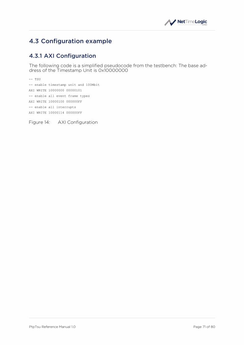
4.3 Configuration example
4.3.1 AXI Configuration
The following code is a simplified pseudocode from the testbench: The base ad-dress of the Timestamp Unit is 0x10000000 -- TSU
-- enable timestamp unit and 100Mbit
AXI WRITE 10000000 00000101
-- enable all event frame types
AXI WRITE 10000100 000000FF
-- enable all interrupts
AXI WRITE 10000114 000000FF
Figure 14: AXI Configuration

PtpTsu Reference Manual 1.0 Page 72 of 80
4.4 Clocking and Reset Concept
4.4.1 Clocking
To keep the design as robust and simple as possible, the whole Timestamp Unit, in-
cluding the Counter Clock and all other cores from NetTimeLogic are run in one
clock domain. This is considered to be the system clock. Per Default this clock is
50MHz. Where possible also the interfaces are run synchronous to this clock. For
clock domain crossing asynchronous Fifos with gray counters or message patterns
with meta-stability flip-flops are used. Clock domain crossings for the AXI interface
is moved from the AXI slave to the AXI interconnect.
Clock Frequency Description
System
System Clock 50MHz
(Default)
System clock where the OC runs on as
well as the counter clock etc.
(R)(G)MII Interfaces
PHY (R)(G)MII RX
Clocks 2.5/25/125MHz
Asynchronous, external receive clocks
from the PHYs also used for the MAC.
Depending on the interface not all fre-
quencies apply.
PHY (R)(G)MII TX
Clocks 2.5/25/125MHz
Asynchronous, external transmit clocks
to/from the PHYs also used for the MAC.
Depending on the interface not all fre-
quencies apply.
AXI Interface
AXI Clock 50MHz
(Default)
Internal AXI bus clock, same as the sys-
tem clock
Table 12: Clocks
4.4.2 Reset
In connection with the clocks, there is a reset signal for each clock domain. All re-
sets are active low. All resets can be asynchronously set and shall be synchronously
released with the corresponding clock domain. All resets shall be asserted for the
first couple (around 8) clock cycles. All resets shall be set simultaneously and re-
leased simultaneously to avoid overflow conditions in the core. See the reference
designs top file for an example of how the reset shall be handled.

PtpTsu Reference Manual 1.0 Page 73 of 80
Reset Polarity Description
System
System Reset Active low Asynchronous set, synchronous release
with the system clock
(R)(G)MII Interface PHY (R)(G)MII RX Re-
set Active low
Asynchronous set, synchronous release
with the (R)(G)MII RX clock
PHY (R)(G)MII TX Re-
set Active low
Asynchronous set, synchronous release
with the (R)(G)MII TX clock
AXI Interface
AXI Reset Active low
Asynchronous set, synchronous release
with the AXI clock, which is the same as
the system clock
Table 13: Resets

PtpTsu Reference Manual 1.0 Page 74 of 80
5 Resource Usage
Since the FPGA Architecture between vendors and FPGA families differ there is a
split up into the two major FPGA vendors.
5.1 Altera (Cyclone V)
Configuration FFs LUTs BRAMs DSPs
Minimal (Only Default Profile, L2) 1163 1838 4 0
Maximal (All Profiles, L2 & L3) 1485 2739 4 0
Table 14: Resource Usage Altera
5.2 Xilinx (Artix 7)
Configuration FFs LUTs BRAMs DSPs
Minimal (Only Default Profile, L2) 1237 1615 4 0
Maximal (All Profiles, L2 & L3) 1539 2523 4 0
Table 15: Resource Usage Xilinx

PtpTsu Reference Manual 1.0 Page 75 of 80
6 Delivery Structure
AXI -- AXI library folder
|-Library -- AXI library component sources
|-Package -- AXI library package sources
CLK -- CLK library folder
|-Library -- CLK library component sources
|-Package -- CLK library package sources
COMMON -- COMMON library folder
|-Library -- COMMON library component sources
|-Package -- COMMON library package sources
PPS -- PPS library folder
|-Package -- PPS library package sources
PTP -- PTP library folder
|-Core -- PTP library cores
|-Doc -- PTP library cores documentations
|-Driver -- PTP library driver
|-Library -- PTP library component sources
|-Package -- PTP library package sources
|-Refdesign -- PTP library cores reference designs
|-Software -- PTP software stack (PTP4l)
|-Testbench -- PTP library cores testbench sources and sim/log
RED -- RED library folder
|-Package -- RED library package sources
SIM -- SIM library folder
|-Doc -- SIM library command documentation
|-Package -- SIM library package sources
|-Testbench -- SIM library testbench template sources
|-Tools -- SIM simulation tools
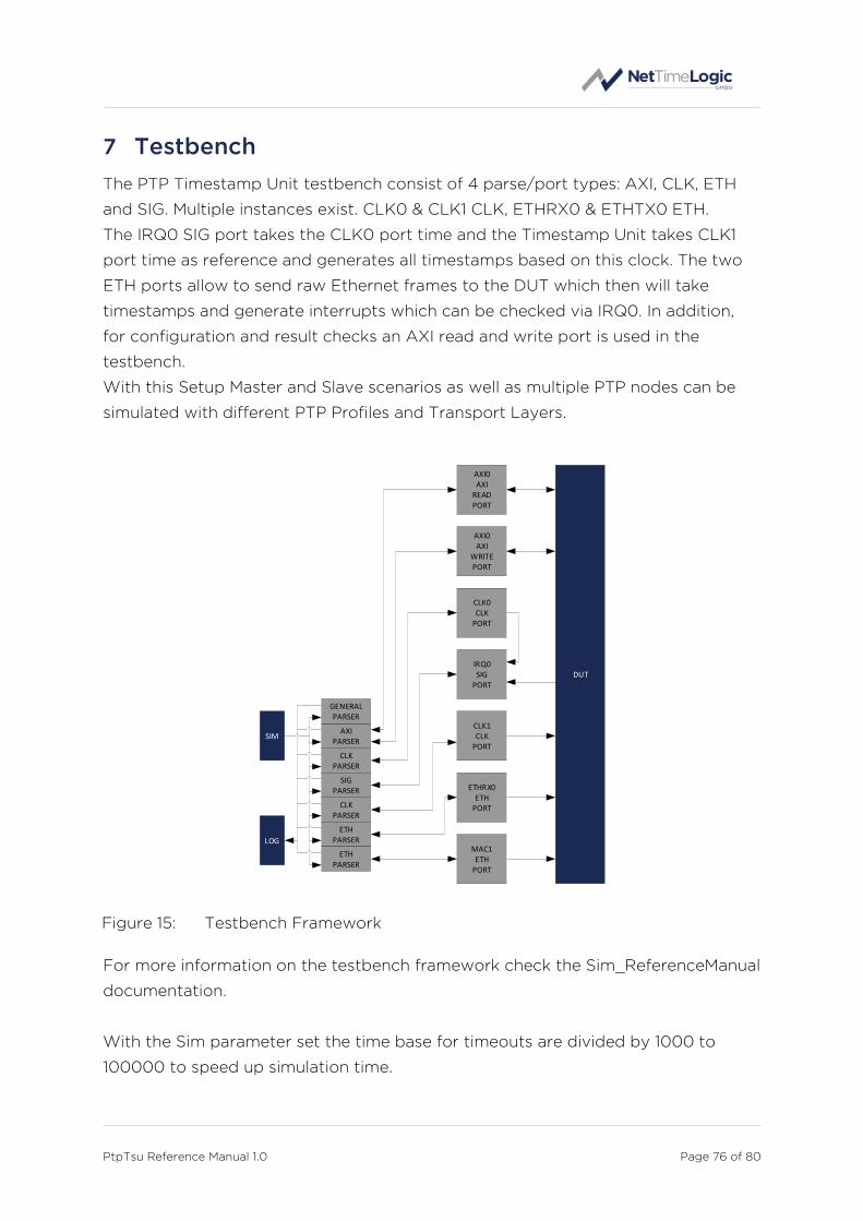
PtpTsu Reference Manual 1.0 Page 76 of 80
7 Testbench
The PTP Timestamp Unit testbench consist of 4 parse/port types: AXI, CLK, ETH
and SIG. Multiple instances exist. CLK0 & CLK1 CLK, ETHRX0 & ETHTX0 ETH.
The IRQ0 SIG port takes the CLK0 port time and the Timestamp Unit takes CLK1
port time as reference and generates all timestamps based on this clock. The two
ETH ports allow to send raw Ethernet frames to the DUT which then will take
timestamps and generate interrupts which can be checked via IRQ0. In addition,
for configuration and result checks an AXI read and write port is used in the
testbench.
With this Setup Master and Slave scenarios as well as multiple PTP nodes can be
simulated with different PTP Profiles and Transport Layers.
CLKPARSER
AXIPARSER
CLKPARSER
ETHPARSER
CLK0CLK
PORT
DUT
CLK1CLK
PORT
ETHRX0ETH
PORT
SIM
LOG
GENERALPARSER
SIGPARSER
IRQ0SIG
PORT
ETHPARSER
MAC1ETH
PORT
AXI0AXI
READPORT
AXI0AXI
WRITEPORT
Figure 15: Testbench Framework
For more information on the testbench framework check the Sim_ReferenceManual
documentation.
With the Sim parameter set the time base for timeouts are divided by 1000 to
100000 to speed up simulation time.

PtpTsu Reference Manual 1.0 Page 77 of 80
7.1 Run Testbench
1. Run the general script first
source XXX/SIM/Tools/source_with_args.tcl
2. Start the testbench with all test cases
src XXX/PTP/Testbench/Core/PtpTsu/Script/run_Ptp_TsuMii_Tb.tcl
3. Check the log files LogFileX.txt in the XXX/PTP/Testbench/Core/PtpTsu/Log/
folder for simulation results.
8 Reference Designs
The PTP Timestamp Unit reference design contains a PLL to generate all necessary
clocks (cores are run at 50 MHz), an instance of the PTP Timestamp Unit IP core,
an instance of the Adjustable Counter Clock IP core (needs to be purchased sepa-
rately) and a Zynq CPU Blockdesign. The Reference Design is intended to be con-
nected to any PTP Master or Slave device which can run in Layer 2 or Layer 3, P2P
or E2E mode in Default Profile.
The Reference Design is using 100/1000Mbit full duplex as Ethernet link. The refer-
ence design uses the Ethernet MAC (GEM0) of the hard processing system in the
Zynq device since this is where the PHY is connected to and exposes the TS signals
of the MAC to the Timestamp Unit (TsuExt).
PetaLinux 2016.2 is used as Linux distribution (but the same applies to newer ver-
sions of PetaLinux) and the necessary drivers for the MAC, the TSU and the Adjust-
able Counter clock are provided and PTP4l (http://linuxptp.sourceforge.net) is
used as PTP software stack.
All generics can be adapted to the specific needs.

PtpTsu Reference Manual 1.0 Page 78 of 80
PTPTSU
CLOCKAdjustable Clock
AXI4 Lite Slave
Time
PtpRefDesign
AXI4 Lite Slave
PLLPPSPPSMaster
AXI4 Lite Slave
ZynqCPU
System
AXI4 Master
ntl_tsuLinux Driver
ntl_phcLinux Driver
ntl_macbLinux Driver
PTP TS
PTP4lLinux PTP Software Stack
Ethernet
Figure 16: Reference Design
8.1 Xilinx: Digilent Arty Z7
The Arty Z7 board is an FPGA board from Digilent Inc. with a Zynq 7020 SoC from
Xilinx. (http://store.digilentinc.com/arty-z7-apsoc-zynq-7000-development-board-
for-makers-and-hobbyists/)
1. Open Vivado 2016.2
2. Run TCL script /PTP/Refdesign/Xilinx/ArtyZ7/PtpAllInOneClock/PtpAllI-
nOneClock.tcl
a. This has to be run only the first time and will create a new Vivado Pro-
ject
3. If the project has been created before open the project and do not rerun the
project TCL
4. If a newer version of Vivado is used update the IP cores in the block design
5. If the optional core PPS Master Clock is available add the files from the cor-
responding folders (PPS/Core, PPS/Library and PPS/Package) to the corre-
sponding Library (PpsLib).
6. Change the generics (PpsMasterAvailable_Gen) in Vivado (in the settings
menu, not in VHDL) to true for the optional cores that are available.
7. Rerun implementation
8. Export the hardware and bitstream and import them into PetaLinux 2016.2
9. Integrate the Drivers according to the Readme.txt files
10. Build PetaLinux

PtpTsu Reference Manual 1.0 Page 79 of 80
11. Create BOOT.BIN
12. Load PetaLinux BOOT.BIN and image.ub on a SdCard
13. Set bootmode on Arty Z7 to SdCard
14. Boot Arty Z7
15. Start PTP4l: ptp4l -f /etc/ptp4l.cfg
16. Adapt ptp4l.cfg as required
Figure 17: Arty Z7 (source Digilent Inc)
Alive-LED
Ethernet Port
Soft Reset
PPS LED
PPS output
Boot Config

PtpTsu Reference Manual 1.0 Page 80 of 80
A List of tables
Table 1: Revision History ......................................................................................................................4
Table 2: Definitions .................................................................................................................................. 7
Table 3: Abbreviations .......................................................................................................................... 8
Table 4: Register Set Overview ..................................................................................................... 26
Table 5: Parameters ............................................................................................................................. 56
Table 6: Clk_Time_Type .................................................................................................................... 56
Table 7: Ptp_TsuInfo_Type .............................................................................................................. 57
Table 8: PTP Tsu ..................................................................................................................................... 61
Table 9: Ethernet Interface Adapter............................................................................................ 63
Table 10: Ethernet Interface Adapter............................................................................................ 66
Table 11: Registerset ............................................................................................................................. 70
Table 12: Clocks ....................................................................................................................................... 72
Table 13: Resets ....................................................................................................................................... 73
Table 14: Resource Usage Altera .................................................................................................... 74
Table 15: Resource Usage Xilinx ...................................................................................................... 74
B List of figures
Figure 1: Context Block Diagram .................................................................................................... 10
Figure 2: Architecture Block Diagram .............................................................................................11
Figure 3: Simple setup ........................................................................................................................... 13
Figure 4: Message exchange simple setup ................................................................................. 15
Figure 5: PTP network with Boundary Clock ............................................................................. 17
Figure 6: PTP network with Transparent Clock ........................................................................ 18
Figure 7: E2E Delay measurement with BC and TC .............................................................. 20
Figure 8: P2P Delay measurement with BC and TC ............................................................... 21
Figure 9: Timestamp Incauracy in the different Layers ....................................................... 24
Figure 10: PTP Tsu ............................................................................................................................... 57
Figure 11: Tsu Processor ....................................................................................................................... 62
Figure 12: Ethernet Interface Adapter ....................................................................................... 64
Figure 13: Registerset ........................................................................................................................ 67
Figure 14: AXI Configuration ........................................................................................................... 71
Figure 15: Testbench Framework ................................................................................................ 76
Figure 16: Reference Design ........................................................................................................... 78
Figure 17: Arty Z7 (source Digilent Inc) ................................................................................... 79