PSI - 11 Feb. 20041 The Trigger System of the MEG Experiment Marco Grassi INFN - Pisa On behalf of...
17
PSI - 11 Feb. 2004 1 The Trigger System of the MEG Experiment Marco Grassi INFN - Pisa On behalf of D. Nicolò F. Morsani S. Galeotti
-
Upload
shon-blake -
Category
Documents
-
view
215 -
download
0
Transcript of PSI - 11 Feb. 20041 The Trigger System of the MEG Experiment Marco Grassi INFN - Pisa On behalf of...
PSI - 11 Feb. 2004 1
The Trigger System of the MEG Experiment
Marco Grassi
INFN - Pisa
On behalf of
D. NicolòF. Morsani S. Galeotti
PSI - 11 Feb. 2004 2
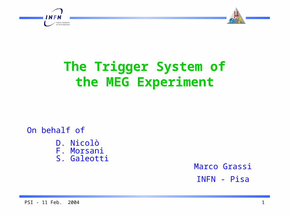
Expected Trigger RateAccidental background and
Rejection obtained by applying cuts on the following variables
• photon energy
• photon direction
• hit on the positron counter • time correlation
• positron-photon direction match
4γ 102~ 97% MeV 45 fE
99%)5.3( 1.2 oo
1-s 20 4
ff
TRfRR
e1.0
4
10 18
sR
16105 sRe
100% 102 nsT5 ; 2 ff
The rate depends on R Re+ R2
ee
e e

PSI - 11 Feb. 2004 3
The trigger implementation
Digital approach – Flash analog-to-digital converters (FADC)– Field programmable gate array (FPGA)
Final system Only 2 different board types Arranged in a tree structure on 3
layers Connected with fast LVDS buses Remote configuration/debugging
capability
Prototype boardCheck of: the FADC-FPGA compatibility chosen algorithms synchronous operation data transmission
PSI - 11 Feb. 2004 4
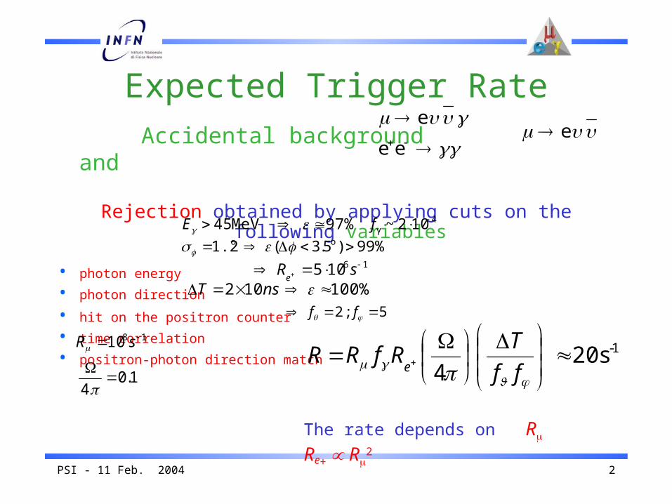
Prototype board : Type 0•VME 6U•A-to-D Conversion•Trigger•I/O
– 16 PMT signals– 2 LVDS transmitters– 4 in/2 out control signals
•Complete system test
2 boards16
16
4
Type0
Type0
TriggerStart
4
LVDS Rec
SyncTriggerStart
FADC FPGA
ControlCPLD
PMT16
16 x 10
4
48
48
VME
SyncClockSyncTriggerStart
4
48
LVDS Trans
3Out
Analog receivers
Spare in/out
Board Type0
PSI - 11 Feb. 2004 5
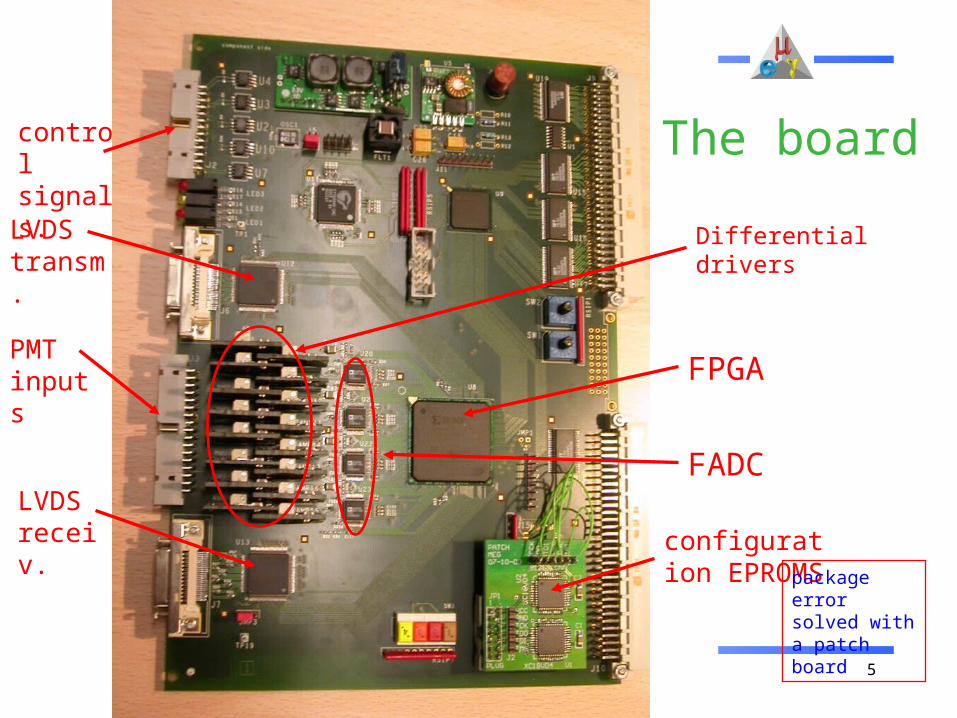
The board
PMT inputs
LVDS transm.
LVDS receiv.
FADC
FPGA
configuration EPROMS
Differential drivers
package error solved with a patch board
control signals.
PSI - 11 Feb. 2004 6
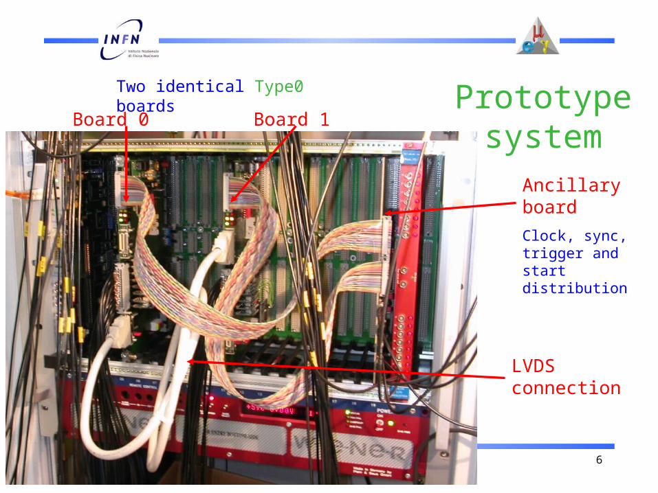
Prototype system
Board 0 Board 1
Ancillary board
Clock, sync, trigger and start distribution
LVDS connection
Two identical Type0 boards

PSI - 11 Feb. 2004 7
Prototype system
configuration
Diff. driver Fadc Proc.
Algor.
LVDS Rx
LVDS Tx
Proc. Algor.
Circ.buff
Circ.buff
Circ.buff
Circ.buff
Diff. driver Fadc Proc.
Algor.
LVDS Rx
LVDS Tx
Proc. Algor.
Circ.buff
Circ.buff
Circ.buff
Circ.buff
16 PMT
16 PMT
input
input
output
output
LVDS in
final
Board 1
Board 0
PSI - 11 Feb. 2004 8
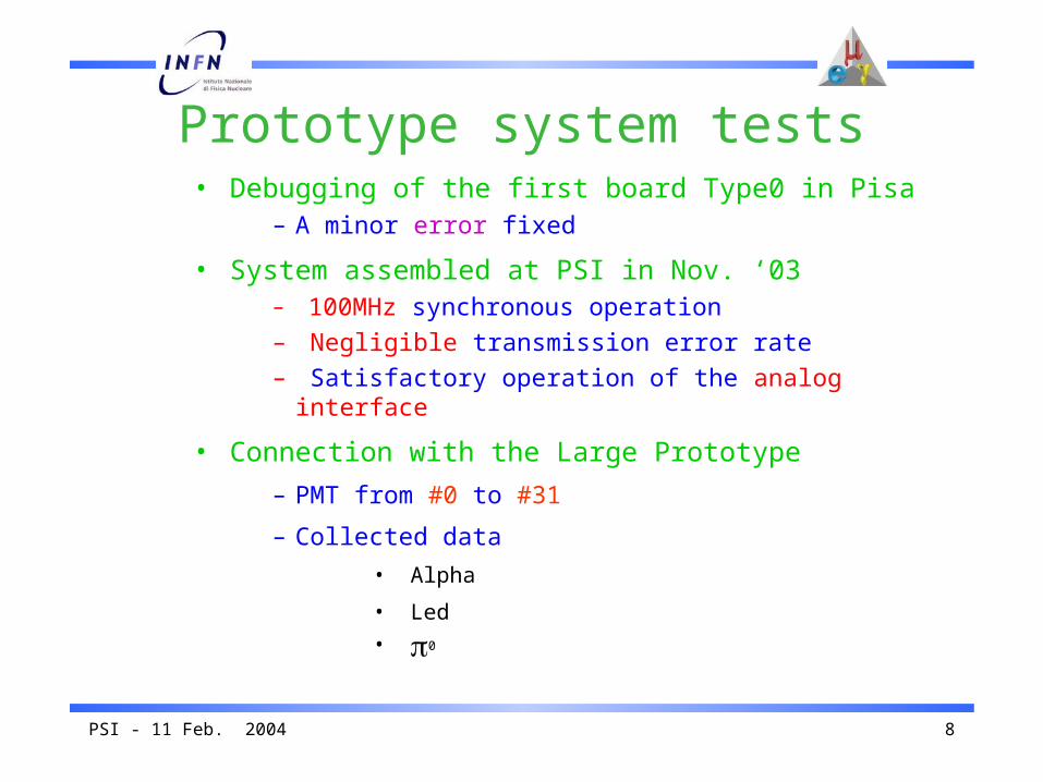
Prototype system tests• Debugging of the first board Type0 in Pisa
– A minor error fixed
• System assembled at PSI in Nov. ‘03– 100MHz synchronous operation– Negligible transmission error rate– Satisfactory operation of the analog interface
• Connection with the Large Prototype
– PMT from #0 to #31
– Collected data
• Alpha
• Led• 0

PSI - 11 Feb. 2004 9
Alpha
Time [10 ns]
Am
plit
ud
e
[mV
]
Inpu
t cy
clic-b
uffer
boar
d 1
PSI - 11 Feb. 2004 10
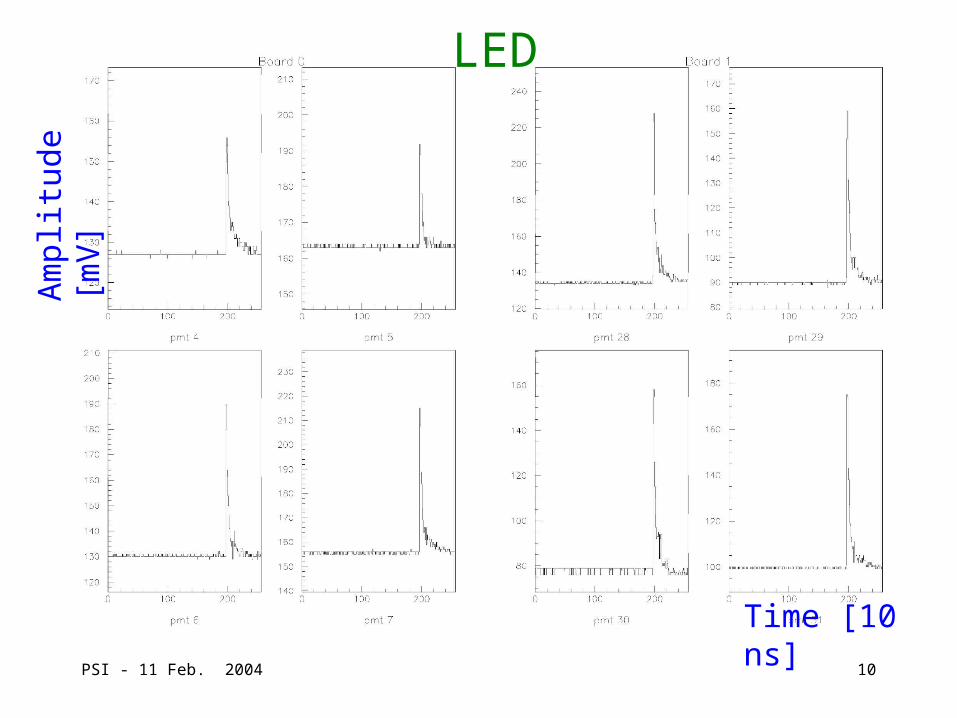
LED
Time [10 ns]
Am
plit
ud
e
[mV
]

PSI - 11 Feb. 2004 11
0
Time [10 ns]
Am
plit
ud
e
[mV
]

PSI - 11 Feb. 2004 12
Internal trigger
Time [10 ns]
Am
plit
ud
e
[mV
]
Max. Amplitude (2)
Index of Max
Amplitude sum
Pulse time
Inpu
t cy
clic-b
uffer
boar
d 0
Out
put cy
clic-
buffer
boa
rd 0

PSI - 11 Feb. 2004 13
LVDS transmission
Time [10 ns]
Am
plit
ud
e
[mV
]
Max. Amplitude (2)
Index of Max
Amplitude sum
Pulse time
Out
put cy
clic-
buffer
boa
rd 1
LVDS
inpu
t cy
clic-
buffer
boa
rd 0
7 clock cycles delay

PSI - 11 Feb. 2004 14
• 0 data• Charge spectrum• Only 32 PMT
Example of data comparison

PSI - 11 Feb. 2004 15
Further works• Hardware
– JTAG programming/debugging through VME by modifying the Type0
– Block transfer in A32D16 format (VME library to be modified)– Final characterization on linearity, cross talk …
• Analysis – Alpha, Led and 0 data to extensively check the algorithms
ConclusionsThe prototype system met all requirementsIt is available to trigger the LP in future beam tests

PSI - 11 Feb. 2004 16
Final system• Trigger location: platform
– Spy buffers to check the data flow are implemented – JTAG programming/debugging through VME: test planned with Type0
• Final boards – VirtexII or Spartan3 ?
• Main FPGA XCV812E-8-FG900 is old, first production in 2000
– Connectors• Analog input by 3M coaxial connectors• LVDS connection by 3M cables
– Differential driver on the trigger board Type1– Other components are fixed: FADC, LVDS Tx and Rx, Clock distributor– Ancillary boards: distribution of control signals
• Design of final prototypes (Type1 and Type2) june 2004– If tests are ok start of the mass production– Estimated production and test 1 year
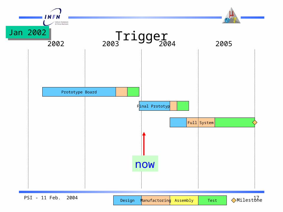
PSI - 11 Feb. 2004 17
Full System
2002 2003 2004 2005
Test MilestoneAssemblyDesign Manufactoring
Prototype Board
Final Prototype
Jan 2002Jan 2002 Trigger
now