Protecting Diodes, Transistors, and Thyristors
18
BWW CHAPTER 9 Protecting Diodes, Transistors, and Thyristors All power switching devices attain better switching performance if some form of switching aid circuit, called snubber, is employed. Snubber activation may be either passive or active which involves extra power switches. Only passive snubbers, which are based on passive electrical components, are considered in this chapter, while active snubbers are considered in Chapter 10. Fundamentally, the MOSFET and IGBT do not require switching aid circuits, but circuit imperfections, such as stray inductance and diode recovery, can necessitate the need for some form of switch snubber protection. Protection in the form of switching aid circuits performs three main functions: Divert switching losses from the switch thereby allowing a lower operating temperature, or higher electrical operating conditions for a given junction temperature. Prevent transient electrical stressing that may exceed I-V ratings thereby causing device failure. Reduce conducted and radiated electromagnetic interference Every semiconductor switching device can benefit from switching protection circuits, but extra circuit component costs and physical constraints may dictate otherwise. The bipolar diode suffers from reverse recovery current and voltage snap which induces high but short duration circuit voltages. These voltage transients may cause interference to the associated circuit and to nearby equipment. A simple series non-polarised R-C circuit connected in parallel to the stressed or offending device is often used to help suppress the voltage oscillation at diode turn-off. Such a suppression circuit can be effectively used on simple mains rectifying circuits when rectification causes conducted and radiated interference. Although the MOSFET and IGBT can usually be reliably and safely operated without external protection circuitry, stringent EMC application emission restrictions may dictate the use of snubbers. In specific applications, the IGBT is extensively current derated as its operating frequency increases. In order to attain better device current utilization, at higher frequencies, various forms of switching aid circuits can be used to divert switching losses from the stressed semiconductor switch. Generally, all thyristor devices benefit from a polarised turn-on switching aid circuit, which is based on a series connected inductor that is active at thyristor turn-on. Such an inductive turn-on snubber is obligatory for the high-power GCT and GTO thyristor. In order to fully utilise the GTO thyristor, it is usually used in conjunction with a parallel-connected capacitive turn-off snubber, which decreases device stressing during the turn-off transient. Triacs and rectifier grade SCRs and diodes tend to use a simple R-C snubber connected in parallel to the switch to reduce interference. The design procedure of the R- C snubber for a diode is different to that for the R-C snubber design for a thyristor device, because the protection objectives and initial conditions are different. In the case of a thyristor or rectifier diode, the objective is to control both the voltage rise at turn-off and recovery overshoot effects. For the fast recovery diode or any high-speed switch, the principal objectives are to control the voltage overshoot magnitude at diode snap recovery or at turn-off respectively, which are both exacerbated because of stray circuit inductance carrying current. Chapter 9 Protecting Diodes, Transistors, and Thyristors 294 L O A D s t r a y s n u b b e r 9.1 The non-polarised R-C snubber The series R-C snubber is the simplest switching aid circuit and is connected in parallel to the device being aided. It is characterized by having low series inductance and a high transient current rating. These requirements necessitate carbon type resistors for low inductance, below a few watts, and metal film resistors at higher powers. The high current and low inductance requirements are also provided by using metallised, polypropylene capacitors with high dv/dt ratings of typically hundreds of V/μs. Theoretically a purely capacitive snubber would achieve the required protection objectives, but series resistance is added to decrease the current magnitude when the capacitor is discharging and to damp any voltage oscillation by dissipating the oscillatory energy generated at turn-off when an over-voltage tends to occur. Figure 9.1. MOSFET drain to source R-C snubber protection: (a) MOSFET circuit showing stray inductance, L s , and R-C protection circuit and (b) R-C snubber optimal design curves. 9.1.1 R-C switching aid circuit for the GCT, the MOSFET, and the diode In figure 9.1a, at switch turn-off, stray inductance L s unclamped by the load freewheel diode, D f , produces an over voltage ˆ V on the MOSFET or IGBT. The energy associated with the inductor can be absorbed in the shown drain to source connected R-C circuit, thereby containing the voltage overshoot to a controlled safe level. Such an R-C snubber circuit is used extensively in thyristor circuits, 9.1.2, for dv/dt protection, but in such cases the initial current in the stray inductance is assumed zero. Here the initial inductor current is equal to the maximum load current magnitude, I ℓ . The design curves in figure 9.1b allow selection of R and C values based on the maximum voltage overshoot ˆ V and an initial current factor , defined in figure 9.1b. The C and R values are given by 2 ( / ) (F) s s I C L V (9.1) 2 / ( ) s R V I (9.2) If the R-C circuit time constant, τ = RC, is significantly less than the MOSFET voltage rise and fall times, t rv and t fv , at reset (when the capacitor is discharged through the resistor and switch at turned on), a portion of the capacitor energy 2 ½ s CV , is dissipated in the switch, as well as in R. The switch appears as a variable resistor in series with the R-C snubber. Under these conditions (t fv and t rv > RC) the resistor power loss is approximately by 0 0 0 2 2 0 0 ( ) (W) ½ ½ R R on R off C C L fv rv C s s L s s P P P P P P t t P CV f P LIf where and (9.3) otherwise (t fv and t rv < RC) the resistor losses are the energy to charge and discharge the snubber capacitor, plus the energy stored in the stray inductance, that is 2P C0 + P L0 . Note the total losses are independent of snubber resistance. The snubber resistor determines the time over which the energy is dissipated, not the amount of energy dissipated. When the R-C snubber is employed across a fast recovery diode, the peak reverse recovery current is used for I ℓ in the design procedure.
Transcript of Protecting Diodes, Transistors, and Thyristors
BWW
CHAPTER 9
Protecting Diodes, Transistors, and Thyristors
All power switching devices attain better switching performance if some form of switching aid circuit,
called snubber, is employed. Snubber activation may be either passive or active which involves extra
power switches. Only passive snubbers, which are based on passive electrical components, are
considered in this chapter, while active snubbers are considered in Chapter 10. Fundamentally, the
MOSFET and IGBT do not require switching aid circuits, but circuit imperfections, such as stray
inductance and diode recovery, can necessitate the need for some form of switch snubber protection.
Protection in the form of switching aid circuits performs three main functions:
Divert switching losses from the switch thereby allowing a lower operating temperature, or
higher electrical operating conditions for a given junction temperature.
Prevent transient electrical stressing that may exceed I-V ratings thereby causing device failure.
Reduce conducted and radiated electromagnetic interference
Every semiconductor switching device can benefit from switching protection circuits, but extra circuit
component costs and physical constraints may dictate otherwise.
The bipolar diode suffers from reverse recovery current and voltage snap which induces high but short
duration circuit voltages. These voltage transients may cause interference to the associated circuit and
to nearby equipment. A simple series non-polarised R-C circuit connected in parallel to the stressed or
offending device is often used to help suppress the voltage oscillation at diode turn-off. Such a
suppression circuit can be effectively used on simple mains rectifying circuits when rectification causes
conducted and radiated interference.
Although the MOSFET and IGBT can usually be reliably and safely operated without external protection
circuitry, stringent EMC application emission restrictions may dictate the use of snubbers. In specific
applications, the IGBT is extensively current derated as its operating frequency increases. In order to
attain better device current utilization, at higher frequencies, various forms of switching aid circuits can
be used to divert switching losses from the stressed semiconductor switch.
Generally, all thyristor devices benefit from a polarised turn-on switching aid circuit, which is based on a
series connected inductor that is active at thyristor turn-on. Such an inductive turn-on snubber is
obligatory for the high-power GCT and GTO thyristor. In order to fully utilise the GTO thyristor, it is usually
used in conjunction with a parallel-connected capacitive turn-off snubber, which decreases device
stressing during the turn-off transient. Triacs and rectifier grade SCRs and diodes tend to use a simple
R-C snubber connected in parallel to the switch to reduce interference. The design procedure of the R-
C snubber for a diode is different to that for the R-C snubber design for a thyristor device, because the
protection objectives and initial conditions are different. In the case of a thyristor or rectifier diode, the
objective is to control both the voltage rise at turn-off and recovery overshoot effects. For the fast
recovery diode or any high-speed switch, the principal objectives are to control the voltage overshoot
magnitude at diode snap recovery or at turn-off respectively, which are both exacerbated because of
stray circuit inductance carrying current.
Chapter 9 Protecting Diodes, Transistors, and Thyristors 294
LOAD
stra
y snubber
9.1 The non-polarised R-C snubber
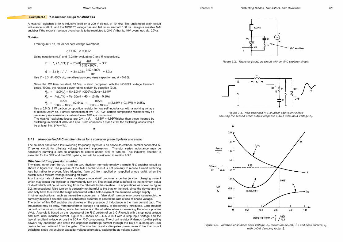
The series R-C snubber is the simplest switching aid circuit and is connected in parallel to the device being aided. It is characterized by having low series inductance and a high transient current rating. These requirements necessitate carbon type resistors for low inductance, below a few watts, and metal film resistors at higher powers. The high current and low inductance requirements are also provided by using metallised, polypropylene capacitors with high dv/dt ratings of typically hundreds of V/μs. Theoretically a purely capacitive snubber would achieve the required protection objectives, but series resistance is added to decrease the current magnitude when the capacitor is discharging and to damp any voltage oscillation by dissipating the oscillatory energy generated at turn-off when an over-voltage tends to occur.
Figure 9.1. MOSFET drain to source R-C snubber protection:
(a) MOSFET circuit showing stray inductance, Ls, and R-C protection circuit and
(b) R-C snubber optimal design curves.
9.1.1 R-C switching aid circuit for the GCT, the MOSFET, and the diode
In figure 9.1a, at switch turn-off, stray inductance Ls unclamped by the load freewheel diode, Df,
produces an over voltage V̂ on the MOSFET or IGBT. The energy associated with the inductor can be
absorbed in the shown drain to source connected R-C circuit, thereby containing the voltage overshoot
to a controlled safe level. Such an R-C snubber circuit is used extensively in thyristor circuits, 9.1.2, for
dv/dt protection, but in such cases the initial current in the stray inductance is assumed zero. Here the
initial inductor current is equal to the maximum load current magnitude, Iℓ. The design curves in figure
9.1b allow selection of R and C values based on the maximum voltage overshoot V̂ and an initial current
factor , defined in figure 9.1b. The C and R values are given by
2 ( / ) (F)s s
IC L V (9.1)
2 / ( )sR V I (9.2)
If the R-C circuit time constant, τ = RC, is significantly less than the MOSFET voltage rise and fall times,
trv and tfv, at reset (when the capacitor is discharged through the resistor and switch at turned on), a
portion of the capacitor energy 2½
sCV , is dissipated in the switch, as well as in R. The switch appears as
a variable resistor in series with the R-C snubber. Under these conditions (tfv and trv > RC) the resistor
power loss is approximately by
0 0 0
2 2
0 0
( ) (W)
½ ½
R Ron Roff
C C L
fv rv
C s s L s s
P P P
P P Pt t
P CV f P L I f
where and
(9.3)
otherwise (tfv and trv < RC) the resistor losses are the energy to charge and discharge the snubber capacitor, plus the energy stored in the stray inductance, that is 2PC0 + PL0. Note the total losses are independent of snubber resistance. The snubber resistor determines the time over which the energy is dissipated, not the amount of energy dissipated. When the R-C snubber is employed across a fast recovery diode, the peak reverse recovery current is
used for Iℓ in the design procedure.
Power Electronics 295
Example 9.1: R-C snubber design for MOSFETs
A MOSFET switches a 40 A inductive load on a 200 V dc rail, at 10 kHz. The unclamped drain circuit
inductance is 20 nH and the MOSFET voltage rise and fall times are both 100 ns. Design a suitable R-C
snubber if the MOSFET voltage overshoot is to be restricted to 240 V (that is, 40V overshoot, viz. 20%).
Solution
From figure 9.1b, for 20 per cent voltage overshoot
=1.02, = 0.52
Using equations (9.1) and (9.2) for evaluating C and R respectively,
2
2 40A ( / ) = 20nH = 3nF
0.52×200V
0.52×200V 2 / = 2 1.02 = 5.3
40A
s s
s
C L I V
R V I
Use C = 3.3 nF, 450V dc, metallised polypropylene capacitor and R = 5.6 Ω.
Since the RC time constant, 18.5ns, is short compared with the MOSFET voltage transient
times, 100ns, the resistor power rating is given by equation (9.3).
2 2
0
2 2
0
18.5ns 18.5ns
100ns + 18.5ns 100ns + 18.5ns
½ ½×3.3nF ×200 ×10kHz=2.64W
½ ½×20nH 40 10kHz =0.16W
×2.64W + (2.64W + 0.16W) = 0.85W
C s s
L s s
R
P CV f
P L I f
P
Use a 5.6 Ω, 1 W carbon composition resistor for low self-inductance, with a working voltage
of at least 250V dc. Parallel connection of two 12Ω ½W, carbon composition resistors may be
necessary since resistance values below 10Ω are uncommon. The MOSFET switching losses are 0 02 0.85W = 4.95WC LW P higher than those incurred by
switching un-aided at 200V and 40A. From equations 7.9 and 7.10, the switching losses would
be at least 8W, (4W+4W).
♣
9.1.2 Non-polarised R-C snubber circuit for a converter grade thyristor and a triac
The snubber circuit for a low switching frequency thyristor is an anode-to-cathode parallel connected R-
C series circuit for off-state voltage transient suppression. Thyristor series inductance may be
necessary (forming a turn-on snubber) to control anode di/dt at turn-on. This inductive snubber is
essential for the GCT and the GTO thyristor, and will be considered in section 9.3.3.
Off-state dv/dt suppression snubber
Thyristors, other than the GCT and the GTO thyristor, normally employ a simple R-C snubber circuit as
shown in figure 9.2. The purpose of the R-C snubber circuit is not primarily to reduce turn-off switching
loss but rather to prevent false triggering (turn on) from applied or reapplied anode dv/dt, when the
switch is in a forward voltage blocking off-state.
Any thyristor rate of rise of forward-voltage anode dv/dt produces a central junction charging current
which may cause the thyristor to inadvertently turn on. The critical dv/dt is defined as the minimum value
of dv/dt which will cause switching from the off-state to the on-state. In applications as shown in figure
9.2, an occasional false turn-on is generally not harmful to the triac or the load, since the device and the
load only have to survive the surge associated with a half-a-cycle of the ac mains voltage supply.
In other applications, such as reversible converters, a false dv/dt turn-on may prove catastrophic. A
correctly designed snubber circuit is therefore essential to control the rate of rise of anode voltage.
The action of this R-C snubber circuit relies on the presence of inductance in the main current path. The
inductance may be stray, from transformer leakage or a supply, or deliberately introduced. Zero inductor
current is the initial condition, since the device is in the off-state when experiencing the anode positive
dv/dt. Analysis is based on the response of the R-C portion of an L-C-R circuit with a step input voltage
and zero initial inductor current. Figure 9.3 shows an L-C-R circuit with a step input voltage and the
typical resultant voltage across the SCR or R-C components. The circuit resistor R damps (by dissipating
power) any oscillation and limits the capacitor discharge current through the SCR at subsequent SCR
device turn-on initiated from the gate. The snubber resistor dissipates power even if the triac is not
switching, since the snubber capacitor voltage alternates, tracking the ac voltage supply.
Chapter 9 Protecting Diodes, Transistors, and Thyristors 296
Figure 9.2. Thyristor (triac) ac circuit with an R-C snubber circuit.
Figure 9.3. Non-polarised R-C snubber equivalent circuit
showing the second-order output response eo to a step input voltage es.
Figure 9.4. Variation of snubber peak voltage, eo, maximum deo /dt,
S ; and peak current, Ip;
with L-C-R damping factor ξ.
R-C snubber
1
(0.265, 0.81)
Power Electronics 297
Based on the snubber circuit analysis presented in the appendix in section 9.5 at the end of this chapter,
the maximum dv/dt, S
, which is usually specified for a given device, seen by the SCR for a step input of
magnitude es, is given by
/ (V/s)sS e R L (9.4)
for a damping factor of ξ > ½. That is, after rearranging, the snubber resistance is given by
/ (ohms)s
R L S e
(9.5)
while the snubber capacitance is given by
24
(F)seC
R S
(9.6)
and the peak snubber current is approximated by
2
2ˆ (A) 1.1
seI
R
for (9.7)
Figure 9.4 shows the variation of the different normalised design factors, with damping factor ξ.
Example 9.2: Non-polarised R-C snubber design for a converter grade thyristor
Design an R-C snubber for the SCRs in a circuit where the SCRs experience an induced dv/dt due to a
complementary SCR turning on, given
peak switching voltage, es = 200 V
operating frequency, fs = 1 kHz
dv/dt limit, S = 200 V/μs. Assume
stray circuit L = 10 μH
22 per cent voltage overshoot across the SCR
an L-C-R snubber is appropriate.
Solution
From equation (9.5) the snubber resistance is given by
/
10μH×200V/μs = = 10Ω
200V
sL SR e
At turn-on the additional anode current from the snubber capacitor will be 200V/10Ω = 20A, which decays exponentially to zero, with a 1.8μs (10Ω×180nF) RC time constant.
Figure 9.4 shows the R-C snubber circuit overshoot voltage magnitude, 0 / se e
for a range of
damping factors ξ. The normal range of damping factors is between ½ and 1. Thus from figure 9.4,
allowing 22 per cent overshoot, implies ξ = 0.65. From equation (9.6)
2 2
6
4 4 (0.65) 200V
10 200 10
= 180 nF
seC
R S
(preferred value) rated at 244 V peak.
From equation (9.7) the peak snubber current during the applied dv/dt is
2
2
2ˆ1
200V 2×0.65= = 34 A
10Ω 1-0.65
seI
R
The 10 ohm snubber resistor losses are given by
2
10 0
-9 2 3 = 180×10 ×244 ×1×10 = 11W
sP C e f
Resistor current flows to both charge (maximum 34A) and discharge (initially 20A) the capacitor.
The necessary 10Ω, 11W resistor must have low inductance, hence two 22 Ω, 7W, 500V dc working voltage, metal oxide film resistors can be parallel connected to achieve the necessary ratings.
♣
Chapter 9 Protecting Diodes, Transistors, and Thyristors 298
D
D
C
Variations of the basic R-C snubber circuit are shown in figure 9.5. These circuits use extra components
in an attempt to control SCR initial di/dt arising from snubber discharge through RL at thyristor turn-on.
Figure 9.5a has the disadvantage that three series devices (C-Rs-D) provide turn-off protection. The
parasitic series inductance can be decreased by using a turn-off snubber with two series components
(C-D), as shown in figure 9.5b.
An R-C snubber can be used across a diode in order to control voltage overshoot at diode snap-off
during reverse recovery, as a result of stray circuit inductance, as considered in 9.1.1. The R-C snubber can provide decoupling and transient overvoltage protection on both ac and dc supply rails, although other forms of R-C snubber circuit may be more applicable, specifically the soft voltage clamp.
Figure 9.5. Polarised variations of the basic thyristor R-C snubber:
(a) Rs << RL and (b) transistor-type R-C-D snubber, Rs = 0.
9.2 The soft voltage clamp
A primary function of the basic R-C snubber is to suppress voltage overshoot levels. The R-C snubber
commences its clamping action from zero volts even though the objective is to clamp any switch over-
voltage to the supply voltage level, Vs. Any clamping action below Vs involves an unnecessary transfer
of energy. The soft voltage clamp reduces energy involvement since it commences clamping action
once the switch voltage has reached the supply voltage Vs, and the voltage overshoot commences.
The basic polarised R-C-D soft voltage clamp is shown in figure 9.6a, with resistor R parasitic
inductance, LR, and stray or deliberately introduced unclamped inductance L, shown.
The voltage clamp functions at switch turn-off once the switch voltage exceeds Vs. The capacitor
voltage never falls below the supply rail voltage Vs. Due to the stored energy in L, the capacitor C
charges above the rail voltage and R limits current magnitudes as the excess capacitor charge
discharges through R in to Vs. All the energy stored in L, 2
mLI½ , is dissipated in R. The inductor current iL
and capacitor voltage Vc waveforms are shown in figure 9.6b.
At switch turn-on, the diode D blocks, preventing discharge of C which remains charged to Vs.
The energy drawn from the supply Vs as the capacitor overcharges, is returned to the supply as the
capacitor discharges through R into the supply. The net effect is that only the energy in L, 2
mLI½ , is
dissipated in R.
Analysis is simplified if the resistor inductance LR is assumed zero. The inductor current decreases from
Im to 0 according to
( ) cos( ) (A)t
L moi t I e t (9.8)
where 2 2 -1
½ (s) 1 / (rad/s)
(rad/s) tan (rad)
o
o
RC LC
Power Electronics 299
Figure 9.6. Soft voltage polarised clamp:
(a) circuit diagram and (b) turn-on inductor current, IL, and capacitor voltage, Vc, at switch turn-off.
The inductor current reaches zero, termed the current reset time, tir, in time
(½ ) / (s)irt (9.9)
which must be shorter than the switch minimum off-time, .offt
The capacitor charges from Vs according
to
-( ) sin (V)m
C s
tIV t V e t
C
(9.10)
The maximum capacitor voltage, hence maximum switch voltage, occurs for large R
ˆ (V)C s m
LV V I
C (9.11)
Once the current in L has reduced to zero the capacitor discharges to Vs exponentially, with a time
constant RC. The practical R-C circuit, which includes the stray inductance LR, must be over-damped, that is
2 ( )RLR
C (9.12)
The capacitor voltage reset time tvr is the time for the capacitor to discharge to within 5 per cent of Vs, as
shown in figure 9.6b. The stray inductance LR increases the peak capacitor voltage and increases the voltage reset time. Design of the voltage clamp, including the effects of LR, is possible with the aid of figure 9.7. Design is based on specifying the maximum voltage overshoot, Vcp and minimizing the voltage reset time, tvr, which limits the upper switching frequency, fs, where 1 /s vr
f t such that off irt t
. Example 9.3: Soft voltage clamp design
A 5 μH inductor turn-on snubber is used to control diode reverse recovery current and switch turn-on
loss, as shown in figure 9.6a. The maximum collector current is 25 A, while the switch minimum off-time
is 5 μs and the maximum operating frequency is 50 kHz.
i. Assuming an independent L-C resonant transfer from L to C and a subsequent R-C discharge cycle, calculate soft voltage clamp R and C requirements.
ii. Use figure 9.7 to determine the voltage clamp requirements if the discharge (reset) resistor inductance LR is
(a) 0 (b) 1.0μH.
In each case, the maximum switch overshoot is to be restricted to 50 V.
Chapter 9 Protecting Diodes, Transistors, and Thyristors 300
Figure 9.7. Voltage clamp capacitor normalised peak over-voltage, '
CpV , versus damping factor, ξ, for different resistor normalised inductances, L’, and voltage and current normalised settling times, '
vrt , ' / { / }ir cp mt V I L C , '
0/vr rvt t , '
0/ir irt t .
Solution i. Assuming all the inductor energy is transferred to the clamp capacitor, before any discharge through R occurs, then from equation (9.11), for a 50 V capacitor voltage rise
50 mLIC
that is, C = 5 μH/(50V/25A)2 = 1.25 μF (use 1.2 μF, rated at, at least 50V above the dc supply Vs).
From equation (9.9), for R = 0, the energy transfer time (from L to C) is
½ ½ 5μH×1.25μF = 4μsirt LC
which, as required, is less than the switch minimum off-time of 5 μs. If the maximum operating frequency is 50 kHz, the capacitor must discharge in 20 - 4 = 16 μs. Assuming five RC time constants for capacitor discharge
2
3
5 16μs16μs/(5×1.2μF) = 2 Ω ( 2.4Ω)
RC
R
use
The resistor power rating is
½ ½2 2×5μH×25 ×50kHz = 78WR m sP LI f
Obviously with a 2.4 Ω discharge resistor and 50V overshoot, discharge current would flow as the capacitor charges above the voltage rail. A smaller value of C could be used. A more accurate estimate
of C and R values is possible, as follows.
ii. (a) LR = 0, that is L′ = LR /L = 0
From figure 9.7, for the minimum voltage reset time, as indicated
' ' '0.46, 2.90, 4.34, 0.70cp ir rvV t t and
' /
5μH50V 0.46 = / = 0.27μF25A
cp cp mLV V IC
CC
From
gives
1 5 H1 1, = 3.2Ω2 2 0.27 F2×0.7
L LRR C C
From
(Use 3.3 Ω, 78 W)
Power Electronics 301
The reset times are given by
'
'
4.34 ×1.16 = 5μs (<20μs)2.9 ×1.16 = 3.4μs (<5μs)
vr vr
ir ir
t t LC
t t LC
It is seen that smaller capacitance (0.27 μF versus 1.2 μF) can be employed if simultaneous L-C transfer
and R-C discharge are accounted for. The stray inductance of the resistor discharge path has been
neglected. Any inductance decreases the effectiveness of the R-C discharge. Larger C than 0.27 μF and R < 3.3Ω are needed, as is now shown.
ii. (b) LR = 1μH, that is, L′ = LR /L = 0.2
In figure 9.7, for a minimum voltage reset time, ξ = 0.7, '
cpV = 0.54 when the L′ = 0.2 curve is used. The
normalised reset times are unchanged, that is '
irt = 2.9 and '
vrt = 4.34.
Using the same procedure as in part ii b
5μH50V0.54 = / = 0.37μF ( 0.39μF)25A
1 5μH1 = 2.6Ω ( 2.7 , 78W)2 0.39μF2×0.7
CC
LRC
gives use
use
Since resistor inductance has been accounted for, parallel connection of four 10Ω, 25W wire-wound
aluminium clad resistors can be used.
4.34×1.4 = 6μs (< 20μs)2.90×1.4 = 4μs (< 5μs)
vr
ir
t
t
Note that circuit supply voltage Vs is not a necessary design parameter, other than to specify the
capacitor absolute dc voltage rating. This supply independence is expected since in ac circuit analysis,
as is applicable here during the transient snubber operational period, dc voltage sources are shorted.
♣ 9.3 Polarised switching-aid circuits Optimal gate drive electrical conditions minimize collector (or drain or anode) switching times, thus
minimizing switch electrical stresses and power losses. Proper gate drive techniques greatly enhance
the switching robustness and reliability of a power switching device. Switching-aid circuits, commonly
called snubber circuits, can be employed to further reduce device switching stresses and losses.
Optimal gate drive conditions minimise the amount of snubbering needed.
Figure 9.8. Idealised collector (anode) switching waveforms for an inductive load.
During both the switch-on and the switch-off transition intervals, for an inductive load as considered in
chapter 7.2, an instant exists when the switch simultaneously supports the supply voltage Vs and
conducts the full load current Im, as shown in figure 9.8. The gate drive conditions cannot alter this peak
power loss but can vary the duration of the switching periods (ton and toff). From chapter 7, for an
inductive load, the switching losses, W, dissipated as heat in the switch, are given by
for turn-on: ½ (J)on s m onW V I t (9.13)
for turn-off: ½ (J)off s m offW V I t (9.14)
In order to reduce switching losses, two snubber circuits can be employed on a power switching device,
one operational during switch turn-on, the other effective during turn-off. In the case of the turn-off
snubber, energy (current) is diverted from the switch turning off into a parallel capacitor as shown in
figure 9.9a thus the capacitor controls the voltage rise. The turn-on snubber utilises an inductor in series
with the collector as shown in figure 9.9b in order to support part of the dc voltage supply as the collector
(anode) voltage falls. The inductor therefore controls the rate of rise of collector (anode) current during
the collector voltage fall time. For both snubbers, the I-V SOA trajectory is modified to be within that
area shown in figure 7.8.
Vs Vs
Im Im
Chapter 9 Protecting Diodes, Transistors, and Thyristors 302
A series inductive turn-on snubber is essential for the GCT and the GTO thyristor in order to
control the anode initial di/dt current to safe levels at switch turn-on. In large area thyristor
devices, the inductor controlled current increase at turn-on, allows sufficient time for the silicon
active area to spread uniformly so as to conduct safely the prospective load current. Special
thyristor gate structures such as the amplifying gate, as shown in figure 3.24, allow initial anode
di/dt values of up to 1000 A/us. Use of an inductive turn-on snubber with the MOSFET and the
IGBT is limited but may be used because of freewheel diode imposed limitations rather than an
intrinsic need by the switch.
The shunt capacitive turn-off snubber is used extensively across the GTO thyristor. The R-D-C
circuit is necessary to ensure that GTO turn-off occurs at a low anode-to-cathode voltage,
preventing excessive power loss at the central GTO junction during reverse recovery. Larger area
GTOs employ 1 to 8 μF in an R-D-C turn-off snubber and at high voltages and frequencies the
associated losses, 2½ s s sC V f , tend to be high. To reduce this loss, GTOs with an increased SOA,
namely GCTs, for use without a turn-off snubber are available. These devices under utilise their
voltage and current density capabilities as compared with when used with a turn-off snubber.
While the switching performance of IGBTs and MOSFETs can be enhanced by using the turn-off snubber,
it is not a prerequisite for safe, reliable switch operation.
Figure 9.9. Basic switching-aid circuits comprising:
(a) a parallel capacitor for current shunting at switch turn-off and (b) a series inductor for supporting
voltage, thus limiting the rate of rise of principal current at turn-on.
9.3.1 The polarised turn-off snubber circuit - assuming a linear current fall
Figure 9.10 shows a complete turn-off snubber circuit comprising a capacitor-diode plus resistor
combination across the anode-to-cathode/collector-to-emitter terminals of the switching device. At switch
turn-off, load current is diverted into the snubber capacitor C via the diode D, while the switch principal
current decreases. The anode/collector voltage is clamped to the capacitor voltage, which is initially
zero. The larger the capacitor, the slower the anode/collector voltage rises for a given load current and,
most importantly, turn-off occurs without a condition of simultaneous supply voltage and maximum load
current (Vs, Im). Figure 9.11 shows the anode/collector turn-off waveforms for different magnitudes of
snubber capacitance. The GTO/IGBT tail current has been neglected, thus the switching device is
analysed without any tail current. For clarity, the terminology to be henceforth used, refers to an IGBT,
viz., collector, emitter, and gate. Circuit operational explanations equally apply to thyristors.
Figure 9.11a shows turn-off waveforms for a switch without a snubber, where it has been assumed that
the collector voltage rise time is short compared with the collector current fall time, which is given
by ( ) (1 / )c m fii t I t t . For low capacitance values, the snubber capacitor (whence collector voltage)
may charge to the rail voltage before the collector current has fallen to zero, as seen in figure 9.11b. For
larger capacitance, the collector current reaches zero before the capacitor (whence collector voltage)
has charged to the rail voltage level, as shown in figure 9.11c.
Vg Vg
T
Df
Df
T
Vind
Vsw
Power Electronics 303
Figure 9.10. Practical capacitive turn-off snubber
showing capacitor charging and discharging paths during device switching.
Figure 9.11. Switch turn-off waveforms:
(a) unaided turn-off; (b) turn off with small snubber capacitance;
(c) turn-off with large snubber capacitance; (d) and switch power losses.
Vg
Df
increasing C
increasing C
trv
increasing C
t
(d) vc× ic
Vs Im
Vs
Vs
Im
Im
Chapter 9 Protecting Diodes, Transistors, and Thyristors 304
For analysis, the collector voltage rise time for an unaided switch is assumed zero. The device switch-off
energy losses without a snubber, as shown in figure 9.11a, are given by
½ (J)s m fiW V I t (9.15)
With a snubber circuit, switch losses are decreased as shown in figure 9.11d, but snubber (resistor)
losses are incurred. After turn-off the capacitor is charged to the rail voltage. This stored energy, 2,s sC V½
is subsequently dissipated as heat in the snubber circuit resistor at subsequent switch turn-on, when an
R-C discharge current flows. If the snubber RC time constant is significantly shorter than the switch
voltage fall time at turn-on, the capacitor energy dissipated in the resistor is less than 2
s sC V½ and switch
losses are increased as considered in 9.1.1. A range of capacitance values exists where the total losses
- snubber plus switch - are less than those losses incurred if the same device is switched unaided, when
losses as given by equation (9.14) result. Two distinct snubber design cases exist, depending on
capacitance magnitude, as indicated by figures 9.11b and 9.11c. The two possibilities and the
associated circuit voltage and current waveforms in each case are shown in detail in figure 9.12. The
waveforms are based on satisfying Kirchhoff’s voltage and current laws for each case.
Figure 9.12. Switch turn-off waveforms satisfying Kirchhoff’s laws:
(a) turn-off with small snubber capacitance and (b) turn-off with large snubber capacitance.
switch
voltage and current
Kirchhoff’s current law
Im = iDf + ic + icap
Kirchhoff’s voltage law
Vs = vload + vcap
vo
IDf
Ic
Icap
vce = vcap
vDf = vload
Vs Vs
Im
Im
Im
Vs
Ic Vce
Vsw
t
t
t
tfi
τ τ
io
IDf
Ic
Icap
vce = vcap
vDf = vload
Vs Vs
Im Im
Im
Vs
Ic
Vce
t
t
t
tfi
Im
ic
vce
vDf
Vs
icap
iDf
Cs
o
m s s
m
fi
i =
2I V CI -
t
o m f i sv = ½I t /C
on off on off
(a) (b)
1
fi
kt
1
fi
kt
Kirchhoff’s voltage law
Vs = VDf + Vce

Power Electronics 305
From i = C dv/dt, the snubber capacitor charges according to vc(t) = Vs (t / τ)2, to Vs before the collector
current has reached zero, thus the switch losses are given by
2½ ½4
3 1 (J)t s m fiW V I t k k (9.16)
for k ≤ 1, where k = τ/tfi, as defined in figures 9.12a and 9.13.
Alternatively, with larger capacitance, if the snubber capacitor charges to vo < Vs, according to vc(t) = vo (t / tfi)
2 , thus not charging to Vs until after the collector current reaches zero, that is k ≥ 1, then the switch
losses are given by
½
(J)6 2 1s m fi
t
V I tW k (9.17)
for k ≥ 1 as defined in figures 9.12b and 9.13. Initially the capacitor voltage increase is quadratic, then
when the collector current reaches zero, the load current charges the capacitor, hence the voltage
increase becomes linear.
These losses, normalised with respect to the unaided switch losses given by equation (9.15), are plotted
in figure 9.13. The switch and capacitor (subsequently resistor) components contributing to the total
losses are also shown. A number of points arise concerning turn-off snubbers and snubber losses.
(a) Because of current tailing, voltage overshoot, and the assumption that the voltage rise
time trv is insignificantly short, practical unaided switch losses, equation (9.14), are
approximately twice those indicated by equation (9.15).
(b) As the snubber capacitance increases, that is, k increases, the switch loss is
progressively reduced but at the expense of increased snubber associated loss.
(c) If k ≤ 1.41 the total losses (switch and reset resistor) are less than those for an unaided
switch. In the practical case k ≤ 2.70 would yield the same condition.
Figure 9.13. Loss components for a switch at turn-off when employing a capacitance-type snubber
and assuming the collector current falls according to (1 / ).i I t tc m fi
Chapter 9 Protecting Diodes, Transistors, and Thyristors 306
(d) A minimum total loss (switch plus reset resistor) condition exists. When k = ⅔ the total losses
are only 5/9 those of an unaided switch. The snubber capacitance for this optimal case is given by
2
9(F)m fi
s
s
I tC
V (9.18)
(e) Losses are usually minimised at the switch maximum loss condition, that is maximum load
current Im. At lower currents, capacitor charging time increases, as is the output voltage distortion.
(f) Snubbers not only reduce total losses, but because the loss is distributed between the switch
and resistor, more effective heat dispersion can be achieved.
(g) High switch current occurs at turn-on, incorporating the load current Im, the snubber capacitor
exponential discharge 1tCRsV
R e , and any freewheel diode reverse recovery current.
The capacitor energy ½2
s sC V is removed at turn-on and is exponentially dissipated mainly in the snubber
circuit resistor R. The power rating of this resistor is independent of resistance but dependent on the
maximum switching frequency. The reset resistor power rating is given by
½2 (W)
sR s s sP C V f (9.19)
Two factors specify the snubber discharge circuit resistance value.
The snubber circuit RC time constant period must ensure that after turn-on the capacitor
discharges before the next switch turn-off is initiated. If ont
is the minimum switch on-time,
then =5 ,on sst R C
is sufficient to ensure the correct snubber circuit initial conditions, namely,
zero capacitor voltage.
The resistor initial current at capacitor discharge is Vs / Rs. This component is added to the
load current at switch turn-on, hence adding to the turn-on stresses. The maximum collector
current rating must not be exceeded. In order to reduce the initial discharge current, a low
valued inductor can be added in series with the resistor, (or a wire-wound resistor used), thus
producing an overdamped L-C-R discharge current oscillation at turn-on. Note that the resistor
power loss in equation (9.19) is independent of resistance value. The resistance determines
the period of time over which the capacitor stored energy is dissipated at switch turn-on.
Figure 9.14. The collector I-V trajectory at turn-off with a capacitive switching-aid circuit.
As a result of utilising a capacitive turn-off snubber, the collector trajectory across the SOA is modified
as shown in figure 9.14. It is seen that the undesired unaided condition of simultaneous supply voltage
Vs and load current Im is avoided. Typical trajectory conditions for a turn-off snubbered device are shown
for three situations, depending on the relative magnitudes of tfi and τ (the magnitude of Cs). A brief
mathematical derivation describing the turn-off switching-aid circuit action is presented in the appendix
in section 9.6 at the end of this chapter.
Power Electronics 307
see Table 9.1
Figure 9.15. Loss components for a switch at switch-off when employing a capacitance-type snubber
and assuming a collector fall current according to ic = ½Im{1 + cos(πt/T)}.
9.3.2 The turn-off snubber circuit - assuming a cosinusoidal current fall
As an alternative to a linear current fall at turn-off, it may be more realistic to assume that the current
falls cosinusoidally according to
½( ) (1 cos / ) (A)c mi t I t T (9.20)
for 0 ≤ t ≤ T, as shown in figure 9.15. As with a linear current fall, two cases exist.
(i) τ ≤ T (k ≤ 1), that is the snubber capacitor charges to Vs in time τ, before the
switch current reaches zero, at time T.
(ii) τ ≥ T (k ≥ 1), that is the snubber capacitor charges to the supply Vs after the
switch current has fallen to zero.
These two cases are shown in figure 9.15 where k is defined as τ /T. Using a similar analysis as
presented in the appendix (section 9.6), expressions can be derived for switch and snubber resistor
losses. These and the total losses for each case are summarised in table 9.1.
Figure 9.15 shows that a minimum total loss occurs, namely
½0.41 0.62total s mW V I T k at
when 0.16 (F)ms
s
I TC
V (9.21)
For tfi < 0.85T, a cosinusoidal fall current predicts lower total losses than a linear fall current, with losses
shown in figure 9.13.
Chapter 9 Protecting Diodes, Transistors, and Thyristors 308
Table 9.1: Normalised switching loss components at turn-off with a cosinusoidal current fall of half period T
Example 9.4: Capacitive turn-off snubber design
A 600V, 100A machine field winding is switched at 10kHz. In maintaining a constant field current, the
switch operates with an on-state duty cycle ranging between 5% and 95% (5% ≤ δ ≤ 95%) and has a
turn-off linear current fall time of 100ns, that is, ( ) 100 (1 /100ns)ci t t .
i. Estimate the turn-off loss in the switch.
ii. Design a capacitive turn-off snubber using the dimensionally correct identity i = Cdv/dt.
What is the capacitor voltage when the collector current reaches zero. iii. Design a capacitive turn-off snubber such that the switch voltage reaches 600V at the
same time the conducting current reaches zero. In each snubber case calculate the percentage decrease in un-aided switch turn-off power dissipation. Solution i. The switch un-aided turn-off losses are given by equation (9.14). The turn-off time is greater than the current fall time (since the voltage rise time trv has been neglected), thus the turn-off switching losses will be greater than
½ ½= 600V 100A 100ns = 3mJ
3mJ × 10kHz = 30W
off s m off
off off s
W V I t
P W f
ii. Use of the equation i = Cdv/dt results in a switch voltage that reaches the rail voltage after the collector
current has fallen to zero. From ½ /s s m fi
k C V I t in figure 9.13, k = 3/2 satisfies the dimensionally
correct capacitor charging equation. Substitution into i = Cdv/dt gives the snubber capacitance
23
600V100A
100ns
= 16 nF
C
C
that is
Use an 18nF, 1000V dc, metallised polypropylene, high dv/dt capacitor. The snubber capacitor discharges at switch turn-on, and must discharge during the switch minimum on-time. That is
5
15% / 5 18nF10kHz
= 55.5 56
ont CR
R
R
of
that is Use
The discharge resistor power rating is independent of resistance and is given by
½
2
56
2 = ½ 18nF 600V 10kHz = 32.4W 50W.
s sP CV f
Use
The resistor can be wire-wound, the internal inductance of which reduces the initial peak current when the capacitor discharges at switch turn-on. The maximum discharge current into the switch during reset, which is added to the 100A load current and any diode reverse recover current, is
56
/ 600V / 56 10.7AsI V R

Power Electronics 309
P(t)
IDf
Example 9.4. part (b) Example 9.4. part (c)
tfi 0 1.5tfi tfi 0
600V=Area/C
icap icap
300V
vc=300(t/tfi)2
ic=100(1-t/tfi) ic=100(1-t/tfi)
100A 100A
100A
t tt
t t
100A
600V 600V
vc=600(t/tfi)2
600V=Area/C
IDf
P(t)
which decays exponential to zero in five time constants, 5μs. The peak switch current (neglecting freewheel diode recovery) is 100A+10.7A=110.7A, at turn-on. At switch turn-off, when the switch current reduces to zero, the snubber capacitor has charged to a voltage less than the 600V rail voltage, specifically
0
100
23 0
1
1100A 300V (277V 18nF)
16 nF 100ns
cap
ns
v i dtC
tdt
with
The switch turn-off losses are reduced from 30W to
2100ns 100ns
0
0 0
2100ns
0
1-100ns 100ns
100A 1- 300V 2.5W 2.3W with 18nF100ns 100ns
off s c ce s m
s
t tP f i v dt f I v dt
t tf dt
The total turn-off losses (switch plus snubber resistor) are 2.5W+32.4W=34.9W, which is more than the 30W for the unaided switch. Since the voltage rise time has been neglected in calculating the un-aided losses, 34.9W would be expected to be less than the practical un-aided switch losses. The switch losses
have been reduced by 91⅔%, (), from 30W to 2.5W. iii. As the current in the switch falls linearly to zero, the capacitor current increases linearly to 100A (k = 1), such that the load current remains constant, 100A. Initially the capacitor voltage increases in a quadratic function according to
1
( )cap capv t i dtC
The capacitor charges quadratically towards 600V in 100ns, as its current increases linearly from zero to 100A, that is
100
0
13
1600V 100A
100ns
= 8 nF
nst
dtC
C
that is
Use a 10nF, 1000V dc, metallised polypropylene, high dv/dt capacitor.
Figure 9.16. Solution to Example 9.4.
Chapter 9 Protecting Diodes, Transistors, and Thyristors 310
R
Df
Im Im
The necessary reset resistance to discharge the 10nF capacitor in 5μs is
5μs 5 10nF = 100Ω
R
R
that is
The power dissipated in the reset resistor is
½
2
100
2 = ½ 10nF 600V 10kHz = 18W
s sP CV f
Use a 100Ω, 25W, wire-wound, 600V dc withstand voltage, metal clad resistor. The resistance determines the initial current magnitude and the period over which the capacitor energy is dissipated. The resistance does not determine the amount of energy dissipated. The capacitor exponentially discharges with an initial current of 600V/100Ω = 6A, which adds to the 100A load current at switch turn-on. The peak switch current is therefore 100A+6A = 106A, at turn-on. The energy dissipated in the switch at turn-off is reduced from 30W when un-aided to
2100ns 100ns
0 0
2100ns
13
0
1-100ns 100ns
100A 1- 600V 5W (using 8 nF)100ns 100ns
off s c c s m s
s
t tP f i v dt f I V dt
t tf dt
The total losses (switch plus snubber resistor) with a turn-off snubber are 5W+18W =23W, which is less
than the 30W for the unaided switch. The switch loss has been decreased by 83⅓% (), (30W to 5W). Note that the losses predicted by the equations in figure 9.13 amount to 5W + 15W = 20W. The discrepancy is due to the fact that the preferred value of 10nF with k = 1.2 giving 5W + 18W = 23W (rather that the calculated 8⅓nF, k =1) has been used for the resistor loss calculation.
♣ 9.3.3 The polarised turn-on snubber circuit – with air-core (non-saturable) inductance A series turn-on snubber comprises an inductor-diode combination in the collector circuit as shown in
figure 9.17. At turn-on the inductor controls the rate of rise (from zero) of collector current and supports a
portion of the supply voltage while the collector voltage falls. At switch turn-off the energy stored in the
inductor, ½2
s mL I , is transferred in the form of current through the diode and dissipated in the diode Ds
and any added series resistance R, and in the resistance of the inductor.
Figure 9.17. Turn-on switching-aid circuit incorporating series inductance, Ls.
Figure 9.18 shows collector turn-on waveforms with and without a turn-on snubber circuit. The turn-on
loss associated with an unaided switch, figure 9.18a, neglecting the current rise time, is given by
½ (J)s m fvW V I t (9.22)
where it is assumed that the collector current rise time is zero and that the collector voltage falls linearly,
according to ( ) (1 / )s fvcv t V t t . When an inductive turn-on snubber circuit is employed, collector waveforms as in figure 9.18b or 9.18c result.
The two possibilities and the associated circuit voltage and current waveforms in each case are shown
in detail in figure 9.19. The waveforms are based on satisfying Kirchhoff’s voltage and current laws for each case.
Power Electronics 311
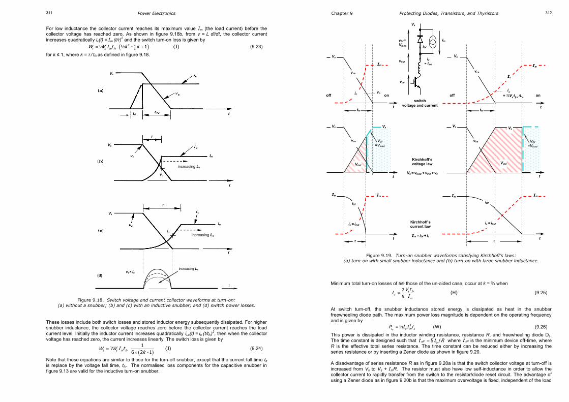
For low inductance the collector current reaches its maximum value Im (the load current) before the collector voltage has reached zero. As shown in figure 9.18b, from v = L di/dt, the collector current
increases quadratically ic(t) = Im (t/τ)2 and the switch turn-on loss is given by
½ ½2 4
3 - 1 (J)t s m fvW V I t k k (9.23)
for k ≤ 1, where k = τ / tfv as defined in figure 9.18.
Figure 9.18. Switch voltage and current collector waveforms at turn-on:
(a) without a snubber; (b) and (c) with an inductive snubber; and (d) switch power losses.
These losses include both switch losses and stored inductor energy subsequently dissipated. For higher
snubber inductance, the collector voltage reaches zero before the collector current reaches the load
current level. Initially the inductor current increases quadratically iLs(t) = io (t/tfv)2, then when the collector
voltage has reached zero, the current increases linearly. The switch loss is given by
1
½ (J)6 2 -1
t s m fvW V I tk
(9.24)
Note that these equations are similar to those for the turn-off snubber, except that the current fall time tfi
is replace by the voltage fall time, tfv. The normalised loss components for the capacitive snubber in
figure 9.13 are valid for the inductive turn-on snubber.
increasing Ls
increasing Ls io
increasing Ls
t
vc× ic (d)
Im
Vs
Vs
Vs
Im
tri
vo
Chapter 9 Protecting Diodes, Transistors, and Thyristors 312
Figure 9.19. Turn-on snubber waveforms satisfying Kirchhoff’s laws:
(a) turn-on with small snubber inductance and (b) turn-on with large snubber inductance.
Minimum total turn-on losses of 5/9 those of the un-aided case, occur at k = ⅔ when
2
9(H)s fv
s
m
V tL
I (9.25)
At switch turn-off, the snubber inductance stored energy is dissipated as heat in the snubber
freewheeling diode path. The maximum power loss magnitude is dependent on the operating frequency
and is given by
½2 (W)
sL s m sP L I f (9.26)
This power is dissipated in the inductor winding resistance, resistance R, and freewheeling diode Ds.
The time constant is designed such that 5 / off st L R
where offt
is the minimum device off-time, where
R is the effective total series resistance. The time constant can be reduced either by increasing the
series resistance or by inserting a Zener diode as shown in figure 9.20.
A disadvantage of series resistance R as in figure 9.20a is that the switch collector voltage at turn-off is
increased from Vs to Vs + ImR. The resistor must also have low self-inductance in order to allow the
collector current to rapidly transfer from the switch to the resistor/diode reset circuit. The advantage of
using a Zener diode as in figure 9.20b is that the maximum overvoltage is fixed, independent of the load
switch
voltage and current
Kirchhoff’s current law
Im = iDf + ic
Kirchhoff’s voltage law
Vs = vload + vind + vc
vo
Im
Vs
vce
t tfv
ic io
Im
Vs
Ic
vce
t tfv
ic = iind
iDf
Im Im
t τ
ic = iind
iDf
Im Im
t τ
vce
Vind
Vs Vs
t
vce
Vind
Vs
Vs
t
VDf
=Vload
VDf
=Vload
Im
ic = iind
vce
vDf = Vload
Vs
vind
iDf
off on off on o
s svf
i
= ½V t /L

Power Electronics 313
current magnitude. For a given maximum overvoltage, the Zener diode absorbs the inductor-stored
energy quicker than would a resistor (see example 7.3 and problem 9.9). The advantages of using
resistive dissipation are lower costs and more robust heat dissipation properties.
Alternatively the Zener diode can be placed across the switch as shown in figure 9.20c. The power
dissipated is increased because of the energy drawn from the supply, through the inductor, during reset.
At higher power, the soft voltage clamp shown in figure 9.20d, and considered in section 9.2, can be
used. At switch turn-off, the energy stored in Ls, along with energy from the supply, is transferred and
stored in a clamp capacitor. Simultaneously energy is dissipated in R and returned to the supply as the
capacitor voltage rises. The advantage of this circuit is that the capacitor affords protection directly
across the switch, but with lower loss than a Zener diode as in figure 9.20c. The energy loss equation for
each circuit is also shown in figure 9.20. In high-voltage applications, the combined features of the soft
clamp in figure 9.20d and the low loss Zener clamp in figure 9.20b can be realised by inserting a series
Zener as shown in the figure 9.20d insert. This avoids the need to series connect Zener diodes, which
would be necessary if the circuit in figure 9.20c were used at voltages above a few hundred volts.
Figure 9.21 shows how a switch turn-on snubber circuit modifies the SOA trajectory during switch-on,
avoiding a condition of simultaneous maximum voltage Vs and current Im.
Figure 9.20. Four turn-on snubber modifications for increasing the rate of release of inductor Ls
stored energy: (a) using a power resistor; (b) using a power Zener diode;
(c) parallel switch Zener diode, VZ > Vs; and (d) using a soft voltage clamp.
Dc
Df Df
Df Df
Dc Dz
Dc
Chapter 9 Protecting Diodes, Transistors, and Thyristors 314
Figure 9.21. The collector I-V trajectory at turn-on with a switching-aid circuit.
Example 9.5: Turn-on air-core inductor snubber design
A 600V, 100A machine field winding is switched at 10kHz. In maintaining a constant field current, the
switch operates with an on-state duty cycle between 5% and 95% (5% ≤ δ ≤ 95%) and has a turn-on
voltage fall time of 100ns, that is, ( ) 600V(1 /100ns)cv t t .
i. Estimate the turn-on loss of the switch.
ii. Design an inductive turn-on snubber using the dimensionally correct identity v = Ldi/dt. What
is the current magnitude in the turn-on inductor when the switch voltage reaches zero. iii. Design an inductive turn-on snubber such that the switch current reaches 100A at the same
time the switch collector voltage reaches zero. In each snubber case, using first a resistor and second a Zener diode for inductor reset, calculate the percentage decrease in switch power dissipation at turn-on, compared to the un-aided case. Solution
i. The switch un-aided turn-on losses are given by equation (9.13). The turn-on time is greater than the voltage fall time (since the current rise time tri has been neglected), thus the turn-on switching losses will be greater than
½ ½= 600V 100A 100ns = 3mJ
3mJ × 10kHz = 30W
on s m on
on on s
W V I t
P W f
ii. Use of the equation v = Ldi/dt results in a switch current that reaches the load current magnitude after
the collector voltage has fallen to zero. From ½ /s m s fv
k L V tI in figure 9.21, k = 3/2 satisfies the
dimensionally correct inductor equation. Substitution into v = Ldi/dt gives the necessary snubber
inductance
100A600V
100ns
= 600 nH
L
L
that is
The snubber inductor releases its stored energy at switch turn-off, and must discharge (demagnetise)
during the switch minimum off-time, offt
. That is
5 /
15% / 5 0.6μH /10kHz
= 0.6
off Lt R
R
R
of
that is
Use the preferred value 0.68Ω (nearest higher preferred value), which reduces the L/R time constant.
vo
io

Power Electronics 315
P(t)
VDf
600V
Example 8.5. part (b) Example 8.5. part (c)
0
tfv
1.5tfv
tfv
0
100A=Area/L
50A
vc=600(1-t/tfv) vc=600(1-t/tfv)
ic=100(t/tfv)2
100A
100A
vind
vind
600V
600V
t t
t t
600V
ic=50(t/tfv)2
100A=Area/L
VDf=Vload
P(t)
The discharge resistor power rating is independent of resistance and is given by
½
2
0.68
2 = ½ 600nH 100A 10kHz = 30W
m sP LI f
The resistor in the circuit in figure 9.20a must have low inductance to minimise voltage overshoot at switch turn-off. Parallel connection of metal oxide resistors may be necessary to fulfil both resistance and power rating requirements. The maximum switch over-voltage at turn-off, (assuming zero resistor inductance), at the commencement of core reset, which is added to the supply voltage, 600V, is
0.68
100A 0.68 68VmV I R
which decays exponential to zero volts in five time constants, 5μs. The maximum switch voltage is 600V
+ 68V = 668V, at turn-off. The reset resistor should be rated at 0.68Ω, 30W, metal film, 750V dc working voltage.
A Zener diode, as in figure 9.20b, of / = 0.6μH×100A/5μs = 12Voffz mV L I t
, will reset the inductor in
the same time as 5 L/R time constants. The switch voltage is clamped to 612V during the 5μs inductor
reset time at switch turn-off. At turn-on when the switch voltage reduces to zero, the snubber inductor current (hence switch current) is less than the load current, 100A, specifically
0
100ns
0
1
1600V 50A
600nH 100ns
indi v dtL
tdt
The switch turn-on loss is reduced from 30W to
2100ns 100ns
0
0 0
2100ns
0
1-100ns 100ns
600V 1- 50A 2.5W100ns 100ns
on s c c s s
s
t tP f i v dt f V i dt
t tf dt
The total turn-on losses (switch plus snubber resistor) are 2.5W + 30W = 32.5W, which is more than the 30W for the unaided switch. Since the current rise time tri has been neglected in calculating the 30W un-aided turn-on losses, it would be expected that 32.5W would be less than the practical un-aided
case. The switch loss is decreased by 92⅔%, (), from 30W down to 2.5W.
Figure 9.22. Solution to Example 8.5.
Chapter 9 Protecting Diodes, Transistors, and Thyristors 316
iii. As the voltage across the switch falls linearly to zero from 600V, the series inductor voltage increases linearly to 600V (k = 1), such that the voltage sum of each component adds to 600V. The inductor current increases in a quadratic function according to
1
( )ind indi t v dtL
The inductor current increases quadratically to 100A in 100ns, as its voltage increases linearly from zero to 600V, that is
100ns
0
1100A 600V
100ns
that is = 300nH
t dtL
L
The necessary reset resistance to reduce the 300nH inductor current to zero in 5μs is
5μs 5 0.3μH / = 0.3Ω
offt R
R
that is
Use the preferred value 0.33Ω in order to reduce the time constant. The power dissipated in the 0.33Ω reset resistor, which is independent of resistance, is
2 2
0.33½ = ½ 300nH 100A 10kHz = 15Wm sP LI f
The resistance determines the voltage magnitude and the period over which the inductor energy is dissipated, not the amount of inductor energy to be dissipated. The inductor peak reset voltage is 100A×0.33Ω = 33V, which is added to the supply voltage of 600V, giving 633V across the switch at turn-off. That is, use a 0.33Ω, 15W metal film (for low inductance), 750V dc working voltage resistor.
A Zener diode, as in figure 9.20b, of / = 0.3μH×100A/5μs = 6Voffz mV L I t
(use 6.8V), will reset the
inductor in the same time as 5 L/R time constants. The switch voltage is clamped to 606.8V during the
5μsofft
inductor reset time at turn-off. The energy dissipated in the switch at turn-on is reduced from 30W to
2100ns 100ns
0 0
2100ns
0
1-100ns 100ns
600V 1- 100A 5W100ns 100ns
on s c c s s m
s
t tP f i v dt f V I dt
t tf dt
The total turn-on snubber losses (switch plus snubber resistor) are 5W+15W = 20W, which is less than
the 30W for the unaided switch. The switch losses, with an inductive turn-on snubber, are decreased by
83⅓%, (), from 30W to 5W.
♣
9.3.4 The polarised turn-on snubber circuit - with saturable ferrite inductance
The purpose of a turn-on snubber circuit is to allow the switch collector voltage to fall to zero while the
collector current is low. Device turn-on losses are thus reduced, particularly for inductive loads, where
during switching the locus point (Vs, Im) occurs in the un-aided transition case.
This turn-on loss reduction effect can be achieved with a saturable inductor in the circuit shown in figure
9.23a, rather than using a non-saturable (air core) inductor as previously considered in section 9.3.3.
The saturable inductor in the snubber circuit is designed to saturate after the collector voltage has fallen
to zero, at point y in figure 9.23. Before saturation the saturable inductor presents high reactance and
only a low magnetising current flows. Once the collector voltage has reached zero, the inductance can
saturate since the switch-on loss period is finished. From Faraday’s equation, assuming the collector
voltage fall to be linear, 1 /s fvV t t , the saturable inductor ℓs must satisfy
d dB
v N NAdt dt
(9.27)
Rearranging, using an inductor voltage ( ) ( ) /s c s fvv t V v t V t t , and integrating gives
0 0
1 1( )
fv fv
fv
t t
s s
t
tB v t dt V dt
NA NA (9.28)
which yields the identity
2
(V)ss
fv
NA BV
t (9.29)
where N is the number of turns,
A is the core area, and
Bs is the core ferro-magnetic material saturation flux density.
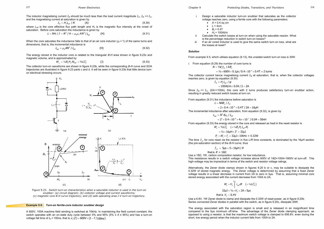
Power Electronics 317
The inductor magnetising current IM should be much less than the load current magnitude Im, IM << Im,
and the magnetising current at saturation is given by
/ (A)M s effI H L N (9.30)
where Leff is the core effective flux path length and Hs is the magnetic flux intensity at the onset of
saturation. Before core saturation the inductance is given by
2 2
0/ / / (H)r eff
L N I N AN L (9.31)
When the core saturates the inductance falls to that of an air core inductor (μr = 1) of the same turns and
dimensions, that is, the incremental inductance is
2
0/ (H)sat effL AN L (9.32)
The energy stored in the inductor core is related to the triangular B-H area shown in figure 9.23c and magnetic volume, and is approximated by
2½ (J)
s s s eff MW B H AL LI ½ (9.33)
The collector turn-on waveforms are shown in figure 9.23b, while the corresponding B-H curve and SOA
trajectories are illustrated in figure 9.23 parts c and d. It will be seen in figure 9.23b that little device turn-
on electrical stressing occurs.
Figure 9.23. Switch turn-on characteristics when a saturable inductor is used in the turn-on
snubber: (a) circuit diagram; (b) collector voltage and current waveforms;
(c) magnetic core B-H curve trajectory; and (d) safe operating area I-V turn-on trajectory.
Example 9.6: Turn-on ferrite-core inductor snubber design
A 600V, 100A machine field winding is switched at 10kHz. In maintaining the field current constant, the
switch operates with an on-state duty cycle between 5% and 95% (5% ≤ δ ≤ 95%) and has a turn-on
voltage fall time of tfv = 100ns, that is, ( ) 600V (1 / )100nsctv t .
energy
tfv
μ0
μ0μr
Bs
B
H
Im IM
Hs t=0
(c) (d)
t
x
y z
x
y
z
x
y
z
Im
IM
IM
minimal
energy
Vs
Chapter 9 Protecting Diodes, Transistors, and Thyristors 318
i. Design a saturable inductor turn-on snubber that saturates as the collector
voltage reaches zero, using a ferrite core with the following parameters.
A = 0.4 sq cm
L = 4cm
Bs = 0.4T
Hs = 100At/m ii. Calculate the switch losses at turn-on when using the saturable reactor. What
is the percentage reduction in switch turn-on losses? iii. If an air cored inductor is used to give the same switch turn-on loss, what are
the losses at reset? Solution
From example 9.5, which utilises equation (9.13), the unaided switch turn-on loss is 30W.
i. From equation (9.29) the number of core turns is
4
½ /
½ 600V 0.1μs / 0.4 10 0.4T 2 turnss fv sN V t AB
The collector current hence magnetising current IM at saturation, that is, when the collector voltages reaches zero, is given by equation (9.30)
/
100At/m 0.04 / 2 2A
M s effI H L N
Since IM << Im, (2A<<100A), this core with 2 turns produces satisfactory turn-on snubber action, resulting in greatly reduced switch losses at turn-on. From equation (9.31) the inductance before saturation is
4
/
2 0.4 10 0.4T / 2A 16μHs ML NAB I
The incremental inductance after saturation, from equation (9.32), is given by
2
0
2 4 7
/
2 0.4 10 4 10 / 0.04 50nH
sat effL N A L
From equation (9.33) the energy stored in the core and released as heat in the reset resistor is
½2
2
½
½ 16μH 2 32μJ32μJ 10kHz = 0.32W
L M s s eff
L L s
W LI B H L A
P W f
The time offt
for core reset via the resistor in five L/R time constants, is dominated by the 16μH section
(the pre-saturation section) of the B-H curve, thus
5μs 5 16μH / = 16Ω
offt R
R
that is
Use a 18Ω, 1W, carbon composition resistor, for low inductance. This resistance results in a switch voltage increase above 600V of 18Ω×100A=1800V at turn-off. This high-voltage may be impractical in terms of the switch and resistor voltage ratings. Alternatively, the Zener diode clamps shown in figures 9.20 b or c, may be suitable to dissipate the 0.32W of stored magnetic energy. The Zener voltage is determined by assuming that a fixed Zener voltage results in a linear decrease in current from 2A to zero in 5μs. That is, assuming minimal core stored energy associated with the current decrease from 100A to 2A,
½2
0
32μJ ½ 2A 5μs 6.4V
offt
L Z ind M
Z
Z
W V i dt LI
V
V
that is
Use a 6.8V, 1W Zener diode to clamp and dissipate the 0.32W of reset power, as in figure 9.20b. Series connected Zener diodes in parallel with the switch, as in figure 9.20c, dissipate 30W. The energy associated with the saturation region is small and is released in an insignificant time compared to the 5μs minimum off-time. The advantage of the Zener diode clamping approach, as opposed to using a resistor, is that the maximum switch voltage is clamped to 606.8V, even during the short, low energy period when the inductor current falls from 100A to 2A.
Power Electronics 319
IM
Im Im
t = 0.1μs
0.4T
100A
2A
0 5μs 5000At/m 100A
100At/m 2A
0
B
t
VZ = 6.8V
t = 0
IM
½BsHs
Example 8.6
H
16μH
50nH
core reset
ii. The switch turn-on losses with the saturable reactor are given by
2100ns 100ns
0 0
2100ns
0
1-100ns 100ns
600V 1- 2A 0.1W100ns 100ns
on s c c s s M
s
t tP f i v dt f V I dt
t tf dt
The switch losses at turn-on have been reduced from 30W to 0.1W, a 99⅔% decrease in losses. The total losses (switch plus Zener diode) are 0.1W + 0.32W = 0.42W, which is significantly less than the 30W in the un-aided case.
Figure 9.24. Solution to Example 8.6. iii. If an air core inductor of 16μH (from part i) were to replace the saturable reactor, the stored energy released would give losses
2
2
½
½ 16μH 100 80mJ80mJ 10kHz = 800W
m
s
W LI
P W f
Clearly the use of an air cored inductor rather than a saturable reactor, to achieve the same switch loss of 0.1W at turn-on, is impractical.
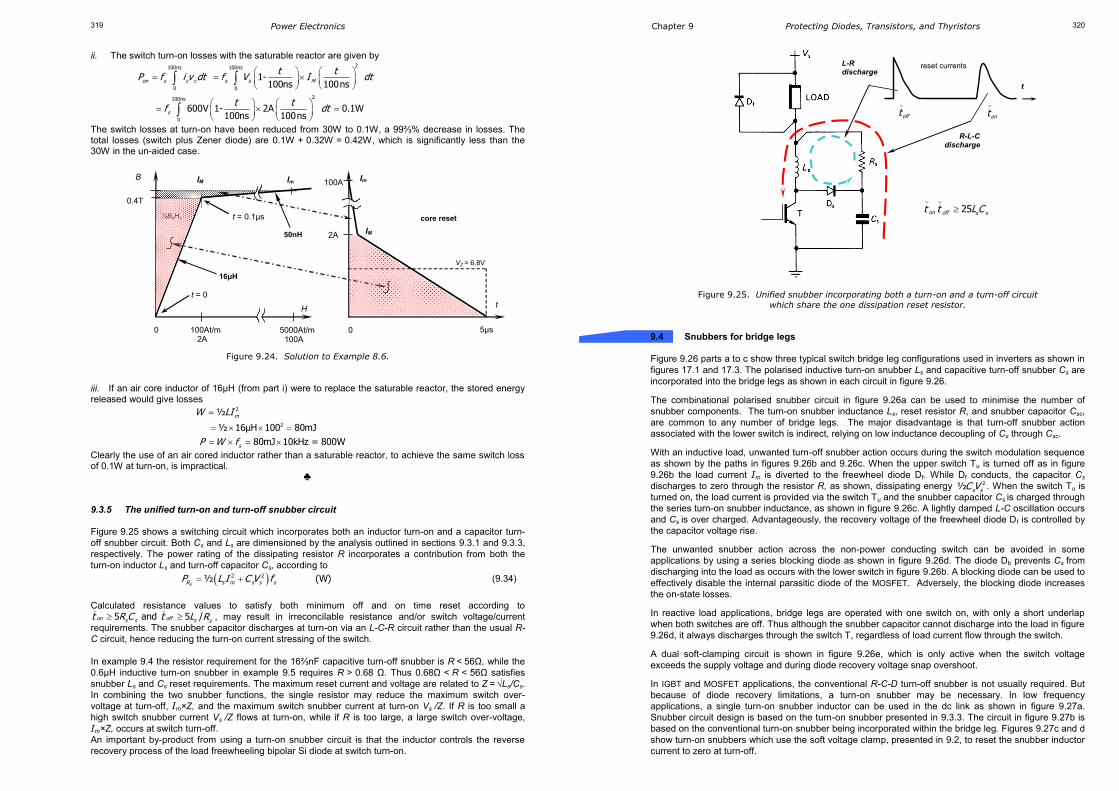
♣ 9.3.5 The unified turn-on and turn-off snubber circuit
Figure 9.25 shows a switching circuit which incorporates both an inductor turn-on and a capacitor turn-
off snubber circuit. Both Cs and Ls are dimensioned by the analysis outlined in sections 9.3.1 and 9.3.3,
respectively. The power rating of the dissipating resistor R incorporates a contribution from both the
turn-on inductor Ls and turn-off capacitor Cs, according to
2 2½ (W)sR s m s s sP L I C V f (9.34)
Calculated resistance values to satisfy both minimum off and on time reset according to
5 and 5 /on offs s s st R C t L R
, may result in irreconcilable resistance and/or switch voltage/current
requirements. The snubber capacitor discharges at turn-on via an L-C-R circuit rather than the usual R-
C circuit, hence reducing the turn-on current stressing of the switch.
In example 9.4 the resistor requirement for the 16⅔nF capacitive turn-off snubber is R < 56Ω, while the 0.6μH inductive turn-on snubber in example 9.5 requires R > 0.68 Ω. Thus 0.68Ω < R < 56Ω satisfies
snubber Ls and Cs reset requirements. The maximum reset current and voltage are related to Z = √Ls/Cs.
In combining the two snubber functions, the single resistor may reduce the maximum switch over-
voltage at turn-off, Im×Z, and the maximum switch snubber current at turn-on Vs /Z. If R is too small a
high switch snubber current Vs /Z flows at turn-on, while if R is too large, a large switch over-voltage,
Im×Z, occurs at switch turn-off.
An important by-product from using a turn-on snubber circuit is that the inductor controls the reverse
recovery process of the load freewheeling bipolar Si diode at switch turn-on.
Chapter 9 Protecting Diodes, Transistors, and Thyristors 320
Figure 9.25. Unified snubber incorporating both a turn-on and a turn-off circuit
which share the one dissipation reset resistor.
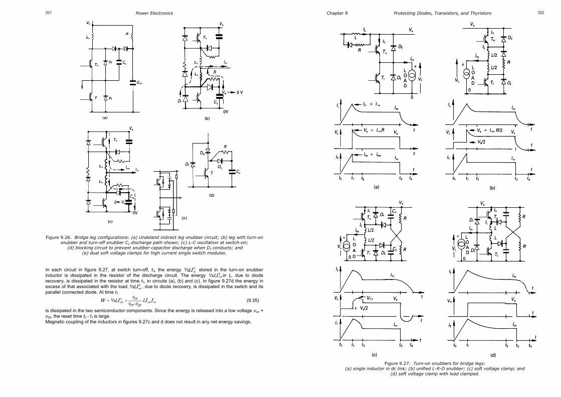
9.4 Snubbers for bridge legs
Figure 9.26 parts a to c show three typical switch bridge leg configurations used in inverters as shown in
figures 17.1 and 17.3. The polarised inductive turn-on snubber Ls and capacitive turn-off snubber Cs are
incorporated into the bridge legs as shown in each circuit in figure 9.26.
The combinational polarised snubber circuit in figure 9.26a can be used to minimise the number of
snubber components. The turn-on snubber inductance Ls, reset resistor R, and snubber capacitor Csc,
are common to any number of bridge legs. The major disadvantage is that turn-off snubber action
associated with the lower switch is indirect, relying on low inductance decoupling of Cs through Csc.
With an inductive load, unwanted turn-off snubber action occurs during the switch modulation sequence
as shown by the paths in figures 9.26b and 9.26c. When the upper switch Tu is turned off as in figure
9.26b the load current Im is diverted to the freewheel diode Df. While Df conducts, the capacitor Cs
discharges to zero through the resistor R, as shown, dissipating energy 2½ s sC V . When the switch Tu is
turned on, the load current is provided via the switch Tu and the snubber capacitor Cs is charged through
the series turn-on snubber inductance, as shown in figure 9.26c. A lightly damped L-C oscillation occurs
and Cs is over charged. Advantageously, the recovery voltage of the freewheel diode Df is controlled by
the capacitor voltage rise.
The unwanted snubber action across the non-power conducting switch can be avoided in some
applications by using a series blocking diode as shown in figure 9.26d. The diode Db prevents Cs from
discharging into the load as occurs with the lower switch in figure 9.26b. A blocking diode can be used to
effectively disable the internal parasitic diode of the MOSFET. Adversely, the blocking diode increases
the on-state losses.
In reactive load applications, bridge legs are operated with one switch on, with only a short underlap
when both switches are off. Thus although the snubber capacitor cannot discharge into the load in figure
9.26d, it always discharges through the switch T, regardless of load current flow through the switch.
A dual soft-clamping circuit is shown in figure 9.26e, which is only active when the switch voltage
exceeds the supply voltage and during diode recovery voltage snap overshoot.
In IGBT and MOSFET applications, the conventional R-C-D turn-off snubber is not usually required. But
because of diode recovery limitations, a turn-on snubber may be necessary. In low frequency
applications, a single turn-on snubber inductor can be used in the dc link as shown in figure 9.27a.
Snubber circuit design is based on the turn-on snubber presented in 9.3.3. The circuit in figure 9.27b is
based on the conventional turn-on snubber being incorporated within the bridge leg. Figures 9.27c and d
show turn-on snubbers which use the soft voltage clamp, presented in 9.2, to reset the snubber inductor
current to zero at turn-off.
t
R-L-C discharge
L-R discharge
reset currents
offt
ont
25on off s st t L C
Power Electronics 321
Figure 9.26. Bridge leg configurations: (a) Undeland indirect leg snubber circuit; (b) leg with turn-on
snubber and turn-off snubber Cs discharge path shown; (c) L-C oscillation at switch-on;
(d) blocking circuit to prevent snubber capacitor discharge when Df conducts; and
(e) dual soft voltage clamps for high current single switch modules.
In each circuit in figure 9.27, at switch turn-off, t3, the energy 2½ mLI stored in the turn-on snubber
inductor is dissipated in the resistor of the discharge circuit. The energy 2½ rmLI in L, due to diode
recovery, is dissipated in the resistor at time t1, in circuits (a), (b) and (c). In figure 9.27d the energy in
excess of that associated with the load, 2½ mLI , due to diode recovery, is dissipated in the switch and its
parallel connected diode. At time t1
2½ rm rm m
ce
ce Df
V
V VW LI LI I
(9.35)
is dissipated in the two semiconductor components. Since the energy is released into a low voltage vce +
vDf, the reset time t2 - t1 is large.
Magnetic coupling of the inductors in figures 9.27c and d does not result in any net energy savings.
Vs
R
Df
Df
Csc
T
Tu
Tu
Tu Ls
Ls
Ls
Ls
Ls
(e)
Chapter 9 Protecting Diodes, Transistors, and Thyristors 322
Figure 9.27. Turn-on snubbers for bridge legs:
(a) single inductor in dc link; (b) unified L-R-D snubber; (c) soft voltage clamp; and
(d) soft voltage clamp with load clamped.
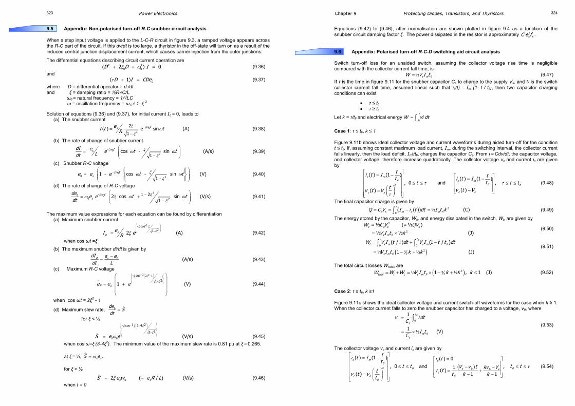
Power Electronics 323
9.5 Appendix: Non-polarised turn-off R-C snubber circuit analysis
When a step input voltage is applied to the L-C-R circuit in figure 9.3, a ramped voltage appears across
the R-C part of the circuit. If this dv/dt is too large, a thyristor in the off-state will turn on as a result of the
induced central junction displacement current, which causes carrier injection from the outer junctions.
The differential equations describing circuit current operation are
2 2
0 0( 2 ) 0D D I (9.36)
and
0
( 1) D I CDe (9.37)
where D = differential operator = d /dt
and ξ = damping ratio = ½R√C/L ω0 = natural frequency = 1/√LC ω = oscillation frequency = ω 0√ 1- ξ
2
Solution of equations (9.36) and (9.37), for initial current Io = 0, leads to (a) The snubber current
2
02
1( ) e sin (A)s te
I t tR
(9.38)
(b) The rate of change of snubber current
2
0-
1 cos - sin (A/s)s tdI e
e t tLdt
(9.39)
(c) Snubber R-C voltage
2
00
1 1 - cos - sin (V)s
te e e t t
(9.40)
(d) The rate of change of R-C voltage
2
0 00 2
- 1 2 2 cos sin (V/s)1
s
tdee e t t
dt
(9.41)
The maximum value expressions for each equation can be found by differentiation
(a) Maximum snubber current
-1
2- cos
1 2 (A) s
p
eI e
R
(9.42)
when cos ωt =ξ
(b) The maximum snubber di/dt is given by
0 (A/s)
p sdI e e
dt L
(9.43)
(c) Maximum R-C voltage
22 11- cos
21 1 (V)o se e e
(9.44)
when cos ωt = 2ξ2 - 1
(d) Maximum slew rate, 0 de
Sdt
for ξ < ½
0 0
1 2- cos 3 4
21
(V/s)S e e
(9.45)
when cos ω=ξ (3-4ξ2). The minimum value of the maximum slew rate is 0.81 pu at ξ = 0.265.
at ξ = ½, .o sS e
for ξ > ½
0
2 ( / ) (V/s)s sS e w e R L
(9.46)
when t = 0
Chapter 9 Protecting Diodes, Transistors, and Thyristors 324
Equations (9.42) to (9.46), after normalisation are shown plotted in figure 9.4 as a function of the
snubber circuit damping factor ξ. The power dissipated in the resistor is approximately 2
s sC e f .
9.6 Appendix: Polarised turn-off R-C-D switching aid circuit analysis
Switch turn-off loss for an unaided switch, assuming the collector voltage rise time is negligible
compared with the collector current fall time, is
½ s m fiW V I t (9.47)
If τ is the time in figure 9.11 for the snubber capacitor Cs to charge to the supply Vs, and tfi is the switch
collector current fall time, assumed linear such that ic(t) = Im (1- t / tfi), then two capacitor charging
conditions can exist
τ ≤ tfi τ ≥ tfi
Let k = τ/tfi and electrical energy
0
t
W vi dt
Case 1: τ ≤ tfi, k ≤ 1
Figure 9.11b shows ideal collector voltage and current waveforms during aided turn-off for the condition
t ≤ tfi. If, assuming constant maximum load current, Im, during the switching interval, the collector current
falls linearly, then the load deficit, Imt/tfi, charges the capacitor Cs. From i = Cdv/dt, the capacitor voltage,
and collector voltage, therefore increase quadratically. The collector voltage vc and current ic are given
by
2
( ) (1 )( ) (1 )
, 0 ,
( )( )
c m
fi c m
fi fi
c sc s
ti t I t
t i t Itt t t
tv t Vv t V
and (9.48)
The final capacitor charge is given by
½2
0( ( )) (C)s s m c m fiQ C V I i t dt I t k
(9.49)
The energy stored by the capacitor, Wc, and energy dissipated in the switch, Wt, are given by
2
2
½ ( ½ )
½ ½ (J)
c s s s
s m fi
W C V QV
V I t k
(9.50)
½ ½
0 0
243
( / ) (1 / )
1 (J)
fit
t s m s m fi
s m fi
W V I t dt V I t t dt
V I t k k
(9.51)
The total circuit losses Wtotal, are
½ ½24
31 , 1 (J)total t c s m fiW W W V I t k k k (9.52)
Case 2: τ ≥ tfi, k ≥1
Figure 9.11c shows the ideal collector voltage and current switch-off waveforms for the case when k ≥ 1. When the collector current falls to zero the snubber capacitor has charged to a voltage, v0, where
½
0
1
1 (V)
fit
o
s
m fi
s
v i dtC
I tC
(9.53)
The collector voltage vc and current ic are given by
2 0 0
( ) (1 ) ( ) 0
, 0 ,1( )
( ) 1 1
c m cfi
fi fis sc
c o fi
fi
ti t I i t
tt t t tV v t kv V
v ttv t v t k k
t
and (9.54)

Power Electronics 325
Figure 9.28. Problem 9.1, GTO thyristor tail current characteristics.
The final capacitor charge is given by
½
0( ( ))
(C)
fi
fi
t
s s m c mt
m fi
Q C V I i t dt I dt
I t k
(9.55)
The energy stored by the capacitor Wc, and energy dissipated in the switch Wt, are given by
½ ½
½
2
2
00
112 0
( )
½ (J)
(1 / ) /
(J)
fi
c s s s
s m fi
t
t m fi fi
m fi
W C V QV
V I t k
W v I t t t t dt
v I t
(9.56)
Using equations (9.53) and (9.55) to eliminate v0 yields
½1
(J)6(2 1)
t s m fiW V I tk
(9.57)
The total circuit losses Wtotal, are
½
2 13
, 1 (J)½
total t c s m fi
k kW W W V I t k
k
(9.58)
The equations (9.50) to (9.52), and (9.56) to (9.58) have been plotted, normalised with respect to
unaided losses ½ s m fiV I t , in figure 9.13.
Reading list
International Rectifier, HEXFET Data Book,
HDB-5, 1987.
Peter, J. M., The Power Transistor in its Environment,
Thomson-CSF, Sescosem, 1978.
Siliconix Inc., Mospower Design Catalog,
January 1983.
Grafham, D. R. et al., SCR Manual,
General Electric Company, 6th Edition, 1979.
Problems
9.1. The figure 9.28 shows GTO thyristor turn-off anode I-V characteristics. Calculate
i. turn-off power loss at 1 kHz. What percentage of the total loss does the tail current account for?
ii. losses when a capacitive turn-off snubber is used and the anode voltage rises quadratically to
600V in 0.5μs. What percentage of the total losses does the tail current account for? What is
the necessary capacitance?
iii. losses when a capacitive turn-off snubber is used and the anode voltage rises quadratically to
600V in 2μs. What percentage of the total losses does the tail current account for? What is the
necessary capacitance? [10.5 W]
Chapter 9 Protecting Diodes, Transistors, and Thyristors 326
9.2. Prove that the minimum total losses (switch plus snubber resistor), associated with a switch
which utilises a capacitive turn-off switching-aid circuit, occur if the snubber capacitor is fully
charged when the collector current has fallen to ⅓ its original value. Derive an expression for this optimal snubber capacitance.
29 (F)m fi
s
s
I tC
V
9.3. Derive an expression for the optimal turn-on switching-aid circuit inductance, assuming the
collector current rise time in the unaided circuit is very short compared with the collector voltage
fall time.
29 (H)s fv
s
m
V tL
I
8.4. A ferrite toroid has B-H characteristics as shown in figure 9.29 and a cross-sectional area, A, of
10 mm2 and effective length, Leff of 50 mm.
Figure 9.29. Problem 9.4, B-H characteristics.
A number of such toroid cores are to be stacked to form a core for a saturable inductor turn-on
snubber in a switching circuit. The circuit supply voltage is V and the switch voltage fall time at
turn-on is tfv. Assume tfv is independent of supply voltage and falls linearly from V to 0 V.
i. Using Faraday’s Law, show that if the ferrite inductor is to saturate just as the switch collector voltage falls to zero at turn-on, then the number of turns N for n cores is given by
2
fv
m
VtN
B An
ii. Derive an expression for the inductance before saturation.
iii. It is required that the maximum magnetising current before saturation does not exceed 1 A.
If only 10 turns can be accommodated through the core window, what is the minimum
number of cores required if V = 200 V and tfv = 1 μs?
iv. How many cores are required if the supply V is increased to the peak voltage of the three-
phase rectified 415 V ac mains, and the load power requirements are the same as in part
iii?
v. Calculate the percentage change in the non-saturated inductance between parts iii and iv.
vi. What are the advantages of saturable inductance over linear non-saturable inductance in
turn-on snubber applications? What happens to the inductance and stored energy after
saturation? [ℓ =N
2/R, n = 5, n = 4, 1:9]
9.5. Prove, for an inductive turn-on snubber, where the voltage fall is assumed linear with time, that
2 1
½ 1
s m
s fv
s m
s fv
L Ik k
V t
L Ik k
V t
for
for
where k = tfv /τ (see figures 9.18 and 9.21).
9.6. Derive the expressions in table 9.1 for a turn-off snubber assuming a cosinusoidal current fall.
Prove equation (9.21), the optimal capacitance value.
Power Electronics 327
9.7 Show that when designing a capacitive turn-off snubber using the dimensionally correct
equation i = Cdv/dt, as in example 9.4b, the capacitor charges to ½Vs when the switch current
reaches zero.
9.8 Show that when designing an inductive turn-on snubber using the dimensionally correct
equation v = Ldi/dt, as in example 9.5b, the inductor current reaches ½Im when the switch
voltage reaches zero.
9.9 Reset of inductive turn-on snubber energy 2½ s mL I can be affected through a resistor, R, as in
figure 9.20a or through a Zener diode, Dz, as in figure 9.20b.
Show that for the same reset voltage, namely Vz=ImR, in each case, Zener diode reset is n
times faster the resistor reset when ons snR C t
.
9.10 In figure 9.12a show that for τ < tfi, the collector current is given by
2 m s s
o m
fi
I V Ci I
t
when the collector voltage reaches the supply voltage rail Vs.
9.11 In figure 9.19a show that for τ < tfv, the collector voltage is given by
2 m s s
o s
fv
I V Lv V
t
when the collector current reaches the load current Im.
9.12 An RCD turn-off snubber is used across a switch in a 600V dc, 10A, 20kHz chopper application.
The switch current fall time at 10A is 100ns.
i. What is the capacitor voltage when the switch current reaches zero at turn-off, if the
switch turn-off loss is to be 1W?
ii. What snubber capacitance is necessary?
For the same un-aided switching conditions, the total losses (switch plus snubber resistor) are to
be (a) 10/3W
(b) 9W
What is the capacitor requirement and what is the capacitor voltage when the switch current
reaches zero?
[600V, 0.83nF]
9.13 For a cosinusoidal current fall at turn-off as shown in figure 9.15, derive expressions for the
switch current io when k < 1 and collector voltage vo when k > 1.
Chapter 9 Protecting Diodes, Transistors, and Thyristors 328
Blank