Power Devices and ICs - Linköping University · –Three-layer bipolar transistors –Thyristors...
59
Power Devices and ICs Chapter 15 Syed Asad Alam DA, ISY 4/28/2015 1
Transcript of Power Devices and ICs - Linköping University · –Three-layer bipolar transistors –Thyristors...

Power Devices and ICs Chapter 15
Syed Asad Alam
DA, ISY
4/28/2015 1
Overview
4/28/2015 2

Overview
• Types of Power Devices – PNPN Thyristor
– TRIAC (Triode Alternating Current)
– GTO (Gate Turn-Off Thyristor)
– BJTs (Bipolar Junction Transistors)
– VMOS (Vertical/V-groov) and DMOS (Double diffused MOS)
– Lateral DMOS (LDMOS)
– IGBT (Insulated Gate Bipolar Transistor)
– BCD (Bipolar CMOS DMOS)
4/28/2015 3

Bipolar Power Devices
• Current carried by both majority and minority carriers
• Include – Two-layer diodes
– Three-layer bipolar transistors
– Thyristors
– TRIACs
– GTO
– Darlington Transistors
– Four+ layer IGBTs
4/28/2015 4

Bipolar Power Devices
4/28/2015 5
Image taken from All About Circuits (www.allaboutcircuits.com)
• BJT (1960s)

Bipolar Power Devices
• BJT [1] (1960s)
– Conceptually same as ordinary BJTs
– Active area distinctly larger Much higher current handling capacity
– Thick and lightly doped collector (1013 cm-3) Large breakdown voltage (as large as 3000 V)
– Structure redesigned to
• Effectively manage power dissipation
• Avoid Kirk effect
4/28/2015 [1] Principles of Electronic Devices by Bart V. Zeghbroeck (University of Colorado Boulder) 6
Bipolar Power Devices
• BJT [1] – Power dissipation is minimized
– Spreading the heat dissipation onto a large area
– Kirk effect avoided by increasing collector doping density
– But for large breakdown voltage devices, Kirk effect avoided by • Low current density of 100 A/cm2
• Large currents – up to 1000 A – obtained by large area device
– SiC devices Hailed as Perfect for high-power BJTs
4/28/2015 [1] Principles of Electronic Devices by Bart V. Zeghbroeck (University of Colorado Boulder)
7

Darlington Transistors[1]
4/28/2015 [1] Principles of Electronic Devices by Bart V. Zeghbroeck (University of Colorado Boulder) 8
Invented at Bell labs by Sidney Darlington in 1953

Darlington Transistors [1]
• Two transistors in an emitter – follower configuration
• Same collector
• Fabricated using same technology as BJT
• Total current gain = Product of current gain of two transistors
• Larger saturation voltage = Forward bias voltage (Q2) + Saturation voltage (Q1)
• Large on-state power dissipation
4/28/2015 [1] Principles of Electronic Devices by Bart V. Zeghbroeck (University of Colorado Boulder) 9

Thyristors[1] (1950s)
• Also called Silicon Controlled Rectifier (SCR)
• 4-layer device with alternating n-type and p-type layers
• Silicon thyristors most common
4/28/2015 [1] Principles of Electronic Devices by Bart V. Zeghbroeck (University of Colorado Boulder) 10

Thyristors[1]
• High power handling capability
• High breakdown voltage
• High gain
• Low on-stage resistance
• Q1 is NPN, Q2 is PNP
• Latching behaviour similar to flip-flop
4/28/2015 [1] Principles of Electronic Devices by Bart V. Zeghbroeck (University of Colorado Boulder) 11

Thyristors[1]
• Operation – Current to gate of Q1 BE junction
of Q1 forward biased Collector current in Q1 Base current to Q2 BE junction of Q2 forward biased Collector current of Q2 Additional base current for Q1
• Transistor can remain ON even if gate current of Q1 is removed
• Lower on-state voltage • Small turn-on current
4/28/2015 [1] Principles of Electronic Devices by Bart V. Zeghbroeck (University of Colorado Boulder) 12

Thyristors[1]
• Disadvantage – Cannot be turned off by just removing gate
current because of latching behaviour
– Power supply needs to be disconnected
– Minority carriers accumulate in base of each transistor
– Need to be removed before reconnecting the power supply
– Slowly ramp the power supply to avoid triggering the thyristor
4/28/2015 [1] Principles of Electronic Devices by Bart V. Zeghbroeck (University of Colorado Boulder) 13
Gate Turn Off (GTO) Thyristor[2]
• Similar to Thyristor
• Used in DC-AC and DC-DC high voltage conversion units
• Turned ON using a signal of positive polarity at gate
• Turned OFF using a signal of negative polarity at gate
• Small gate current must be maintained after turn-on to improve reliability
4/28/2015 [2] Radio-Electronics.com 14

GTO Thyristor
4/28/2015 15

GTO Thyristor[2]
• Turn-On Inject current in base of NPN transistor NPN turns on Collector of NPN turns PNP on PNP on ensures NPN is on (Feedback)
• Turn-Off Negative bias at gate w.r.t. cathode Voltage drop in base Junction reverse bias No current in NPN No current injunction in PNP
• Long switch-off times • Long tail current • Maximum switching frequency 1
KHz
4/28/2015 [2] Radio-Electronics.com 16

TRIAC[1]
• Similar to thyristors in their latching behaviour and multi-layer vertical structure
• Used in AC-powered systems responding similarly to positive and negative applied voltages
• PNPN connected in parallel to NPNP • Additional contact to p-type as well as n-type
gate of the NPNP and PNPN structure respectively
• Additional gate allowes for lowering the threshold for latching
4/28/2015 [1] Principles of Electronic Devices by Bart V. Zeghbroeck (University of Colorado Boulder) 17

TRIAC
4/28/2015 18

Insulated Gate Bipolar Transistors (1980s)
• A combination of DMOS and PNP bipolar device
• Combines high DC current gain, high impedance, low conduction losses and high speed (20 – 100 KHz) of DMOS with high current handling capability and high breakdown voltage of a BJT
• Can be called a voltage controller bipolar device
4/28/2015 19
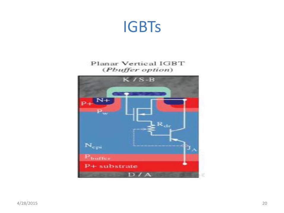
IGBTs
4/28/2015 20

IGBT[1]
4/28/2015 [1] Principles of Electronic Devices by Bart V. Zeghbroeck (University of Colorado Boulder) 21

IGBTs
• Advantages – Low on-state voltage drop – Superior on-state current density – Low driving power – Excellent forward and reverse breakdown capabilities
• Disadvantages – Switching speed in between MOSFET and BJT – Possibility of latchup due to internal PNPN thyristor structure
• Applications – Pulse width modulation servo, three-phase drivers, UPS,
switched mode power supplies and power circuits requiring high switch repetition rates
4/28/2015 22

Power MOSFET Devices (1970s)
• Diverse range of discrete and integrated components – Planar DMOS
– Superjunction DMOS
– Trench DMOS
– LDMOS
– Bulk LDD LDMOS
– RESURF LDMOS
– SOI RESURF LDMOS
4/28/2015 23

Power MOSFET Devices
• Main characteristics – Vertical structure – High-impedance gate drive – Low on-state conduction losses – High frequency (> 1 MHz) switching ability – High off-state breakdowns – Easy paralleling of integrated or multiple discrete devices – Switching speed not limited by minority carrier recombination – Device can mantain a constant current over a wide voltage
range – Drain voltage ratings vary from 3 V for submicron planar devices
to 1200+ V for vertical DMOS – Can survive operation in avalanche like in car’s ABS brakes
4/28/2015 24

Power MOSFET Devices
• A diverse range of devices specified by
– Maximum rated gate and drain voltages
– Channel polarity (N,P, CMOS)
– Construction (planar or trench gate, uniform or DMOS channel)
– Current flow (lateral, vertical, quasi-vertical)
– Threshold voltage including enhancement or depletion mode types
4/28/2015 25

Double Diffused MOSFET (DMOS)
• Characterised by p-type well or body diffused in a low doped n-type drain region
• Dominate high voltage (>100V) designs • Different constructions
– Planar DMOS with a deep-P optional layer – Superjunction DMOS with multi-epi – Trench DMOS with 1-of-n deep-P optional layer – Trench DMOS for charge balance – Lateral DMOS (LDMOS) for high-power RF applications – Lightly Doped Drain (LDD) LDMOS for operations below 20V – Reduced Surace Fields (RESURF) LDMOF and SOI RESURF
LDMOS
4/28/2015 26

Planar DMOS
• P-type well or body • Diffused into a N-epi (drift) • N+ source formed inside the well • Channel formed by inverting p-body • Lightly doped N-epi helps increasing
the breakdown voltage • Source current flows underneath the
gate and vertically through the drain • A short channel device • Lower on-resistance and faster
switching because of vertical structure
4/28/2015 27

Planar DMOS
4/28/2015 28

Planar DMOS
• V-groove and U-groove construction
• Provides high current handling capability and high breakdown voltage
4/28/2015 29

Superjunction DMOS[3]
• A charge compensation structure
• Replaces n-type and p-type regions in the drift layer with alternating p-pillars and n-pillars
• Reduces the normalized on-resistance (RDS.A)
• Active area can be made smaller for same on-resistance
• Enables RDS.QGD to be reduced as well
4/28/2015 [3] Y. Oonishi, Akihiko Ooi and T. Shimatou, “Superjunction MOSFET”, Fuji Electric 30

Superjunction DMOS[3]
• Charge balance needs to be maintained to maintain breakdown voltage
• Impurity concentrations of the n-type and p-type regions must be controlled with precision
• Fabricated using a method of multi-epitaxial growth
4/28/2015 [3] Y. Oonishi, Akihiko Ooi and T. Shimatou, “Superjunction MOSFET”, Fuji Electric 31

Superjuction DMOS[3]
4/28/2015 [3] Y. Oonishi, Akihiko Ooi and T. Shimatou, “Superjunction MOSFET”, Fuji Electric 32
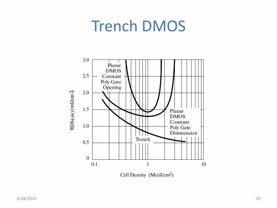
Trench DMOS
• Introduced by Siliconix[4]
• Conducting channel formed vertically along the sidewall of a trench
• Capable of improved on-resistance at high cell densities (1.25 million cells/cm2 )[5]
• Translates into fewer components and enhanced reliability in high-current applications like ABS, power steering, air-conditioning
• Charge balance Trench DMOS similar to superjunction DMOS
4/28/2015 [4] History of FET Technology and the Move to NexFETTM
[5] Richard K. Williams et all., ”Complementary Trecnh Power MOSFETs Define New Levels of Performance” 33

Trench DMOS
4/28/2015 34
Trench DMOS
4/28/2015 35

Laterally Diffused MOS (LDMOS) (1990s)
• Dominant device technology in high-power RF power amplifier applications
• Asymmetric MOSFET for low on-resistance and high breakdown voltage
• Operational frequency range from 10 MHz to 3.8 GHz and voltage range from 28 to 50 V (NXP)
• Provides superior linearity, efficiency, gain and lower cost packaging applications
4/28/2015 36

LDMOS
4/28/2015 37
50V RF LDMOS – White paper by Freescale

LDMOS
4/28/2015 38 50V RF LDMOS – White paper by Freescale

LDMOS
• Different flavours – Lightly doped drain LDMOS (LDD LDMOS) – RESURF LDMOS (reduced surface fields)
• High voltage devices on thin epitaxial layer with low on-resistance
• Voltage range of 20-1200 V • Gives the best trade-off between breakdown voltage and on-
resistance for lateral devices • Peak electric field is reduced to create uniform field
– SOI RESURF LDMOS • Nearly ideal uniform electric field profile is achieved • Monotonically increasing the charge profile from source-to-
drain
4/28/2015 39

LDMOS
4/28/2015 40
High-Voltage and Power ICs
• The ”quiet” revolution Development of high voltage (HVICs) and power ICs (PICs)
• Reuse of legacy submicron digital and ex-DRAM wafer fabs • Integration of disparate analog and digital control with
power devices, programmable logic, memory and sensors • Example PMICs for smartphones integrating 20 linear
and switching regulated voltages with a switching charger • Example HVICs including three phase motor inverter for
air conditioners • Example Miniature universal input AC adapters for USB
phone charging
4/28/2015 41

Bipolar, CMOS and DMOS (BCD) Technology
• Invented by ST in 1980s • Integrates three technologies • Wide used for power integration • Benefits directly from
– CMOS scaling and feature density – Progress made in lateral, quasi- and vertical power devices
through difference constructions • High-density planar and trench gates • Drain engineering using LDD • Multi-RESURF • Superjunction • Shallow and dreep trench isolation etc.
– Integrating two carrier high voltage devices such as IGBTs
4/28/2015 42

BCD
• Some example figures
4/28/2015 43

BCD
4/28/2015 44
BCD
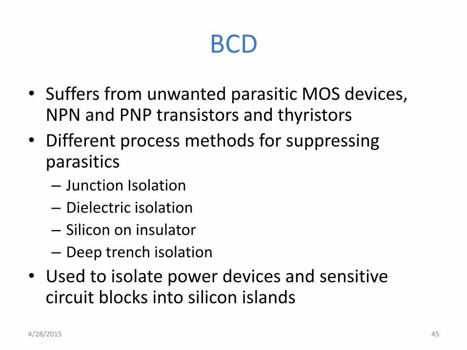
• Suffers from unwanted parasitic MOS devices, NPN and PNP transistors and thyristors
• Different process methods for suppressing parasitics – Junction Isolation
– Dielectric isolation
– Silicon on insulator
– Deep trench isolation
• Used to isolate power devices and sensitive circuit blocks into silicon islands
4/28/2015 45

BCD
• Layout methods include – Locally shorting base-emitter junctions
– Utilizing guard rings, field plates and deep trench isolation in sensitive areas
• Interconnects also a challenge – Need for fine line metal conflicts with thick metal
required by power devices
– Multi-layer metal using a dry-etched thick copper or Al-Cu top layer
– Chip-scale packaging
4/28/2015 46

Selected Paper
• Tsung-Yi Huang et al., ”0.18µm BCD Technology with Best-in-Class LDMOS from 6 V to 45 V,” in Proc. IEEE Int. Symp. on Power Semiconductor Devices and IC’s (ISPSD), pp. 179 – 181, 15 –19 June 2014.
• Proposes a novel nLDMOS structure in BCD technology with multi-oxide in the drift region to reduce the on-resistance at a low cost
4/28/2015 47

Selected Paper
• Conventional LDMOS transistors in BCD suffer from an increase in on-resistance as BVDSS increases
• Performance as such is limited by the fixed oxide thickness in the drift region
• Proposes a two-step-oxide in the drift region
• Thikness near the channel region is thinner than the isolation oxide
• First oxide thickness customized with optimized profile in the drift region
• Achieves best performance between Ron and BVDSS
4/28/2015 48

Selected Paper
4/28/2015 49

Selected Paper
4/28/2015 50

Selected Paper
4/28/2015 51
The potential and impact ionization simulation results of a (a) conventional structure (b) novel structure
Selected Paper
4/28/2015 52
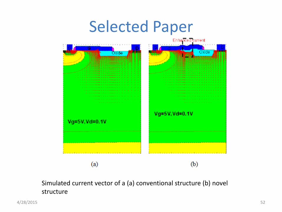
Simulated current vector of a (a) conventional structure (b) novel structure
Selected Paper
4/28/2015 53
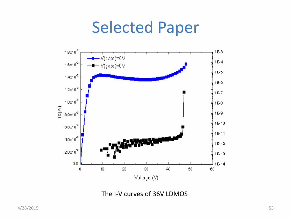
The I-V curves of 36V LDMOS
Selected Paper
4/28/2015 54
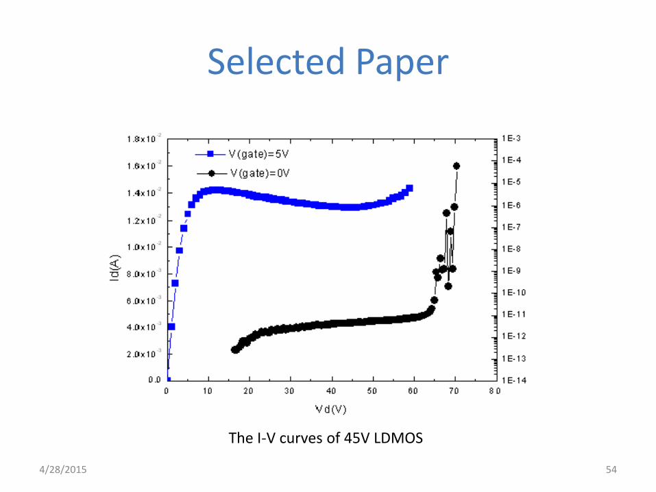
The I-V curves of 45V LDMOS
Selected Paper
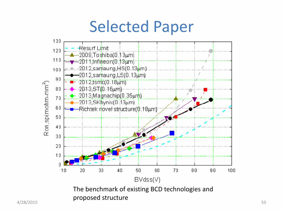
4/28/2015 55
The benchmark of existing BCD technologies and proposed structure

Selected Paper
4/28/2015 56

Wide Bandgap Power Devices
• The electrical and thermal properties of silicon diminish its future prospects
• Small bandgap (1.1 eV) and high leakage currents prohibit operation above 200 C
• Device on-resistance a strong function of electric field
• This electric field of GaN and SiC exceed by around an order of magnitude 10 times the voltage or same voltage at 1/10 device size and 10% resistance
4/28/2015 57

Wide Bandgap Power Devices
• GaN high-electron mobility transistors (HEMT) can substantially improve mobility and reduce resistance
• First WBG devices comprising SiC commercially available from 100 mm wafers
• They include Schottky diodes, BJTs, JFETs, MOSFETs
• GaN devices focus on lower power ratings using lateral FET designs up to 1 kV
• Integrating GaN devices on top of silicon ICs using existing fabrication facilities
• Material, device and fabrication challneges remain
4/28/2015 58

Conclusion
• Different types of power devices exist – Initially bipolar devices used – MOSFETs heralded the dawn of high-frequency gate controlled
power semiconductors – Concepts combined into IGBTs resulting in low conduction
losses, high speed, low on-resistance – Power MOSFETS typically vertical but lateral devices find
application in RF power amplifiers – A number of power devices can be fabricated in the same
technology, called BCD – Wide bandgap devices provide order of magnitude
improvement over silicon devices in terms of temperature, voltage and on-resistance but few devices are commercialized
4/28/2015 59