PROJECT REPORT – 1 1. Project title and summary
82
PROJECT REPORT – 1 1. Project title and summary
Transcript of PROJECT REPORT – 1 1. Project title and summary

PROJECT REPORT – 1
1. Project title and summary

RA
16
11
00
40
10
56
6A
bh
ish
ek P
adh
y
RA
16
11
00
40
10
46
6R
ahu
l B
and
yo
pad
hyay
RA
16
11
00
40
10
45
9A
bh
ish
ek M
adan
RA
16
11
00
40
10
56
3M
ano
swit
a B
hat
ach
arje
e
RA
16
11
00
40
10
48
3S
arik
a
RA
16
11
00
40
10
59
4A
yan
Aro
ra
RA
16
11
00
40
10
74
6R
ou
nak
Gan
gu
ly
RA
16
11
00
40
10
66
2A
bh
inab
a D
utt
a G
up
ta
RA
16
11
00
40
10
57
5T
amo
gh
na
Ch
akra
bo
rty
3D
r.S
hyam
al M
on
dal
Fab
rica
tio
n o
f 2
D m
ater
ial
bas
ed s
atu
rab
le a
bso
rber
fo
r u
ltra
fas
t
fib
er l
aser
s
1D
r. C
hit
tara
nja
n N
ayak
Gra
ph
ene
Ind
uce
d L
on
g t
erm
per
iod
ic d
iele
ctri
c m
ater
ial
2D
r. K
anap
arth
i V
. P
han
i
Ku
mar
Imp
lem
enta
tio
n o
f a
com
pac
t d
ual
ban
d b
and
pas
s fi
lter
on
org
anic
an
d i
no
rgan
ic s
ub
stra
tes
SRM
Inst
itute
of S
cien
ce a
nd T
echn
olog
yC
olle
ge o
f Eng
inee
ring
and
Tec
hnol
ogy
Dep
artm
ent o
f EC
E
AY
201
9-20
20
15
EC
496L
-Maj
or P
roje
ct
Sl N
oR
egis
ter
No
Stud
ents
Nam
e(s)
Proj
ect S
uper
viso
rPr
ojec
t Titl
e
RA
16
11
00
40
10
56
6A
bh
ish
ek P
adh
yG
rap
hen
e In
du
ced
Lo
ng t
erm
per
iod
ic d
iele
ctri
c m
ater
ial
RA
16
11
00
40
10
46
6R
ahu
l B
and
yo
pad
hyay
Dr.
Ch
itta
ran
jan
Nay
ak

SRM
Inst
itute
of S
cien
ce &
Tec
hnol
ogy
Col
lege
of E
ngin
eeri
ng a
nd T
echn
olog
y
Dep
artm
ent o
f Ele
ctro
nics
and
Com
mun
icat
ion
Eng
inee
ring
Proj
ect S
umm
ary
- 201
9-20
20
Sl
N o
Stud
ents
Nam
e Pr
ojec
t G
uide
Pr
ojec
t Titl
e O
bjec
tive
of th
e Pr
ojec
t R
ealis
tic
cons
trai
nts
impo
sed
Stan
dard
s to
be
refe
rred
/ fo
llow
ed
Mul
tidis
cipl
inar
y ta
sks i
nvol
ved
Out
com
e
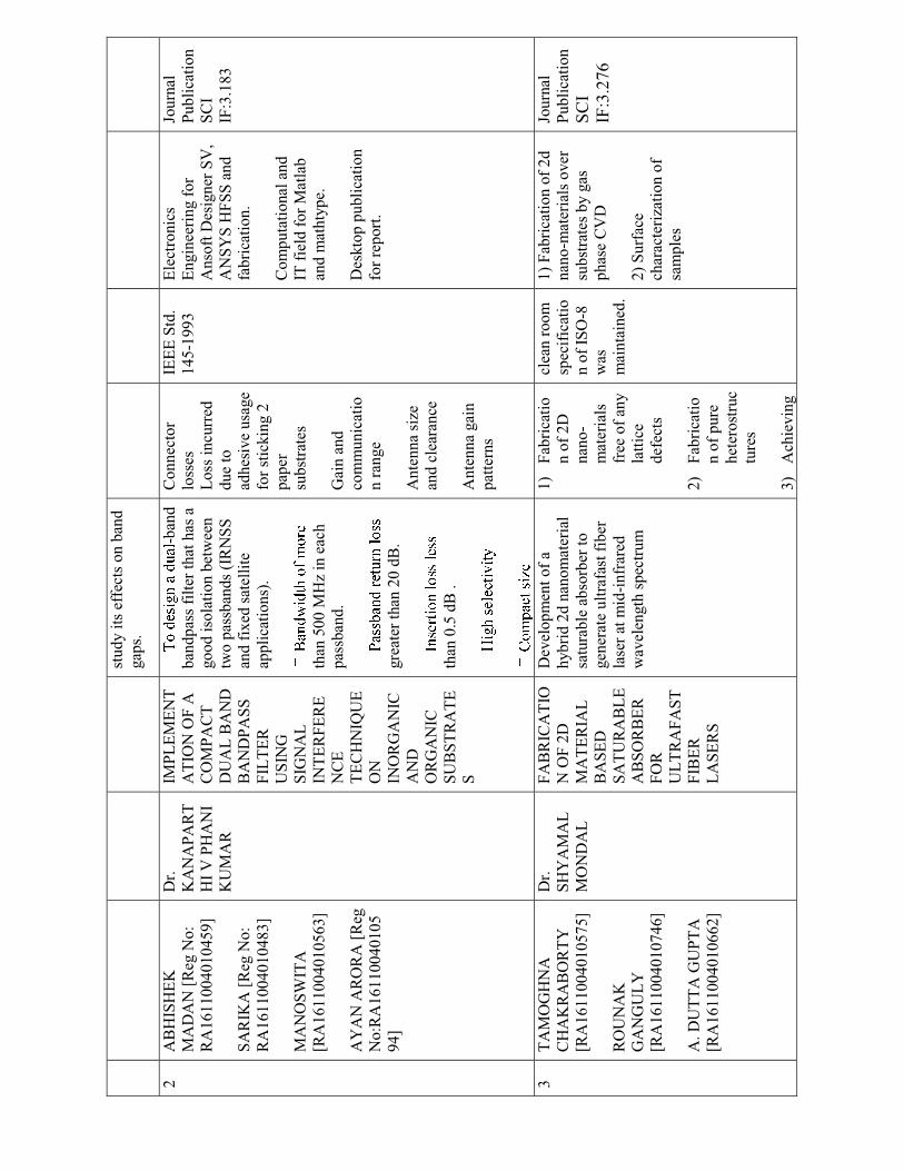
1
AB
HIS
HE
K P
AD
HY
[RA
1611004010566]
RA
HU
L
BA
ND
YO
PA
DH
YA
Y
[RA
1611004010466]
Dr.
Ch
itta
ranja
n
Nay
ak, P
h.D
GR
AP
HE
NE
IND
UC
ED
LO
NG
TE
RM
PE
RIO
DIC
DIE
LE
CT
RIC
MA
TE
RIA
L
e
tran
smis
sion
sp
ectr
a of
Fib
on
acci
, O
cton
acci
,
and
Do
dec
anac
ci
ph
oto
nic
qu
asic
ryst
al
stru
cture
s fo
r p
ote
nti
al
ban
dgap
en
gin
eeri
ng
and
opti
cal
filt
erin
g
appli
cati
ons.
inves
tigat
e lo
cali
zati
on
pat
tern
s fo
r p
ote
nti
al
opti
cal
filt
er
appli
cati
ons.
tran
smis
sion
spec
tra
of
the
mat
eria
l w
ith
var
iati
on
of
inci
den
ce
angle
.
of
layer
s an
d p
rob
abil
ity
of
com
po
siti
on a
nd
Mat
eria
l
con
sist
ency
and
pro
du
ctio
n
cost
ISO
/AN
SI
TC
22
9
IE
C
TC
11
3
1.
Co
mp
uta
tio
nal
and
IT
fie
ld f
or
MA
TL
AB
.
2.
Co
mp
uta
tio
n o
f
Tra
nsf
er M
atri
x
wit
h t
he
hel
p o
f
equ
atio
ns
ob
tain
ed i
n
mat
eria
l sc
ience
.
Journ
al
Pu
bli
cati
on
SC
I
IF:2
.10
6
1A
BH
ISH
EK
PA
DH
YD
r.
GR
AP
HE
NE
eM
ater
ial
ISO
/AN
SI
1.
Co
mp
uta
tio
nal
Jou
rnal
[RA
1611004010566]
Chit
tara
nja
nIN
DU
CE
D
tran
smis
sion s
pec
tra
of
consi
sten
cy
TC
22
9an
d I
T f
ield
fo
rP
ub
lica
tion
Nay
ak, P
h.D
LO
NG
TE
RM
F
ibonac
ci,
Oct
on
acci
,an
d p
roduct
ion
MA
TL
AB
.S
CI
RA
HU
L
PE
RIO
DIC
and
Do
dec
anac
ci
cost
IEC
T
C
IF:2
.10
6
BA
ND
YO
PA
DH
YA
DIE
LE
CT
RIC
ph
oto
nic
qu
asic
ryst
al1
13
2.
Co
mp
uta
tio
n o
f
YM
AT
ER
IAL
stru
cture
s fo
r p
ote
nti
alT
ransf
er M
atri
x
[RA
161100
401
04
66]
ban
dgap
engin
eeri
ng
wit
h t
he
hel
p o
f
and
opti
cal
filt
erin
geq
uat
ions
appli
cati
ons.
ob
tain
ed i
n
mat
eria
l sc
ience
.
inves
tigat
elo
cali
zati
on
pat
tern
s fo
r p
ote
nti
al
opti
cal
filt
er
appli
cati
ons.
tran
smis
sion
spec
tra
of
the
mat
eria
l w
ith
var
iati
on o
f in
cid
ence
angle
.
of
layer
san
d p
rob
abil
ity
of
com
posi
tion
and
stu
dy i
ts e
ffec
ts o
n b
and
gap
s.
2
AB
HIS
HE
K
MA
DA
N [
Reg
No:
RA
1611004010459]
SA
RIK
A [
Reg
No
:
RA
1611004010483]
MA
NO
SW
ITA
[RA
1611004010563]
AY
AN
AR
OR
A [
Reg
No:R
A16110040105
94]
Dr.
KA
NA
PA
RT
HI
V P
HA
NI
KU
MA
R
IMP
LE
ME
NT
AT
ION
OF
A
CO
MP
AC
T
DU
AL
BA
ND
BA
ND
PA
SS
FIL
TE
R
US
ING
SIG
NA
L
INT
ER
FE
RE
NC
E
TE
CH
NIQ
UE
ON
INO
RG
AN
IC
AN
D
OR
GA
NIC
SU
BS
TR
AT
E
S
-ban
d
ban
dp
ass
filt
er t
hat
has
a
good i
sola
tion b
etw
een
two p
assb
ands
(IR
NS
S
and
fix
ed s
atel
lite
app
lica
tio
ns)
.
than
50
0 M
Hz
in e
ach
pas
sban
d.
gre
ater
than
20
dB
.
than
0.5
dB
.
Co
nn
ecto
r
loss
es
Lo
ss i
ncu
rred
du
e to
adh
esiv
e u
sage
for
stic
kin
g 2
pap
er
sub
stra
tes
Gai
n a
nd
com
mu
nic
atio
n r
ange
An
ten
na
size
and
cle
aran
ce
An
ten
na
gai
n
pat
tern
s
IEE
E S
td.
14
5-1
99
3
Ele
ctro
nic
s
En
gin
eeri
ng f
or
An
soft
Des
ign
er S
V,
AN
SY
S H
FS
S a
nd
fab
rica
tio
n.
Co
mp
uta
tio
nal
an
d
IT f
ield
for
Mat
lab
and
mat
hty
pe.
Des
kto
p p
ubli
cati
on
for
rep
ort
.
Journ
al
Pu
bli
cati
on
SC
I
IF:3
.18
3
3
TA
MO
GH
NA
CH
AK
RA
BO
RT
Y
[RA
1611004010575]
RO
UN
AK
GA
NG
UL
Y
[RA
1611004010746]
A. D
UT
TA
GU
PT
A
[RA
1611004010662]
Dr.
SH
YA
MA
L
MO
ND
AL
FA
BR
ICA
TIO
N O
F 2
D
MA
TE
RIA
L
BA
SE
D
SA
TU
RA
BL
E
AB
SO
RB
ER
FO
R
UL
TR
AF
AS
T
FIB
ER
LA
SE
RS
Dev
elo
pm
ent
of
a
hyb
rid
2d
nan
om
ater
ial
satu
rable
ab
sorb
er t
o
gen
erat
e u
ltra
fast
fib
er
lase
r at
mid
-in
frar
ed
wav
elen
gth
spec
trum
1)
Fab
rica
tio
n o
f 2D
nan
o-
mat
eria
ls
free
of
any
latt
ice
def
ects
2)
Fab
rica
tio
n o
f p
ure
het
ero
stru
c
ture
s
3)
Ach
ievin
g
clea
n r
oo
m
spec
ific
atio
n o
f IS
O-8
was
mai
nta
ined
.
1)
Fab
rica
tio
n o
f 2
d
nan
o-m
ater
ials
over
sub
stra
tes
by g
as
ph
ase
CV
D
2)
Su
rfac
e
char
acte
riza
tio
n o
f
sam
ple
s
Journ
al
Pu
bli
cati
on
SC
I
IF:3
.27
6

a b
and
gap
of
0.6
2 -
0.6
5 e
V
for
2 μ
m
radia
tion
4)
Tra
nsf
er
of
2D
nan
o-
mat
eria
l
over
th
e
fib
er t
ip

PROJECT REPORT – 1
2. Project report

GRAPHENE INDUCED LONG TERM PERIODIC
DIELECTRIC MATERIAL
A PROJECT REPORT
Submitted by
ABHISHEK PADHY [RA1611004010566]RAHUL BANDYOPADHYAY [RA1611004010466]
Under the guidance of
Dr. Chittaranjan Nayak, Ph.D(Assistant Professor, Department of Electronics and Communication & Engineering)
in partial fulfillment for the award of the degree
of
BACHELOR OF TECHNOLOGYin
ELECTRONICS AND COMMUNICATION ENGINEERINGof
FACULTY OF ENGINEERING AND TECHNOLOGY
S.R.M. Nagar, Kattankulathur, Kancheepuram District
June 2020

SRM INSTITUTE OF SCIENCE AND TECHNOLOGY(Under Section 3 of UGC Act, 1956)
BONAFIDE CERTIFICATE
Certified that this project report titled “GRAPHENE INDUCED LONGTERM PERIODIC DIELECTRIC MATERIAL ” is the bonafide work of “
ABHISHEK PADHY [RA1611004010566], RAHUL BANDYOPADHYAY[RA1611004010466] ”, who carried out the project work under my super-
vision. Certified further, that to the best of my knowledge the work reported
herein does not form any other project report or dissertation on the basis of
which a degree or award was conferred on an earlier occasion on this or any
other candidate.
SIGNATURE
Dr. Chittaranjan Nayak, Ph.D
GUIDEAssistant Professor
Dept. of Electronics and Communi-
cation & Engineering
Signature of the Internal Examiner
SIGNATURE
Dr. T. Rama Rao, Ph.D
HEAD OF THE DEPARTMENTDept. of Electronics and Communi-
cation Engineering
Signature of the External Examiner

ABSTRACT
This work presents the design proposal of graphene induced photonic multi-
layer structure with quasiperiodic arrangement. It also presents a study of the
transmission spectra of these structures, and investigates properties suitable for
potential bandgap engineering and filtering applications. We employ the trans-
fer matrix method to obtain the transmission spectrum output of multilayer pho-
tonic structure, and use MATLAB to simulate transmission spectrum of various
types of quasiperiodic structures. Specifically, we focus on the Fibonacci se-
quence and its two generalizations, the Octonacci and Dodecanacci sequences,
as well as alternating periodic and pseudorandomly generated sequences. We
choose appropriate generation numbers to approximately equalize the number
of layers in the chosen structures. Finally, we present the plot for transmission
versus reduced frequency for each of the three structures, and highlight areas of
localization and high reflectance, along with contour plots visualizing the vari-
ation of transmission magnitude with incident angle and reduced frequency.

ACKNOWLEDGEMENTS
I would like to express my deepest gratitude to my guide, Dr. Chittaranjan Nayak for his valu-
able guidance, consistent encouragement, personal caring, timely help, and providing me with
an excellent atmosphere for doing research. All through the work, despite his busy schedule,
he has extended cheerful and cordial support to me for completing this research work.
Author
iv

TABLE OF CONTENTS
ABSTRACT iii
ACKNOWLEDGEMENTS iv
LIST OF TABLES vii
LIST OF FIGURES viii
ABBREVIATIONS ix
LIST OF SYMBOLS x
1 INTRODUCTION 1
1.1 Photonic Crystal . . . . . . . . . . . . . . . . . . . . . . . . . . . . . . . . 1
1.2 Types of Photonic Crystal . . . . . . . . . . . . . . . . . . . . . . . . . . . 1
1.3 Photonic-Quasi Crystal and Random PC . . . . . . . . . . . . . . . . . . . 2
1.4 Graphene Induced Photonic Crystal . . . . . . . . . . . . . . . . . . . . . 3
1.5 Photonic Band Gap . . . . . . . . . . . . . . . . . . . . . . . . . . . . . . 3
2 LITERATURE SURVEY 5
3 THEORETICAL FRAMEWORK 7
3.1 Fibonacci Structure . . . . . . . . . . . . . . . . . . . . . . . . . . . . . . 7
3.2 Octonacci Structure . . . . . . . . . . . . . . . . . . . . . . . . . . . . . . 8
3.3 Dodecanacci Structure . . . . . . . . . . . . . . . . . . . . . . . . . . . . 9
3.4 Transfer Matrix Method . . . . . . . . . . . . . . . . . . . . . . . . . . . . 10
3.5 Random Structure . . . . . . . . . . . . . . . . . . . . . . . . . . . . . . . 11
4 MODEL DESIGN AND SPECIFICATIONS 13
5 CODING AND SIMULATION 14
v

5.1 Defining the Parameters . . . . . . . . . . . . . . . . . . . . . . . . . . . . 14
5.2 Defining the Matrix . . . . . . . . . . . . . . . . . . . . . . . . . . . . . . 15
5.3 Output . . . . . . . . . . . . . . . . . . . . . . . . . . . . . . . . . . . . . 16
6 RESULTS 18
6.1 Transmission Spectra . . . . . . . . . . . . . . . . . . . . . . . . . . . . . 18
6.2 Contour Plots . . . . . . . . . . . . . . . . . . . . . . . . . . . . . . . . . 20
6.3 Random Structure Contour . . . . . . . . . . . . . . . . . . . . . . . . . . 22
6.4 Enhanced Graphene-Induced Transmission . . . . . . . . . . . . . . . . . 25
7 CONCLUSION 26
8 FUTURE ENHANCEMENTS 27

LIST OF TABLES
4.1 Generation number and number of layers for different sequences . . . . . . 13
6.1 Details of enhanced transmission due to graphene interface in TE waves . . 24
6.2 Details of enhanced transmission due to graphene interface in TM waves . . 25
vii

LIST OF FIGURES
1.1 Types of PC; (a) 1-D (b) 2-D (c) 3-D . . . . . . . . . . . . . . . . . . . . . 2
1.2 (Left) 1-D photonic quasicrystal, (center) 2-D Penrose photonic quasicrystal,
(right) 3D icosahedral quasicrystal . . . . . . . . . . . . . . . . . . . . . . 2
1.3 1D (left), 2D (center), and 3D (right) random photonic structures . . . . . 3
3.1 Geometric representation of fibonacci photonic multilayer [2] . . . . . . . 8
3.2 Geometric representation of octonacci photonic multilayer [7] . . . . . . . 9
3.3 Geometric representation of dodecanacci photonic multilayer [8] . . . . . . 10
6.2 Contour Plot for (a) Periodic, (b) Fibonacci, (c) Octonacci and (d)Dodecanacci
sequences. . . . . . . . . . . . . . . . . . . . . . . . . . . . . . . . . . . 21
viii

ABBREVIATIONS
PC Photonic Crystal
PQC Photonic Quasi-Crystal
TMM Transfer Matrix Method
TE Transvrse Electric
TM Transverse Magnetic
PBG Photonic Band Gap
GIPBG Graphene Induced Photonic Band Gap
RF Reduced Frequency
TWOG Transmission without Graphene
TWG Transmission with Graphene
ix

LIST OF SYMBOLS
θ Angle of incidence
σg Optical conductivity
Mn Optical transfer matrix
ni Refractive index
Ω Reduced frequency
ω Frequency
c Speed of light
μ Magnetic permeability
ε Electric permittivity
μc Chemical potential of graphene
k Wave vector
di Thickness of layer
x

CHAPTER 1
INTRODUCTION
The study of photonic crystals (PCs) began with the publication of several foundational papers
by E. Yablonovitch[10] and S. John[4] in the late 1980s and 1990s, wherein they studied the
ability of intrinsic semiconductor materials to guide and confine the propagation of light. Arti-
ficial materials of this nature eventually went on to acquire the name photonic crystal (PC) in
the literature. Photonic Crystals have become a interesting field of study due to its frequency
filtering and optical switching applications. They are also employed in thin-film optics and
optical transistors.
1.1 Photonic Crystal
Photonic crystals may be defined as structures with definite periodicity, which are artificially
synthesized using one or more dielectric materials having differing permittivities and refractive
indices. They have been known to exhibit certain interesting properties, such as the ability to
inhibit the emission and propagation of electromagnetic radiation through them. This singular
feature gives rise to what are known as photonic bandgaps, which are frequency ranges with
high reflectivity emerging as a consequence of Bragg scattering.[10]
1.2 Types of Photonic Crystal
Photonic crystals can be classified as one dimensional (1-D), two dimensional (2-D), or three
dimensional (3-D) depending on the direction of layer arrangement (see Fig. 1). One dimen-
sional PCs are dielectric materials arranged periodically only in one direction. Similarly, 2-D
and 3-D PCs are dielectric materials arranged periodically in two and three dimensions respec-
tively. Photonic crystals can also be classified as: (i) Periodic, (ii) Quasi-Periodic or long term
periodic (iii) Random, depending on the arrangement of the constituent dielectric elements

in the structure. Periodic Crystals, as the name suggests, have dielectric layers arranged in a
periodic manner, which are repeated over length.
Figure 1.1: Types of PC; (a) 1-D (b) 2-D (c) 3-D
1.3 Photonic-Quasi Crystal and Random PC
A separate category of related structures, first discovered by Shechtman et al. in 1982, known as
photonic quasicrystals (PQCs) has also attracted significant attention. Unlike photonic crystals,
whose constituent dielectric unit cells have regularly and periodically varying optical proper-
ties, the structure of photonic quasicrystals[1] generally adheres to predefined, deterministic
patterns. In other words, the arrangement of the constituent dielectric materials of Photonic
Quasi-Crystal (PQC) follow some well-defined mathematical substitution rule. Some exam-
ples of substitution rule are the Fibonacci, Octonacci and Dodecanacci sequences. Random
photonic crystals (RPC) do not follow any particular mathematical rule, rather the constituent
materials are arranged random in position.
Figure 1.2: (Left) 1-D photonic quasicrystal, (center) 2-D Penrose photonic quasicrystal,
(right) 3D icosahedral quasicrystal
2

Figure 1.3: 1D (left), 2D (center), and 3D (right) random photonic structures
1.4 Graphene Induced Photonic Crystal
Graphene, well known for its host of remarkable material, physical and chemical properties,
affords great promise for novel scientific investigation and pathbreaking technological appli-
cation. In graphene, monolayers of hybridized carbon atoms are structured and attached in a
hexagonal and crystalline lattice form, giving it a two-dimensional arrangement only one-atom
thick. It is a hundred times stronger than steel, as well as one of the lightest materials known.
In addition to such extraordinary material properties, it also boasts several striking physical
properties, such as high thermal and electrical conductivity, and is a perfect absorber of light.
Graphene is increasingly emerging as an important object in the study of photonic crystals and
photonic quasicrystals. In particular, with graphene being considered as a promising candidate
for use as a photonic crystal component, especially in the terahertz region[9], graphene-induced
Photonic Crystal (PC) and PQC have aroused great scientific interest among researchers re-
cently for a variety of reasons. For instance, recent research shows that multi-layered graphene-
interfaced dielectric structures are highly suitable for terahertz bandgap engineering applica-
tions. Peculiar phenomena associated with the transmission spectra of graphene-induced pho-
tonic multilayer structures in the terahertz range have also become an increasingly attractive
area of study.
1.5 Photonic Band Gap
Band-gaps are regions where light transmission is prohibited[10]. Similarly, photonic band gap
are the range of frequencies where there in no light transmission through the crystal. We will
frequently encounter photonic band gaps Photonic Band Gap (PBG)s later in the results. There
are also bandgaps which are introduced when graphene is inserted into the interface of the struc-
3

ture, these type of bandgaps are known as Graphene Induced Photonic Band Gap (GIPBG)s.
GIPBGs play a major role in these structures as they can be modulated by applying gate voltage
to the graphene layers in the structures. Applying gate voltages changes the chemical poten-
tial of the graphene and modulates the transmission properties of graphene, which is in turn a
consequence of varying band gaps.
4

CHAPTER 2
LITERATURE SURVEY
In this chapter we would like to discuss the results that have already been obtained in the fields
related to the topic. We would like to state a list of work done previously and their inference,
so that the the readers can get a summary of the work done earlier. The list of literature and
their inference/summary are given below-
1. “Inhibited spontaneous emission in solid-state physics and electronics"[10]
Authors: Yablonovitch, E.
Journal: Phys. Rev. Lett. 58, 2059 – Published 18 May 1987
This paper gave us the first foundation and an introduction to photonic crystals and pho-
tonic band gaps. The author proposed that emission in the the material can be modu-
lated/changed by varying the property of the electromagnetic waves used. Lastly, the
property of emission inhibition was studied in detail. These type of band-gap materials
under study was later termed as Photonic Crystals.
2. "Light propagation in quasiperiodic dielectric multilayers separated by graphene"[4]
Authors: Carlos H. Costa, Luiz F. C. Pereira, Claudionor G. Bezerra
Journal: Phys. Rev. B 96, 125412 – Published 8 September 2017
This paper introduces us to the graphene based photonic quasicrystal, in which graphene
is placed at every interface of the crystal structure. The quasi-crystal sequence used
in this paper is the fibonacci sequence. The results showed us that there are bandgaps
introduced in the transmission of the structure due to graphene and occur below a certain
frequency range.
3. "Transmission spectra in graphene-based octonacci one-dimensional photonic qua-sicrystals"[7]
Authors: E.F. Silva, C.H. Costa, M.S. Vasconcelo, D.H.A.L. Anselmo
Journal: Optical Materials. 10.1016/j.optmat.2018.06.031.
The paper introduces us to the octonacci sequence which is a variant of the fibonacci
sequence. Two materials are considered and graphene sheet is introduced at every space
between the layers. The study is done in the high frquency (Terahertz) range.The authors
also vary the chemical potential of the graphene sheets to modulate the photonic bandgap
regions in study. Absorption, Reflection, and Transmission was studied for both TE and
TM waves.

4. "Effects of graphene on light transmission spectra in Dodecanacci photonic qua-sicrystals"[8]
Authors: E.F. Silva, M.S. Vasconcelos, C.H. Costa, D.H.A.L. Anselmo, V.D. Mello
Journal: Optical Materials. 98. 109450. 10.1016/j.optmat.2019.109450.
The paper introduces the Dodecanacci sequence which yet again is a variant of the fi-
bonacci sequence. Two materials were considered in the work and graphene was placed
between the individual layers. TE and TM spectrum was studied in detail and effects
of graphene on photonic band-gap were recorded. Lastly, a varying gate potential was
applied to the graphene sheets to change the chemical potential and hence modulate the
band-gap regions.
5. "Optical properties of periodic, quasi-periodic, and disordered one-dimensional pho-tonic structures"[1]
Authors: Michele Bellingeri, Alessandro Chiasera, Ilka Kriegel, Francesco Scotognella
Journal: Optical Materials. 72. 10.1016/j.optmat.2017.06.033.
This paper takes into account various periodic and quasi periodic sequences and the au-
thors try to study the transmission spectra. The study mainly focuses on how taking
different materials of varying refractive index changes the bandgaps. Additionally, the
variation of transmission spectra when a defect is introduced in one of the materials is
studied and results were published.
6

CHAPTER 3
THEORETICAL FRAMEWORK
This project mainly focuses on comparing the transmission of different structures in the ter-
ahertz range. The dielectric materials under study here follow Fibonacci, Octonacci, Dode-
canacci and random arrangements. Additionally, we also introduce graphene between the inter-
face of the dielectric materials and study the behaviour of transmission spectra when graphene
is introduced. We take five structures with nearly 600 layers each following periodic, Oc-
tonacci, Dodecanacci and random arrangement. Our objective is to study the transmission of
electromagnetic wave by plotting the contour plots of transmission as a function of both inci-
dent angle of wave and reduced frequency. Study of transmission spectra includes the study
of both Transverse Electric (TE) and Transverse magnetic (TM) waves with the frequency of
wave under study is taken in terahertz (1012Hertz)(3.0). In the subsequent sections we will
discuss about the structures, methodology and results in detail.
3.1 Fibonacci Structure
The Fibonacci multilayer structure is constructed by juxtaposing two dielectric layers and,
and arranging the constituent layers according to the Fibonacci sequence. Its nthgeneration
formation is given by the following mathematical relation [2]:
Sn = Sn−1Sn−2
According to the above formula, the nthgeneration of the Fibonacci structure can be obtained
simply by affixing the (n-1)thand (n-2)thgenerations of the structure together, with initial con-
ditions set as S0 = Band S1 = A. Alternatively, the method of construction may also be
represented by a substitution or inflation rule, which explicitly lays out the formation of the
multilayer structure in terms of its constituent elements. It is given below as:
A → AB,B → A

Figure 3.1: Geometric representation of fibonacci photonic multilayer [2]
By following this rule, the first few generations of the Fibonacci structure can therefore
be obtained as follows: S0 = [B], S1 = [A], S2 = [A|B], S3 = [A|B|A]. Since our goal is
to optimize the structures such that the number of layers contained in them is approximately
equal, we consider generation number n = 14 in our work. The corresponding structure consists
of constituent layers.
3.2 Octonacci Structure
Similarly, the construction of the Octonacci multilayer structure also involves appending di-
electric layers and and arranging them according to the Octonacci sequence [7]. The formation
corresponding to generation number ’n’ is mathematically given as:
Sn = Sn−1Sn−2Sn−1, (n ≥ 3)
Initial conditions are set as S1 = Aand S2 = B, and the formula illustrates that for some
generation number , the structure is obtained by attaching two (n-1)thgeneration structures to
one (n-2)thgeneration structure in the manner given in the above mathematical relation. This is
8

more easily shown with the inflation rule:
A → B,B → BAB
Again, we present the structures corresponding to the first few generations for the Octonacci
sequence as follows: S1 = [A], S2 = [B], S3 = [B|A|B], S4 = [B|A|B|B|A|B]. We consider
generation number n = 9 in our work, as the corresponding structure contains constituent layers,
which is quite close to the number of layers contained in the previously considered Fibonacci
structure. The number of elements in the structure can be found out by Pell number
Pn = 2Pn−1 + Pn−2 (3.1)
( initial conditions being P1 = 1, P2 = 1and n≥ 3), so the number of elements in the structure
in the nthstage is given by Pn. The ratio of the number of elements B and A is given by
τ = 1 +√2, given that n→ ∞.
Figure 3.2: Geometric representation of octonacci photonic multilayer [7]
3.3 Dodecanacci Structure
Finally, we arrive at the Dodecanacci structure[8]. Its construction rule is given by the following
mathematical formula:
Sn = (ASn−2Sn−1)2Sn−1, (n ≥ 3)
Here, as with the previous two considered cases, we represent the two dielectric layers
which are to be juxtaposed. The precise manner of juxtaposition is given by the mathematical
9

formula [8] shown above, and is more explicitly illustrated by the following substitution rule:
A → AAAB,B → AAB
For the Dodecanacci structure, we consider generation number 5, which corresponds to
constituent layers. This is suitable for our purposes as it is sufficiently close to the number of
layers contained in our considered Fibonacci and Octonacci structures. The number of elements
in the structure is given by Dn= 4Dn−1- Dn−2 (with D1 = 3and D2 = 11and n≥ 3). The ratio
of Dnto Dn−1is given by τ = 2 +√3, when n→ ∞.
Figure 3.3: Geometric representation of dodecanacci photonic multilayer [8]
3.4 Transfer Matrix Method
In our work we have employed the Transfer Matrix Method (TMM) to evaluate the trans-
mission, absorption and reflection of light through the material. Transfer matrix method is a
mathematical tool used to evaluate the transmission, absorption and reflection of light through
a photonic multilayer by evaluation of matrices of the elements. A matrix is formed for each
dielectric layer and the total Transfer matrix of the the structure is calculated by multiplication
of the individual transfer matrices. The two materials in this work are A (SiO2) , B(TiO2) and
medium C corresponds vacuum. The two important parameters of a multilayer, reflectance (R)
and transmittance (T)[8] [2]can be calculated as:
R =∣∣∣M21
M11
∣∣∣2
10

T =∣∣∣ 1M11
∣∣∣2
Where Mi,j(3.2)corresponds to elements of the transfer matrix. M is calculated for each
structures by finding out the individual element then multiplying them. For instance, for a
fibonacci structure of 2nd generation the transfer matrix becomes -
MT = MCAMAMABMBMBC (3.2)
Which corresponds to structure [AB]. MAand MBcorrespond to layer matrix and MABcorresponds
to the interface matrix and MT stands for total matrix of the multilayer . In thiswork,
MAB,MBA,MBC ,MCB,MAA,MBB
corresponds to interface matrices and MA,MBcorrespond to layer matrices corresponding to
layer A and B. For the graphene interface we need to take into account the optical conductivity
σg = σintra(ω) + σinter(ω)[8][2], which is the sum of the the interband and intraband optical
conductivity and depends on the frequency of operation. Interband frequency will be more
crucial to us due to use of high frequency electromagnetic waves.
3.5 Random Structure
The last structure we are going going to discuss about is the random photonic multilayer[6].
Random structures as stated in the introduction, can be of two types - (i) Random in position,
(ii) Random in width. Random in width photonic crystals consists of periodic multilayer whose
width or thickness is varied according to a probability distribution. In this literature we are only
discussing random in position. Random multilayer (in position) consists of several dielectric
medium arranged without any specific rule or arranged randomly. The number of layers of A
and B in the structure is varied with probability to study the effect of position in the transmis-
sion and bang gaps. There are four structures we consider in the work:
(i) 20% of medium A and 80% of medium B
(ii) 40% of medium A and 60% of medium B
11

(iii) 60% of medium A and 40% of medium B
(iv) 80% of medium A and 20% medium B
All the medium in the four structures are arranged randomly and 600 layers is considered
both with and without graphene .
12

CHAPTER 4
MODEL DESIGN AND SPECIFICATIONS
In this section we will define the layer specifications and the parameters chosen by us. Two ma-
terials Silicon Dioxide (A) and Titanium Dioxide (B) were chosen with refractive indices nA=
1.45 and nB= 2.30 respectively and thickness dA= 10.34 μm, and dB= 6.52 μm. The dimen-
sions are chosen such that they quater-wavelength condition is satisfied. A reduced frequency
of Ω = ωωo
with ωo= 31.4 THz (ωo = 2πcλo
)is selected. Graphene, which inserted at each layer
interface has a frequency dependant optical conductivity σg(ω), and has a chemical potential
μc= 0.2 eV. We selected four structures namely, periodic, Fibonacci, Octonacci, Dodecanacci
and Random with 600, 610, 577, 571, 600 layers respectively which are nearly equal in num-
ber. . Table 4.1 shows the number of layers and generation number of the sequence taken in
our work.
Table 4.1: Generation number and number of layers for different sequences
Sequence Generation Number No. of layersPeriodic - 600
Fibonacci 14 610
Octonacci 9 577
Dodecanacci 5 571
Random - 600

CHAPTER 5
CODING AND SIMULATION
The general scheme followed in this work for simulating various processes and phenomena
associated with electromagnetic propagation through photonic quasicrystal structures using
MATLAB programming may be given as follows.
5.1 Defining the Parameters
First, we define the physical parameters to be used in the simulation of the process and the
mathematical computations involved. This includes a multitude of different variables, such as
central wavelength, thicknesses, refractive indices, permeability constants, conductivity, etc.
These physical constants are basic quantities that are used in the evaluation and computation
of the various mathematical expressions that make up the simulations, therefore defining them
in a manner that circumvents lengthy computation times is very important. Example is given
below -
Code
pi_fv = acos(-1.0d0);
e0 = 8.854e-12;
mu0 = 4.0e-7.*pi_fv;
c = 1.0d0./sqrt(e0.*mu0);
e = 1.602e-19;
hbar = 1.054e-34;
kb = 1.38e-23;
mu = .2d0.*e;
temp = 300.0d0;
beta_fv = mu./(kb.*temp);
lambda0 = 60e-6;

w0 = 2.0d0.*pi_fv.*c./lambda0;
na = complex(1.45d0,0.0d0);
da = lambda0./(4.0d0.*real(na));
nb = complex(2.3d0,0.0d0);
db = real(na./nb).*da;
nc = 1.0d0;
5.2 Defining the Matrix
Secondly, we define the matrices that are used in the transfer matrix method. This section of
the code is especially important since the transfer matrix method lies at the heart of our simu-
lating process; it allows us to compute the outcome of electromagnetic propagation through a
straightforward process of cumulative matrix multiplication. We therefore define the matrices
involved with great care; different sets of matrices are used for TE and TM modes, since the
underlying mathematical variables used are different in the two cases. In defining the matri-
ces, we take into consideration every permutation or configuration of layer arrangement. So
for instance, matrices have been defined for arrangements corresponding to AA, AB, BA, and
BB, as well as for arrangements where interfacing with air is involved, so CA and AC. And of
course, in addition to this, we define the matrices for each type of layer involved, namely A,
B, and C. The equations used for defining these matrices and subsequent mathematical com-
putations have all been taken from various sources in the literature; an extensive theoretical
or mathematical treatment is obviously beyond the scope of the present work. We therefore
provide only a brief outline of the mathematical tools and models used. We then define the
sequences according to which the final output matrix (in accordance with the transfer matrix
method, as discussed above) is mathematically determined. These sequences, as mention in
previous sections, follow deterministic, mathematical rules; the ones used in our work are the
Fibonacci sequence and its three variants, as well as alternating, periodic and non-deterministic,
pseudorandomly generated sequences. The precise mathematical form of the transfer matrix
sequence corresponding to each of the structures considered is determined by the spatial or
physical configuration of the constituent elements present within the structures. Therefore, if
15

in some particular expression we have two constituent elements of the same type appended
to each other, the corresponding mathematical form of the expression will include the corre-
sponding matrices of those two elements multiplied in a sequential manner, and exactly in the
manner as present in the actual photonic quasicrystal structure. The recursive nature of the
mathematical rules used to determine the structure of the crystals makes it convenient to write
down the corresponding mathematical expressions in MATLAB code.
Code
% DEFINITION OF THE MATRIX "MA"
ma(1,1) = exp(-i.*kza.*da);
ma(1,2) = complex(0.0d0,0.0d0);
ma(2,1) = complex(0.0d0,0.0d0);
ma(2,2) = exp(i.*kza.*da);
% DEFINITION OF THE MATRIX "MB"
mb(1,1) = exp(-i.*kzb.*db);
mb(1,2) = complex(0.0d0,0.0d0);
mb(2,1) = complex(0.0d0,0.0d0);
mb(2,2) = exp(i.*kzb.*db);
5.3 Output
Finally, we plot the data embodied in the final output matrix after subjecting it to requisite
manipulations for easy visualization. The very final output of the program is a graph of the
transmission spectrum of the structure. The general scheme described in the present section is
used in all of the simulation programs and for all of the structures. The code to extract output
16

for one of the structures is given below as follows:
Code
%characteristic matrix for a 32-layer periodic stucture.
N=300;
M_T=mca*((ma*mab*mb*mba)^(N-1))*ma*mab*mb*mbc;
% M_T11=M_T(1,1);
% M_T21=M_T(2,1);
t = 1.0d0./abs(M_T(1,1)).^2;
r=(abs(M_T(2,1)./M_T(1,1))).^2;
a = 1.0d0 - t - r;
data_p(kk,cnt)=t;
cnt=cnt+1;
end
end
omega_p=1.0e-20: .01d0: 10.0d0;
omega=(omega_p)’;
load transmitivity.txt
plot(omega,data_p(16,:));
17

CHAPTER 6
RESULTS
The principal outcome of the work conducted over the course of the project comprises the plots
of the transmission spectra obtained as a result of running MATLAB simulations of electromag-
netic radiation in the terahertz range passing through the various photonic quasicrystal struc-
tures discussed in previous sections. The PQC structures considered in our work correspond
to various deterministic mathematical rules that are derived from the well-known Fibonacci se-
quence, as well as periodic and random sequences. The spectra obtained are two-dimensional
plots of two quantities, namely transmission and reduced frequency, which allow us to observe
the transmission of high-frequency electromagnetic radiation for patterns and peculiarities. For
instance, we observe the occurrence of curious behaviour in the form of photonic bandgaps in
the neighbourhood of certain reduced frequencies that may be useful for bandgap engineering
applications. In addition to transmission spectra, we also present contour plots which visualizes
magnitude of transmission as a function of both angle of incidence and reduced frequencies,
which enables us to study the behaviour of electromagnetic radiation through PQC structures
across the full range of frequencies and incidence angles considered in the work, as well as
variation of transmission magnitude with chemical potential. This reveals some striking ob-
servations which will be discussed in the present section, along with all other results already
mentioned and pertaining to the work, and the conclusions which follow. They are given below
as follows.
6.1 Transmission Spectra
We first present in this section a set of transmission spectra for TE waves and contour plots
that show the behaviour of the photonic crystals both at specific angles of incidence and the
full range of incidence angles considered. The former is shown as several plots of transmission
spectra appended together with photonic bandgaps highlighted in each plot.

Figure 6.1: Transmission spectra for TE wave of (a)Periodic, (b) Fibonacci, (c)Octonacci and
(d)Dodecanacci sequences for different angles
19

The reason for choosing specific angles of incidence are as follows: it is observed from
the contour plot (in which we plot transmission as a function of angle of incidence and reduced
frequency, with magnitude of transmission indicated by corresponding shades on a colour spec-
trum) that in certain incidence angle ranges, a striking phenomenon occurs, namely, bandgaps
occurring at certain frequency ranges (in the close neighbourhood of reduced frequencies 2, 4,
6 and 8) are interrupted by small regions of transmission. This phenomenon amounts to what
we consider a “switching effect”, wherein we observe that passing electromagnetic radiation at
exactly the right angle through the PQC structure results in a negation of the photonic bandgap
at certain reduced frequencies. Combining such radiations at different incident angles may
produce outcomes favourable to multiplexing or switching applications. The first set of plots
is shown in Figure [6.1]. Bandgaps are shaded and colour coded in order to distinguish the
underlying reasons for their occurrence. For instance, transmission regions shaded in yellow
correspond to the switching phenomenon described above, and bandgaps shaded in green and
purple represent bandgaps corresponding to graphene-induced bandgaps (GIBGs) and Bragg
gaps respectively. The latter two can be seen to be occurring in all the transmission spectra
and at regular instances, whereas the switching phenomenon occurs only at specific angles
highlighted in the plots in the figure. This is an interesting phenomenon that has heretofore
not been observed in any work, and merits further investigation. Moreover, this occurrence
of this phenomenon can be observed in all of the considered structures, which is also strik-
ing. Notwithstanding the internal configuration of the constituent elements or their pattern of
arrangement, certain features, such as the appearance of bandgaps in the neighbourhoods of
regularly separated reduced frequencies (2, 4, 6, 8), as well as the switching phenomenon, can
be seen occurring in all structures without exception. The specific character of the quasiperi-
odic sequences considered give different transmission spectra, to be sure, but such phenomena
seem to be a constant feature across all the considered structures.
6.2 Contour Plots
We present the contour plots, which as mentioned before, show transmission magnitude plotted
as a function of incidence angle and reduced frequency, with magnitude being indicated by
colour shades on a continuous colour spectrum.
20

Figure 6.2: Contour Plot for (a) Periodic, (b) Fibonacci, (c) Octonacci and (d)Dodecanacci
sequences.
21

This enables us to study the behaviour of electromagnetic transmission through the PQC
structures across the whole range of incidence angles and reduced frequency, which allows
us to obtain a holistic understanding of underlying phenomena. In fact, the contour plots are
what allow us to discern the switching phenomenon, as well as gain interesting insights into
general patterns of behaviour. We plot contour plots for both Transvrse Electric (TE) and
Transverse Magnetic (TM) modes of transmission, for all of the structures, and append them
in a fashion that allows us to see the symmetric nature of the contour plots. As indicated by
the colour spectrum provided adjacent to the contour plots, a darker shade corresponds to a
higher magnitude of transmission, whereas a lighter shade indicates the opposite. This method
of plotting gives us a convenient visualization of the transmission spectra across angles and
frequencies. Type I corresponds to structure without graphene and Type II corresponds to
structure with graphene. Contour plots for different structures under study is presented in Fig.
[6.2]
6.3 Random Structure Contour
In addition to periodic and quasiperiodic structures, we also study the behaviour of random
structures, that is, structures whose internal, constituent elements are arranged according to
some pseudorandomly generated sequence. In such structures also, where we tune the varia-
tion of composition of the two types of elements in accordance with different percentages or
ratios, strikingly similar phenomenon can be observed. Graphene induced photonic bandgaps
can be observed at the same reduced frequencies as in periodic and deterministic, quasiperi-
odic structures, and in some cases, a perceptible “switch” can also be discerned, even though
it is obscured by the reduced magnitude of transmission. The relative feebleness of transmis-
sion in the random cases also suggests that internal configuration, or the particular pattern of
arrangement of internal constituent elements, may be crucial in achieving a higher degree of
transmission. This also merits further investigation. The contour plot of Random Structure is
given in Fig. [6.3]
22

Figure 6.3: Contour Plot for (a) 20% A, (b) 40% A ,(c) 60% A and (d) 80% A sequences, for
different incidence angles
23

Table 6.1: Details of enhanced transmission due to graphene interface in TE waves
Bandgap 1Sequence RF Angle, θ (◦ ) TWOG TWG
Periodic 2.19 45 1.00e-19 0.59
Fibonacci 2.22 47 5.58e-19 0.57
Octonacci 2.17 47 2.75e-17 0.62
Dodecanacci 2.30 52 2.47e-18 0.36
Bandgap 2Sequence RF Angle, θ (◦ ) TWOG TWG
Periodic 4.12 24 8.5e-10 0.6
Fibonacci 4.12 24 4.03e-08 0.55
Octonacci 4.10 25 1.03e-08 0.58
Dodecanacci 4.18 27 1.43e-08 0.64
Bandgap 3Sequence RF Angle, θ (◦ ) TWOG TWG
Periodic 6.08 16 1.22e-06 0.49
Fibonacci 6.09 16 2.06e-05 0.55
Octonacci 6.06 15 2.5e-04 0.493
Dodecanacci 6.12 18 9.15e-06 0.51
Bandgap 4Sequence RF Angle, θ (◦ ) TWOG TWG
Periodic 8.05 11 2.2e-04 0.507
Fibonacci 8.05 11 0.0122 0.48
Octonacci 8.04 11 0.0016 0.401
Dodecanacci 8.07 12 0.0013 0.47
24

Table 6.2: Details of enhanced transmission due to graphene interface in TM waves
Bandgap 1Sequence RF Angle, θ (◦ ) TWOG TWG
Periodic 2.23 50 2.5e-15 0.68
Fibonacci 2.12 33 6.08e-08 0.57
Octonacci 2.05 24 0.0012 0.64
Dodecanacci - - - -
Bandgap 2Sequence RF Angle,θ (◦ ) TWOG TWG
Periodic 4.13, 26 5.1e-10 0.58
Fibonacci 4.05 15 8.8e-04 0.600
Octonacci 4.03 13 0.016 0.58
Dodecanacci - - - -
Bandgap 3Sequence RF Angle,θ (◦ ) TWOG TWG
Periodic 6.08, 16 2.78e-06 0.52
Fibonacci 6.05 12 0.00177 0.55
Octonacci - - - -
Dodecanacci - - - -
Bandgap 4Sequence RF Angle, θ (◦ ) TWOG TWG
Periodic 8.05 11 2.9e-04 0.52
Fibonacci 8.03 8 0.0298 0.46
Octonacci - - - -
Dodecanacci - - - -
6.4 Enhanced Graphene-Induced Transmission
In this section, we present in detail and tabular form the precise regions where the switch-
ing phenomenon, or enhanced transmission due to graphene interfaces, are occurring. As
mentioned several times previously, this phenomenon can be seen to be occurring in all of
the structures and sequences considered, which is a striking observation and outcome of our
present work. The tables contain rows for each of the four structures (all excluding random,
where the effect is noticeably feeble), and each of the tables correspond to the TE or TM mode
of transmission.Reduced Frequency (RF), Angle of incidence θ (◦ ), Transmission without
Graphene (TWOG) , Transmission with Graphene (TWG) are the four information which are
tabulated for four bandgap regions. They are presented in Table 6.1 and 6.2.
25

CHAPTER 7
CONCLUSION
The main focus of the present work has been the study of high frequency, terahertz-range elec-
tromagnetic radiation transmission through photonic quasicrystal structures having periodic,
quasiperiodic and random arrangements. The discussion of results has been centred primar-
ily around the transmission spectra and contour plots of the considered structures, obtained
from conducting a number of MATLAB simulations. From the results of these simulations,
we have gleaned several interesting insights into the nature and general behaviour of electro-
magnetic radiation through photonic quasicrystal structures. The observance of the occurrence
of graphene-induced photonic bandgaps at certain regularly spaced frequencies in all of the
structures considered has been a particularly striking outcome of our work. The occurrence
of anomalous transmission regions within those bandgaps corresponding to specific angles of
incidence is also a remarkable observation that merits further theoretical and practical investi-
gation. The fact that such features have been noticed as being almost constant across the variety
of structures and sequences considered in the present work is highly worthy of discussion. The
use of contour plots as a novel means of visualizing the variation of transmission across entire
ranges of incidence angles and frequencies has allowed us to gain insights and draw conclu-
sions that have previously not been documented in the broad literature of photonic quasicrystal
study. We have considered the behaviour of randomly arranged photonic quasicrystals and the
related transmission and contour plots in our work, which is also a novel step. We have as a
result been able to identify close similarities between the general characteristics of transmission
spectra of quasiperiodic structures and random structures, as well as elucidate key differences.
In summary, we believe our work makes innovative and highly original advances in the study
of photonic quasicrystals and their behaviour.

CHAPTER 8
FUTURE ENHANCEMENTS
In this section we will discuss the future prospects of this project. Until now we have varied the
angle of incidence and changed the layer positions randomly by applying different probability
of composition, to study the their effects on PBG and GIPBG . The future works we would like
to propose -
� Varying the temperature to study the effects of temperature on photonic and graphene
induced bandgaps
� Changing chemical potential of graphene sheets by applying gate voltage to individual
graphene sheets.
� Varying the width of individual crystal according to a probability distribution (layer width
modulation), these type of structures are called random-in-width PC.

REFERENCES
[1] Bellingeri, M., Chiasera, A., Kriegel, I., and Scotognella, F. (2017). “Optical properties
of periodic, quasi-periodic, and disordered one-dimensional photonic structures.” OpticalMaterials, 72.
[2] Costa, C., Pereira, L., and Bezerra, C. (2017). “Light propagation in quasiperiodic dieletric
multilayers separated by graphene.” Physical Review B, 96.
[3] Fuentecilla-Carcamo, I., Palomino-Ovando, M., and Ramos-Mendieta, F. (2017). “One di-
mensional graphene based photonic crystals: Graphene stacks with sequentially- modulated
doping for photonic band gap tailoring.” Superlattices and Microstructures, 112.
[4] John, S. (1987). “Strong localization of photons in certain disordered dielectric superlat-
tices.” Phys. Rev. Lett., 58, 2486–2489.
[5] Nayak, C., Aghajamali, A., Alamfard, T., and Saha, A. (2017). “Tunable photonic band
gaps in an extrinsic octonacci magnetized cold plasma quasicrystal.” Physica B CondensedMatter, 525, 41–45.
[6] Nayak, C., Costa, C., and Aghajamali, A. (2019). “Robust photonic bandgaps in quasiperi-
odic and random extrinsic magnetized plasma.” IEEE Transactions on Plasma Science, 47,
1726–1733.
[7] Silva, E., Costa, C., Vasconcelos, M., and Anselmo, D. (2018). “Transmission spectra in
graphene-based octonacci one-dimensional photonic quasicrystals.” Optical Materials.
[8] Silva, E., Vasconcelos, M., Costa, C., Anselmo, D., and Mello, V. (2019). “Effects of
graphene on light transmission spectra in dodecanacci photonic quasicrystals.” Optical Ma-terials, 98, 109450.
[9] Tassin, P., Koschny, T., and Soukoulis, C. (2013). “Graphene for terahertz applications.”
Science, 341, 620–621.
[10] Yablonovitch, E. (1987). “Inhibited spontaneous emission in solid-state physics and elec-
tronics.” Phys. Rev. Lett., 58, 2059–2062.
[10] [1] [7] [2] [8] [3] [6] [5] [4] [9]
28


������������ ���
��� � ��������
����������� �
������ ������
� ��
� ��
� ��
� ���
� ���
� ���
����� !"��
��#� ��������
������������
�$%&'(�)*��'(+$,��- .�/*��*���%� %$,��&$-0 '!'%
#*���.�%%$*�1� "�+�2%'2$"$+ '!� !�3-$( 2�% '0 �
0 �&��+% ��4-&+ &$5�%(�(�2$%$+�0�65�"%$2��!�1,
��5( �$&��7 �8��,��9�:�-6& �$+ '!
�$(('! ,��-�$,��- " !'��% $!+�,�/%$!��(�'
/-4$"$&& ,�/%$!��(�'���'+'"!�&&$,�#-"& �&4'
�$!.$! ,�$!0�/$6 '�� �/'!.'*�1��&;<�((�46&�0
) �%$%�� �$&� $!'(+%-�+-%�(�;'%�) "���;; � �!�5
�'%'-(���'+'! �(��%5(+$&(1,����� $!'�-6& �$+ '!
%�*2-6& �*2'& 4 * +�!+�%!�+��'-%��
888*='-%!$&+'�(*$�*-��!+�%!�+��'-%��
�-64 ++�0�+'��! 7�%( +5�';��'&&�"���'%��+-0�!+��$2�%
�-64 ++�0�+'��! 7�%( 0$0��'& +>�! �$�0���$0% 0�+-0�!+��$2�%

: ���
? ���
@ ���
�9 ���
�� ���
�� ���
�A�&-0��3-'+�( �;; �A�&-0��4$+���( �����8'%0(
�-64 ++�0�+'��!0 $!��!(+ +-+��';����!'&'"5,
B�$%$"2-%��+-0�!+��$2�%
�*/*�� &7$,��*)*��'(+$,��*�*�C$(�'!��&'(,
�*)*�*�*��!(�&4'*�1%$!(4 (( '!�(2��+%$� !
"%$2��!�<6$(�0�'�+'!$�� �'!�<0 4�!( '!$&
2�'+'! ��3-$( �%5(+$&(1,��2+ �$&��$+�% $&(,��9�@�-6& �$+ '!
�� ++$%$!=$!� $5$�*�1�'0��$!$�� ��A+% !( �
4$"!�+ .�0�2&$(4$�4-&+ &$5�%1,��2+ �$&
�$+�% $&(,��9�9�-6& �$+ '!
�4 %��$0$! ,��$4$0�'(�$!��!+�.$%*�1�2+ �$&
2%'2�%+ �(�';�'!�<0 4�!( '!$&�2�'+'! ���%5(+$&(
�'!+$ ! !"�"%$2��!��(���+(1,���5( �$��D
�'!0�!(�0��$++�%,��9���-6& �$+ '!
����C$(�'!��&'(*�E'-%!$&�';���5( �(
�'!0�!(�0��$++�%,�9:F9�F�@@?�-6& �$+ '!
�-64 ++�0�+'�'66��! 7�%( +5�';���'!'4 �(�G
���!'&'"5�+-0�!+��$2�%

�A�&-0��6 6& '"%$2�5 �!

/� ���#���
F9
����� !"��
#�����B����
#� ��������� �
���������
��#���
��#���
��#���
��#���
��#���
��#���
��#��:
��#��?
��#��@
��#���9
��#����
��#����
��#����
��#����
��#����
��#����
��#���:
��#���?
��#���@
��#���9

��#����
��#����
��#����
��#����
��#����
��#����
��#���:
��#���?
��#���@
��#���9
��#����
��#����
��#����
��#����

PROJECT REPORT – 1
3. Publication

Research Article Vol. 37, No. 12 / December 2020 / Journal of the Optical Society of America B 3801
Enhanced transmission induced by embeddedgraphene in periodic, quasiperiodic, and randomphotonic crystalsAbhishek Padhy,1 Rahul Bandyopadhyay,1 Carlos H. Costa,2Claudionor G. Bezerra,3 AND Chittaranjan Nayak1,*1Department of Electronics andCommunication Engineering, College of Engineering and Technology, SRM Institute of Science and Technology,SRMNagar, Kattankulathur, Kanchipuram, Chennai, TN 603203, India2Universidade Federal do Ceará, Campus Avançado de Russas, 62900-000, Russas-CE, Brazil3Departamento de Física Teórica e Experimental, Universidade Federal do Rio Grande doNorte, Natal-RN 59078-900, Brazil*Corresponding author: [email protected]
Received 8 July 2020; revised 13 October 2020; accepted 15 October 2020; posted 16 October 2020 (Doc. ID 402357);published 18 November 2020
The study of photonic crystals, artificial materials whose dielectric properties can be tailored according to thestacking of their constituents, remains an attractive research field, and it is the basis of photonic devices based onthe generation, processing, and storage of photons. In this paper, we employ a transfer-matrix treatment to studythe propagation of light waves in periodic, quasiperiodic (Fibonacci, Octonacci, and Dodecanacci), and randomdielectric multilayers with graphene embedded. The structures considered here are composed of two buildingblocks, silicon dioxide (building block A = SiO2) and titanium dioxide (building block B = TiO2). We calculatetheir transmission spectra as a function of incident angle θ and reduced frequency �. Our main goal is to investigatethe enhancement of the transmission due to the presence of graphene. In particular, we show that bandgap regionsbecome passband regions when graphene is embedded in the optical multilayers. More specifically, for a rangeof the incident angle θ and reduced frequency �, the PCs with graphene embedded display an unexpected prop-erty: the electromagnetic radiation is transmitted mainly through the multilayers and not reflected or absorbed asexpected for large structures. ©2020Optical Society of America
https://doi.org/10.1364/JOSAB.402357
1. INTRODUCTION
The study of photonic crystals (PCs) started in 1987 with theindependent seminal works of E. Yablonovitch [1] and S. John[2]. Those authors investigated the capability of semiconductormaterials to guide and confine the propagation of light. PCsmay be defined as structures consisting of alternating layers oftwo or more different dielectric materials, so that the artificiallysynthesized structure as a whole presents a spatially periodicpermittivity function [3]. In recent years, a lot of research efforthas been made towards the understanding and applications ofPCs, concerning fabrication [4], prisms [5], lenses [6–9], filters[10,11], photonic quasiperiodic fibers (PQFs) [12–18], sensors[19], metasurfaces [20], surface waves [21], etc. Among all veryinteresting properties presented by PCs, one in particular makesthese systems excellent options for technological applicationsand attractive objects of research: the emergence of frequencyregions, named photonic bandgaps (PBGs), for which there isno emission or propagation of electromagnetic waves throughthe structure [22,23]. As a consequence, PCs work as high
reflectivity mirrors [24]. Usually the most common way for theformation of a PBG is Bragg scattering (conventional PBG)because it can occur in any photonic system [25]. However,PBGs can also be formed by the zero average refraction index(n̄ = 0 PBG) or phase conditions (φ̄ = 0 PBG), for example,in left-handed materials (LHMs) [26]. Finally, when the PCpresents a surface optical conductivity, a PBG can emerge aswell. For instance, one can observe a graphene induced PBG(GIPBG) in PCs with embedded graphene [27].
Parallel to these developments in the field of PCs, the proper-ties of a special and interesting class of structures, first discoveredby Shechtman et al. [28] in 1984 and known as quasiperiodiccrystals or quasicrystals (QCs), have been also widely investi-gated. One of the most important reasons is that they can bedefined as an intermediate state between an ordered crystal(their definition and construction follow purely deterministicrules) and a disordered solid (many of their physical propertiesexhibit an erratic-like appearance) [29,30]. Hence, QCs presentforbidden symmetries by classical crystal rules and long-range
0740-3224/20/123801-08 Journal © 2020Optical Society of America

3802 Vol. 37, No. 12 / December 2020 / Journal of the Optical Society of America B Research Article
correlation order [31]. When the alternating layers composingthe PC are arranged according to a quasiperiodic sequence(with a well-defined mathematical substitution rule), so thatthe constituent dielectric function varies quasiperiodically,we have the so-called one-dimensional (1D) photonic QCs(1DPQCs) [32,33]. On the other hand, if the alternating layerscomposing the PC are arranged in a random fashion, for exam-ple, by following some probability function such as a Gaussiandistribution [34,35], we have a 1D random PC (1DRPC),for which disorder-induced localization, delocalization, andinter-transition effects can be observed [36,37].
Graphene, the two-dimensional allotropic form of the carbonwhere atoms with s p2 hybridization are strongly and denselyattached creating a planar hexagonal crystalline lattice, has beenhailed by many as the new silicon of the 21st century. This mate-rial is nearly 200 times stronger than steel, flexible, good for lightabsorption, and highly conductive to heat and electricity. Withthose remarkable physical properties, graphene is currently inthe scientific limelight not only for possessing tremendous tech-nological potential but also for having opened several avenues ofbasic science exploration [38,39]. Recently, a new and interest-ing research field, called graphene nanophotonics (GN) [40,41],has emerged. GN deals with optical systems in which grapheneis integrated in the structure under investigation, usually withmaterials that operate in the terahertz frequency region [42]. Inparticular, 1D graphene-based PCs and PQCs have attractedinterest from researchers because they are highly suitable forterahertz bandgap engineering applications [27].
In the present work, we intend to investigate more deeply theeffects of inserting graphene at the interfaces of two different—non-dispersive and non-magnetic—dielectric layers (labeledas A and B) in 1D PCs (1DPCs). The structures were numer-ically investigated by employing the powerful transfer-matrixmethod (TMM), which simplifies the algebra [27,43]. Theoptical multilayers considered in this work are spatially arrangedaccording to a periodic sequence, quasiperiodic sequences (suchas Fibonacci [34], Octonacci [44], and Dodecanacci [45]), andalso random sequences [46]. One should remark that, unlikewhat was done in previous works, we choose some specific gen-erations for each sequence (periodic, quasiperiodic, or random)to obtain similar multilayer sizes [34,47]. Later, we give moredetails about the structures considered here.
This work is organized as follows. In Section 2, we presentthe physical model based on the TMM to solve the Maxwell’sequations for electromagnetic waves in 1D graphene-based PCs.The physical parameters considered here as well as the numericalresults are presented and discussed in detail in Section 3. Finally,our findings are summarized in Section 4.
2. PHYSICAL MODEL AND TRANSFER-MATRIXMETHOD
The materials considered in this work are silicon dioxide (SiO2),denoted by A, titanium dioxide (TiO2), denoted by B , vac-uum, denoted by C , and graphene, represented by its opticalconductivity σg . The system is schematically presented inFig. 1, where we present a periodic 1DPC consisting of alter-nating unit cells A|B juxtaposed to form the periodic finitearray |A|B |A|B | · · · |A|B |. This array is surrounded by a
Fig. 1. Schematic representation of the 1DPC showing slabs A andB , incident and emergent media C , and graphene at the A|B and B |Ainterfaces.
semi-infinite media C , which is considered to be vacuum. Thephysical parameters of the optical media are the thicknesses(dA and dB ) and dielectric permittivities (εA, εB , and εC ).
The graphene embedded at the interfaces is modeled by afrequency-dependent conductivity σg (ω) composed of twocontributions: (i) the intraband σ intra
g (ω) (related to the scat-tering from phonons, electrons, and impurities); and (ii) theinterband σ inter
g (ω) (related to the electron–hole recombi-nation) [48]. The explicit form of the graphene’s surfaceconductivity is given by [49]
σg (ω) = σ intrag (ω) + σ inter
g (ω), (1)
with
σ intrag (ω) = i
e 2
π� (�ω + i�)
{μc + 2kB TK ln
[e (−μc /kB TK ) + 1
]}(2)
and
σ interg (ω) = i
e 2
4π�ln
[2 |μc | − (�ω + i�)
2 |μc | + (�ω + i�)
]. (3)
Here e is the electronic charge, � is the Planck’s constant, kB
is the Boltzmann’s constant, TK is the temperature in Kelvin,� is the damping constant of graphene, and μc is the chemi-cal potential (which can be controlled by the gate voltage). Itis known from the literature that for �ω much smaller thanthe chosen chemical potential, the interband contribution isneglectable [48]. As a consequence, the light propagation will bemore affected by the presence of graphene in the low frequencyregion, as was shown by Costa et al. [27].
A quasiperiodic structure can be experimentally constructedby juxtaposing two building blocks A and B followingFibonacci, Octonacci, and Dodecanacci sequences (seeRef. [50]). A Fibonacci sequence SN is generated by appendingthe N − 2 sequence to the N − 1 one, i.e., SN = SN−1SN−2
(N ≥ 2). This construction algorithm requires initial conditionschosen as S0 = B and S1 = A. The Octonacci sequence growsin such a way that its Nth stage is iteratively given by the ruleSN = SN−1SN−2SN−1, for N ≥ 3, with S1 = A and S2 = B .Finally, the Nth generation of the Dodecanacci sequence can beiteratively obtained by the rule SN = (ASN−2SN−1)
2SN−1, forN ≥ 3, with S1 = A AB and S2 = (AS1)
2S1. Figure 2 schemati-cally illustrates the inflation rules of the quasiperiodic sequencesconsidered here.
Here we have chosen periodic, quasiperiodic, and randomstructures with similar sizes for comparison purposes (around600 slabs), the 14th Fibonacci generation (610 slabs), the ninth

Research Article Vol. 37, No. 12 / December 2020 / Journal of the Optical Society of America B 3803
(a)
A
A B
A B A
A B A A B...
(b)
A
B
B A B
B A B B B A B...
...
(c)
A A B
A A A B A A A B A A B
Fig. 2. Schematic illustration of the inflation rules for (a) Fibonacci,(b) Octonacci, and (c) Dodecanacci sequences.
Table 1. 1D Structures Considered in this Work
Name of the Sequence Generation Number Number of Layers
Periodic – 600Fibonacci 14 610Octonacci 9 577Dodecanacci 5 571Random – 600
Octonacci generation (577 slabs), and the fifth Dodecanaccigeneration (571 slabs), as summarized in Table 1. Regardingthe periodic structure, the unit cell is repeated 300 times so thatwe get a structure with equivalent size, i.e., 600 slabs. For therandom sequence, we use a random number generator functionthat chooses between two letters, A and B , and create a chainwith 600 of these letters, considering a given probability ofoccurrence of the letter A, p(A). For each value of p(A), weconsider four random sequences, which has been found to be areasonable minimum quantity to obtain reliable conclusions.
We consider that a transverse electric (TE or s ) or magnetic(TM or p) polarized monochromatic electromagnetic wave,traveling from left to the right in vacuum with angular frequencyω and wave-vector �k = (kx , kz), obliquely reaches the photonicmultilayer (distributed along z direction) at an angle θ fromthe normal (see Fig. 1). For the multilayer system consideredhere, whose unit cell is repeated n times, the transfer-matrix Mn
that relates the amplitude of the electromagnetic wave at theinterfaces is given by [27]
Mn = (MA MB )n =(∏
Mj
)n, (4)
with
MTEj (d j , ω)
=⎡⎣ cos(kzjd j )
(i
q j
)sin(kzjd j )
σg cos(kzjd j ) + iq j sin(kzjd j ) cos(kzjd j ) +(
iσg
q j
)sin(kzjd j )
⎤⎦(5)
and
MTMj (d j , ω)
=[
cos(kzjd j ) − iσg q j sin(kzjd j ) −σg cos(kzjd j ) +(
iq j
)sin(kzjd j )
iq j sin(kzjd j ) cos(kzjd j )
].
(6)
Here q j = − kzjωμ0
(for TE waves), and q j = kzjωε0ε j
(for TM
waves). Also, kzj is the z component of the wave-vector withinmedium j ( j = A or B), which is given by
kzj =⎧⎨⎩
[ε j (ω/c )2 − k2
xC
]1/2, for ε j (ω/c )2 ≥ k2
xC,
i[k2
xC − ε j (ω/c )2]1/2, for ε j (ω/c )2 < k2
xC,
(7)
where ε j is the dielectric constant of medium j , c is the speedof light in vacuum, and kxC is the x component of the incomingwave-vector.
It is known from the literature that the coefficients of trans-mission T, reflection R , and absorption A are obtained from theelements of the transfer-matrix Mn , which are given by [49]
T =∣∣∣∣ 2qC
qC M11 + qC M22 − M21 + q 2C M12
∣∣∣∣2
, (8)
R =∣∣∣∣qC M11 − qC M22 − M21 + q 2
C M12
qC M11 + qC M22 − M21 + q 2C M12
∣∣∣∣2
, (9)
and
A = 1 − T − R . (10)
Here Mij are the elements of the transfer-matrix Mn , and q0,qC are the parameters of the incoming and outgoing media C .
3. NUMERICAL RESULTS AND DISCUSSION
In this section, we present the numerical results and discussionconcerning our investigation. The physical parameters con-sidered in the numerical simulations are: the refraction indicesand dielectric constants n A = √
εA = 1.45, nB = √εB = 2.30,
and nC = √εC = 1; the thicknesses dA = 10.34 μm and
dB = 6.52 μm; the graphene’s chemical potential μc = 0.2 eV;and temperature TK = 300 K. Here we take the graphene’sdamping constant � = 0 eV because it does not substan-tially affect the position or width of the PBGs, which is theaim of our work. In fact, it only qualitatively changes theprobability of transmission [49]. It is important to mentionthat the thicknesses were calculated considering the quarter-wavelength condition of d j = λ0/4n j ( j = A or B), suchthat n AdA = nB dB . Also, λ0 is the central wavelength, and theresults are given in terms of the reduced frequency defined as

3804 Vol. 37, No. 12 / December 2020 / Journal of the Optical Society of America B Research Article
= ω/ω0, where ω0 = 2πc/λ0 ≈ 31.4 rad · THz for a centralwavelength λ0 = 60 μm, chosen so that both dielectrics behaveas non-dispersive media. We also remark that we have chosen alarge number of slabs, around 600 slabs, to guarantee that thetransmission spectra of the finite structures correspond to thedispersion relation of the infinite structures, as was investigatedby Costa and Vasconcelos [51], where it was shown that, asthe system grows up, the unit cell needs to be repeated a fewernumber of times so that the transmission spectra present thesame passbands and bandgaps of the dispersion relation spectra.
The electromagnetic wave transmission T is plotted as a func-tion of the reduced frequency (from zero to 10, correspondingto zero to 314 rad · THz) and the incident angle θ (from 0◦ to90◦). In Fig. 3, we show the spectra for the sequences: (a) peri-odic, (b) Fibonacci, (c) Octonacci, and (d) Dodecanacci;in Fig. 4, we show the spectra for different probabilities oflayer A of the random sequence, namely: (a) p(A) = 0.2,(b) p(A) = 0.4, (c) p(A) = 0.6, and (d) p(A) = 0.8. In bothfigures, we present results for optical multilayers with (WG) andwithout (WOG) graphene embedded in the structures. Thecolor scale at the top of the figures represents magnitude of the
Fig. 3. Light transmission spectra for TE (left) and TM (right)obliquely incident waves propagating in 1DPC, without (WOG) andwith (WG) embedded graphene sheets, for (a) periodic, (b) Fibonacci,(c) Octonacci, and (d) Dodecanacci structures.
Fig. 4. Same as Fig. 3 but for a random 1DPC with p(A) equal to(a) 0.2, (b) 0.4, (c) 0.6, and (d) 0.8.
light transmission coefficient on a scale from zero (bright color)to one (black color), so that regions of the plots having darker(brighter) shades represent high (low) transmission coefficients.Therefore, each point on the contour plots corresponds to agiven pair composed of the angle of incidence and reducedfrequency, as well as the color corresponding to the transmissioncoefficient magnitude. This method of visualization allows usto easily determine the PBGs occurring across the full range ofangles and frequencies.
In general, it can be seen that all structures present similarspectra regarding the bandgaps and alternating patterns of darkand bright regions, which occur in both figures for all struc-tures considered here. Interestingly, in addition to the widerbandgaps occurring at regular intervals of frequency, we alsoobserve narrow bright regions emerging in the middle of everytransmission band. These narrow PBGs occur around values ofthe reduced frequencies ∼ 2, 4, 6, 8. For the WOG case, asthe incident angle θ decreases, the tiny bandgaps vanish, and thelight transmission does occur for 0 < θ< 15◦. In Fig. 3, con-sidering the WG case, in the low frequency region ( ≤ 0.28,ω ≤ 9 rad · THz), we observe the presence of GIPBG for all val-ues of the incident angle θ . This omnidirectional bandgap wasalready reported, and its physical origin is explained in Ref. [27].

Research Article Vol. 37, No. 12 / December 2020 / Journal of the Optical Society of America B 3805
Furthermore, for around two, four, six, and eight, we canalso observe narrow GIPBGs for normal incidence (θ= 0◦).As a matter of fact, these narrow GIPBGs are not omnidirec-tional bandgaps, since they depend on the incident angle θ .For instance, in Fig. 3(a) and considering TM waves, for θ
between 45◦ and 60◦, the narrow GIPBGs around = 2 van-ish, and transmission of the electromagnetic waves does occur.Therefore, for a range of incident angles and reduced frequency,PCs with graphene embedded display an unexpected property:the electromagnetic radiation is transmitted mainly through themultilayer and not reflected or absorbed as expected for largestructures [52]. In order to take a closer look at our numericalresults, we labeled the GIPBGs that emerge at ∼ 2, 4, 6, 8 asbandgaps �, �, �, �, respectively. The numerical results areorganized in Table 2 for the periodic and quasiperiodic cases cor-responding to Fig. 3 for both TE and TM waves, while Tables 3and 4 summarize the results for random sequences with dataextracted from Fig. 4 for TE and TM waves, respectively.
For comparison purposes, Table 2 presents the value of thetransmission coefficient for without graphene (TWOG) andwith graphene (TWG) cases, considering specific values of thereduced frequencies and incident angle θ within the PBGs ofthe graphene-free structures. Our numerical results show that,for given values of and θ , the optical transmission is enhancedby the presence of graphene for all bandgaps and structures con-sidered here. For example, the Dodecanacci case transmissionincreases, due to the presence of graphene, to at least 36.9%,reaching up to 76.4% (highlighted in bold and underlined inthe table).
As we can observe from Table 2, those considerable gains inthe transmission occur for the four bandgap regions, provingthe strong influence of the graphene on the optical structuresconsidered here. However, we should observe that for bandgaps� and �, the enhancement of the transmission is ≥ 55%,while for bandgaps � and �, the enhancement of the trans-mission is ≤ 50%. The explanation for this relies on the factthe graphene optical conductivity decreases as the reducedfrequency increases, thus making the influence of graphene onthe propagation of the electromagnetic wave less effective [27].
After addressing PCs that follow periodic and Nacci fam-ily quasiperiodic sequences, we also investigated in our workstructures whose constituent elements A and B are arrangedaccording to random sequences generated via a given value ofp(A), which is the occurrence probability of the material A inthe structure. For instance, for p(A) = 0.2, we have 20% of Alayers and 80% of B layers; for p(A) = 0.4, we have 40% of Alayers and 60% of B layers; for p(A) = 0.6 and 0.8, we have60% of A layers and 40% of B layers, and 80% of A layers and20% of B layers, respectively. Also, for each value of p(A), wehave considered four different random sequences and labeledthem as (i), (ii), (iii), and (iv).
The numerical results for 1DRPC are plotted in Fig. 4, fromwhich we can observe a pattern of the contour plots similarto those in Fig. 3, but with the brighter regions dominating,with broad bandgaps and narrow transmission bands, whichmeans that the transmissivity is lower for random structurescompared to the periodic and quasiperiodic arrangements. Infact, a random arrangement of the structure makes difficult theelectromagnetic waves propagation [53]. Also, unlike the results Table
2.
TransmissionValuesforPC
andPQCa
Ban
dgap
�B
andg
ap�
Ban
dgap
�B
andg
ap�
�θ
(◦ )T
WO
GT
WG
�θ
(◦ )T
WO
GT
WG
�θ
(◦ )T
WO
GT
WG
�θ
(◦ )T
WO
GT
WG
TE
Peri
odic
2.19
450
0.59
24.
1224
00.
606
6.08
160
0.49
78.
0511
00.
507
Fibo
nacc
i2.
2247
00.
577
4.12
240
0.55
06.
0916
00.
553
8.05
110.
0122
0.48
9O
cton
acci
2.17
470
0.62
14.
1025
00.
589
6.06
150
0.49
38.
0411
0.00
160.
401
Dod
ecan
acci
2.30
520
0.36
94.
1827
00.
640
6.12
180
0.51
08.
0712
0.00
130.
470
TM
Peri
odic
2.19
450
0.61
44.
1224
00.
627
6.08
160
0.52
48.
0511
00.
523
Fibo
nacc
i2.
2247
00.
648
4.12
240
0.53
86.
0916
00.
545
8.05
110.
0162
0.49
2O
cton
acci
2.17
470
0.55
04.
1025
00.
533
6.06
150
0.42
98.
0411
0.00
200.
413
Dod
ecan
acci
2.30
520
0.76
44.
1827
00.
664
6.12
180
0.54
78.
0712
0.00
170.
489
a Her
e
,TW
OG
,and
TW
Gm
ean
redu
ced
freq
uenc
y,tr
ansm
issi
onw
itho
utgr
aphe
ne,a
ndtr
ansm
issi
onw
ith
grap
hene
,res
pect
ivel
y(s
eeFi
g.3)
.

3806 Vol. 37, No. 12 / December 2020 / Journal of the Optical Society of America B Research Article
presented in Fig. 3, the bandgap widths in random sequencesincrease as the incident angle increases, even for TM waves,for which the bandgaps slowly increase, and, for the regionaround = 2 and θ= 60◦, they even get closed. Furthermore,it is very interesting that even in these non-deterministic cases,PBGs occur around the same reduced frequencies, i.e., = 2,4, 6, 8. This is a consequence of the strong influence of thequarter-wavelength condition employed to design the slabsthicknesses [54].
Similar to the periodic and quasiperiodic cases, the trans-mission is enhanced within the bandgaps when graphene isembedded in the multilayer. As this statement is not so easyto see in Fig. 4, the data proving the occurrence of this phe-nomenon in random sequences are presented and organized inTable 3, for TE waves, and Table 4, for TM waves. For example,for given values of and θ , the enhancement of the transmis-sion for TE waves is ≥ 22% and ≤ 61.9%; for TM waves, theenhancement of the transmission is ≥ 20.8% and ≤ 74.7%.
Table 3. Same as Table 2, but for 1DRPC and TE Polarization (see Fig. 4)
Bandgap � Bandgap � Bandgap � Bandgap �
� θ (◦) TWOG TWG � θ (◦) TWOG TWG � θ (◦) TWOG TWG � θ (◦) TWOG TWG
p(A) = 0.2TEwaves
i 2.20 50 0 0.544 4.11 28 0 0.337 6.08 19 0 0.354 8.07 15 0 0.363ii 2.20 50 0.0038 0.542 4.11 28 0 0.222 6.08 19 0 0.482 8.07 15 0 0.363iii 2.20 50 0.0021 0.569 4.11 28 0 0.362 6.08 19 0 0.373 8.07 15 0 0.404iv 2.20 50 0 0.533 4.11 28 0 0.403 6.08 19 0 0.392 8.07 15 0 0.349
p(A) = 0.4i 2.19 47 0 0.421 4.11 24 0 0.595 6.09 18 0 0.358 8.08 15 0 0.223ii 2.19 47 0 0.418 4.11 24 0 0.619 6.09 18 0 0.487 8.08 15 0 0.389iii 2.19 47 0 0.424 4.11 24 0 0.609 6.09 18 0 0.416 8.08 15 0 0.336iv 2.19 47 0 0.428 4.11 24 0 0.596 6.09 18 0 0.445 8.08 15 0 0.392
p(A) = 0.6i 2.21 45 0 0.351 4.13 24 0 0.595 6.11 18 0 0.197 8.08 14 0 0.491ii 2.21 45 0 0.360 4.13 24 0 0.564 6.11 18 0 0.277 8.08 14 0.0030 0.420iii 2.21 45 0 0.382 4.13 24 0 0.592 6.11 18 0 0.322 8.08 14 0 0.487iv 2.21 45 0 0.371 4.13 24 0 0.591 6.11 18 0 0.293 8.08 14 0.0012 0.435
p(A) = 0.8i 2.35 55 0 0.452 4.22 30 0 0.321 6.15 20 0 0.475 8.10 14 0 0.441ii 2.35 55 0 0.220 4.22 30 0 0.460 6.15 20 0 0.482 8.10 14 0 0.438iii 2.35 55 0 0.228 4.22 30 0 0.461 6.15 20 0 0.557 8.10 14 0 0.450iv 2.36 55 0 0.580 4.22 30 0 0.361 6.15 20 0 0.561 8.10 14 0 0.407
Table 4. Same as Table 2, but for 1DRPC and TM Polarization (see Fig. 4)
Bandgap � Bandgap � Bandgap � Bandgap �
� θ (◦) TWOG TWG � θ (◦) TWOG TWG � θ (◦) TWOG TWG � θ (◦) TWOG TWG
p(A) = 0.2TMwaves
i 2.17 52 0 0.323 4.11 28 0 0.448 6.08 19 0 0.403 8.07 15 0 0.396ii 2.17 52 0 0.280 4.11 28 0 0.270 6.08 19 0 0.545 8.07 15 0 0.395iii 2.17 51 0 0.306 4.11 28 0 0.448 6.08 19 0 0.417 8.07 15 0 0.435iv 2.17 52 0 0.208 4.11 28 0 0.424 6.08 19 0 0.437 8.07 15 0 0.386
p(A) = 0.4i 2.19 47 0 0.616 4.11 24 0 0.586 6.09 18 0 0.423 8.07 14 0 0.407ii 2.19 47 0 0.724 4.11 24 0 0.576 6.09 18 0 0.520 8.08 15 0 0.413iii 2.19 47 0 0.731 4.11 24 0 0.590 6.09 18 0 0.457 8.08 15 0 0.362iv 2.19 47 0 0.629 4.11 24 0 0.606 6.09 18 0 0.476 8.08 15 0 0.417
p(A) = 0.6i 2.21 45 0 0.657 4.13 24 0 0.640 6.10 18 0 0.535 8.08 14 0.0019 0.504ii 2.21 45 0 0.719 4.13 24 0 0.635 6.10 18 0 0.530 8.08 14 0.0058 0.439iii 2.21 45 0 0.741 4.13 24 0 0.649 6.10 18 0 0.540 8.08 14 0.0021 0.501iv 2.21 45 0 0.666 4.13 24 0 0.662 6.10 18 0 0.562 8.08 14 0.0031 0.453
p(A) = 0.8i 2.35 55 0 0.716 4.22 30 0 0.493 6.15 20 0 0.489 8.10 14 0 0.459ii 2.35 55 0 0.740 4.22 30 0 0.654 6.15 20 0 0.514 8.10 14 0 0.458iii 2.35 55 0 0.717 4.22 30 0 0.570 6.15 20 0 0.573 8.10 14 0 0.470iv 2.35 55 0 0.747 4.22 30 0 0.573 6.15 20 0 0.582 8.10 14 0 0.433

Research Article Vol. 37, No. 12 / December 2020 / Journal of the Optical Society of America B 3807
Those values are highlighted in bold and underlined in Tables 3and 4. As expected, the enhancement of the transmission ishigher for TM than TE waves considering the same randomstructure for a given value of p(A). Also, the enhancementoccurs around the bandgaps �, �, �, and �, for the four differ-ent random structures considering a given probability p(A). Asbefore, those numerical results confirm the strong influence ofthe graphene presence on the bandgaps and transmission spectraof the optical structures considered here. However, for randomsequences, the enhancement of the transmission is, in mostcases, below 50% for TE waves (despite the bandgap region andthe probability p(A)), while for TM waves, the enhancement ofthe transmission is above 50%, in most cases, with p(A) ≥ 0.4,especially in bandgap �, for which the influence of the grapheneoptical conductivity is stronger.
Finally, we should remark that for p(A) = 0.8, the enhance-ment of the transmission is above 70% for all random structuresinvestigated. This is a very interesting result and makes thesestructures very useful for applications, as logical gates or sensorsbased on PCs, by controlling the number of building layers A(which in our work corresponds to SiO2) [55].
Surely our model can be realized experimentally, althoughsome difficulties may exist. On one hand, fabrication ofgraphene monolayers and transfer onto different substratesis a feasible task, for instance, by exfoliation and chemical meth-ods [56]. On the other hand, the alternation of sputtering SiO2
and TiO2 layers combined with graphene monolayer transfercan be a tough task. This can be a challenging experimentalwork, and we hope that experimentalists are encouraged toface it.
4. CONCLUSION
In summary, we have employed a transfer-matrix treatment tostudy the propagation of electromagnetic waves in 1DPCs madeof two different dielectric slabs (silicon dioxide and titaniumdioxide) separated by graphene. The structures considered inthis work are spatially arranged according to periodic sequence,quasiperiodic Nacci family sequences (Fibonacci, Octonacci,and Dodecanacci), and also random sequences. We calculatedtheir transmission spectra as a function of incident angle θ
and reduced frequency . Our main goal was to investigatethe enhancement of the transmission due to the presence ofgraphene. Our numerical results show a diversity of stop andpass photonic bands. Regarding the polarization of the lightwave, we can observe in Figs. 3 and 4 that the transmissioncoefficient is higher for the TM case than for the TE case, asexpected. In particular, we show that bandgap regions becomepassband regions when graphene is embedded in the opticalmultilayer. More specifically, for a range of incident angles andreduced frequency, the PCs with graphene embedded displayan unexpected property: the electromagnetic radiation is trans-mitted through the multilayers and not absorbed as expectedfor large structures. The enhancement of the transmissionfor periodic and quasiperiodic cases is, in most cases, at least≥ 50%, reaching up to ≥ 76.4%. while for the random cases,the transmission is enhanced, in most cases, at least ≥ 50%,reaching up to ≥ 76.4%.
Funding. Brazilian Research Agencies CNPq(429299/2016-8, 310561/2017-5); FUNCAP (BP3-0139-00177.01.00/18).
Disclosures. The authors declare no conflicts of interest.
REFERENCES1. E. Yablonovitch, “Inhibited spontaneous emission in solid-state
physics and electronics,” Phys. Rev. Lett. 58, 2059–2062 (1987).2. S. John, “Strong localization of photons in certain disordered dielec-
tric superlattices,” Phys. Rev. Lett. 58, 2486–2489 (1987).3. N. Kumar and B. Suthar, eds., Advances in Photonic Crystals and
Devices, 1st ed. (CRC Press, 2019).4. W. Jin, M. Song, X. Yue, and Y. Gao, “Optical induced area-
controllable two-dimensional eight-fold symmetric photonicquasicrystal microstructures,” Opt. Mater. 100, 109719 (2020).
5. J. Liu, W. Tan, E. Liu, H. Hu, Z. Fan, T. Zhang, and X. Zhang, “Planarscanning method for detecting refraction characteristics of two-dimensional photonic quasi-crystal wedge-shaped prisms,” J. Opt.Soc. Am. A 33, 978–983 (2016).
6. B. Feng, E. Liu, Z. Wang, W. Cai, H. Liu, S. Wang, T. Liang, W. Xiao,and J. Liu, “Generation of terahertz hollow beams by a photonicquasi-crystal flat lens,” Appl. Phys. Express 9, 062003 (2016).
7. W. Tan, E. Liu, B. Yan, J. Xie, R. Ge, D. Tang, J. Liu, and S. Wen,“Subwavelength focusing of a cylindrically symmetric plano-concave lens based on a one-dimensional Thue–Morse photonicquasicrystal,” Appl. Phys. Express 11, 092002 (2018).
8. W. Zhang, W. Tan, Q. Yang, T. Zhou, and J. Liu, “Subwavelengthfocusing in visible light band by a Fibonacci photonic quasi-crystalplano-concave lens,” J. Opt. Soc. Am. B 35, 2364–2367 (2018).
9. H. Zhao, J. Xie, and J. Liu, “An approximate theoretical explana-tion for super-resolution imaging of two-dimensional photonicquasi-crystal flat lens,” Appl. Phys. Express 13, 022007 (2020).
10. Y. Zhao, Z. Wang, Z. Jiang, C. Yue, X. Chen, J. Wang, and J. Liu,“Add-drop filter with compound structures of photonic crystaland photonic quasicrystal,” J. Infrared Millim. Terahertz Waves36, 342–348 (2017).
11. J. Ren, X. Sun, and S. Wang, “A narrowband filter based on 2D 8-foldphotonic quasicrystal,” SuperlatticesMicrost. 116, 221–226 (2018).
12. E. Liu, W. Tan, B. Yan, J. Xie, R. Ge, and J. Liu, “Broadband ultra-flattened dispersion, ultra-low confinement loss and large effectivemode area in an octagonal photonic quasi-crystal fiber,” J. Opt. Soc.Am. A 35, 431–436 (2018).
13. Q. Liu, B. Yan, and J. Liu, “U-shaped photonic quasi-crystal fiber sen-sor with high sensitivity based on surface plasmon resonance,” Appl.Phys. Express 12, 052014 (2019).
14. E. Liu, S. Liang, and J. Liu, “Double-cladding structure depend-ence of guiding characteristics in six-fold symmetric photonicquasi-crystal fiber,” SuperlatticesMicrost. 130, 61–67 (2019).
15. E. Liu, W. Tan, B. Yan, J. Xie, R. Ge, and J. Liu, “Robust transmis-sion of orbital angular momentum mode based on a dual-claddingphotonic quasi-crystal fiber,” J. Phys. D 52, 325110 (2019).
16. Q. Liu, J. Sun, Y. Sun, W. Liu, F. Wang, L. Yang, C. Liu, Q. Liu, Q. Li,Z. Ren, T. Sun, and P. K. Chu, “Surface plasmon resonance sensorbased on eccentric core photonic quasi-crystal fiber with indium tinoxide,” Appl. Opt. 58, 6848–6853 (2019).
17. Z. Huo, E. Liu, and J. Liu, “Hollow-core photonic quasicrystal fiberwith high birefringence and ultra-low nonlinearity,” Chin. Opt. Lett.18, 030603 (2020).
18. Q. Liu, Z. Ren, Y. Sun, Q. Liu, W. Liu, C. Liu, J. Sun, Q. Li, T. Sun, andP. K. Chu, “Numerical analysis of a high-birefringent photonic quasi-crystal fiber with circular air holes,” Optik 207, 163850 (2020).
19. A. Shi, R. Ge, and J. Liu, “Refractive index sensor based on pho-tonic quasi-crystal with concentric ring microcavity,” SuperlatticesMicrost. 133, 106198 (2019).
20. Y. Tang, J. Deng, K. Li, M. Jin, J. Ng, and G. Li, “Quasicrystal pho-tonic metasurfaces for radiation controlling of second harmonicgeneration,” Adv. Mater. 31, 1901188 (2019).

3808 Vol. 37, No. 12 / December 2020 / Journal of the Optical Society of America B Research Article
21. Y. An, Z. Gao, and Z. Ouyang, “Surface wave photonic quasicrystal,”Appl. Phys. Lett. 116, 151104 (2020).
22. C. Yue, W. Tan, and J. Liu, “Photonic band gap properties of one-dimensional Thue-Morse all-dielectric photonic quasicrystal,”SuperlatticesMicrost. 117, 252–259 (2018).
23. Y. Trabelsi, N. Ben Ali, W. Belkadj, and M. Kanzari, “Photonic bandgap properties of one-dimensional generalized Fibonacci photonicquasicrystal containing superconductor material,” J. Supercond.Nov. Magn. 32, 3541–3547 (2019).
24. B. E. A. Saleh and M. C. Teich, Fundamentals of Photonics, 3rd ed.(Wiley, 2019).
25. K. Yasumoto, ed., Electromagnetic Theory and Applications forPhotonic Crystals, 1st ed. (CRC Press, 2018).
26. T. J. Cui, D. Smith, and R. Liu, eds., Metamaterials: Theory, Design,and Applications, 1st ed. (Springer, 2014).
27. C. H. Costa, L. F. C. Pereira, and C. G. Bezerra, “Light propagation inquasiperiodic dielectric multilayers separated by graphene,” Phys.Rev. B 96, 125412 (2017).
28. D. Shechtman, I. Blech, D. Gratias, and J. W. Cahn, “Metallic phasewith long-range orientational order and no translational symmetry,”Phys. Rev. Lett. 53, 1951–1953 (1984).
29. C. G. Bezerra, E. L. Albuquerque, A. M. Mariz, L. R. da Silva, andC. Tsallis, “Spin wave specific heat in quasiperiodic Fibonaccistructures,” Physica A 294, 415–423 (2001).
30. I. P. Coelho, M. S. Vasconcelos, and C. G. Bezerra, “Effects of mirrorsymmetry on the transmission fingerprints of quasiperiodic photonicmultilayers,” Phys. Lett. A 374, 1574–1578 (2010).
31. C. Janot,Quasicrystals: A Primer (Oxford University, 2012).32. A. N. Poddubny and E. L. Ivchenko, “Photonic quasicrystalline and
aperiodic structures,” Physica E 42, 1871–1895 (2010).33. Z. V. Vardeny, A. Nahata, and A. Agrawal, “Optics of photonic
quasicrystals,” Nature Photonics 7, 177–187 (2013).34. C. Nayak, C. H. Costa, and A. Aghajamali, “Robust photonic
bandgaps in quasiperiodic and random extrinsic magnetizedplasma,” IEEE Trans. Plasma Sci. 47, 1726–1733 (2019).
35. C. Nayak, A. Aghajamali, F. Scotognella, and A. Saha, “Effect ofstandard deviation, strength of magnetic field and electron densityon the photonic band gap of an extrinsic disorder plasma photonicstructure,” Opt. Mater. 72, 25–30 (2017).
36. T. Yuan, T. Feng, and Y. Xu, “Manipulation of transmission by engi-neered disorder in one-dimensional photonic crystals,” Opt. Express27, 6483–6494 (2019).
37. C. Nayak, C. H. Costa, and K. V. P. Kumar, “Photonic bandgap ofrandom in layer position extrinsic magnetized plasma multilayer,”IEEE Trans. Plasma Sci. 48, 2097–2105 (2020).
38. Y. Wu, J. Zhu, and L. Huang, “A review of three-dimensionalgraphene-based materials: synthesis and applications to energyconversion/storage and environment,” Carbon 143, 610–640 (2019).
39. S. Zhang, Z. Li, and F. Xing, “Review of polarization optical devicesbased on graphenematerials,” Int. J. Mol. Sci. 21, 1608 (2020).
40. Q. Bao and K. P. Loh, “Graphene photonics, plasmonics, and broad-band optoelectronic devices,” ACSNano 6, 3677–3694 (2012).
41. F. J. García de Abajo, “Graphene nanophotonics,” Science 339,917–918 (2013).
42. P. Tassin, T. Koschny, and C. M. Soukoulis, “Graphene for terahertzapplications,” Science 341, 620–621 (2013).
43. Y. Wang, “Transfer matrix theory of monolayer graphene/bilayergraphene heterostructure superlattice,” J. Appl. Phys. 116, 164317(2014).
44. C. Nayak, A. Aghajamali, T. Alamfard, and A. Saha, “Tunable photonicband gaps in an extrinsic Octonacci magnetized cold plasma quasi-crystal,” Physica B 525, 41–45 (2017).
45. C. Nayak, “Dodecanacci extrinsic magnetized plasma multilayer,”Opt. Mater. 100, 109653 (2020).
46. I. M. Felix and L. F. C. Pereira, “Suppression of coherent thermaltransport in quasiperiodic graphene-hBN superlattice ribbons,”Carbon 160, 335–341 (2020).
47. S. Mehdi, G. Mahboubeh, and L. Leila, “Donor impurity effectson optical properties of GaN/AlN constant total effective radiusmultishell quantum dots,” J. Opt. Soc. Am. B 33, 420–425 (2016).
48. M. Aliofkhazraei, N. Ali, W. I. Milne, C. S. Ozkan, S. Mitura, and J. L.Gervasoni, eds.,Graphene Science Handbook: Electrical and OpticalProperties (CRC Press, 2016).
49. A. Madani and S. R. Entezar, “Optical properties of one-dimensionalphotonic crystals containing graphene sheets,” Physica B 431, 1(2013).
50. R. Luck, “Basic ideas of Ammann bar grids,” Int. J. Mod. Phys. B 7,1437–1453 (1993).
51. C. H. O. Costa and M. S. Vasconcelos, “Band gaps and transmissionspectra in generalized Fibonacci σ (p,q) one-dimensional magnonicquasicrystals,” J. Phys. Condens. Matter 25, 286002 (2013).
52. E. F. Silva, C. Costa, M. S. Vasconcelos, and D. H. A. L. Anselmo,“Transmission spectra in graphene-based Octonacci one-dimensional photonic quasicrystals,” Opt. Mater. 89, 623–629(2019).
53. M. Ghulinyan and L. Pavesi, eds., Light Localisation and Lasing:Random and Quasi-Random Photonic Structures (CambridgeUniversity, 2014).
54. Y. Fan, Z. Wei, H. Li, H. Chen, and C. M. Soukoulis, “Photonic bandgap of a graphene-embedded quarter-wave stack,” Phys. Rev. B 88,241403 (2013).
55. M. F. O. Hameed and S. Obayya, eds., Computational PhotonicSensors (Springer, 2019).
56. H. C. Lee, W.-W. Liu, S.-P. Chai, A. R. Mohamed, A. Aziz, C.-S. Khe,N. M. S. Hidayah, and U. Hashim, “Review of the synthesis, transfer,characterization and growth mechanisms of single and multilayergraphene,” RSC Adv. 7, 15644–15693 (2017).

PROJECT REPORT – 1
4. Evaluation Rubrics

SRM Institute of Science & Technology
College of Engineering and Technology
Department of Electronics and Communication Engineering
EVALUATION PROCESS TO IDENTIFY BEST AND AVERAGE PROJECTS
The Major project is assessed and evaluated based on Program Outcomes achievement
which covers Problem analysis, Design component, Investigation Methodology, Usage of
contemporary tools, Project management and Presentation. Best and average project are
assesses using evaluation rubrics applied on Project Report, Presentation and Demonstration.
A. The Project Work will be assessed using the Assessment Rubrics given below
� Project goals and problems are clearly identified. The chosen solution was well
thought of.
� Design strategy development which includes, plan to solve the problem,
decomposition of work into subtasks, and development of a timeline using Gantt
chart.
� The implementation (also problem solving) is very systematic. Proper assumptions
made; results are correctly analysed and interpreted.
� Properly choose and correctly use all the techniques, skills, and modern engineering
tools for their project.
� Understanding on the impact of engineering solutions in a global, economic,
environmental, and societal context and he/she provides an in-depth discussion.
� Deep understanding of the professional issues involved and the ethical implications of
the project, system, etc.
� Information is presented in a logical, interesting way, which is easy to follow. Purpose
is clearly stated and explains the structure of work.
� Student can demonstrate effective project management skills and problem solving
techniques related to project management. Can apply the management principles such
as cost benefit analysis, strategic alignment and project portfolio management and
project performance analysis and metrics. Can deliver successful projects at a faster
pace in increasingly complex environments. Can demonstrate a strong understanding
of project finance and the various metrics associated with the monitoring of the
financial health of the project.
� Capability of doing research on his/her own, i.e. he/she can do a complete research
related to the project.

B. Project Report is assessed based on the assessment rubrics given in Table 1.
Table 1: Project Report Assessment Rubrics
Particulars Exceptional
Objective Objective complete and well-written; provides all necessary background
principles for the experiment
Content � Technically correct
� Contain in-depth and complete details of the project
� An engineer can recreate the project based on the report.
Language (Word Choice, Grammar)
� Sentences are complete and grammatical. They flow together easily
� Words are chosen for their precise meaning.
� Engineering terms and jargon are used correctly.
� No misspelled words.
Experimental procedure
Well-written in paragraph format, all experimental details are covered
Numerical Usage and Illustrations
� All figures, graphs, charts, and drawings are accurate, consistent with
the text, and of good quality. They enhance understanding of the text.
� All items are labeled and referred to in the text.
� All equations are clear, accurate, and labeled. All variables are defined
and units specified. Discussion about the equation development and
use is stated.
Results, Discussion and Conclusions
� All important trends and data comparisons have been interpreted
correctly and discussed, good understanding of results is conveyed.
� All important conclusions have been clearly made, student shows good
understanding
Visual Format and Organization
� Structuring the content to represent the logical progression
� The doc. is visually appealing and easily navigated.
� Usage of white space is used as appropriate to separate blocks of text
and add emphasis.
Use of references � Prior work is acknowledged by referring to sources for theories,
assumptions, quotations, and findings.
� Correct information for References.
Realistic constraints
� Incorporates appropriate multiple realistic constraints such as
economic, environmental, social, political, ethical, health and safety,
manufacturability, and sustainability
� Analysis provides correct reasons as how this constraint affects the
design of the system, component, or process and contains in-depth
discussion.
Engineering Standards
Clear evidence of ability to use engineering principles to design
components, devices or systems

C. Project Presentation is assessed based on the assessment rubrics given in Table 2.
Table 2: Project Presentation Assessment Rubrics
Particulars Exceptional
Content � Presentation contains all required components
� A complete explanation of major concepts and theories is provided
and drawn upon relevant literature
� Content is consistently accurate
Organization � Presentation is clear, logical and organized
� Audience can follow line of reasoning
Professional delivery
� Presenters are comfortable in front of audience and his/her voice is
audible
� No reading from the notes or presentation
� Sentences are complete and grammatical, and they flow together
easily
Visual Aids � ability to understand the message
� grammar and choice of words
Conclusion of presentation
� Planned concluding remarks (not just “I guess that’s it.”)
� Presented significant results
Responses to questions
� Listened to questions without interrupting
� Began with general answer and then followed up with details
D. Project Demonstration is assessed based on the assessment rubrics given in Table 3.
Table 3: Project Demonstration Assessment Rubrics
Particulars Exceptional
Introduction � Clearly identifies and discusses focus/purpose of project.
� A complete explanation of major concepts and theories is provided
and drawn upon relevant literature.
Methodology
� Presented the detailed design, including modelling, control design,
simulation, and experimental results, with diagrams and parameter
values.
� Compared simulation and experimental results. Compared achieved
performance with the design specification.
� Provided solid technical data, and presented it in an easily grasped
manner, using graphs where possible.
Organization & Presentation
� Have all the materials required for the project demonstration
� All these materials are neatly organized so that the demonstration
runs smoothly
� Speech, confidence, knowledge and enthusiasm are inspirational
� Good eye contact and voice projection maintained throughout the

entire presentation
� Group understands what they are doing and carries out the
demonstration as planned in an enthusiastic manner. There is a very
good understanding of the "how and why" of the project
Interest/Excitement � Demonstration was very interesting and captured the excitement of
all those viewing the presentation.
Professionalism � Respectable at all times. Shows extensive practice and preparation.
No safety issues during demonstration.
Social Impact and Authenticity
� The project has an authentic context, involves real-world tasks, tools,
and quality standards, and makes a real impact on the world.
Realistic constraints
� Incorporates appropriate multiple realistic constraints such as
economic, environmental, social, political, ethical, health and safety,
manufacturability, and sustainability.
� Analysis provides correct reasons as how this constraint affects the
design of the system, component, or process and contains in-depth
discussion.
Engineering Standards
� Incorporates appropriate engineering standards that defines the
characteristics of a product, process or service, such as dimensions,
safety aspects, and performance requirements.
Results, Discussion & Conclusion
� Results are clearly explained in a comprehensive level of detail and
are well-organized.
� Interpretations/ analysis of results are thoughtful and insightful
� Suggestions for further research in this area are provided and are
appropriate
E. Publications
Students are encouraged to publish their contribution of major project outcomes in reputed
indexed or non-indexed journals/ conferences. Based on their publication the outcome of the
project work is gauged. Students are advised to publish their research articles in Scopus/SCI indexed Journals.
F. Best Practices in Major Project:
COMSPRO is the Major Project Design contest conducted every year in the department to
showcase the top 3 projects chosen from each domain by the respective project coordinators,
to the pre-final and second year students to motivate them to improve their design skills.
Judges were identified for the COMSPRO and were asked to select the winners of the
contest. The purpose of this design contest is to increase the student motivation, engagement, confidence, self-perceptions and demonstration of the learning proficiency. The preparatory work involved in the conduction of COMSPRO for the remaining years say AY 2018-19 and 2017-18 are as follows:
� COMSPRO banner for wide publicity � Evaluation Criteria for Judges
� Announcement of Winners � Certificate for Best Project Award

PROJECT REPORT – 1
5. Assessment record for Review 1, 2, 3 and CO & PO Mapping

Gui
de (5
)P1
P2P3
AV
RG
P1P2
P3A
VR
GP1
P2P3
AV
RG
Rep
ort
1R
A1
61
10
04
01
05
66
Abh
ish
ek P
adh
y5
55
54
44
45
54
4.7
4.6
199.
52
RA
16
11
00
40
10
46
6R
ahul B
and
yo
pad
hyay
55
55
44
44
55
44.
74.
619
9.5
3R
A1
61
10
04
01
01
53
M. S
ai S
und
er R
edd
y5
45
4.7
44
44
54
44.
34.
618
94
RA
16
11
00
40
10
70
7V
. K
. V
ivek
55
55
45
44.
35
54
4.7
4.6
199.
55
RA
16
11
00
40
10
17
2P
AR
TH
AS
AR
AT
HY
S4
44
44
44
44
44
44.
817
8.5
6R
A1
61
10
04
01
06
93
LA
KS
HM
I S
RIN
IVA
S V
AR
MA
VE
GE
SN
A4
44
44
44
44
44
44.
817
8.5
7R
A1
61
10
04
01
04
59
Abh
ish
ek M
adan
45
44
.34
54
4.3
55
44.
74.
819
9.5
8R
A1
61
10
04
01
05
63
Man
osw
ita
Bh
atac
har
jee
45
44
.34
54
4.3
55
44.
74.
819
9.5
9R
A1
61
10
04
01
04
83
Sar
ika
45
44
.34
54
4.3
55
44.
74.
819
9.5
10
RA
16
11
00
40
10
59
4A
yan
Aro
ra4
54
4.3
45
44.
35
54
4.7
4.8
199.
51
1R
A16
1100
4010
445
Aar
ti D
ubey
(Cap
gem
ini /
ON
)4
54
4.3
44
33.
75
43
44.
617
8.5
12
RA
16
11
00
40
10
26
0R
itw
ika
Neo
gi
45
44
.34
43
3.7
54
34
4.6
178.
51
3R
A1
61
10
04
01
03
96
May
uk
hi S
aha
45
44
.34
43
3.7
54
34
4.6
178.
51
4R
A1
61
10
04
01
06
49
Sw
eti S
ing
h4
54
4.3
44
33.
74
43
3.7
4.6
178.
51
5R
A1
61
10
04
01
07
55
Sh
uvaj
yo
ti G
ho
sh5
55
54
54
4.3
44
54.
34.
819
9.5
16
RA
16
11
00
40
10
79
5A
rgh
adee
p M
ond
al5
55
54
54
4.3
44
54.
34.
819
9.5
17
RA
16
11
00
40
10
74
6R
ouna
k G
ang
uly
55
55
45
44.
35
55
54.
820
10
18
RA
1611
0040
1066
2A
bhin
aba
Dut
ta G
upta
(Cog
niza
nt /
ON
)5
55
54
54
4.3
55
55
4.8
2010
19
RA
16
11
00
40
10
57
5T
amo
gh
na C
hak
rabo
rty
55
55
45
44.
35
55
54.
820
102
0R
A1
61
10
04
01
03
65
M K
RIT
HIK
A4
54
4.3
45
44.
34
55
4.7
4.8
199.
52
1R
A1
61
10
04
01
01
57
T S
HA
RI
PR
IYA
45
44
.34
54
4.3
55
55
4.8
199.
52
2R
A1
61
10
04
01
03
57
S V
L N
P
AR
AS
UR
AM
4
54
4.3
45
44.
35
55
54.
819
9.5
23
RA
16
11
00
40
10
30
0A
par
na V
inay
45
44
.34
54
4.3
44
54.
34.
818
92
4R
A1
61
10
04
01
00
75
6Ip
sita
Deb
nath
45
44
.34
54
4.3
44
54.
34.
818
92
5R
A16
1100
4010
027
V.S
UH
ASI
NI (
NE
O 9
1 / O
N)
45
44
.34
54
4.3
44
54.
34.
818
92
6R
A1
61
10
04
01
01
39
AN
GK
ITA
CH
ET
RI
55
44
.74
55
4.7
44
44
4.8
199.
5
27
RA
16
11
00
40
10
39
1 C
HIT
TA
RI
AM
AR
AV
AT
HI
LIK
HIT
HA
VA
RM
A5
54
4.7
45
54.
74
44
44.
819
9.5
28
RA
16
11
00
40
10
03
8M
AG
AT
HA
LA
VE
NK
AT
A P
AV
AN
PH
AN
IND
RA
SA
I H
EM
AN
TH
55
44
.74
55
4.7
44
44
4.8
199.
5
29
RA
16
11
00
40
10
64
7 D
INA
VA
HI
BH
AV
YA
55
44
.74
55
4.7
44
44
4.8
199.
5
30
RA
1611
0040
1055
3R
ituko
na C
hakr
abor
ty (C
ogni
zant
/ O
N)
54
44
.34
44
45
44
4.3
4.8
189
31
RA
1611
0040
1047
6A
kans
h M
irkh
ur (C
limbe
r / O
N)
54
44
.34
44
45
44
4.3
4.8
189
32
RA
16
11
00
40
10
80
4A
lok
ita
Ch
akra
var
ti5
44
4.3
44
44
44
44
4.8
189
33
RA
16
11
00
40
10
44
9A
shit
a B
har
gav
a5
44
4.3
44
44
44
44
4.8
189
34
RA
16
11
00
40
10
67
3B
haw
ana
Pra
sad
55
44
.74
44
45
44
4.3
4.6
189
35
RA
16
11
00
40
10
51
6A
ksh
it5
54
4.7
44
44
44
44
4.6
189
36
RA
16
11
00
40
10
63
2S
has
han
k D
ubey
55
44
.74
44
44
44
44.
618
9
Tota
l (10
)
12D
esig
n o
f M
ult
iple
Inp
ut
mult
iple
Outp
ut
Ant
enna
Syst
em
for
5G
Mobil
e T
erm
inal
s M
r. P
. P
rabhu
10D
esig
n o
f tr
iple
ban
d n
otc
hed
Ult
ra W
ide
Ban
d a
nten
naM
r. A
nand
a V
enk
ates
an
11D
esig
n o
f U
WB
MIM
O a
nten
na w
ith
dual
ban
d n
otc
h
char
acte
rist
ics
Mr.
P. P
rabhu
8C
om
pac
t re
conf
igura
ble
mo
nop
ole
ant
enna
Mr.
Ana
nda
Ven
kat
esan
9D
esig
n o
f U
ltra
wid
e B
and
Ant
enna
fo
r D
etec
tio
n o
f
Vo
ids
Mr.
Ana
nda
Ven
kat
esan
6D
esig
n o
f P
lasm
oni
c T
erah
ertz
wav
eguid
eD
r.S
hyam
al M
ond
al
7F
abri
cati
on
of
2D
mat
eria
l bas
ed s
atura
ble
abso
rber
fo
r
ult
ra f
ast
fiber
las
ers
Dr.
Sh
yam
al M
ond
al
4D
ual
ban
d b
and
pas
s fi
lter
usi
ng c
oup
led
tra
nsm
issi
on
line
s
Dr.
Kan
apar
thi
V.
Ph
ani
Kum
ar
5D
esig
n an
d o
pti
miz
atio
n o
f p
lasm
oni
c bio
sens
ors
Dr.
Sh
yam
al M
ond
al
2P
ho
toni
c N
ano
jets
fo
rm m
ult
i-la
yer
ed c
yli
ndri
cal
stru
cture
sDr
. Chi
ttara
njan
Nay
ak
3D
esig
n o
f D
ual
ban
d l
ow
no
ise
amp
lifi
er f
or
mil
lim
eter
wav
esD
r. J
. M
anju
la
Tea
m N
o.
S. N
o.
Proj
ect T
itle
Proj
. Gui
de
1G
rap
hen
e In
duce
d L
ong
ter
m p
erio
dic
die
lect
ric
mat
eria
lDr
. Chi
ttara
njan
Nay
ak
Tot
al
(20)
Reg
ister
.No
Stud
ent N
ame
Nov
elty
(5
)M
etho
dolo
gy
(5)
PPT
& C
onte
nt D
eliv
ery
(5)

37
RA
16
11
00
40
10
28
3A
nant
ha
Kri
shna
n A
S5
55
55
54
4.7
54
44.
34.
819
9.5
38
RA
16
11
00
40
10
94
7E
zhil
Abh
inan
dan
. T
55
55
55
44.
75
44
4.3
4.8
199.
53
9R
A1
61
10
04
01
09
43
San
yam
Ag
raw
al5
55
55
54
4.7
44
44
4.8
199.
54
0R
A1
61
10
04
01
09
15
Nis
hit
h S
ura
j5
55
55
54
4.7
54
44.
34.
819
9.5
41
RA
16
11
00
40
10
31
4D
.MA
NO
J 5
44
4.3
55
44.
75
44
4.3
4.8
199.
54
2R
A1
61
10
04
01
03
94
SK
.AK
BA
R B
AS
HA
54
44
.35
54
4.7
54
44.
34.
819
9.5
43
RA
16
11
00
40
10
38
2D
. S
AI
YE
SH
WA
NT
H V
AR
MA
54
44
.35
54
4.7
44
44
4.8
189
44
RA
16
11
00
40
10
49
4M
.VIK
AS
5
44
4.3
55
44.
74
44
44.
818
94
5R
A1
61
10
04
01
01
34
S.V
.S.S
AT
ISH
RE
DD
Y5
54
4.7
54
44.
34
45
4.3
4.8
199.
54
6R
A1
61
10
04
01
03
86
N.N
ITIS
H C
HA
ND
RA
55
44
.75
44
4.3
44
54.
34.
819
9.5
47
RA
16
11
00
40
10
25
8P
.PR
EM
KU
MA
R5
54
4.7
54
44.
34
45
4.3
4.8
199.
54
8R
A1
61
10
04
01
05
62
L N
AR
EN
DR
A K
UM
AR
55
44
.75
44
4.3
44
54.
34.
819
9.5
49
RA
16
11
00
40
10
08
4b lee
na jah
navi
55
44
.74
54
4.3
45
44.
35
199.
55
0R
A1
61
10
04
01
07
08
Go
nug
unt
la a
bh
inay
55
44
.74
54
4.3
45
44.
35
199.
55
1R
A1
61
10
04
01
01
12
Puna
ti B
har
ath
55
44
.74
54
4.3
45
44.
35
199.
55
2R
A1
61
10
04
01
01
52
y v
enk
ata
srav
an k
um
ar5
54
4.7
45
44.
34
54
4.3
519
9.5
53
RA
16
11
00
40
10
35
5Y
RA
VIN
DR
A R
ED
DY
53
33
.75
33
3.7
44
23.
34.
816
85
4R
A1
61
10
04
01
01
10
PO
TH
UR
I S
UR
EN
DR
A5
33
3.7
53
33.
74
42
3.3
4.8
168
55
RA
16
11
00
40
10
19
5M
AL
LID
I L
AX
MI
KIR
AN
RE
DD
Y5
33
3.7
53
33.
74
42
3.3
4.8
168
56
RA
16
11
00
40
10
21
0P
YA
SW
AN
TH
CH
INN
A R
ED
DY
53
33
.75
33
3.7
44
23.
34.
816
85
7R
A1
61
10
04
01
04
35
Pes
ala
Him
aBin
du
55
44
.75
54
4.7
45
34
519
9.5
58
RA
16
11
00
40
10
47
8P
onu
go
ti H
asrs
hav
ard
han
Red
dy
55
44
.75
54
4.7
45
34
519
9.5
59
RA
16
11
00
40
10
55
8Ji
tend
ar A
gar
wal
5
54
4.7
55
44.
74
53
45
199.
56
0R
A1
61
10
04
01
02
90
Po
tturu
Ale
kh
ya
55
44
.75
54
4.7
45
34
519
9.5
61
RA
16
11
00
40
10
50
2P
.Yes
hw
anth
55
55
55
44.
74
54
4.3
519
9.5
62
RA
16
11
00
40
10
63
8Y
.Dw
arak
a D
eesh
55
55
55
44.
74
54
4.3
519
9.5
63
RA
16
11
00
40
10
37
5K
.Th
irup
ath
i R
edd
y5
55
55
54
4.7
45
44.
35
199.
56
4R
A1
61
10
04
01
00
78
P.M
.V.K
. C
hia
tany
a5
55
55
54
4.7
45
44.
35
199.
56
5R
A16
1100
4010
234
Shas
hank
Sri
kant
(Fre
sh W
orks
/ O
FF)
55
44
.74
54
4.3
45
44.
34.
819
9.5
66
RA
16
11
00
40
10
32
2C
. K
iruth
ika
Sh
alin
i5
54
4.7
45
44.
34
54
4.3
4.8
199.
56
7R
A1
61
10
04
01
02
38
Sh
ivas
his
Sah
oo
55
44
.74
54
4.3
45
44.
34.
819
9.5
68
RA
1611
0040
1033
8J
Dee
pti
(CT
S/ O
N)
55
44
.74
54
4.3
45
44.
34.
819
9.5
PRO
JECT
CO
ORD
INAT
OR
20O
n th
e d
esig
n o
f ci
rcula
rly p
ola
rise
d p
lana
r an
tenn
aM
r. A
nand
a V
enk
ates
an
18B
rain
Tum
our
Det
ecti
on
Usi
ng U
WB
Ant
enna
and
sig
nal
pro
cess
ing
Mrs
. K
ola
ngia
mm
al
19A
co
mp
act
Quad
ele
men
t U
WB
MIM
O a
nten
na s
yst
emM
rs.
Ko
lang
iam
mal
16D
RA
lo
aded
wid
wban
d a
nten
na f
or
SA
R r
educt
ion
for
wea
rable
ap
pli
cati
ons
Dr.
Raj
esh
Ag
arw
al
17A
naly
sis
of
dual
ban
d m
icro
stri
p p
atch
ant
enna
fo
r
mo
bil
e ap
pli
cati
ons
Mrs
. P
onn
amm
al
14D
esig
n o
f d
ual
po
lari
zed
slo
t an
tenn
a fo
r R
adar
app
lica
tio
nsM
r. A
. S
rira
m
15D
esig
n o
f V
ival
di
ante
nna
for
rad
ar c
ross
sec
tio
n
red
uct
ion
Mr.
A.
Sri
ram
13F
req
uen
cy S
elec
tive
Surf
ace
Inte
gra
ted
Rea
l ti
me
EC
G
sig
nal
mo
nito
ring
syst
emM
r. S
. B
ashyam

Dat
e: 1
0.02
.202
0
Scor
e of
the
Pres
ente
rs
PCP1
P2G
PCP1
P2G
PCP1
P2G
PCP1
P2G
Ave
rag
e(25
)R
epor
t-G
uide
(5)
Tot
al(
30)
MA
RK
(15)
1R
A1
61
10
04
01
05
66
Ab
his
hek
Pad
hy
54
55
91
01
01
09
91
01
02
32
32
52
524
4.8
2915
2R
A1
61
10
04
01
04
66
Rah
ul
Ban
dyo
pad
hyay
54
55
91
01
01
09
91
01
02
32
32
52
524
4.8
2915
3R
A1
61
10
04
01
01
53
M. S
ai S
un
der
Red
dy
33
43
65
37
67
98
15
15
16
18
164.
821
11
4R
A1
61
10
04
01
07
07
V. K
. V
ivek
54
54
10
10
10
10
99
10
10
24
23
25
24
244.
829
15
5R
A1
61
10
04
01
01
72
PA
RT
HA
SA
RA
TH
Y S
55
55
91
01
01
01
01
09
10
24
25
24
25
24.5
530
15
6R
A1
61
10
04
01
06
93
LA
KS
HM
I S
RIN
IVA
S
VA
RM
A V
EG
ES
NA
55
55
91
01
01
01
01
09
10
24
25
24
25
24.5
530
15
7R
A1
61
10
04
01
04
59
Ab
his
hek
Mad
an4
44
49
91
01
01
09
10
10
23
22
24
24
23.3
4.8
2815
8R
A1
61
10
04
01
05
63
Man
osw
ita
Bh
atac
har
jee
44
44
99
10
10
10
91
01
02
32
22
42
423
.34.
828
15
9R
A1
61
10
04
01
04
83
Sar
ika
44
44
99
10
10
10
910
10
23
22
24
24
23.3
4.8
2815
10R
A1
61
10
04
01
05
94
Ayan
Aro
ra4
44
49
910
1010
910
102
32
22
42
423
.34.
828
15
11R
A16
1100
4010
445
Aar
ti D
ubey
(Cap
gem
ini /
ON
)4
44
49
910
1010
1010
102
32
32
42
423
.54.
828
1512
RA
16
11
00
40
10
26
0R
itw
ika
Neo
gi
44
44
99
1010
1010
1010
23
23
24
24
23.5
4.8
2815
13R
A1
61
10
04
01
03
96
May
ukh
i S
aha
44
44
99
1010
1010
1010
23
23
24
24
23.5
4.8
2815
14R
A1
61
10
04
01
06
49
Sw
eti
Sin
gh
44
45
99
1010
1010
1010
23
23
24
25
23.8
4.8
2915
15R
A1
61
10
04
01
07
55
Sh
uvaj
yo
ti G
ho
sh5
55
510
1010
1010
1010
102
52
52
52
525
530
1516
RA
16
11
00
40
10
79
5A
rgh
adee
p M
on
dal
55
55
109
1010
1010
1010
25
24
25
25
24.8
530
1517
RA
16
11
00
40
10
74
6R
ou
nak
Gan
gu
ly5
55
510
1010
1010
1010
102
52
52
52
525
530
15
18R
A16
1100
4010
662
Abh
inab
a D
utta
Gup
ta
(Cog
niza
nt /
ON
)5
55
410
1010
1010
1010
102
52
52
52
424
.85
3015
19R
A1
61
10
04
01
05
75
Tam
ogh
na
Ch
akra
bo
rty
55
55
1010
1010
1010
1010
25
25
25
25
255
3015
20R
A1
61
10
04
01
03
65
M K
RIT
HIK
A4
45
410
1010
99
910
102
32
32
52
323
.55
2915
21R
A1
61
10
04
01
01
57
T S
HA
RI
PR
IYA
44
55
1010
1010
99
1010
23
23
25
25
245
2915
22R
A1
61
10
04
01
03
57
S V
L N
P
AR
AS
UR
AM
4
45
410
1010
99
910
102
32
32
52
323
.55
2915
23R
A1
61
10
04
01
03
00
Ap
arn
a V
inay
54
55
910
910
1010
1010
24
24
24
25
24.3
529
1524
RA
16
11
00
40
10
07
56
Ipsi
ta D
ebn
ath
54
55
910
910
1010
1010
24
24
24
25
24.3
529
1525
RA
1611
0040
1002
7V
.SU
HA
SIN
I (N
EO 9
1 / O
N)
54
54
910
99
1010
108
24
24
24
21
23.3
528
1526
RA
16
11
00
40
10
13
9A
NG
KIT
A C
HE
TR
I4
44
59
910
910
99
102
32
22
32
423
4.8
2814
27R
A1
61
10
04
01
03
91
CH
ITT
AR
I A
MA
RA
VA
TH
I
LIK
HIT
HA
VA
RM
A4
44
49
910
810
99
92
32
22
32
122
.34.
827
14
28R
A1
61
10
04
01
00
38
MA
GA
TH
AL
A V
EN
KA
TA
PA
VA
N P
HA
NIN
DR
A S
AI
HE
MA
NT
H4
44
49
910
710
99
82
32
22
31
921
.84.
827
14
29R
A1
61
10
04
01
06
47
DIN
AV
AH
I B
HA
VY
A4
44
59
910
1010
99
102
32
22
32
523
.34.
828
15
9D
esig
n o
f U
ltra
wid
e B
and
An
ten
na
for
Det
ecti
on
of
Vo
ids
Mr.
An
and
a V
enkat
esan
10D
esig
n o
f tr
iple
ban
d
no
tch
ed U
ltra
Wid
e B
and
ante
nn
a
Mr.
An
and
a V
enkat
esan
Des
ign
of
Du
al b
and
lo
w
no
ise
amp
lifi
er f
or
mil
lim
eter
wav
es
Dr.
J. M
anju
la
4D
ual
ban
d b
and
pas
s fi
lter
usi
ng c
ou
ple
d t
ran
smis
sio
n
lin
es
Dr.
Kan
apar
thi
V. P
han
i
Ku
mar
8C
om
pac
t re
con
figu
rab
le
mo
no
po
le a
nte
nn
aM
r. A
nan
da
Ven
kat
esan
Dr.
Sh
yam
al M
on
dal
3
Team
No
1G
rap
hen
e In
du
ced
Lo
ng
term
per
iod
ic d
iele
ctri
c
mat
eria
l
2
Dr. C
hitt
aran
jan
Naya
k
Ph
oto
nic
Nan
oje
ts f
rom
mu
lti-
layer
ed c
yli
nd
rica
l
stru
ctu
res
Dr. C
hitt
aran
jan
Naya
k
S.N
o2.
Con
tent
D
eliv
ery/
Viv
a (1
0)
7F
abri
cati
on
of
2D
mat
eria
l
bas
ed s
atu
rab
le a
bso
rber
fo
r
ult
ra f
ast
fib
er l
aser
s
Dr.
Sh
yam
al M
on
dal
1.PP
T(5)
5D
esig
n a
nd
op
tim
izat
ion
of
pla
smo
nic
bio
sen
sors
Dr.
Sh
yam
al M
on
dal
6D
esig
n o
f P
lasm
on
ic
Ter
aher
tz w
aveg
uid
e
Proj
ect C
oord
inat
or (P
C):
Dr.
V. N
ithya
Rev
iew
er N
ame(
s) :
(P1)
Dr.
Nee
lave
ni A
mm
al, (
P2) D
r. S
ande
ep K
umar
Gui
de
Proj
ect T
itle
Nam
eR
egis
ter
No
3.Im
plem
enta
tion&
Pa
rtia
l R
esul
ts/O
utpu
t(10
)
Dom
ain:
Com
m 1
Tota
l(1+2
+3)=
25FI
NA
L(Pa
nel A
vg+R
epor
t)

Scor
e of
the
Pres
ente
rs
PCP1
P2G
PCP1
P2G
PCP1
P2G
PCP1
P2G
Ave
rag
e(25
)R
epor
t-G
uide
(5)
Tot
al(
30)
MA
RK
(15)
Team
No
S.N
o2.
Con
tent
D
eliv
ery/
Viv
a (1
0)1.
PPT(
5)G
uide
Pr
ojec
t Titl
eN
ame
Reg
iste
r N
o
3.Im
plem
enta
tion&
Pa
rtia
l R
esul
ts/O
utpu
t(10
)To
tal(1
+2+3
)=25
FIN
AL(
Pane
l Avg
+Rep
ort)
30R
A16
1100
4010
553
Ritu
kona
Cha
krab
orty
(C
ogni
zant
/ O
N)
44
45
99
99
99
99
22
22
22
23
22.3
4.8
2714
31R
A16
1100
4010
476
Aka
nsh
Mir
khur
(Clim
ber
/ O
N)
44
45
99
99
99
99
22
22
22
23
22.3
4.8
2714
32R
A1
61
10
04
01
08
04
Alo
kit
a C
hak
ravar
ti4
44
59
99
99
99
92
22
22
22
322
.34.
827
1433
RA
16
11
00
40
10
44
9A
shit
a B
har
gav
a4
44
59
99
99
99
92
22
22
22
322
.34.
827
1434
RA
16
11
00
40
10
67
3B
haw
ana
Pra
sad
44
45
910
99
1010
108
23
24
23
22
234.
828
1435
RA
16
11
00
40
10
51
6A
ksh
it4
44
59
109
910
1010
92
32
42
32
323
.34.
828
15
36R
A1
61
10
04
01
06
32
Sh
ash
ank D
ub
ey4
44
59
109
910
1010
92
32
42
32
323
.34.
828
15
37R
A1
61
10
04
01
02
83
An
anth
a K
rish
nan
AS
54
55
1010
109
99
1010
24
23
25
24
244.
428
1538
RA
16
11
00
40
10
94
7E
zhil
Ab
hin
and
an. T
54
55
1010
109
99
1010
24
23
25
24
244.
428
1539
RA
16
11
00
40
10
94
3S
anyam
Agra
wal
54
55
1010
109
99
1010
24
23
25
24
244.
428
1540
RA
16
11
00
40
10
91
5N
ish
ith
Su
raj
54
55
1010
109
99
1010
24
23
25
24
244.
428
1541
RA
16
11
00
40
10
31
4D
.MA
NO
J 5
45
59
99
109
99
102
32
22
32
523
.34.
828
1542
RA
16
11
00
40
10
39
4S
K.A
KB
AR
BA
SH
A5
45
59
99
109
99
102
32
22
32
523
.34.
828
1543
RA
16
11
00
40
10
38
2D
. S
AI
YE
SH
WA
NT
H V
AR
MA
54
55
99
910
99
910
23
22
23
25
23.3
4.8
2815
44R
A1
61
10
04
01
04
94
M.V
IKA
S
54
55
99
910
99
910
23
22
23
25
23.3
4.8
2815
45R
A1
61
10
04
01
01
34
S.V
.S.S
AT
ISH
RE
DD
Y5
45
59
99
109
99
102
32
22
32
523
.34.
828
1546
RA
16
11
00
40
10
38
6N
.NIT
ISH
CH
AN
DR
A5
45
59
99
109
99
102
32
22
32
523
.34.
828
1547
RA
16
11
00
40
10
25
8P
.PR
EM
KU
MA
R5
45
59
99
109
99
102
32
22
32
523
.34.
828
1548
RA
16
11
00
40
10
56
2L
NA
RE
ND
RA
KU
MA
R5
45
59
99
109
99
102
32
22
32
523
.34.
828
1549
RA
16
11
00
40
10
08
4b
lee
na
jah
nav
i4
45
49
910
99
910
92
22
22
52
222
.85
2814
50R
A1
61
10
04
01
07
08
Go
nu
gu
ntl
a ab
hin
ay4
45
49
910
99
910
92
22
22
52
222
.85
2814
51R
A1
61
10
04
01
01
12
Pu
nat
i B
har
ath
44
54
99
109
99
109
22
22
25
22
22.8
528
14
52R
A1
61
10
04
01
01
52
y v
enkat
a sr
avan
ku
mar
44
54
99
109
99
109
22
22
25
22
22.8
528
14
53R
A1
61
10
04
01
03
55
Y R
AV
IND
RA
RE
DD
Y4
45
59
99
89
99
82
22
22
32
122
4.8
2714
54R
A1
61
10
04
01
01
10
PO
TH
UR
I S
UR
EN
DR
A4
45
59
99
99
99
92
22
22
32
322
.54.
827
1455
RA
16
11
00
40
10
19
5M
AL
LID
I L
AX
MI
KIR
AN
RE
D4
45
59
99
109
99
102
22
22
32
523
4.8
2814
56R
A1
61
10
04
01
02
10
P Y
AS
WA
NT
H C
HIN
NA
RE
DD
44
55
99
98
99
98
22
22
23
21
224.
827
1457
RA
16
11
00
40
10
43
5P
esal
a H
imaB
ind
u5
45
510
910
109
910
102
42
22
52
524
529
15
58R
A1
61
10
04
01
04
78
Po
nu
go
ti H
asrs
hav
ard
han
Red
dy
54
55
109
1010
99
1010
24
22
25
25
245
2915
59R
A1
61
10
04
01
05
58
Jite
nd
ar A
gar
wal
5
45
510
910
109
910
102
42
22
52
524
529
1560
RA
16
11
00
40
10
29
0P
ott
uru
Ale
kh
ya
54
55
109
1010
99
1010
24
22
25
25
245
2915
61R
A1
61
10
04
01
05
02
P.Y
esh
wan
th5
45
59
910
109
99
102
32
22
42
523
.55
2915
62R
A1
61
10
04
01
06
38
Y.D
war
aka
Dee
sh5
45
59
910
109
99
102
32
22
42
523
.55
2915
63R
A1
61
10
04
01
03
75
K.T
hir
up
ath
i R
edd
y5
45
59
910
109
99
102
32
22
42
523
.55
2915
64R
A1
61
10
04
01
00
78
P.M
.V.K
. C
hia
tan
ya
54
55
99
1010
99
910
23
22
24
25
23.5
529
1565
RA
1611
0040
1023
4Sh
asha
nk S
rika
nt (F
resh
Wor
k4
45
59
910
99
910
92
22
22
52
323
4.8
2814
66R
A1
61
10
04
01
03
22
C. K
iru
thik
a S
hal
ini
44
55
99
109
99
109
22
22
25
23
234.
828
1467
RA
16
11
00
40
10
23
8S
hiv
ash
is S
aho
o4
45
510
1010
1010
1010
102
42
42
52
524
.54.
829
1568
RA
1611
0040
1033
8J
Dee
pti
(CTS
/ ON
)4
45
59
910
99
910
102
22
22
52
423
.34.
828
15
PRO
JECT
CO
ORD
INAT
OR
On
th
e d
esig
n o
f ci
rcu
larl
y
po
lari
sed
pla
nar
an
ten
na
Mr.
An
and
a V
enkat
esan
17 18 19 20
An
alysi
s o
f d
ual
b
and
mic
rost
rip
pat
ch a
nte
nn
a fo
r
mo
bil
e ap
pli
cati
on
s
Mrs
. P
on
nam
mal
Liv
er T
um
ou
r D
etec
tio
n
Usi
ng U
WB
An
ten
na
Mrs
. K
ola
ngia
mm
al
A c
om
pac
t Q
uad
ele
men
t
UW
B M
IMO
an
ten
na
syst
em
Mrs
. K
ola
ngia
mm
al
15D
esig
n o
f V
ival
di
ante
nn
a
for
rad
ar c
ross
sec
tio
n
red
uct
ion
Mr.
A. S
rira
m
16D
RA
lo
aded
wid
wb
and
ante
nn
a fo
r S
AR
red
uct
ion
for
wea
rab
le a
pp
lica
tio
ns
Dr.
Raj
esh
Agar
wal
13F
req
uen
cy S
elec
tive
Su
rfac
e
Inte
gra
ted
Rea
l ti
me
EC
G
sign
al m
on
ito
rin
g s
yst
em
Mr.
S. B
ash
yam
14D
esig
n o
f d
ual
po
lari
zed
slo
t
ante
nn
a fo
r R
adar
app
lica
tio
ns
Mr.
A. S
rira
m
11D
esig
n o
f U
WB
MIM
O
ante
nn
a w
ith
du
al b
and
no
tch
ch
arac
teri
stic
s
Mr.
P. P
rab
hu
12
Des
ign
of
Mu
ltip
le I
np
ut
mu
ltip
le O
utp
ut
An
ten
na
Syst
em f
or
5G
Mo
bil
e
Ter
min
als
Mr.
P. P
rab
hu

Report (50) Report (25)
P1 P2 PC Guide P1 P2 PC Guide Guide Guide
1 RA1611004010566 Abhishek Padhy 49 46 46 49 23.75 150 150 150 150 30 50 25 78.75 19.68752 RA1611004010466 Rahul Bandyopadhyay 49 46 46 49 23.75 150 150 150 150 30 50 25 78.75 19.68753 RA1611004010153 M. Sai Sunder Reddy 46 46 46 46 23 150 150 150 150 30 48 24 77 19.254 RA1611004010707 V. K. Vivek 49 46 49 48 24 150 150 150 150 30 48 24 78 19.55 RA1611004010172 PARTHASARATHY S 46 47 47 50 23.75 150 150 150 150 30 50 25 78.75 19.68756 RA1611004010693 LAKSHMI SRINIVAS VARMA VEGESNA 46 47 47 50 23.75 150 150 150 150 30 50 25 78.75 19.68757 RA1611004010459 Abhishek Madan 50 49 50 50 24.875 150 150 150 150 30 49 24.5 79.375 19.843758 RA1611004010563 Manoswita Bhatacharjee 50 49 50 50 24.875 150 150 150 150 30 49 24.5 79.375 19.843759 RA1611004010483 Sarika 50 50 50 50 25 150 150 150 150 30 49 24.5 79.5 19.875
10 RA1611004010594 Ayan Arora 50 49 50 50 24.875 150 150 150 150 30 49 24.5 79.375 19.8437511 RA1611004010445 Aarti Dubey 48 48 46 42 23 150 150 150 150 30 42 21 74 18.512 RA1611004010260 Ritwika Neogi 48 48 46 44 23.25 150 150 150 150 30 42 21 74.25 18.562513 RA1611004010396 Mayukhi Saha 48 48 46 43 23.125 150 150 150 150 30 42 21 74.125 18.5312514 RA1611004010649 Sweti Singh 48 48 46 46 23.5 150 150 150 150 30 42 21 74.5 18.62515 RA1611004010755 Shuvajyoti Ghosh 48 48 47 49 24 150 150 150 150 30 37 18.5 72.5 18.12516 RA1611004010795 Arghadeep Mondal 48 48 47 49 24 150 150 150 150 30 37 18.5 72.5 18.12517 RA1611004010746 Rounak Ganguly 48 48 46 48 23.75 150 150 150 150 30 46 23 76.75 19.187518 RA1611004010662 Abhinaba Dutta Gupta 48 48 46 47 23.625 150 150 150 150 30 46 23 76.625 19.1562519 RA1611004010575 Tamoghna Chakraborty 49 48 46 48 23.875 150 150 150 150 30 46 23 76.875 19.2187520 RA1611004010365 M KRITHIKA 46 48 47 44 23.125 150 150 150 150 30 46 23 76.125 19.0312521 RA1611004010157 T S HARI PRIYA 46 48 47 46 23.375 150 150 150 150 30 46 23 76.375 19.0937522 RA1611004010357 S V L N PARASURAM 46 48 47 45 23.25 150 150 150 150 30 46 23 76.25 19.062523 RA1611004010300 Aparna Vinay 49 48 48 50 24.375 150 150 150 150 30 50 25 79.375 19.8437524 RA16110040100756 Ipsita Debnath 49 48 48 50 24.375 150 150 150 150 30 50 25 79.375 19.8437525 RA1611004010027 V.SUHASINI 49 48 48 47 24 150 150 150 150 30 50 25 79 19.7526 RA1611004010139 ANGKITA CHETRI 47 46 46 49 23.5 150 150 150 150 30 49 24.5 78 19.527 RA1611004010391 CHITTARI AMARAVATHI LIKHITHA VARMA 47 47 46 48 23.5 150 150 150 150 30 49 24.5 78 19.5
28 RA1611004010038MAGATHALA VENKATA PAVAN PHANINDRA SAI
HEMANTH47 45 46 42 22.5 150 150 150 150 30 49 24.5 77 19.25
29 RA1611004010647 DINAVAHI BHAVYA 47 46 46 48 23.375 150 150 150 150 30 49 24.5 77.875 19.4687530 RA1611004010553 Ritukona Chakraborty (Cognizant / ON) 46 47 48 48 23.625 150 150 150 150 30 49 24.5 78.125 19.5312531 RA1611004010476 Akansh Mirkhur (Climber / ON) 46 47 48 47 23.5 150 150 150 150 30 49 24.5 78 19.532 RA1611004010804 Alokita Chakravarti 46 47 48 44 23.125 150 150 150 150 30 49 24.5 77.625 19.4062533 RA1611004010449 Ashita Bhargava 46 47 48 48 23.625 150 150 150 150 30 49 24.5 78.125 19.5312534 RA1611004010673 Bhawana Prasad 46 47 43 45 22.625 150 150 150 150 30 49 24.5 77.125 19.2812535 RA1611004010516 Akshit 45 46 46 48 23.125 150 150 150 150 30 49 24.5 77.625 19.4062536 RA1611004010632 Shashank Dubey 47 47 48 49 23.875 150 150 150 150 30 49 24.5 78.375 19.5937537 RA1611004010283 Anantha Krishnan AS 48 47 48 47 23.75 150 150 150 150 30 48 24 77.75 19.437538 RA1611004010947 Ezhil Abhinandan. T 47 48 48 47 23.75 150 150 150 150 30 48 24 77.75 19.437539 RA1611004010943 Sanyam Agrawal 47 46 48 47 23.5 150 150 150 150 30 48 24 77.5 19.37540 RA1611004010915 Nishith Suraj 48 49 48 47 24 150 150 150 150 30 48 24 78 19.541 RA1611004010314 D.MANOJ 46 47 48 48 23.625 150 150 150 150 30 48 24 77.625 19.4062542 RA1611004010394 SK.AKBAR BASHA 46 46 48 48 23.5 150 150 150 150 30 48 24 77.5 19.37543 RA1611004010382 D. SAI YESHWANTH VARMA 46 47 48 48 23.625 150 150 150 150 30 48 24 77.625 19.4062544 RA1611004010494 M.VIKAS 46 46 48 48 23.5 150 150 150 150 30 48 24 77.5 19.37545 RA1611004010134 S.V.S.SATISH REDDY 45 46 47 47 23.125 150 150 150 150 30 48 24 77.125 19.2812546 RA1611004010386 N.NITISH CHANDRA 45 46 47 47 23.125 150 150 150 150 30 48 24 77.125 19.2812547 RA1611004010258 P.PREM KUMAR 45 46 47 47 23.125 150 150 150 150 30 48 24 77.125 19.2812548 RA1611004010562 L NARENDRA KUMAR 45 47 47 47 23.25 150 150 150 150 30 48 24 77.25 19.312549 RA1611004010084 b leena jahnavi 50 48 48 50 24.5 150 150 150 150 30 50 25 79.5 19.87550 RA1611004010708 Gonuguntla abhinay 50 48 48 50 24.5 150 150 150 150 30 50 25 79.5 19.87551 RA1611004010112 Punati Bharath 50 48 48 50 24.5 150 150 150 150 30 50 25 79.5 19.87552 RA1611004010152 y venkata sravan kumar 50 48 48 50 24.5 150 150 150 150 30 50 25 79.5 19.87553 RA1611004010355 Y RAVINDRA REDDY 46 48 45 47 23.25 150 150 150 150 30 47 23.5 76.75 19.187554 RA1611004010110 POTHURI SURENDRA 48 47 45 47 23.375 150 150 150 150 30 47 23.5 76.875 19.2187555 RA1611004010195 MALLIDI LAXMI KIRAN REDDY 46 46 45 50 23.375 150 150 150 150 30 47 23.5 76.875 19.2187556 RA1611004010210 P YASWANTH CHINNA REDDY 45 47 45 47 23 150 150 150 150 30 47 23.5 76.5 19.12557 RA1611004010435 Pesala HimaBindu 49 49 47 49 24.25 150 150 150 150 30 49 24.5 78.75 19.687558 RA1611004010478 Ponugoti Harshavardhan Reddy 49 49 47 49 24.25 150 150 150 150 30 49 24.5 78.75 19.687559 RA1611004010558 Jitendar Agarwal 49 49 47 49 24.25 150 150 150 150 30 49 24.5 78.75 19.687560 RA1611004010290 Potturu Alekhya 49 49 47 49 24.25 150 150 150 150 30 49 24.5 78.75 19.687561 RA1611004010502 P.Yeshwanth 47 46 47 48 23.5 150 150 150 150 30 46 23 76.5 19.12562 RA1611004010638 Y.Dwaraka Deesh 47 46 47 48 23.5 150 150 150 150 30 46 23 76.5 19.12563 RA1611004010375 K.Thirupathi Reddy 47 47 47 48 23.625 150 150 150 150 30 46 23 76.625 19.1562564 RA1611004010078 P.M.V.K. Chiatanya 47 47 47 48 23.625 150 150 150 150 30 46 23 76.625 19.1562565 RA1611004010234 Shashank Srikant (Fresh Works / OFF) 48 47 46 48 23.625 150 150 150 150 30 49 24.5 78.125 19.5312566 RA1611004010322 C. Kiruthika Shalini 48 47 46 48 23.625 150 150 150 150 30 49 24.5 78.125 19.5312567 RA1611004010238 Shivashis Sahoo 48 47 50 50 24.375 150 150 150 150 30 49 24.5 78.875 19.7187568 RA1611004010338 J Deepti (CTS/ ON) 48 47 45 49 23.625 150 150 150 150 30 49 24.5 78.125 19.53125
PROJECT COORDINATOR
Photonic Nanojets form multi-layered
cylindrical structures
Analysis of dual band microstrip patch
antenna for mobile applications
Liver Tumour Detection Using UWB
Antenna
A compact Quad element UWB MIMO
antenna system
Design of circularly polarised planar
antenna
Design of Ultrawide Band Antenna for
Detection of Voids
Design of triple band notched Ultra
Wide Band antenna
Design of UWB MIMO antenna with
dual band notch characteristics
Design of Multiple Input multiple
Output Antenna System for 5G Mobile
Terminals
Frequency Selective Surface(FSS)
Integrated Real time ECG signal
monitoring system
Design of dual polarized slot antenna
for Radar applications
Review 3 (20)
Design of Vivaldi antenna for radar
cross section reduction
DRA loaded widwband antenna for
SAR reduction for wearable
applications
Design of Dual band low noise
amplifier for millimeter waves
Implementation of a compact dual band
band pass filter using signal
interference technique on organic and
inorganic substrates
Design and optimization of plasmonic
biosensors
Design of Plasmonic Terahertz
waveguide
Fabrication of 2D material based
saturable absorber for ultra fast fiber
lasers
Compact reconfigurable monopole
antenna
Graphene Induced Long term periodic
dielectric material
REVIEW 3 MARK SPLIT UP
Student NameRegister.NoProject TitleS. NoPresentation (50) Presentat
ion (25)
Poster (150)Poster (30) Total
(80)

SRM
Inst
itute
of S
cien
ce &
Tec
hnol
ogy
Col
lege
of E
ngin
eeri
ng a
nd T
echn
olog
y
Dep
artm
ent o
f Ele
ctro
nics
and
Com
mun
icat
ion
Eng
inee
ring
Proj
ect S
umm
ary
- 201
9-20
20
Sl
N o
Stud
ents
Nam
e Pr
ojec
t G
uide
Pr
ojec
t Titl
e O
bjec
tive
of th
e Pr
ojec
t R
ealis
tic
cons
trai
nts
impo
sed
Stan
dard
s to
be
refe
rred
/ fo
llow
ed
Mul
tidis
cipl
inar
y ta
sks i
nvol
ved
Out
com
e
1
AB
HIS
HE
K P
AD
HY
[RA
1611004010566]
RA
HU
L
BA
ND
YO
PA
DH
YA
Y
[RA
1611004010466]
Dr.
Ch
itta
ranja
n
Nay
ak, P
h.D
GR
AP
HE
NE
IND
UC
ED
LO
NG
TE
RM
PE
RIO
DIC
DIE
LE
CT
RIC
MA
TE
RIA
L
e
tran
smis
sion
sp
ectr
a of
Fib
on
acci
, O
cton
acci
,
and
Do
dec
anac
ci
ph
oto
nic
qu
asic
ryst
al
stru
cture
s fo
r p
ote
nti
al
ban
dgap
en
gin
eeri
ng
and
opti
cal
filt
erin
g
appli
cati
ons.
inves
tigat
e lo
cali
zati
on
pat
tern
s fo
r p
ote
nti
al
opti
cal
filt
er
appli
cati
ons.
tran
smis
sion
spec
tra
of
the
mat
eria
l w
ith
var
iati
on
of
inci
den
ce
angle
.
of
layer
s an
d p
rob
abil
ity
of
com
po
siti
on a
nd
Mat
eria
l
con
sist
ency
and
pro
du
ctio
n
cost
ISO
/AN
SI
TC
22
9
IE
C
TC
11
3
1.
Co
mp
uta
tio
nal
and
IT
fie
ld f
or
MA
TL
AB
.
2.
Co
mp
uta
tio
n o
f
Tra
nsf
er M
atri
x
wit
h t
he
hel
p o
f
equ
atio
ns
ob
tain
ed i
n
mat
eria
l sc
ience
.
Journ
al
Pu
bli
cati
on
SC
I
IF:2
.10
6
Eswaran
Highlight
Eswaran
Highlight

stu
dy i
ts e
ffec
ts o
n b
and
gap
s.
2
AB
HIS
HE
K
MA
DA
N [
Reg
No:
RA
1611004010459]
SA
RIK
A [
Reg
No
:
RA
1611004010483]
MA
NO
SW
ITA
[RA
1611004010563]
AY
AN
AR
OR
A [
Reg
No:R
A16110040105
94]
Dr.
KA
NA
PA
RT
HI
V P
HA
NI
KU
MA
R
IMP
LE
ME
NT
AT
ION
OF
A
CO
MP
AC
T
DU
AL
BA
ND
BA
ND
PA
SS
FIL
TE
R
US
ING
SIG
NA
L
INT
ER
FE
RE
NC
E
TE
CH
NIQ
UE
ON
INO
RG
AN
IC
AN
D
OR
GA
NIC
SU
BS
TR
AT
E
S
-ban
d
ban
dp
ass
filt
er t
hat
has
a
good i
sola
tion b
etw
een
two p
assb
ands
(IR
NS
S
and
fix
ed s
atel
lite
app
lica
tio
ns)
.
than
50
0 M
Hz
in e
ach
pas
sban
d.
gre
ater
than
20
dB
.
than
0.5
dB
.
Co
nn
ecto
r
loss
es
Lo
ss i
ncu
rred
du
e to
adh
esiv
e u
sage
for
stic
kin
g 2
pap
er
sub
stra
tes
Gai
n a
nd
com
mu
nic
atio
n r
ange
An
ten
na
size
and
cle
aran
ce
An
ten
na
gai
n
pat
tern
s
IEE
E S
td.
14
5-1
99
3
Ele
ctro
nic
s
En
gin
eeri
ng f
or
An
soft
Des
ign
er S
V,
AN
SY
S H
FS
S a
nd
fab
rica
tio
n.
Co
mp
uta
tio
nal
an
d
IT f
ield
for
Mat
lab
and
mat
hty
pe.
Des
kto
p p
ubli
cati
on
for
rep
ort
.
Journ
al
Pu
bli
cati
on
SC
I
IF:3
.18
3
3
TA
MO
GH
NA
CH
AK
RA
BO
RT
Y
[RA
1611004010575]
RO
UN
AK
GA
NG
UL
Y
[RA
1611004010746]
A. D
UT
TA
GU
PT
A
[RA
1611004010662]
Dr.
SH
YA
MA
L
MO
ND
AL
FA
BR
ICA
TIO
N O
F 2
D
MA
TE
RIA
L
BA
SE
D
SA
TU
RA
BL
E
AB
SO
RB
ER
FO
R
UL
TR
AF
AS
T
FIB
ER
LA
SE
RS
Dev
elo
pm
ent
of
a
hyb
rid
2d
nan
om
ater
ial
satu
rable
ab
sorb
er t
o
gen
erat
e u
ltra
fast
fib
er
lase
r at
mid
-in
frar
ed
wav
elen
gth
spec
trum
1)
Fab
rica
tio
n o
f 2D
nan
o-
mat
eria
ls
free
of
any
latt
ice
def
ects
2)
Fab
rica
tio
n o
f p
ure
het
ero
stru
c
ture
s
3)
Ach
ievin
g
clea
n r
oo
m
spec
ific
atio
n o
f IS
O-8
was
mai
nta
ined
.
1)
Fab
rica
tio
n o
f 2
d
nan
o-m
ater
ials
over
sub
stra
tes
by g
as
ph
ase
CV
D
2)
Su
rfac
e
char
acte
riza
tio
n o
f
sam
ple
s
Journ
al
Pu
bli
cati
on
SC
I
IF:3
.27
6

a b
and
gap
of
0.6
2 -
0.6
5 e
V
for
2 μ
m
radia
tion
4)
Tra
nsf
er
of
2D
nan
o-
mat
eria
l
over
th
e
fib
er t
ip
HO
D/E
CE
PR
OJE
CT
CO
OR
DIN
AT
OR

PROJECT REPORT – 1
6. TLP 5 for Review 1, 2, 3

���������� ������� ��������� �
���������� ������������������ � ���������������
���������� ����!"#$�%�!"!"�%��&�'(
���������
����������������
����� � ���!"��#$�%&"&&��#$�
%���'()�*��+�#�#�+�,�-���������)���#"."���/0�*%&&12'-
3"��" ��4"�� ���� ���� 5��� �6��#$ 7
# ��#*##""+"#"",- ���������&�.�.����/�0��� ��� $12" $21""
! ��#*##""+"#""3- . ����������&�������������������� ��� $12" $21""
, ��#*##""+"#""-+ 4 �������5�����6����7 ��� $12" $21""
+ ��#*##""+"#"##" . ������������ ��� -1"" -"1""
2 ��#*##""+"#"##! .����4����� ��� $12" $21""
* ��#*##""+"#"#,+ ���&������������������� ��� $12" $21""
3 ��#*##""+"#"#,$ ���������� ��� $12" $21""
- ��#*##""+"#"#$2 ������5�80����������� ��� -1"" -"1""
$ ��#*##""+"#"!#" .�����0� ��9��������������� ��� -1"" -"1""
#" ��#*##""+"#"!,+ �������������� ��� $12" $21""
## ��#*##""+"#"!,- ��7�������� ��� $12" $21""
#! ��#*##""+"#"!2- .�������.��0���0�� ��� $12" $21""
#, ��#*##""+"#"!-, ������������������ ��� $12" $21""
#+ ��#*##""+"#"!$" . ����������� ��� $12" $21""
#2 ��#*##""+"#",#+ �����0���� : ��� $12" $21""
#* ��#*##""+"#",!! �������������� ��� $12" $21""
#3 ��#*##""+"#",,- 6����; ��� $12" $21""
#- ��#*##""+"#",22 ���0������7���������� ��� -1"" -"1""
#$ ��#*##""+"#",32 ���7�;���������;�������� ��� $12" $21""
!" ��#*##""+"#",-! ����������� ���9����&��0� ��� $1"" $"1""
!# ��#*##""+"#",-* '�������0�'���������� ��� $12" $21""
!! ��#*##""+"#",$# ������0���7���5�����&��0� ��� $12" $21""
!, ��#*##""+"#",$+ �������)���4���� ��� $12" $21""
!+ ��#*##""+"#"+,2 .������/0�)��� ��� $12" $21""
!2 ��#*##""+"#"+2$ �)����������� ��� $12" $21""
!* ��#*##""+"#"+** ������4���� ;������ ��� $12" $21""
!3 ��#*##""+"#"+3- . ��� �/�����7������������ ��� $12" $21""
!- ��#*##""+"#"+-, ����� ��� $12" $21""
!$ ��#*##""+"#"+$+ ����������&��� ��� $1"" $"1""
," ��#*##""+"#"2"! .�))��� ���9��� ��� $12" $21""
,# ��#*##""+"#"22- ����9���6����� ��� $12" $21""
,! ��#*##""+"#"2*! 5�������'����������0�� ��� $12" $21""
,, ��#*##""+"#"2*, ��� �9��4�������:�� ��� $12" $21""
,+ ��#*##""+"#"2** �)������.���� ��� $12" $21""
,2 ��#*##""+"#"232 ��0 �����������) �� ��� #"1"" #""1""
,* ��#*##""+"#"2$+ ������� �� ��� $12" $21""
,3 ��#*##""+"#"*,- ���0�����9���������� ��� $12" $21""
,- ��#*##""+"#"*+3 ���7���4��7�� ��� $12" $21""
,$ ��#*##""+"#"**! �)���)������<�;� ��� #"1"" #""1""
+" ��#*##""+"#"3"3 &���&7�� ��� $12" $21""
+# ��#*##""+"#"3+* � �����<������ ��� #"1"" #""1""
+! ��#*##""+"#"322 ���7�:� �<� �� ��� $12" $21""
+, ��#*##""+"#"3$2 ��������;�� ���� ��� $12" $21""
++ ��#*##""+"#"$#2 '��� ����: ��� $12" $21""
Eswaran
Highlight
Eswaran
Highlight
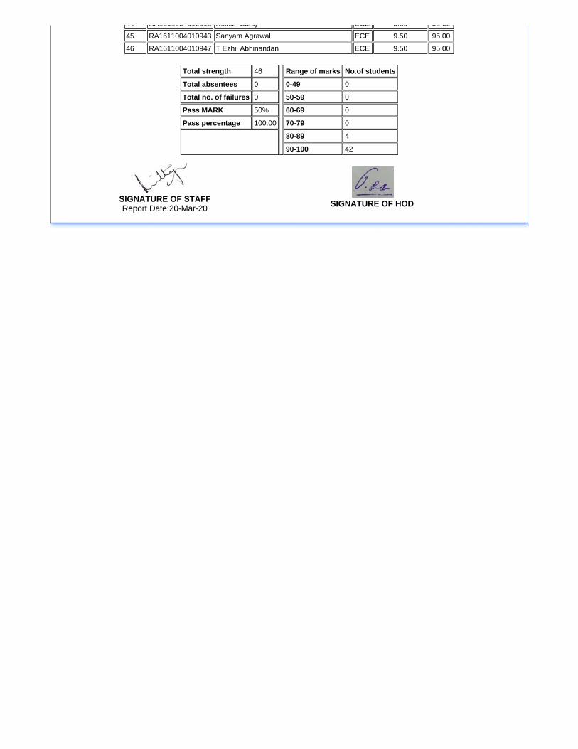
++ ��#*##""+"#"$#2 '��������: ��� $12" $21""
+2 ��#*##""+"#"$+, �����0�����9�� ��� $12" $21""
+* ��#*##""+"#"$+3 ���=����)������� ��� $12" $21""
����8��#� 4�/ +* �� 4��9��#$� ��"�9��:6� ��
����8�5�� ���� " &;'( "
����8 �"�99��8:#�� " �&;�( "
�������< 2"> )&;)( "
������#,� ��4� #""1"" =&;=( "
>&;>( +
(&;%&& +!
3� �������3������; �����?!"%���%!"
3� ���������

���������� ������� ��������� �
���������� ������������������ � ���������������
���������� ����!"#$�%�!"!"�%��&�'(
���������
�����������������
����� � ���!"��#$�%�"&&��#$�
%���'()�*��+�#�#�+�,�-���������)���#"."���/0�*%&&12'-
3"��" ��4"�� ���� ���� 5��� �6��#$ 7
# ��#*##""+"#"",- ���������&�.�.����/�0��� ��� #+1"" $,1,,
! ��#*##""+"#""�- . ����������&�������������������� ��� #�1"" #""1""
, ��#*##""+"#""-+ 4 �������5�����6����7 ��� #+1"" $,1,,
+ ��#*##""+"#"##" . ������������ ��� #+1"" $,1,,
� ��#*##""+"#"##! .����4����� ��� #+1"" $,1,,
* ��#*##""+"#"#,+ ���&������������������� ��� #�1"" #""1""
� ��#*##""+"#"#,$ ���������� ��� #+1"" $,1,,
- ��#*##""+"#"#$� ������5�80����������� ��� #+1"" $,1,,
$ ��#*##""+"#"!#" .�����0� ��9��������������� ��� #+1"" $,1,,
#" ��#*##""+"#"!,+ �������������� ��� #+1"" $,1,,
## ��#*##""+"#"!,- ��7�������� ��� #�1"" #""1""
#! ��#*##""+"#"!�- .�������.��0���0�� ��� #�1"" #""1""
#, ��#*##""+"#"!-, ������������������ ��� #�1"" #""1""
#+ ��#*##""+"#"!$" . ����������� ��� #�1"" #""1""
#� ��#*##""+"#",#+ �����0���� : ��� #�1"" #""1""
#* ��#*##""+"#",!! �������������� ��� #+1"" $,1,,
#� ��#*##""+"#",,- 6����; ��� #�1"" #""1""
#- ��#*##""+"#",�� ���0������7���������� ��� #+1"" $,1,,
#$ ��#*##""+"#",�� ���7�;���������;�������� ��� #�1"" #""1""
!" ��#*##""+"#",-! ����������� ���9����&��0� ��� #�1"" #""1""
!# ��#*##""+"#",-* '�������0�'���������� ��� #�1"" #""1""
!! ��#*##""+"#",$# ������0���7���5�����&��0� ��� #+1"" $,1,,
!, ��#*##""+"#",$+ �������)���4���� ��� #�1"" #""1""
!+ ��#*##""+"#"+,� .������/0�)��� ��� #�1"" #""1""
!� ��#*##""+"#"+�$ �)����������� ��� #�1"" #""1""
!* ��#*##""+"#"+** ������4���� ;������ ��� #�1"" #""1""
!� ��#*##""+"#"+�- . ��� �/�����7������������ ��� #�1"" #""1""
!- ��#*##""+"#"+-, ����� ��� #�1"" #""1""
!$ ��#*##""+"#"+$+ ����������&��� ��� #�1"" #""1""
," ��#*##""+"#"�"! .�))��� ���9��� ��� #�1"" #""1""
,# ��#*##""+"#"��- ����9���6����� ��� #�1"" #""1""
,! ��#*##""+"#"�*! 5�������'����������0�� ��� #�1"" #""1""
,, ��#*##""+"#"�*, ��� �9��4�������:�� ��� #�1"" #""1""
,+ ��#*##""+"#"�** �)������.���� ��� #�1"" #""1""
,� ��#*##""+"#"��� ��0 �����������) �� ��� #�1"" #""1""
,* ��#*##""+"#"�$+ ������� �� ��� #�1"" #""1""
,� ��#*##""+"#"*,- ���0�����9���������� ��� #�1"" #""1""
,- ��#*##""+"#"*+� ���7���4��7�� ��� #�1"" #""1""
,$ ��#*##""+"#"**! �)���)������<�;� ��� #�1"" #""1""
+" ��#*##""+"#"�"� &���&7�� ��� #�1"" #""1""
+# ��#*##""+"#"�+* � �����<������ ��� #�1"" #""1""
+! ��#*##""+"#"��� ���7�:� �<� �� ��� #�1"" #""1""
+, ��#*##""+"#"�$� ��������;�� ���� ��� #�1"" #""1""
++ ��#*##""+"#"$#� '��� ����: ��� #�1"" #""1""
Eswaran
Highlight
Eswaran
Highlight

++ ��#*##""+"#"$#� '��������: ��� #�1"" #""1""
+� ��#*##""+"#"$+, �����0�����9�� ��� #�1"" #""1""
+* ��#*##""+"#"$+� ���=����)������� ��� #�1"" #""1""
����8��#� 4�/ +* �� 4��9��#$� ��"�9��:6� ��
����8�5�� ���� " &;'( "
����8 �"�99��8:#�� " �&;�( "
�������< �"> )&;)( "
������#,� ��4� #""1"" =&;=( "
>&;>( "
(&;%&& +*
3� �������3������; �����?!"%���%!"
3� ���������

���������� ������� ��������� �
���������� ������������������ � ���������������
���������� ����!"#$�%�!"!"�%��&�'(
���������
������������������
����� � ���!"��#$��&"&&��#$�
�������������#�#�������������)���#"�"���� ���&&�2�
3"��" ��4"�� ���� ���� 5��� �6��#$ 7
# ��#*##""+"#"",- ���������&�.�.����/�0��� ��� #$1," $*12"
! ��#*##""+"#""3- . ����������&�������������������� ��� #$1!" $*1""
, ��#*##""+"#""-+ 4 �������5�����6����7 ��� #$1$" $$12"
+ ��#*##""+"#"##" . ������������ ��� #$1!" $*1""
2 ��#*##""+"#"##! .����4����� ��� #$1$" $$12"
* ��#*##""+"#"#,+ ���&������������������� ��� #$1," $*12"
3 ��#*##""+"#"#,$ ���������� ��� #$12" $312"
- ��#*##""+"#"#$2 ������5�80����������� ��� #$1!" $*1""
$ ��#*##""+"#"!#" .�����0� ��9��������������� ��� #$1#" $212"
#" ��#*##""+"#"!,+ �������������� ��� #$12" $312"
## ��#*##""+"#"!,- ��7�������� ��� #$13" $-12"
#! ��#*##""+"#"!2- .�������.��0���0�� ��� #$1," $*12"
#, ��#*##""+"#"!-, ������������������ ��� #$1+" $31""
#+ ��#*##""+"#"!$" . ����������� ��� #$13" $-12"
#2 ��#*##""+"#",#+ �����0���� : ��� #$1+" $31""
#* ��#*##""+"#",!! �������������� ��� #$12" $312"
#3 ��#*##""+"#",,- 6����; ��� #$12" $312"
#- ��#*##""+"#",22 ���0������7���������� ��� #$1!" $*1""
#$ ��#*##""+"#",32 ���7�;���������;�������� ��� #$1!" $*1""
!" ��#*##""+"#",-! ����������� ���9����&��0� ��� #$1+" $31""
!# ��#*##""+"#",-* '�������0�'���������� ��� #$1," $*12"
!! ��#*##""+"#",$# ������0���7���5�����&��0� ��� #$12" $312"
!, ��#*##""+"#",$+ �������)���4���� ��� #$1+" $31""
!+ ��#*##""+"#"+,2 .������/0�)��� ��� #$13" $-12"
!2 ��#*##""+"#"+2$ �)����������� ��� #$1-" $$1""
!* ��#*##""+"#"+** ������4���� ;������ ��� #$13" $-12"
!3 ��#*##""+"#"+3- . ��� �/�����7������������ ��� #$13" $-12"
!- ��#*##""+"#"+-, ����� ��� #$1$" $$12"
!$ ��#*##""+"#"+$+ ����������&��� ��� #$1+" $31""
," ��#*##""+"#"2"! .�))��� ���9��� ��� #$1#" $212"
,# ��#*##""+"#"22- ����9���6����� ��� #$13" $-12"
,! ��#*##""+"#"2*! 5�������'����������0�� ��� #$1," $*12"
,, ��#*##""+"#"2*, ��� �9��4�������:�� ��� #$1-" $$1""
,+ ��#*##""+"#"2** �)������.���� ��� #$13" $-12"
,2 ��#*##""+"#"232 ��0 �����������) �� ��� #$1!" $*1""
,* ��#*##""+"#"2$+ ������� �� ��� #$1-" $$1""
,3 ��#*##""+"#"*,- ���0�����9���������� ��� #$1#" $212"
,- ��#*##""+"#"*+3 ���7���4��7�� ��� #$12" $312"
,$ ��#*##""+"#"**! �)���)������<�;� ��� #$1!" $*1""
+" ��#*##""+"#"3"3 &���&7�� ��� #$12" $312"
+# ��#*##""+"#"3+* � �����<������ ��� #$1!" $*1""
+! ��#*##""+"#"322 ���7�:� �<� �� ��� #-1#" $"12"
+, ��#*##""+"#"3$2 ��������;�� ���� ��� #-1#" $"12"
++ ��#*##""+"#"$#2 '��� ����: ��� #$12" $312"
Eswaran
Highlight
Eswaran
Highlight

++ ��#*##""+"#"$#2 '��������: ��� #$12" $312"
+2 ��#*##""+"#"$+, �����0�����9�� ��� #$1+" $31""
+* ��#*##""+"#"$+3 ���=����)������� ��� #$1+" $31""
����8��#� 4�� +* �� 4��9��#$� ��"�9��:6� ��
����8�5�� ���� " &;�� "
����8 �"�99��8:#�� " �&;�� "
�������< 2"> �&;�� "
������#� ��4� #""1"" =&;=� "
>&;>� "
�&;�&& +*
3� �������3������; �����?"+%6��%!"
3� ���������

PROJECT REPORT – 1
7. Certificate by HoD