
Project 4H Hardware Specification - Digi...
51
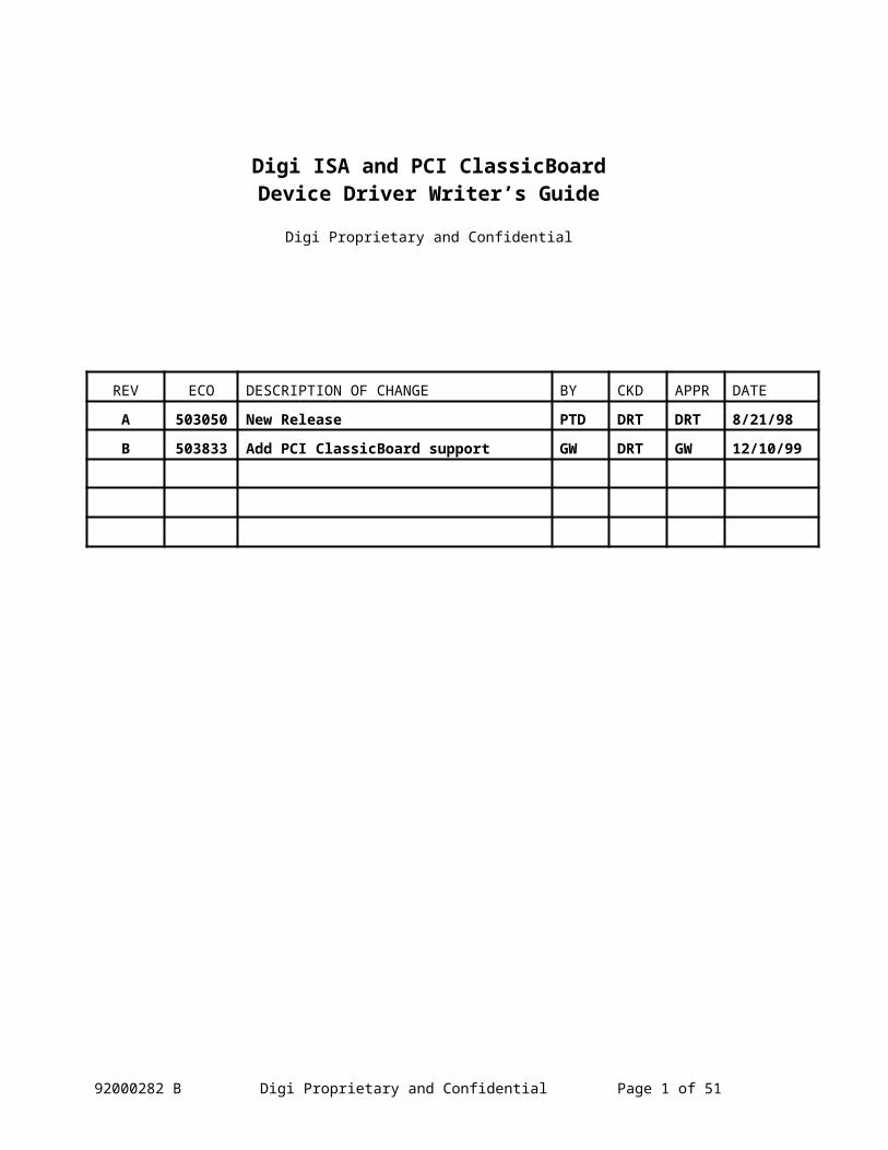
Digi ISA and PCI ClassicBoard Device Driver Writer’s Guide Digi Proprietary and Confidential REV ECO DESCRIPTION OF CHANGE BY CKD APPR DATE A 503050 New Release PTD DRT DRT 8/21/98 B 503833 Add PCI ClassicBoard support GW DRT GW 12/10/99 92000282 B Digi Proprietary and Confidential Page 1 of 51
Transcript of Project 4H Hardware Specification - Digi...
Digi ISA and PCI ClassicBoardDevice Driver Writer’s Guide
Digi Proprietary and Confidential
REV ECO DESCRIPTION OF CHANGE BY CKD APPR DATE
A 503050 New Release PTD DRT DRT 8/21/98
B 503833 Add PCI ClassicBoard support GW DRT GW 12/10/99
92000282 B Digi Proprietary and Confidential Page 1 of 39
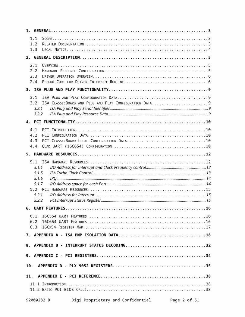
1. GENERAL................................................................................................................................................. 3
1.1 SCOPE................................................................................................................................................... 31.2 RELATED DOCUMENTATION.................................................................................................................. 31.3 LEGAL NOTICE...................................................................................................................................... 4
2. GENERAL DESCRIPTION...................................................................................................................... 5
2.1 OVERVIEW............................................................................................................................................ 52.2 HARDWARE RESOURCE CONFIGURATION...............................................................................................52.3 DRIVER OPERATION OVERVIEW............................................................................................................. 62.4 PSEUDO CODE FOR DRIVER INTERRUPT ROUTINE...................................................................................6
3. ISA PLUG AND PLAY FUNCTIONALITY............................................................................................9
3.1 ISA PLUG AND PLAY CONFIGURATION DATA........................................................................................93.2 ISA CLASSICBOARD AND PLUG AND PLAY CONFIGURATION DATA........................................................9
3.2.1 ISA Plug and Play Serial Identifier...............................................................................................93.2.2 ISA Plug and Play Resource Data.................................................................................................9
4. PCI FUNCTIONALITY.......................................................................................................................... 10
4.1 PCI INTRODUCTION............................................................................................................................. 104.2 PCI CONFIGURATION DATA................................................................................................................. 104.3 PCI CLASSICBOARD LOCAL CONFIGURATION DATA............................................................................104.4 QUAD UART (16C654) CONFIGURATION............................................................................................10
5. HARDWARE RESOURCES................................................................................................................... 12
5.1 ISA HARDWARE RESOURCES...............................................................................................................125.1.1 I/O Address for Interrupt and Clock Frequency control..............................................................125.1.5 ISA Turbo Clock Control............................................................................................................135.1.6 IRQ............................................................................................................................................. 145.1.7 I/O Address space for each Port.................................................................................................14
5.2 PCI HARDWARE RESOURCES............................................................................................................... 155.2.1 I/O Address for Interrupt............................................................................................................ 155.2.2 PCI Interrupt Status Register......................................................................................................15
6. UART FEATURES.................................................................................................................................. 16
6.1 16C554 UART FEATURES................................................................................................................... 166.2 16C654 UART FEATURES................................................................................................................... 166.3 16CX54 REGISTER MAP...................................................................................................................... 17
7. APPENDIX A - ISA PNP ISOLATION DATA.......................................................................................18
8. APPENDIX B - INTERRUPT STATUS DECODING............................................................................32
9. APPENDIX C - PCI REGISTERS.......................................................................................................... 34
10. APPENDIX D - PLX 9052 REGISTERS.............................................................................................35
11. APPENDIX E - PCI REFERENCE.....................................................................................................38
11.1 INTRODUCTION.................................................................................................................................... 3811.2 BASIC PCI BIOS CALLS...................................................................................................................... 38
92000282 B Digi Proprietary and Confidential Page 2 of 39

1. General
1.1 Scope
This document is a guide for writing a device driver for the Digi ClassicBoard adapter cards. It is aimed at a user who is either writing a new device driver, or converting an existing PC/X, Multi-Port, Optum or Plus 8 device driver to use a ClassicBoard adapter. This document applies to the ISA or PCI ClassicBoard in these flavors:
4/8 Port EIA-232 adapter with 16C554 UARTs or with 16C654 UARTs 4/8 Port RS422 adapter with 16C554 UARTs or with 16C654 UARTs 4/8 Port RS422 adapter with 16C654 UARTs 16 Port EIA-232 ISA adapter and module with 16C554 or 16C654 UARTs
The hardware resources that the ClassicBoard adapter uses are completely configured by software. The PCI ClassicBoard configuration is performed by the PCI BIOS and O/S. ISA ClassicBoard adapter configuration depends on the O/S. In a Plug and Play O/S this configuration is performed by the O/S, while in a non-Plug and Play (or Legacy) O/S, the configuration can performed by Digi’s Configuration Utility or may be performed by the driver. The primary focus of this document is not how to configure the ClassicBoard (although the appendices supply sufficient information to do this) but how to write a driver for an adapter which is already configured. As such this document is equally applicable whether the ClassicBoard is a PCI or ISA card operating in Plug and Play mode or Legacy mode.
It is assumed the reader is familiar with:
Issues involved in writing device drivers, in particular how to write a device driver for a UART based non-intelligent serial device.
The 16C554 and 16C654 Quad UARTs. The ISA Plug and Play interface, if the driver configures the adapter’s resources. The PCI Local Bus specification. The PCI BIOS and methods of finding the adapter’s resources.
1.2 Related Documentation
ISA Plug and Play Specification, Rev 1.0A and Clarification (http://www.microsoft.com/hwdev/respec/pnpspecs.htm )
Exar (Startech) 16c554, 16c654 UART Data Sheets (http://www.exar.com/products/star/uarts.htm)
PCI Local Bus Specification, Rev. 2.1(http://www.pcisig.com/)
PCI BIOS Specification Digi ISA ClassicBoard Engineering Specifications Digi PCI ClassicBoard Engineering Specifications Digi PC/X, MultiPort, Optum and Plus 8 Engineering Specifications
Other Recommended Reference Material
Plug And Play System Architecture, by Tom Shanley, Mindshare Inc, Addison-Wesley Publishing Co, 1995
ISA System Architecture, by Shanley/Anderson, Mindshare Inc, Addison-Wesley Publishing Co, 1995
1.3 Legal Notice92000282 B Digi Proprietary and Confidential Page 3 of 39

Proprietary Rights NoticeDigi, Digi International, the Digi logo, and ClassicBoard are trademarks or registered trademarks of Digi International Inc. in the United States and other countries. All other brand and product names are trademarks or registered trademarks of their respective holders.This manual is copyrighted material proprietary to Digi International Inc. Copying of this manual without the express written consent of Digi International Inc. is prohibited and will be treated as copyright infringement.Copyright 1999 Digi International Inc. All Rights Reserved. http://www.digi.com
DisclaimerThis manual may contain inaccurate or erroneous information. This manual is subject to change at any time. This manual, including all information contained herein, is provided “as is” without warranty of any kind, either expressed or implied, including but not limited to, any implied warrantees of merchantability of fitness for particular purpose. Digi International Inc. makes no representations, warranties, or commitments with regard to any data or information contained in this manual. If you rely on data or information contained in this manual, such reliance is at your own risk.The Digi logo and ClassicBoard are registered trademarks of Digi International. All other brand and product names are trademarks of their respective holders.
Copyright 1999 Digi International Inc. All Rights Reserved.
92000282 B Digi Proprietary and Confidential Page 4 of 39

2. General Description
2.1 Overview
The Digi ClassicBoard Plug and Play (PnP) ISA adapter card and Digi ClassicBoard PCI adapter card are asynchronous communications cards. They are available in 4, 8 and 16 port versions and are populated with either 16C554 or 16C654 Quad UARTs. Both EIA-232 and EIA-422 versions exist; for currently available models, please refer to the Digi website http://www.digi.com. For brevity, all references to UARTs will mean 16C654's unless otherwise noted.
The ISA adapter has the ability to operate in PnP mode or in ‘legacy’ mode (for those systems that do not support the PnP protocol).
There are no on-board jumpers or DIP switches on the 232 or 422 mode cards. When the ISA adapter is programmed to operate in PnP mode the adapter is configured as per the Plug and Play standards. When the adapter is programmed to operate in ‘Legacy’ mode all the configuration settings are stored in EEPROM.
All PCI adapters are programmed on PCI reset by the PCI BIOS and the configuration settings are stored in an onboard EEPROM. The PCI adapters have no on-board jumpers or DIP switches on the 232 or 422 modes card.
The ISA ClassicBoard adapter is designed to replace all Digi non-intelligent 4, 8 and 16 port RS-232 serial cards and 4 and 8 port RS-422 serial cards. To maintain compatibility with existing drivers, the IRQ status register locations can be configured to operate in a ‘Digi’, ‘Arnet’ or ‘StarGate’ format. In addition, the adapter supports the ability to set the first communications port as a standard COM port. The ISA ClassicBoard adapter replaces the following adapters:
The DigiBoard PC/4, PC/8 and PC/16 cards. The Arnet Multiport 4 and 8 port cards. The StarGate Plus 8 and Optum cards.
2.2 Hardware Resource Configuration
The ISA ClassicBoard fully conforms with the Plug and Play Rev 1.0A specification. Thus, when the ClassicBoard is used in PnP systems, the PnP entity will configure the ClassicBoard to use appropriate hardware resources. How the PnP entity conveys the hardware resources that have been assigned is system dependent. For instance, in the case of Windows 95 this information is available to drivers from the Registry database. It is not in the scope of this document to discuss how to program an ISA PnP configuration utility. Please refer to Section 1.2 for references for more information on that subject.
On Legacy systems the driver writer has two options: Use Digi's DOS-based Configuration Utility, or a similar third-party configurator to configure the resources. Incorporate the Legacy configuration into the driver.
The Digi Configuration Utility is freely available with the adapter and from Digi's Web and FTP sites. This utility uses PnP methodology to configure the adapter and once configured writes these legacy values to EEPROM. If you wish to incorporate the Legacy configuration into your driver, access to the source code for the Configuration Utility may be negotiated. Please contact Digi for further details.
The PCI ClassicBoard fully conforms with the PCI Specification Rev 2.1. When used with a PCI bus meeting the same specification, the PCI BIOS will configure the ClassicBoard to use appropriate hardware resources. How the driver writer obtains the hardware resources is system dependent and is not in the scope of this document however a brief overview is supplied in Appendix E. Please refer to section 1.2 for references for more information on that subject.
92000282 B Digi Proprietary and Confidential Page 5 of 39
2.3 Driver Operation Overview
A standard non-intelligent COM port has an 8 byte I/O address space to control the port’s UART and will typically have an interrupt dedicated to that port. The 8-byte I/O address space addresses the 8 registers on the UART. The corresponding registers are described in the UART Data Sheets. The ISR register on board the UART determines what interrupt, if any, is pending and the reason the UART is interrupting. Thus, when a standard COM port interrupt occurs, the driver examines the ISR and takes the appropriate action to resolve the interrupt, which in turn causes the interrupt to cease.
From a driver writer viewpoint, a ClassicBoard adapter can be considered as many standard non-intelligent COM ports which share the same interrupt. Since an interrupt is shared among many COM ports there is another I/O address space, common to all ports on the same ClassicBoard adapter, which facilitates deciphering the port or ports responsible for the interrupt. The driver could simply poll the ISR of all ports that share the same interrupt when an interrupt occurs, but this is less efficient.
The PCI ClassicBoard provides two registers to help determine which port generated an interrupt. The PLX Interrupt Control/Status register tells which UART (in the case of 8 port systems) caused the interrupt while the ClassicBoard’s Interrupt status register defines which port generated the interrupt.
The ISA boards provide various methods for determining which port generated the interrupt. The ISA ClassicBoard supports three Interrupt Modes, including DigiBoard, StarGate and Arnet. There is no particular advantage to using one mode over another, other than the Arnet mode is restricted to work with a maximum of 8 ports. Please remember that the Digi ClassicBoards do NOT support interrupt daisy-chaining between boards, as the DigiBoard PC/8 did.
On the ISA ClassicBoard the register at this address also determines the clock frequency driving the Quad UARTs, it is called the Interrupt/Clock status register. The power-on default UART clock setting is a frequency of 1.8432 MHz, which can be increased to 7.3728 MHz by writing to the Interrupt/Clock status register. This has the effect of quadrupling the Baud rate, and the maximum Baud rate will be 460.8K instead of 115.2K Baud. The PCI ClassicBoard has a standard UART clock of 7.3728 MHz.
Port 1 on the ISA ClassicBoard is a special port, able to be configured (either by PnP or the legacy Configuration Program) to emulate a standard non-intelligent COM port. When set as a stand-alone COM port, it uses a dedicated interrupt and the Interrupt/Clock status register will not indicate when an interrupt is pending for Port 1. The clock frequency is still controlled by the Interrupt/Clock status register and will use the same clock frequency as Ports 2, 3 and 4. This is because Port 1 is still the first UART of the first Quad UART and all four UARTs on a given Quad UART will share the same clock.
Port 2 on the 4 and 8 port ISA ClassicBoard is another exception. The DigiBoard PC/4 and PC/8, which the ClassicBoard replaces, allows port 2 to be configured with its own interrupt. For backward compatibility this functionality is available on 4 and 8 port ClassicBoards. Generally, on most systems interrupts are at a premium and one interrupt will be shared by all ports.
Typically, there is no performance gain in having separate interrupts for Ports 1 and 2. These ports are usually only allocated separate interrupts in order to support existing applications.
2.4 Pseudo Code for Driver Interrupt Routine
The following Pseudo Code is a typical sample of how to implement the interrupt procedure for the ISA ClassicBoard adapter in DigiBoard Interrupt Mode or a PCI ClassicBoard. In this case Port 1 is configured to share interrupts with the other ports.
// determine port requesting serviceread port = Interrupt/Clock Status Registerif (no port requires service)
returndo
read ISR of port92000282 B Digi Proprietary and Confidential Page 6 of 39
Sandy, 01/03/-1,
This section might read better if it were split into a ISA adapter section and a PCI adapter section.

service interrupt based on ISR// See if there is another port requesting serviceread port = Interrupt/Clock Status Register
while ( port requests service)return
92000282 B Digi Proprietary and Confidential Page 7 of 39

The following Pseudo Code is a typical sample of how to implement the interrupt procedure for the ClassicBoard adapter in StarGate or Arnet Interrupt Mode. In this case, Port 1 is configured to share interrupts with the other ports.
// determine ports requesting serviceread portMask = Interrupt/Clock Status Registermask the first port (port) requesting service from portMask variableif (no port requires service)
returndo
doread ISR of portservice interrupt based on ISRmask the next port (port) requesting service from portMask variable
while (port)// determine if another port is requesting serviceread portMask = Interrupt/Clock Status Registermask the first port (port) requesting service from portMask variable
while (port)return
92000282 B Digi Proprietary and Confidential Page 8 of 39

3. ISA Plug and Play Functionality
3.1 ISA Plug and Play Configuration Data
As per the ISA Plug and Play specification, the ISA ClassicBoard adapter will respond to reads from the Serial Isolation register by returning the adapter’s serialized configuration information. The serialized data is returned in two formats, the Serial Identifier data and the Resource data. The general format of the Resource data can be further broken down into: Plug and Play version number type. Identifier string resource type. One or more logical device ID resource types. End tag resource type to indicate the end of resources for this Plug and Play card.
3.2 ISA ClassicBoard and Plug and Play Configuration Data
During the Plug and Play Isolation sequence the Digi ISA ClassicBoard returns the Serial Identifier data and Resource data consisting of up to six Logical Devices.
Table 3.1 summarizes the Functionality of each Logical Device.
Table 3.1 ClassicBoard PnP Logical Devices
Logical Device #
Present On IRQs Allocated
I/0s Allocated
Functionality
0 4, 8 and 16 port adapters 1 1x8 bytes Adapter’s IRQ and UART Clock Frequency selection
1 4, 8 and 16 port adapters 1 (Optional)
1x8 bytes Control of Port 1 on the1st Quad UART
2 4, 8 and 16 port adapters None(Note 1)
3x8 bytes Control of Ports 2 - 4 on the 1st Quad UART
3 8 and 16 port adapters None 4x8 bytes Control of 2nd Quad UART (Ports 5 - 8)
4 16 port adapters None 4x8 bytes Control of 3rd Quad UART (Ports 9 - 12)
5 16 port adapters None 4x8 bytes Control of 4th Quad UART (Ports 13 - 16)
Note 1: ClassicBoard 4 and 8 port adapters may optionally allocate a separate IRQ for Port 2.
3.2.1 ISA Plug and Play Serial Identifier
Appendix A1 defines the Serial Identifier returned by ISA ClassicBoard adapters.
3.2.2 ISA Plug and Play Resource Data
Appendices A2 - A10 define the Resource Data that the ISA ClassicBoard adapter returns. Logical Device #3 is only returned by 8 and 16 port adapters. Logical Devices #4 & #5 are only returned by 16 port adapters.
92000282 B Digi Proprietary and Confidential Page 9 of 39

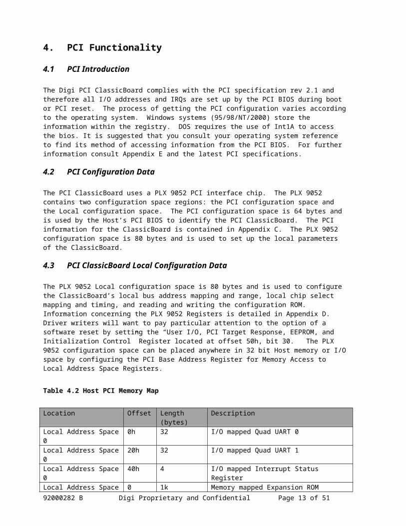
4. PCI Functionality
4.1 PCI Introduction
The Digi PCI ClassicBoard complies with the PCI specification rev 2.1 and therefore all I/O addresses and IRQs are set up by the PCI BIOS during boot or PCI reset. The process of getting the PCI configuration varies according to the operating system. Windows systems (95/98/NT/2000) store the information within the registry. DOS requires the use of Int1A to access the bios. It is suggested that you consult your operating system reference to find its method of accessing information from the PCI BIOS. For further information consult Appendix E and the latest PCI specifications.
4.2 PCI Configuration Data
The PCI ClassicBoard uses a PLX 9052 PCI interface chip. The PLX 9052 contains two configuration space regions: the PCI configuration space and the Local configuration space. The PCI configuration space is 64 bytes and is used by the Host’s PCI BIOS to identify the PCI ClassicBoard. The PCI information for the ClassicBoard is contained in Appendix C. The PLX 9052 configuration space is 80 bytes and is used to set up the local parameters of the ClassicBoard.
4.3 PCI ClassicBoard Local Configuration Data
The PLX 9052 Local configuration space is 80 bytes and is used to configure the ClassicBoard’s local bus address mapping and range, local chip select mapping and timing, and reading and writing the configuration ROM. Information concerning the PLX 9052 Registers is detailed in Appendix D. Driver writers will want to pay particular attention to the option of a software reset by setting the “User I/O, PCI Target Response, EEPROM, and Initialization Control” Register located at offset 50h, bit 30. The PLX 9052 configuration space can be placed anywhere in 32 bit Host memory or I/O space by configuring the PCI Base Address Register for Memory Access to Local Address Space Registers.
Table 4.2 Host PCI Memory Map
Location Offset Length (bytes) Description
Local Address Space 0 0h 32 I/O mapped Quad UART 0Local Address Space 0 20h 32 I/O mapped Quad UART 1Local Address Space 0 40h 4 I/O mapped Interrupt Status RegisterLocal Address Space 1 0 1k Memory mapped Expansion ROM (optional)Local Address Space 2 0 32 Memory mapped Quad UART 0Local Address Space 2 20h 32 Memory mapped Quad UART 1Local Address Space 2 40h 4 Memory mapped Interrupt Status registerLocal Configuration Space 0 80 Local Configuration Registers
4.4 Quad UART (16C654) Configuration
The Quad UARTs and the Interrupt Status Register can be accessed in both PCI Memory and I/O space. Local address space 0 (32 bit I/O mapped) and local address space 2 (32 bit memory mapped) are used to access both data and control register in the two quad UARTs. Both Quad UARTs are selected by PLX 9052 local chip select 0 and are mapped in to local memory space base address 0 (see Appendix D.) The PCI Host addressing for local memory space 0 is on byte boundaries and the range is 64 bytes.
Local address space 0 and local address space 2 also are used to read the UART interrupt status register. This read only register is decoded by PLX 9052 local chip select 2 and returns a byte which represents the current state of each of the eight UART interrupts. Each UART interrupt is mapped into a bit of the byte: UART 0’s
92000282 B Digi Proprietary and Confidential Page 10 of 39

interrupt in reflected in bit 0; UART 7’s interrupt is bit 7. An active UART interrupt returns a “1” when the interrupt status register is read.
The local address space 1 is used to access the optional expansion ROM (used for Vendor Product Data) which is mapped into upper local address space on byte address boundaries and is decoded by the PLX 9052 local chip select 1. The current ROM range is 1 K Bytes max. The expansion ROM offered on standard PCI ClassicBoards is not currently used so none of the associated functions need to be implemented.
92000282 B Digi Proprietary and Confidential Page 11 of 39

5. Hardware Resources
5.1 ISA Hardware Resources
After the ISA Plug and Play entity has enumerated the Logical Devices on the ClassicBoard the following resources will be reserved for the ISA ClassicBoard :
An 8-byte block of I/O address space, used for control of the adapter’s shared IRQ as well as Quad UART clock frequency selection.
At least one IRQ, possibly 2 (ISA only.) An 8-byte block of I/O address space for each available Port. (4x8-byte I/O address spaces for each
available Quad UART.)
How the ISA Plug and Play or PCI BIOS entity communicates the values of the resources reserved will be a function of the implementation of the respective entity for your system and is beyond the scope of this document. In the case of Windows 95 the entity stores this information in the Registry database.
Under Legacy Mode, the ISA ClassicBoard will require the same resources, however, the board is first configured using Digi's Configuration Utility. The Legacy Driver is subsequently configured by the user to match these configuration settings. Thus, the following discussion is applicable to adapters in Legacy as well as PnP mode.
5.1.1 I/O Address for Interrupt and Clock Frequency control
An 8-byte I/O address space is used to control the ISA card’s Interrupt and the Clock Frequency of each Quad UART. In Plug and Play mode this I/O address space corresponds to the I/O address space which Logical Device #0 reserves. (In Legacy mode, this address space should be configured using the DOS Digi Configuration Utility.)
Table 5.1 depicts the register alignment of Interrupt and Clock Frequency control I/O address space.
Table 5.3 – Interrupt and Clock Frequency Control I/O Address Space
Location Register Name R/W Functionality00 IRQ Status Register A R Reports status for ports 1-8
(DigiBoard and StarGate modes)
01 IRQ Status Register B R Reports status for ports 9 - 16 (StarGate mode)Reports a mirror-image of location 00 (DigiBoard mode)
02 IRQ Status Register C R Reports status for ports 1-8 (Arnet mode)
03 IRQ Status Control Register
R/W Selects status register mode
04 TCLK Control Register R/W Selects UART clock frequency05 Reserved - Not utilized06 Reserved - Not utilized07 Reserved - Not utilized
Locations 00 - 02 are Read-only locations, whose interpretation is dependent upon the Interrupt Mode selected. (DigiBoard, Arnet, StarGate and Disabled.) DigiBoard Interrupt Mode is the factory default setting in PnP ISA mode. The ClassicBoard PCI does not have compatibility modes like the ISA card; it uses a bitmap of each port requiring service (similar to the Stargate mode). Only one byte of status is supported.
92000282 B Digi Proprietary and Confidential Page 12 of 39
Location 03, the IRQ Status Control Register, is a R/W location that determines the Interrupt Mode. A hexadecimal mask of 0xA0 is used when setting the Interrupt Mode. This mask is not used when reading the Interrupt Mode setting. The Write and Read values are defined in Table 5.2.
Table 5.4 - IRQ Status Control Register Values
Interrupt Mode Write Value (Hex)
Read Value (Hex)
DigiBoard 0xA0 0x00Arnet 0xA1 0x01
StarGate 0xA2 0x02Disable Interrupts 0xA3 0x03
In DigiBoard mode, locations 0 or 1 are used. In StarGate mode, locations 0 - 1 are used. In Arnet mode, location 2 is used. When Interrupts are disabled Locations 0 - 2 report 0xFF.
While there is no particular advantage in using one mode over another, the three modes allow backward compatibility for existing legacy drivers. The Interrupt Mode can be altered by the software driver in PnP and legacy ISA systems, or by the Digi Configuration Utility in legacy ISA systems.
5.1.1.1 DigiBoard Mode
In DigiBoard Mode, which is the default power up mode in PnP, the ports that require attention are successively indicated in location 0 and 1. (These locations are mirror images of one other, and are required for backward compatibility.) Since only one port is indicated at a time, the status location must be successively read to determine all the ports that have interrupts pending. Only when the a port’s interrupt is satisfied will the interrupt from that port cease, and only then will the next port number requiring attention be available in the Status Control Register.
These locations report 0xFF when no interrupts are pending. For more information refer to the tables in Appendix B.
5.1.1.2 StarGate Mode
In StarGate Mode, Locations 0 - 1 indicate the ports that require attention. Since a bit-mask is used, a single read of Locations 0 - 1 may indicate more than one port has a pending interrupt. When no port requires attention, Location 0 - 1 reads 00. For more information refer to the tables in Appendix B.
5.1.1.3 Arnet ModeIn Arnet Mode, Location 2 indicates the ports that require attention. Since a bit-mask is used, a single read of Locations 2 may indicate more than one port has interrupts pending. When no port requires attention, Location 2 reads 0xFF Hexadecimal. For more information refer to the tables in Appendix B.
NOTE: Since this register location is bit-mapped, Arnet mode is capable of supporting a maximum of 8 ports.
5.1.1 ISA Turbo Clock Control
Location 04, the Turbo Clock Control register, is used to control the clock frequency fed to the UARTs. The frequency output for each UART is switchable between 1.8432 MHz (logical 0) and 7.3728 MHz (logical 1) through the use of this register location. The register defaults to 0x00 (1.8432 MHz clocks to all UARTs) upon power up. A hexadecimal mask of 0xA0 is used when setting the Turbo Clock Control. This mask is not used when reading the setting. Table 3 defines the setting for enabling the Turbo Clock (7.3728 MHz) and the values read when the Turbo Clock is enabled.
92000282 B Digi Proprietary and Confidential Page 13 of 39

Table 5.4 – Turbo Clock Control Register Values
Enable Turbo Location 4 Write Values Location 4 Read ValuesClock on: MSB LSB MSB LSB
7 6 5 4 3 2 1 0 7 6 5 4 3 2 1 0Quad UART #1 1 0 1 0 x x x 1 0 0 0 0 x x x 1Quad UART #2 1 0 1 0 x x 1 x 0 0 0 0 x x 1 xQuad UART #3 1 0 1 0 X 1 x x 0 0 0 0 x 1 x xQuad UART #4 1 0 1 0 1 x x x 0 0 0 0 1 x x x
The Turbo Clock is controlled on a Quad UART basis, which means that each of the 4 ports common to the same Quad UART also share the same Turbo Clock setting. In other words, ports 1 - 4 share a clock setting, ports 5 - 8 share a setting, ports 9 - 12 share a setting and ports 13 - 16 share a setting.
Setting the Turbo Clock produces Baud rates which are 4 times greater that the Baud rate when the Turbo Clock is disabled. This Turbo Clock feature will allow a maximum data rate of 460.8K Baud instead of 115.2K Baud. Both 16C554 and 16C654 Quad UART will function correctly with the Turbo Clock enabled. However, since the 16C554 does not allow Flow Control to be handled automatically by the UART, and since its FIFOs are only 16 bytes deep (instead of 64 on the 16C654) your operating system may find it difficult to keep up with ports with 16C554 UARTs operating at data rates above 115.2K Baud. Thus, for many operating systems it is not recommended to operate 16C554 UARTs above 115.2K Baud.
Refer to the Exar 16C554 and 16C654 Data Sheets for further details on Clock speeds and Automatic Flow control.
Locations 05 - 07 are reserved for factory use and should not be used.
5.1.2 IRQ
In Plug and Play ISA mode, at least one IRQ will be reserved for the ClassicBoard. This IRQ is used to indicate when one of the Serial Ports needs servicing. Upon receiving an interrupt, the IRQ Status Control Register may be read to determine the Port that is requesting service. The ISR on the UART in question may then be read and appropriate action taken to service the interrupt.
Typically, only when a port’s interrupt is satisfied will the interrupt from that port cease. Some of the typical ways of satisfying an interrupt from a UART include :
Reading the UARTs Interrupt Service Register (ISR), in the case of transmit interrupts. Reading all available receive characters, in the case of receive interrupts. Masking out the relevant interrupt in the UARTs Interrupt Enable Register (IER).
The first port on the first Quad UART is a special case. This port can be configured on ISA boards to emulate a standard serial port. If this port is configured in this fashion, it uses an IRQ solely dedicated to this port. In this case the IRQ used for the remaining ports will never indicate that the first port requires attention.
5.1.3 I/O Address space for each Port
Each port number has its own 8 byte I/O address space used to control the associated UART. The interpretation of this I/O address space is defined in the Quad UART’s data specification.
When the ISA ClassicBoard is used in Legacy mode, the UARTs will occupy a specific set of addresses that are picked by the user. Digi supplies several default profile files with the Configuration Utility which can be used to configure a ClassicBoard when emulating a legacy board such as a PC/X , Multi-Port, Optum or Plus 8. The user can specify a new set of addresses to use, and save that profile for re-use through the Configuration Utility.
The user should remember that the ISA ClassicBoard can be programmed to use any I/O address, and conflicts with some standard ISA devices may prevent the system from operating. Digi's Configuration Utility will not allow the user to select some addresses in order to prevent such conflicts. An example configuration would be to
92000282 B Digi Proprietary and Confidential Page 14 of 39

program the UARTs to start at address 0x1C0. This will conflict with the IDE controller at 0x1F0, and may cause the system to fail to boot. Other addresses may cause conflicts such that the ClassicBoard cannot be reprogrammed in a PC; the board must then have its EEPROM removed and replaced with a blank EEPROM.
5.2 PCI Hardware Resources
The PCI ClassicBoard does not have a Turbo-Clock mode such as the ISA ClassicBoard. The clock for the UARTs on the PCI ClassicBoard is always 14.7456 MHz. All PCI Classic boards use one IRQ at most and operate in only one mode (as opposed to DigiBoard, Stargate, or Arnet modes.) An 8-byte block of I/O space and Memory space is reserved for each available port and are assigned in sucsession from the Memory or I/O Mapped UARTs and Status base address provided in the PCI registers. Control of PCI fuctions is provided through the PLX Configuration Registers which are located at the address specified in the PCI registers. All I/O space addresses and memory space addresses are determined by the PCI BIOS on PCI reset or system boot.
5.2.1 I/O Address for Interrupt
The PCI Classic Board has interrupt control at several locations. The PLX Configuration Registers provide a master interrupt control/status register at offset 4Ch from the PLX Configuration Registers. This register enables and disables interrupts from each of the possible two UARTs in addition to enabling and disabling the interrupt to the processor.
This register also provides two status bits that show the current interrupt status of each of the UARTs. These bits should be checked in an interrupt service routine to see which UART caused the interrupt.
The interrupt control/status register also provides a software interrupt bit, which is useful for testing. A bitmap of this register is provided in Appendix D.
In additon each port has its Interrupt Status Register within its 8-byte block of I/O space. See the UARTs data sheet for more information.
5.2.2 PCI Interrupt Status Register
The PCI ClassicBoard's Interrupt Status Register will read as a bitmap of each port that requires service. A logical 1 indicates an active interrupt on that port, as shown below. This read-only register supports the maximum of 8 ports for the PCI cards. This register is located at offset 40h from either the I/O or memory base addresses and may be read to detirmine which ports interrupt need servicing.
Table 5.3 - PCI ClassicBoard Interrupt Status Register Map
MSB LSB7 6 5 4 3 2 1 0
Interrupting Port Port 8
Port 7 Port 6 Port 5 Port 4 Port 3 Port 2 Port 1
This register only provides a means to tell which port has caused the interrupt. The driver writer must then service the corresponding port’s interrupt status register in addition to the PLX chip’s Interrupt Control/Status Register. Both of these registers therefor need setting to enable interrupts on a specific port.
Note that the PCI IRQ is a level-sensitive interrupt at all times. This is in contrast to the ISA method of an edge-sensitive interrupt. Because the IRQ is level-sensitive, it is also possible to share PCI interrupts with other devices. The interrupt handler for the PCI ClassicBoard should be written in a manner that accomodates a level-sensitive interrupt and allows for sharing interrupt requests.
92000282 B Digi Proprietary and Confidential Page 15 of 39

6. UART Features
The PCI ClassicBoard adapters are populated with 16c654 Quad UART ICs while the ISA ClassicBoard adapters can be populated with either 16C654 or 16c554 Quad UART ICs. The 4/8 port ISA ClassicBoard adapters distinguish between the two different UART types with the revision field of the Logical Device Resource Data. The 16 port ISA adapter are unable to do this, so the driver must examine the UART registers to determine whether 16C654 or 16C554 UART is present.
One method of detecting the two types of UARTs is to check for the existence of the 16c654's enhanced function register. This routine would only need to be run on one port on the board, since both Quad UARTs will always be of the same type.
// detect the presence of 16c654 UARTs vs. 16c554 UARTsread port = UART Device
set LCR of port = 0xBF //turn on enhanced functionsread ISR of port //the ISR is the EFR in enhanced modeset LCR of port = 0x00 //return to normal mode
if ISR == 0return (port == 16c654)
elsereturn (port == 16c554)
6.1 16C554 UART Features
The 16C554 Quad UART has the following features:
Four independent 16C550 compatible UARTs on one chip. Independent 16 Byte Transmit and 16 Byte Receive FIFOs in each UART. Operation up to 460.8K Baud with Turbo Clock (7.3728 MHz) enabled (ISA version).
6.2 16C654 UART Features
The 16C654 Quad UART has the following features : Four independent enhanced UARTs on one chip. Independent 64 Byte Transmit and 64 Byte Receive FIFOs. Operation up to 460.8K Baud with Turbo Clock (7.3728 MHz) enabled (ISA version). Note that the PCI
version uses a clock of 14.7456 MHz. Automatic handling of Hardware and Software Flow Control by the UART. FIFO trigger levels are different from (deeper than) the 16C554.
92000282 B Digi Proprietary and Confidential Page 16 of 39

6.3 16Cx54 Register Map
The general register map is provided. For more information the register’s contents consult the 16C554 or 16C654 datasheet. A2, A1, and A0 represent the lowest address bits, add these to the Local Address Register 0 (I/O mapped) or Local Address Register 2 (Memory Mapped.) All four UARTs are addressed in succession.
Table 6.5 General Register Set
A2 A1 A0 Read Mode Write Mode0 0 0 Receive Holding Register Transmit Holding Register0 0 1 Interrupt Enable Register0 1 0 Interrupt Status Register FIFO Control Register0 1 1 Line Control Register1 0 0 Modem Control Register1 0 1 Line Status Register1 1 0 Modem Status Register1 1 1 Scratch Pad Register Scratch Pad Register
The Baud Rate Registers may only be accessed when bit-7 of the Line Control Register is set.
Table 6.6 Baud Rate Register Set
A2 A1 A0 Read Mode Write Mode0 0 0 LSB of Divisor Latch LSB of Divisor Latch0 0 1 MSB of Divisor Latch MSB of Divisor Latch
The Enhanced Register Set may only be accessed when the Line Control Register is set to 0xBFh.
Table 6.7 Enhanced Register Set
A2 A1 A0 Read Mode Write Mode0 1 0 Enhanced Feature Register Enhanced Feature Register1 0 0 Xon-1 Word Xon-1 Word1 0 1 Xon-2 Word Xon-2 Word1 1 0 Xoff-1 Word Xoff-1 Word1 1 1 Xoff-2 Word Xoff-2 Word
92000282 B Digi Proprietary and Confidential Page 17 of 39

7. APPENDIX A - ISA PnP Isolation Data
Table 7.8 – ISA ClassicBoard Serial Identifier – 9 bytes
For a 4/8 port adapter with an EIA-232 interface, the Product Number is 0001, and the full identifier looks like this:
Field Name Description Hex Value ByteVendor ID Byte 0 EISA Vendor ID 10 0
“ Byte 1 (DGI) E9 1 “ Byte 2 Product Number (0001) 00 2“ Byte 3 01 3
Serial/Unique Number Byte 0 Population Option / Revision Level (1) 11 4Serial Number Byte 1 Serial Number (xxyyzz) zz 6Serial Number Byte 2 “ yy 7Serial Number Byte 3 “ xx 8
Checksum Checksum ww 9
In the case of a 4/8 port adapter with an EIA-422 interface, the Product Number is 0002, thus Bytes 2 and 3 are the following:
Field Name Description Hex Value ByteVendor ID Byte 2 Product Number (0002) 00 2Vendor ID Byte 3 02 3
In the case of a 16 port adapter (EIA-232 interface only), the Product Number is 0003, thus Bytes 2 and 3 are the following:
Field Name Description Hex Value ByteVendor ID Byte 2 Product Number (0003) 00 2Vendor ID Byte 3 03 3
Table 7.9 – ISA ClassicBoard Resource Data (Version Number)
Field Name Description Hex Value BytePnP Version Number Byte 0 Plug and Play Version Number 0A 0 PnP Version Number Byte 1 (1.0) 10 1
Vendor Version Number Byte 0 (1) 01 2
92000282 B Digi Proprietary and Confidential Page 18 of 39
Table 7.10 – ISA ClassicBoard Resource Data (Identifier String)
Description Hex Value ByteANSI Card Identifier String 82 0
Number of Bytes - LSB 15 1Number of Bytes - MSB 00 2
D 44 3I 69 4G 67 5I 69 6
20 7C 43 8L 6C 9A 61 10S 73 11S 73 12I 69 13C 63 14B 42 15O 6F 16A 61 17R 72 18D 64 19
20 204 34 21
00 22
In the case of an 8 port adapter Bytes 21 and 22 return the following:
Description Hex Value Byte8 38 21
00 22
A 16 port adapter returns one extra Byte. Bytes 1, 21 - 23 differ as follows:
Description Hex Value ByteNumber of Bytes - LSB 16 1
1 31 216 36 22
00 23
92000282 B Digi Proprietary and Confidential Page 19 of 39
Table 7.11 ISA ClassicBoard Resource Data (Logical Device 0)
Description Hex Value ByteLogical Device Id. #0 16 0
Function Number (DGI 004) 10 1(Digi TCLK/IRQ Status) E9 2
00 3Revision (1) 41 4
Control Register Support [37:31] / BOOT 02 5Control Register Support [3F:38] 00 6
Compatible Device I.D. 1C 7Function Number (DGI 004) 10 8
(Digi TCLK/IRQ Status) E9 900 10
Revision (1) 41 11IRQ Descriptor 0 23 12
(IRQ 3-7, 9-12, 14,15) F8 13DE 14
(positive, edge-sensitive) 01 15I/O Port Descriptor 0 47 16
00 17(0x100 - 0xFFF8) 00 18
01 19F8 20FF 21
Base alignment (8 bytes) 08 22Contiguous space (4 bytes) 04 23
ANSI Logical Device I.D. String 82 24(number of bytes - LSB) 15 25(number of bytes - MSB) 00 26
T 54 27C 43 28L 52 29K 51 30
20 31R 52 32e 65 33g 67 34, 2C 35
20 36S 53 37t 74 38a 61 39t 74 40u 75 41s 73 42
20 43R 52 44e 65 45g 67 46
00 47
92000282 B Digi Proprietary and Confidential Page 20 of 39
Table 7.12 – ISA ClassicBoard Resource Data (Logical Device 1)
Description Hex Value ByteLogical Device Id. #1 16 0
Function Number (DGI 005) 10 1(ClassicBoard port 1) E9 2
00 3Revision 1 (16C554 UART) 51 4
Control Register Support [37:31] / BOOT 02 5Control Register Support [3F:38] 00 6
Compatible Device I.D. 1C 7Function Number (DGI 005) 10 8
(ClassicBoard port 1) E9 900 10
Revision 1 (16C554 UARTs) 51 11Compatible Device I.D. 1C 12
Function Number (PnP 0500) 41 13(Standard PC COM Port) D0 14
05 1500 16
I/O Port Descriptor 1 47 1700 18
(0x100 - 0xFFF8) 00 1901 20F8 21FF 22
Base alignment (8 bytes) 08 23Contiguous space (8 bytes) 08 24
Start Dependent Function #1 31 25Shared IRQ - Priority 0 (optimal) 00 26
I/O Port Descriptor 1 23 27(No IRQ) 00 28
00 29(positive edge-sensitive) 01 30
Start Dependent Function #2 31 31Separate IRQ - Priority 1 (acceptable) 01 32
IRQ Descriptor 1 23 33(IRQ 3,4,5,6,7,9,10,11,12,14,15) F8 34
DE 35(positive edge-sensitive) 01 36
End Dependent Functions 38 37ANSI Logical Device I.D. String 82 38
(number of bytes - LSB) 07 39(number of bytes - MSB) 00 40
P 50 41o 6F 42r 72 43t 74 44
20 451 31 46
00 47
In the case of a 4/8 port adapter populated with 16C654 UARTs, bytes 4 and 11 return the following:
92000282 B Digi Proprietary and Confidential Page 21 of 39

Description Hex Value ByteRevision 2 52 4Revision 2 52 11
NOTE: 16 port adapters always indicate a Revision 1, and it is not possible to determine the UART population option from the Revision number. Instead, the driver for the 16 port must examine the UART registers to determine whether a 16C554 or 16C654 UART is present.
92000282 B Digi Proprietary and Confidential Page 22 of 39

Table 7.13 - ISA ClassicBoard Resource Data (Logical Device 2, for 4/8 Port Adapter)
Description Hex Value ByteLogical Device Id. #2 16 0
Function Number (DGI 006) 10 1(ClassicBoard ports 2,3,4) E9 2
00 3Revision 1 (16C554 UART) 61 4
Control Register Support [37:31] / BOOT 02 5Control Register Support [3F:38] 00 6
Compatible Device I.D. 1C 7Function Number (DGI 006) 10 8(ClassicBoard ports 2,3,4) E9 9
00 10Revision 1 (16C554 UARTs) 61 11
I/O Port Descriptor 2a 47 1200 13
(0x100 - 0xFFF8) 00 1401 15F8 16FF 17
Base alignment (8 bytes) 08 18Contiguous space (8 bytes) 08 19
I/O Port Descriptor 2b 47 2000 21
(0x100 - 0xFFF8) 00 2201 23F8 24FF 25
Base alignment (8 bytes) 08 26Contiguous space (8 bytes) 08 27
I/O Port Descriptor 2c 47 2800 29
(0x100 - 0xFFF8) 00 3001 31F8 32FF 33
Base alignment (8 bytes) 08 34Contiguous space (8 bytes) 08 35
Start Dependent Function #1 31 36Shared IRQ - Priority 0 (optimal) 00 37
IRQ Descriptor 1 23 38(No IRQ) 00 39
00 40(positive edge-sensitive) 01 41
Start Dependent Function #2 31 42Separate IRQ - Priority 1 (acceptable) 01 43
IRQ Descriptor 1 23 44(IRQ 3,4,5,6,7,9,10,11,12,14,15) F8 45
DE 46(positive edge-sensitive) 01 47
92000282 B Digi Proprietary and Confidential Page 23 of 39

Table 7.6 - ISA ClassicBoard Resource Data (Logical Device 2, for 4/8 Port Adapter), Contd.
Description Hex Value ByteEnd Dependent Functions 38 48
ANSI Logical Device I.D. String 82 49(number of bytes - LSB) 0A 50(number of bytes - MSB) 00 51
P 50 52O 6F 53R 72 54T 74 55S 73 56
20 572 32 58- 2D 594 34 60
00 61
In the case of a 4/8 port adapter populated with 16654 UARTs, bytes 4 and 11 return the following:
Description Hex Value ByteRevision 2 62 4Revision 2 62 11
92000282 B Digi Proprietary and Confidential Page 24 of 39

Table 7.14 – ISA ClassicBoard Resource Data (Logical Device 2, for 16 Port Adapter)
Description Hex Value ByteLogical Device Id. #2 16 0
Function Number (DGI 006) 10 1(ClassicBoard ports 2,3,4) E9 2
00 3Revision 1 (16C554 UART) 61 4
Control Register Support [37:31] / BOOT 02 5Control Register Support [3F:38] 00 6
Compatible Device I.D. 1C 7Function Number (DGI 006) 10 8(ClassicBoard ports 2,3,4) E9 9
00 10Revision 1 (16C554 UARTs) 61 11
I/O Port Descriptor 2a 47 1200 13
(0x100 - 0xFFF8) 00 1401 15F8 16FF 17
Base alignment (8 bytes) 08 18Contiguous space (8 bytes) 08 19
I/O Port Descriptor 2b 47 2000 21
(0x100 - 0xFFF8) 00 2201 23F8 24FF 25
Base alignment (8 bytes) 08 26Contiguous space (8 bytes) 08 27
I/O Port Descriptor 2c 47 2800 29
(0x100 - 0xFFF8) 00 3001 31F8 32FF 33
Base alignment (8 bytes) 08 34Contiguous space (8 bytes) 08 35End Dependent Functions 38 36
ANSI Logical Device I.D. String 82 37(number of bytes - LSB) 0A 38(number of bytes - MSB) 00 39
P 50 40o 6F 41r 72 42t 74 43s 73 44
20 452 32 46- 2D 474 34 48
00 49
92000282 B Digi Proprietary and Confidential Page 25 of 39

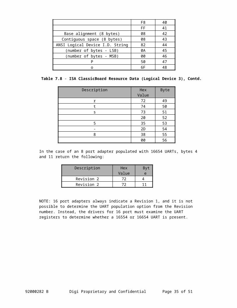
Table 7.15 – ISA ClassicBoard Resource Data (Logical Device 3)
Description Hex Value ByteLogical Device Identifier #3 16 0Function Number (DGI 007) 10 1
(Digi 16C554 UART #2) E9 200 3
Revision (1) 71 4Control Register Support [37:31] / BOOT 02 5
Control Register Support [3F:38] 00 6Compatible Device I.D. 1C 7
Function Number (DGI 007) 10 8(Digi 16C554 UART #2) E9 9
00 10Revision (1) 71 11
I/O Port Descriptor 3a 47 1200 13
(0x100 - 0xFFF8) 00 1401 15F8 16FF 17
Base alignment (8 bytes) 08 18Contiguous space (8 bytes) 08 19
I/O Port Descriptor 3b 47 2000 21
(0x100 - 0xFFF8) 00 2201 23F8 24FF 25
Base alignment (8 bytes) 08 26Contiguous space (8 bytes) 08 27
I/O Port Descriptor 3c 47 2800 29
(0x100 - 0xFFF8) 00 3001 31F8 32FF 33
Base alignment (8 bytes) 08 34Contiguous space (8 bytes) 08 35
I/O Port Descriptor 3d 47 3600 37
(0x100 - 0xFFF8) 00 3801 39F8 40FF 41
Base alignment (8 bytes) 08 42Contiguous space (8 bytes) 08 43
ANSI Logical Device I.D. String 82 44(number of bytes - LSB) 0A 45(number of bytes - MSB) 00 46
P 50 47o 6F 48
92000282 B Digi Proprietary and Confidential Page 26 of 39
Table 7.8 - ISA ClassicBoard Resource Data (Logical Device 3), Contd.
Description Hex Value Byter 72 49t 74 50s 73 51
20 525 35 53- 2D 548 38 55
00 56
In the case of an 8 port adapter populated with 16654 UARTs, bytes 4 and 11 return the following:
Description Hex Value ByteRevision 2 72 4Revision 2 72 11
NOTE: 16 port adapters always indicate a Revision 1, and it is not possible to determine the UART population option from the Revision number. Instead, the drivers for 16 port must examine the UART registers to determine whether a 16554 or 16654 UART is present.
92000282 B Digi Proprietary and Confidential Page 27 of 39
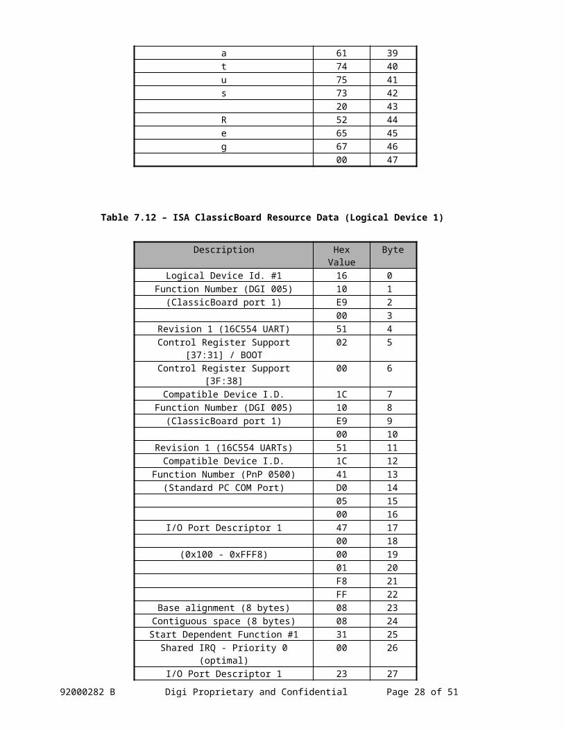
Table 7.16 – ISA ClassicBoard Resource Data (Logical Device 4)
Description Hex Value ByteLogical Device Identifier #4 16 0Function Number (DGI 008) 10 1
(Digi 16C554 UART #3) E9 200 3
Revision (1) 81 4Control Register Support [37:31] / BOOT 02 5
Control Register Support [3F:38] 00 6Compatible Device I.D. 1C 7
Function Number (DGI 008) 10 8(Digi 16C554 UART #3) E9 9
00 10Revision (1) 81 11
I/O Port Descriptor 4a 47 1200 13
(0x100 - 0xFFF8) 00 1401 15F8 16FF 17
Base alignment (8 bytes) 08 18Contiguous space (8 bytes) 08 19
I/O Port Descriptor 4b 47 2000 21
(0x100 - 0xFFF8) 00 2201 23F8 24FF 25
Base alignment (8 bytes) 08 26Contiguous space (8 bytes) 08 27
I/O Port Descriptor 4c 47 2800 29
(0x100 - 0xFFF8) 00 3001 31F8 32FF 33
Base alignment (8 bytes) 08 34Contiguous space (8 bytes) 08 35
I/O Port Descriptor 4d 47 3600 37
(0x100 - 0xFFF8) 00 3801 39F8 40FF 41
Base alignment (8 bytes) 08 42Contiguous space (8 bytes) 08 43
ANSI Logical Device I.D. String 82 44(number of bytes - LSB) 0A 45(number of bytes - MSB) 00 46
P 50 47o 6F 48r 72 49
92000282 B Digi Proprietary and Confidential Page 28 of 39

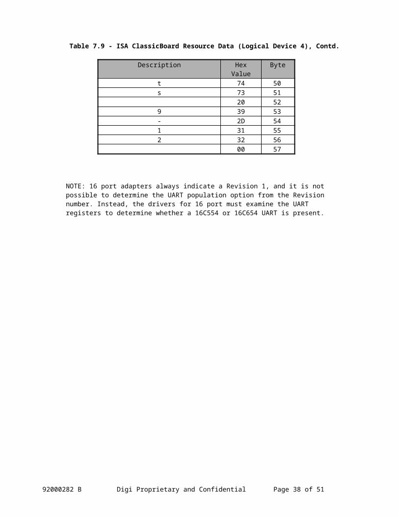
Table 7.9 - ISA ClassicBoard Resource Data (Logical Device 4), Contd.
Description Hex Value Bytet 74 50s 73 51
20 529 39 53- 2D 541 31 552 32 56
00 57
NOTE: 16 port adapters always indicate a Revision 1, and it is not possible to determine the UART population option from the Revision number. Instead, the drivers for 16 port must examine the UART registers to determine whether a 16C554 or 16C654 UART is present.
92000282 B Digi Proprietary and Confidential Page 29 of 39

Table 7.17 – ISA ClassicBoard Resource Data (Logical Device 5)
Description Hex Value ByteLogical Device Identifier #5 16 0Function Number (DGI 009) 10 1
(Digi 16C554 UART #4) E9 200 3
Revision (1) 91 4Control Register Support [37:31] / BOOT 02 5
Control Register Support [3F:38] 00 6Compatible Device I.D. 1C 7
Function Number (DGI 009) 10 8(Digi 16C554 UART #4) E9 9
00 10Revision (1) 91 11
I/O Port Descriptor 5a 47 1200 13
(0x100 - 0xFFF8) 00 1401 15F8 16FF 17
Base alignment (8 bytes) 08 18Contiguous space (8 bytes) 08 19
I/O Port Descriptor 5b 47 2000 21
(0x100 - 0xFFF8) 00 2201 23F8 24FF 25
Base alignment (8 bytes) 08 26Contiguous space (8 bytes) 08 27
I/O Port Descriptor 5c 47 2800 29
(0x100 - 0xFFF8) 00 3001 31F8 32FF 33
Base alignment (8 bytes) 08 34Contiguous space (8 bytes) 08 35
I/O Port Descriptor 5d 47 3600 37
(0x100 - 0xFFF8) 00 3801 39F8 40FF 41
Base alignment (8 bytes) 08 42Contiguous space (8 bytes) 08 43
ANSI Logical Device I.D. String 82 44(number of bytes - LSB) 0A 45(number of bytes - MSB) 00 46
P 50 47o 6F 48
92000282 B Digi Proprietary and Confidential Page 30 of 39

Table 7.10 - ISA ClassicBoard Resource Data (Logical Device 5), Contd.
Description Hex Value Byter 72 49t 74 50s 73 51
20 521 31 533 33 54- 2D 551 31 566 36 57
00 58
NOTE: 16 port adapters always indicate a Revision 1, and it is not possible to determine the UART population option from the Revision number. Instead, the drivers for 16 port must examine the UART registers to determine whether a 16C554 or 16C654 UART is present.Architecture
Table 7.10 - ISA ClassicBoard Resource Data (End Tag)
Description Hex Value ByteEnd TAG 79 0
Resource Data Checksum xx 1
92000282 B Digi Proprietary and Confidential Page 31 of 39

8. APPENDIX B - Interrupt Status decoding
Table 8.18 DigiBoard Mode Interrupt Status
Interrupt pending on Location 0 (Hex) Location 1 (Hex)Port 1 0x00 0x00Port 2 0x01 0x01Port 3 0x02 0x02Port 4 0x03 0x03Port 5 0x04 0x04Port 6 0x05 0x05Port 7 0x06 0x06Port 8 0x07 0x07Port 9 0x08 0x08
Port 10 0x09 0x09Port 11 0x0A 0x0APort 12 0x0B 0x0BPort 13 0x0C 0x0CPort 14 0x0D 0x0DPort 15 0x0E 0x0EPort 16 0x0F 0x0FNone 0xFF 0xFF
Table 8.19 StarGate Mode Interrupt Status
Pending Location 1 Location 0Interrupt MSB LSB MSB LSB
7 6 5 4 3 2 1 0 7 6 5 4 3 2 1 0Port 1 x x x x x x x x x x x x x x x 1Port 2 x x x x x x x x x x x x x x 1 xPort 3 x x x x x x x x x x x x x 1 x xPort 4 x x x x x x x x x x x x 1 x x xPort 5 x x x x x x x x x x x 1 x x x xPort 6 x x x x x x x x x x 1 x x x x xPort 7 x x x x x x x x x 1 x x x x x xPort 8 x x x x x x x x 1 x x x x x x xPort 9 x x x x x x x 1 x x x x x x x xPort 10 x x x x x x 1 x x x x x x x x xPort 11 x x x x x 1 x x x x x x x x x xPort 12 x x x x 1 x x x x x x x x x x xPort 13 x x x 1 x x x x x x x x x x x xPort 14 x x 1 x x x x x x x x x x x x xPort 15 x 1 x x x x x x x x x x x x x xPort 16 1 x x x x x x x x x x x x x x xNone 0 0 0 0 0 0 0 0 0 0 0 0 0 0 0 0
92000282 B Digi Proprietary and Confidential Page 32 of 39
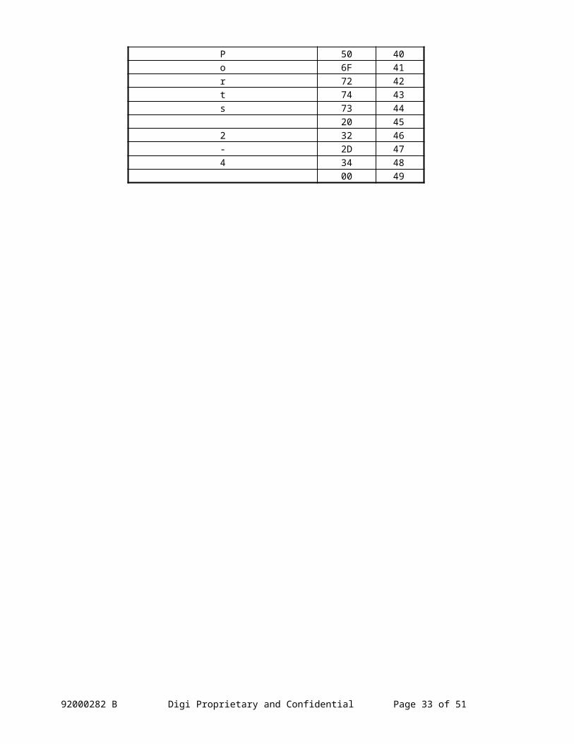
Table 8.20 Arnet Mode Interrupt Status
Pending Location 2Interrupt MSB LSB
7 6 5 4 3 2 1 0Port 1 x x x x x x x 0Port 2 x x x x x x 0 xPort 3 x x x x x 0 x xPort 4 x x x x 0 x x xPort 5 x x x 0 x x x xPort 6 x x 0 x x x x xPort 7 x 0 x x x x x xPort 8 0 x x x x x x xNone 1 1 1 1 1 1 1 1
92000282 B Digi Proprietary and Confidential Page 33 of 39

9. APPENDIX C - PCI Registers
Table 9.21 PCI Header Information
Offset 0 8 16 2400h Vendor ID = 114Fh Device ID = 0028h (4 port) or 0029h (8 port)04h Command Status08h Revision ID = 00h Class Code = 0780h0Ch Cache Line Size Latency Timer Header Type Self Test10h PLX Memory Mapped Configuration Base Address14h PLX I/O Mapped Configuration Base Address18h Local Address Space 0 Base Address –I/O Mapped UARTs and Status1Ch Local Address Space 1 Base Address – Memory Mapped Expansion ROM (not used)20h Local Address Space 2 Base Address – Memory Mapped UARTs and Status24h PCI Address Space 5 – Not used28h CardBus CIS Pointer (not supported)2Ch Subsystem Vendor ID = 114Fh Subsystem ID = 0001h30h Expansion ROM Base Address34h Reserved38h Reserved3Ch INT Line = 00h INT Pin = 01h Min Grant = 00h Max Latency = 01h40h Retry Counter EBI Counter Pre-empt Counter Gen. Counter44h PCREQ Counter Refresh Counter48h - FCh
Device Specific Registers
Table 9.22 Local Address Space 0
Offset 0 8 16 2400h I/O Mapped Quad UART 020h I/O mapped Quad UART 140h I/O mapped Interrupt
Status registerReserved
Table 9.23 Local Address Space 1
Offset 0 8 16 240000h – 03E8h
Memory Mapped Expansion ROM
Table 9.24 Local Address Space 2
Offset 0 8 16 2400h Memory Mapped Quad UART 020h Memory Mapped Quad UART 140h Memory Mapped
Interrupt Status Register
Reserved
92000282 B Digi Proprietary and Confidential Page 34 of 39
10. APPENDIX D - PLX 9052 Registers Table 10.25 PLX Memory Mapped Configuration Registers
Offset 0 8 16 2400h Local Address Space 0 Range Register Description04h Local Address Space 1 Range Register Description08h Local Address Space 2 Range Register Description0Ch Local Address Space 3 Range Register Description10h Expansion ROM Range Register (not used)14h Local Address Space 0 Local Bass Address (Remap Register Description)18h Local Address Space 1 Local Bass Address (Remap Register Description)1Ch Local Address Space 2 Local Bass Address (Remap Register Description)20h Local Address Space 3 Local Bass Address (Remap Register Description)24h Expansion ROM Local Base Address (Remap) Register (not used)28h Local Address Space 0 Bus Region Descriptor Register2Ch Local Address Space 1 Bus Region Descriptor Register30h Local Address Space 2 Bus Region Descriptor Register34h Local Address Space 3 Bus Region Descriptor Register38h Expansion ROM Bus Region Descriptor Register3Ch Chip Select 0 Base Address Register40h Chip Select 1 Base Address Register44h Chip Select 2 Base Address Register48h Chip Select 3 Base Address Register4Ch Interrupt Control/Status Register50h User I/O, PCI Target Response, EEPROM, Initialization Control Register
Table 10.26 Local Address Space X (0,1,2 or 3) Range Register Description
Field Description Read/Write Value After Reset
0 Memory Space Indicator. 0 Indicates Local Address space X maps into PCI memory space. 1 indicates X maps into PCI I/O space.
R/W 0
2:1 If mapped into Memory Space, encoding is as follows:2/1 Meaning0 Locate anywhere in 32 bit PCI address space01 Locate below 1MB in PCI address space10 Locate anywhere in 64 bit PCI address space11 Reserved
If mapped into I/O space bit 1 must be a value of 0.Bit 2 is included with bits 27:3 to indicate decoding range.
R/W 00
3 If mapped into Memory Space, a value of 2 indicates that reads are prefetchable. If mapped into I/O space, bit is included with bits [27:2] to indicate decoding range.
R/W 0
27:4 Specifies PCI address bits used to decode PCI access to local bus space X. Each of the bits corresponds to an address bit. Bit 27 corresponds to address bit 27. A value of 1 indicates the bits should be included in decode. Write a value of 0 to all others. Default is 1MB.
R/W FFFF80
31:28 Unused R 0
92000282 B Digi Proprietary and Confidential Page 35 of 39
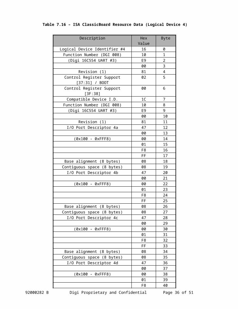
Table 10.27 Local Address Space X (0,1,2 or 3) Bus Region Descriptor Register
Field Description Read/Write Value After Reset
23:22 Bus Width.00 = 8 bit01 = 16 bit10 = 32 bit11 = Reserved
R/W 10
24 Byte Ordering. 1 indicates Bit Endian. 0 indicates Little Endian R/W 025 Big Endian Byte Lane Mode. 1 indicates that in Big Endian mode
byte lanes [31:16] be used for 16 bit local bus and byte lane [31:24] for an 8 bit local bus. A value of 0 indicates that in Big Endian mode byte lanes [15:0] be used for 16 bit local bus, and byte lane [7:0] for an 8 bit local bus.
R/W 0
Table 10.28 Chip Select X (0,1,2 or 3) Base Address Register
Field Description R/W Value after Reset0 Chip Select X Enable. 1 is enabled, 0 is disabled R/W 027:1 Local Base Address of Chip Select X. Write zeroes in the least
significant bits to define the range for Chip Select X. Start from bit 1 and scanning toward bit 27, the first “1” found defines the size. The remaining most significant bits, excluding the first “1” found, defines the base address.
R/W 0
31:28 Unused R 0
Table 10.29 Interrupt Control/Status Register
Field Description R/W Value after Reset0 Local interrupt 1 Enable. 1 indicates enabled, 0 indicates disabled R/W 01 Local Interrupt 1 Polarity. 1 indicate Active high, 0 indicates Active
low.R/W 0
2 Local Interrupt 1 Status. 1 indicates Interrupt active, 0 indicates Interrupt not active
R 0
3 Local Interrupt 2 Enable. 1 indicates enabled, 0 indicates disabled R/W 04 Local Interrupt 2 Polarity. 1 indicate Active high, 0 indicates Active
low.R/W 0
5 Local Interrupt 2 Status. 1 indicates Interrupt active, 0 indicates Interrupt not active
R 0
6 PCI Interrupt Enable. 1 enables PCI interrupt R/W 07 Software Interrupt. 1 generates an interrupt R/W 031:8 Unused R 0
92000282 B Digi Proprietary and Confidential Page 36 of 39
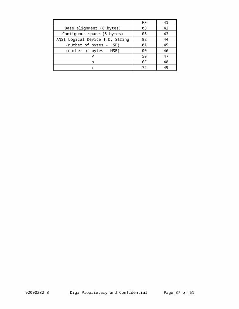
Table 10.30 User I/O, PCI Target Response, EEPROM, Initialization Control Register Description
Field Description R/W Value after Reset
13:12 PCI Configuration Base Address Register (PCIGAR) Enables.00 = PCIBAR0 (Memory) and PCIBAR1 (I/O) enabled.01 = PCIBAR0 (Memory) only.10 = PCIBAR1 (I/O) only.11 = PCIBAR0 (Memory) and PCIBAR1 (I/O) enabled
R/W 0
29 Reload Configuration Registers. When this bit is 0, write a value of 1 causes the PCI 9052 to reload the local configuration registers from EEPROM.
R/W 0
30 PCI Adapter Software Reset. A value of 1 rests the PCI 9052 and issues a reset to the local bus. The contest of the PCI and local configuration registers will not be reset.
R/W 0
92000282 B Digi Proprietary and Confidential Page 37 of 39
11. Appendix E - PCI Reference
11.1 Introduction
This is meant as a brief reference on using a PCI card with the PCI BIOS and its basic operations. It is not meant as a substitute for a full understanding of the PCI Local Bus Specification and PCI BIOS Specification. For more information please consult these references.
11.2 Basic PCI BIOS Calls
If access to the BIOS is available, as with Dos Int1A, several BIOS calls are helpful. Since the device ID (0029h for the 8 port and 0028h for the 4 port) and vendor ID (Digi’s is 114Fh) are known, the device can be found using this information using the BIOS Find PCI Device call. This can be done by loading the registers as follows.
Register Use Value[AH] PCI_FUNCTION_ID B1h[AL] FIND_PCI_DEVICE 02h[CX] Device ID 0029h (or 0028h)[DX] Vendor ID 114Fh[SI] Index 00h
The Index is used if there is more that one board of the same type in a computer. If there is only one board, the Index will always be 00h.
Once these values are loaded into the registers the BIOS can be called either by Int1A or a far call to the BIOS (see PCI BIOS Specification for more details.) This will result in the following information
Register Use Value[BH] Bus Number (0…255)[BL] Device Number - Upper 5 bits
Function Number – Lower 3 bits[AH] Return Code:
SUCCESSFUL 00hDEVICE_NOT_FOUND 86hBAD_VENDOR_ID 83h
[CF] Completion Status Set=error, cleared = success
Since the device and function numbers are now known it is possible to read the data in table 8.1 using the PCI BIOS functions Read Configuration Byte (08h), Word (09h), or Dword (0Ah.) PCI BIOS functions Write Configuration Byte (0Bh), Word (0Ch), and Dword (0Dh) can be used in the same manner to write information to the PCI registers.
Register Use Value[AH] PCI_FUNCTION_ID B1h[AL] READ_CONFIG_DWORD 0Ah[BH] Bus Number (BH from above)[BL] Device Number – Upper 5 bits (BL from above)
Function Number – Lower 3 bits[ECX] Dword value to write For write operations only[DI] Register Number Offset from Beginning
92000282 B Digi Proprietary and Confidential Page 38 of 39

These functions return the following.
Register Use Value[ECX] Dword Read Value in Register read – empty for write[AH] Return Code:
SUCCESSFUL 00hBAD_REGISTER_NUMBER 87h
[CF] Completion Status Set=error, cleared = success
For more in-depth information, please consult the PCI BIOS Specification.
92000282 B Digi Proprietary and Confidential Page 39 of 39