Programmable Solutions for Data Center...
38
Transcript of Programmable Solutions for Data Center...

Topics
• Data Center Trendso Storage, Compute, Networking
• Technology Options
• FPGA Examples
2

Data Center Macro Trends
• Hyper Convergence – Compute/Storage on a single node– Good for Exchange, Oracle, SQL databases– Software-managed including networking and virtualized resources
• Hyper Scale– Independent scaling of compute storage resources– Good for elastic workloads, e.g. Hadoop, Cassandra, noSQL – Also software managed
• IOT– Optimized monitoring of data center resources
• Security– Ingress/egress threat containment across resources – Client to Cloud active monitoring- Symantic, McAfee, Fireeye
• Hybrid Cloud– Public and private resources– Deployment Options, e.g. OpenStack and Docker
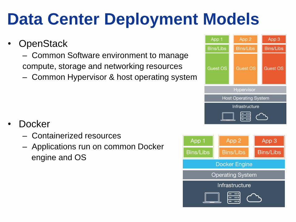
Data Center Deployment Models
• OpenStack– Common Software environment to manage
compute, storage and networking resources
– Common Hypervisor & host operating system
• Docker– Containerized resources
– Applications run on common Docker
engine and OS

Data Center Trends-Storage
• Application specific tiering
• Persistence
• Containers
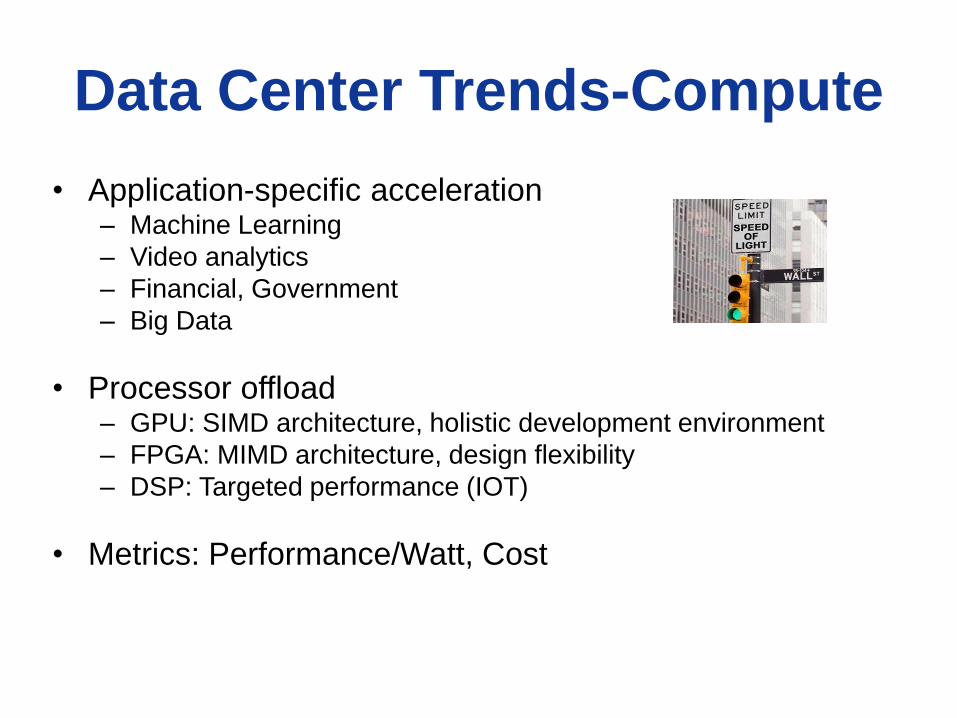
Data Center Trends-Compute
• Application-specific acceleration– Machine Learning
– Video analytics
– Financial, Government
– Big Data
• Processor offload– GPU: SIMD architecture, holistic development environment
– FPGA: MIMD architecture, design flexibility
– DSP: Targeted performance (IOT)
• Metrics: Performance/Watt, Cost

Data Center Trends-Networking
• NVMe over Fabrics– RDMA (iWARP, RoCE), FC– Infiniband– L1 tunneling
OpenFabricsAlliance.org
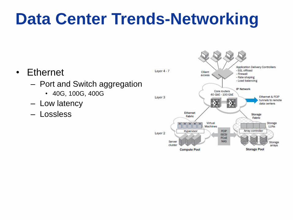
Data Center Trends-Networking
• Ethernet– Port and Switch aggregation
• 40G, 100G, 400G
– Low latency
– Lossless
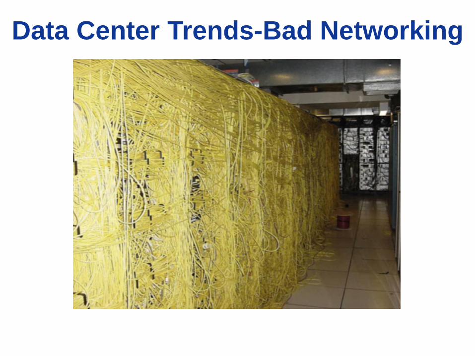
Data Center Trends-Bad Networking
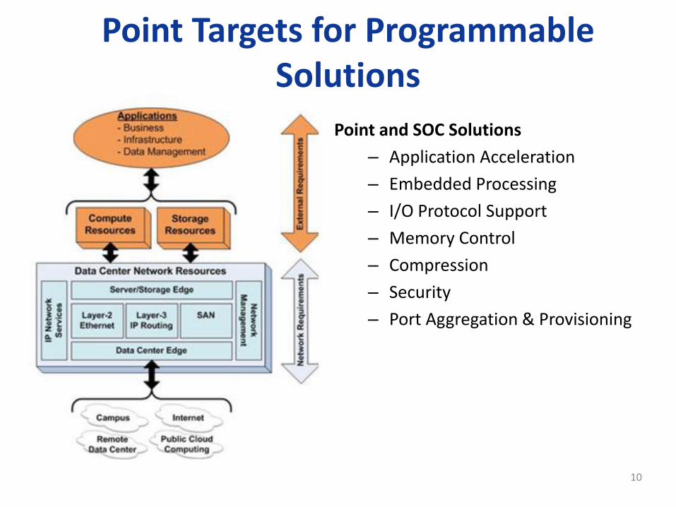
Point Targets for Programmable Solutions
Point and SOC Solutions
– Application Acceleration
– Embedded Processing
– I/O Protocol Support
– Memory Control
– Compression
– Security
– Port Aggregation & Provisioning
10
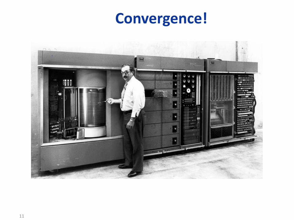
Convergence!
Let’s Win and have Fun!
11
Technology Options
12

Technology scaling favors programmability and parallelism
13
CPUs DSPs Multi-Cores Array GPGPUs FPGAs
Fine-GrainedMassivelyParallelArrays
Single CoresCoarse-GrainedMassivelyParallelProcessorArrays
Multi-CoresCoarse-GrainedCPUs and DSPs
Processing Options

FPGA Architecture
• Massive Parallelism– Millions of logic elements
– Thousands of 20Kb memory blocks
– Thousands of DSP blocks
– Dozens of High-speed transceivers
• Hardware-centric– VHDL/Verilog
– Synthesis
– Place&Route
14
I/O
I/O
I/O
I/O
Programmable
Routing Switch
Logic
Element

GPU Offload Advantage
• Massive Cores–
• Hardware-centric–
15
I/O
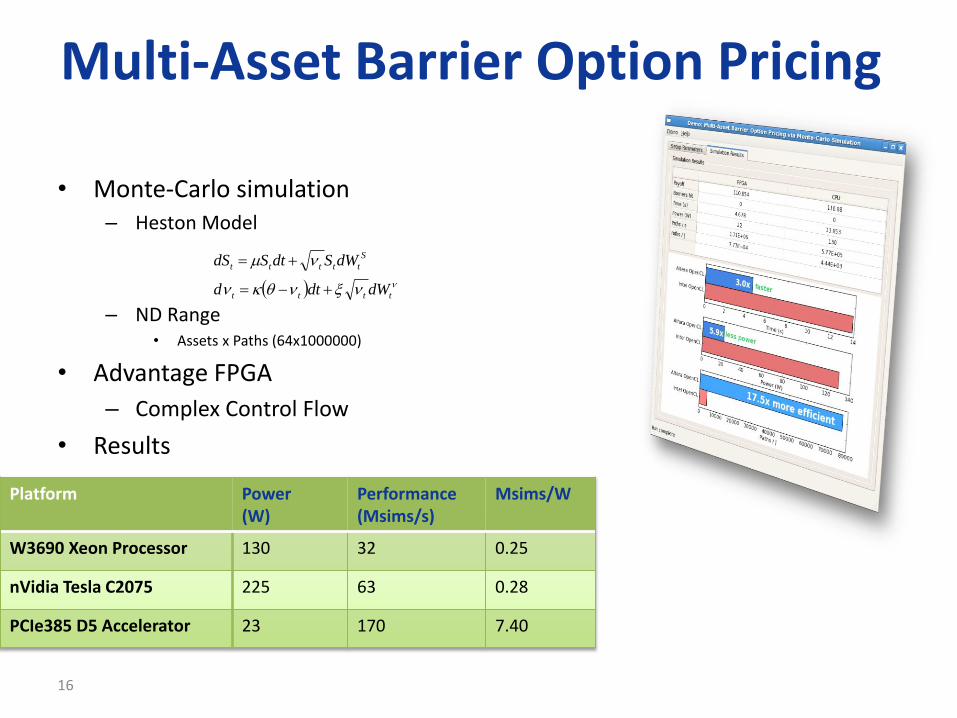
Multi-Asset Barrier Option Pricing
• Monte-Carlo simulation– Heston Model
– ND Range• Assets x Paths (64x1000000)
• Advantage FPGA
– Complex Control Flow
• Results
16
Platform Power(W)
Performance(Msims/s)
Msims/W
W3690 Xeon Processor 130 32 0.25
nVidia Tesla C2075 225 63 0.28
PCIe385 D5 Accelerator 23 170 7.40
tttt
S
ttttt
dWdtd
dWSdtSdS

Storage Trends
17
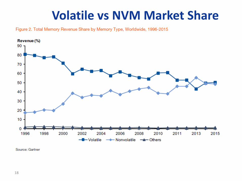
Volatile vs NVM Market Share
18

Revenue Forecast, but wait…
19
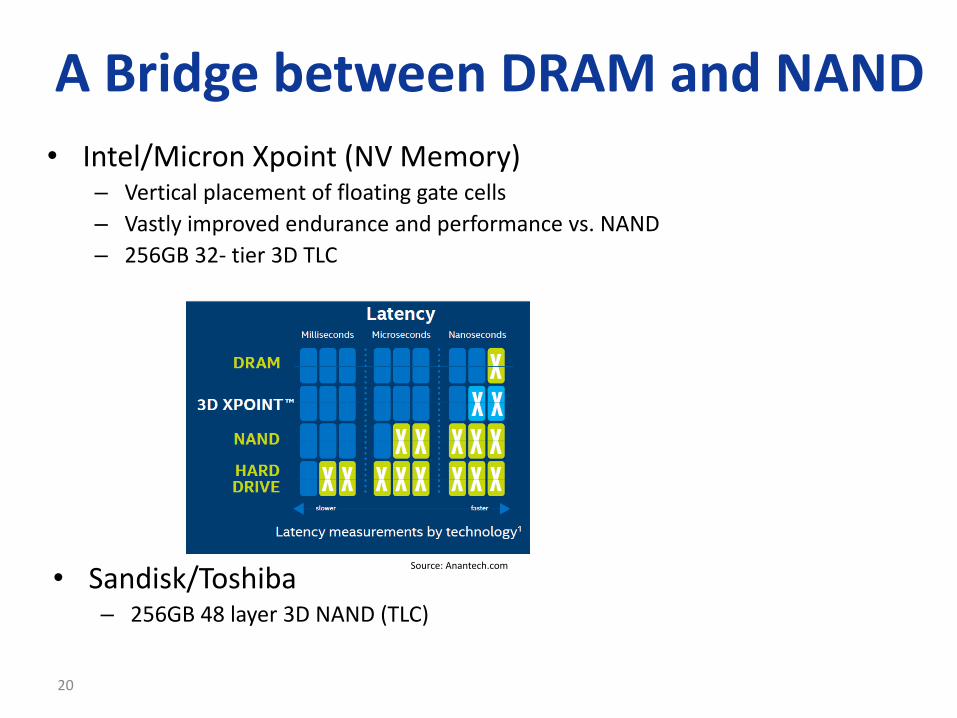
A Bridge between DRAM and NAND
• Intel/Micron Xpoint (NV Memory)– Vertical placement of floating gate cells
– Vastly improved endurance and performance vs. NAND
– 256GB 32- tier 3D TLC
• Sandisk/Toshiba– 256GB 48 layer 3D NAND (TLC)
20
Source: Anantech.com
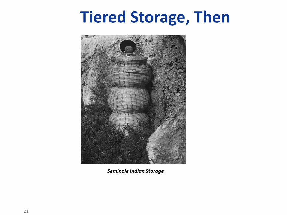
Tiered Storage, Then
21
Seminole Indian Storage
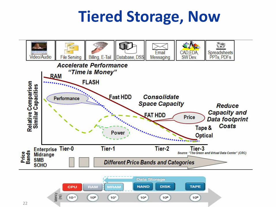
Tiered Storage, Now
22

Memory Comparison
23
Figure 2 shows a comparison of these emerging memory technologies. We compare the properties
of most memory technologies in reading speed (x-axis), endurance (y-axis), cell size (size of the ball)
and switching energy (color of the ball).

Memory Comparisons- Performance
24

Migration Timeline- Cost
25

5MB in Flight!
26

Memory Controller Design Considerations
27
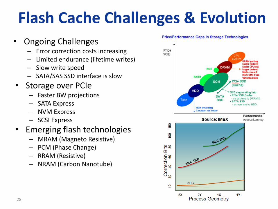
Flash Cache Challenges & Evolution• Ongoing Challenges
– Error correction costs increasing– Limited endurance (lifetime writes)– Slow write speed– SATA/SAS SSD interface is slow
• Storage over PCIe – Faster BW projections– SATA Express – NVM Express– SCSI Express
• Emerging flash technologies– MRAM (Magneto Resistive)– PCM (Phase Change)– RRAM (Resistive)– NRAM (Carbon Nanotube)
28

Flash Controller Design Challenges
Flash Memory Summit 2012Santa Clara, CA 29
Emerging memory types
- ONFI 4.0, Toggle Mode 2.x
- PCM, MRAM
- DDR4 Controller Performance Options
- Write back cache, queuing, interleaving, striping
ECC levels
- BCH, LDPC, Hybrid
FTL location- Host or companion
Data transfer interface support
- PCI Express, SAS/SATA, FC, IB
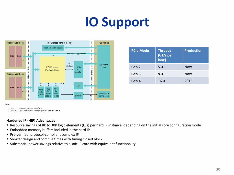
IO Support
30
Hardened IP (HIP) Advantages Resource savings of 8K to 30K logic elements (LEs) per hard IP instance, depending on the initial core configuration mode Embedded memory buffers included in the hard IP Pre-verified, protocol-compliant complex IP Shorter design and compile times with timing closed block Substantial power savings relative to a soft IP core with equivalent functionality
PCIe Roadmap
PCIe Mode Thruput(GT/s per lane)
Production
Gen 2 5.0 Now
Gen 3 8.0 Now
Gen 4 16.0 2016
FPGA Benefits
• FPGAs are a great technology option for Data Centers– Networking: Port aggregation– Compute: Application Acceleration – Storage: Persistent Memory Control
• All development phases supported– Prototyping– Production– Test Validation– Upgrades
31
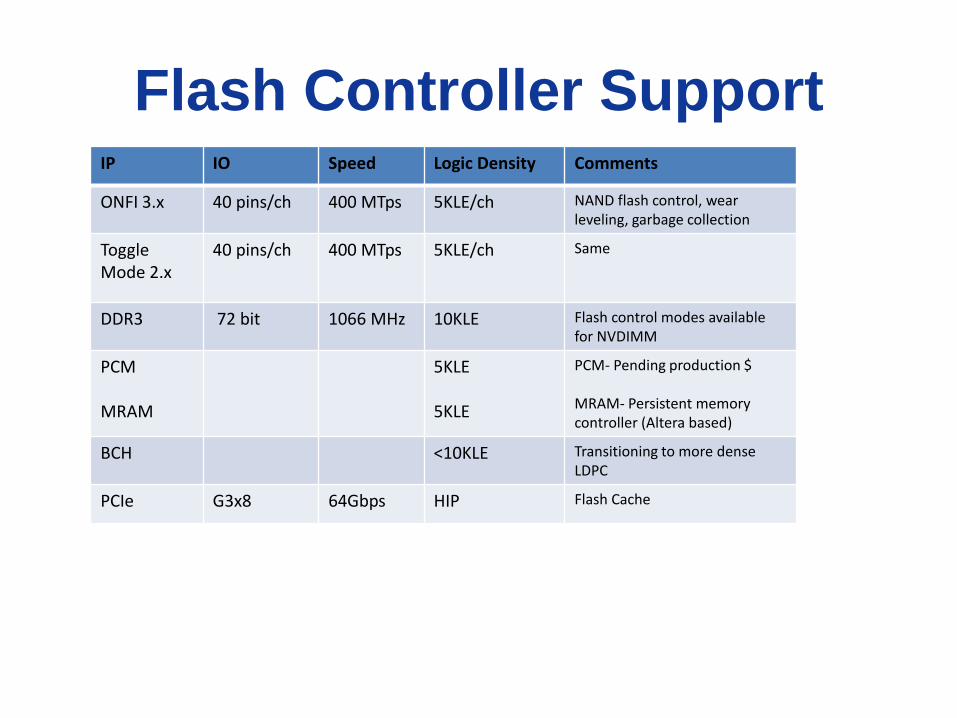
Flash Controller SupportIP IO Speed Logic Density Comments
ONFI 3.x 40 pins/ch 400 MTps 5KLE/ch NAND flash control, wear leveling, garbage collection
Toggle Mode 2.x
40 pins/ch 400 MTps 5KLE/ch Same
DDR3 72 bit 1066 MHz 10KLE Flash control modes available for NVDIMM
PCM
MRAM
5KLE
5KLE
PCM- Pending production $
MRAM- Persistent memory controller (Altera based)
BCH <10KLE Transitioning to more dense LDPC
PCIe G3x8 64Gbps HIP Flash Cache

Hybrid RAID System
- Persistent DRAM and Flash Caches
FC, iSCSI, FCoE
CPU
PCI-e SATA
SAS
Network Side
Persistent
DRAM
FC HBA
PCI-e or CPU System Bus
FC HBA
CPU Interface
Cache/Memory Controller
Network I/F
Disk I/F
RAID² Logic PCI-e
PCI-e
Disk Side
FPGA Controller
ASSPs
RAID/Cache Controller
Flash
Cache
Dual Controller
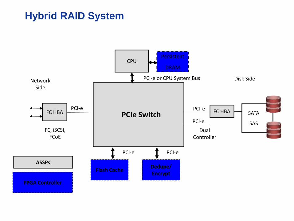
Hybrid RAID System
FC, iSCSI, FCoE
CPU
PCI-eSATA
SAS
Network Side
Persistent
DRAM
FC HBA
PCI-e or CPU System Bus
FC HBA
PCI-e
PCI-e
Disk Side
FPGA Controller
ASSPs
PCIe Switch
Dual Controller
Dedupe/Encrypt
Flash Cache
PCI-e PCI-e
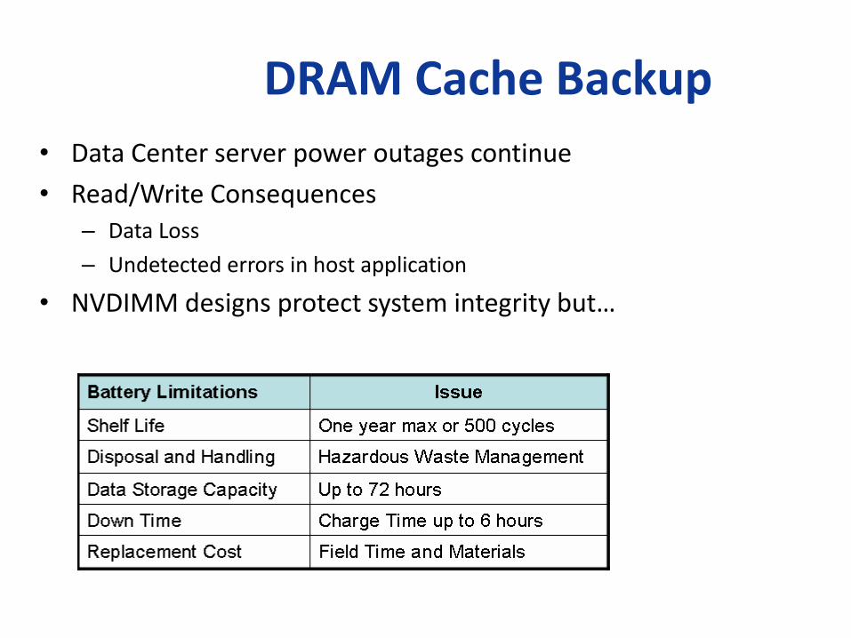
DRAM Cache Backup
• Data Center server power outages continue
• Read/Write Consequences– Data Loss
– Undetected errors in host application
• NVDIMM designs protect system integrity but…
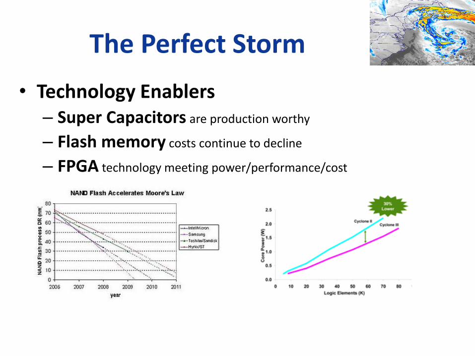
The Perfect Storm
• Technology Enablers– Super Capacitors are production worthy
– Flash memory costs continue to decline
– FPGA technology meeting power/performance/cost
Lower Cost per Process Node Step FPGA Low Power Attributes
37
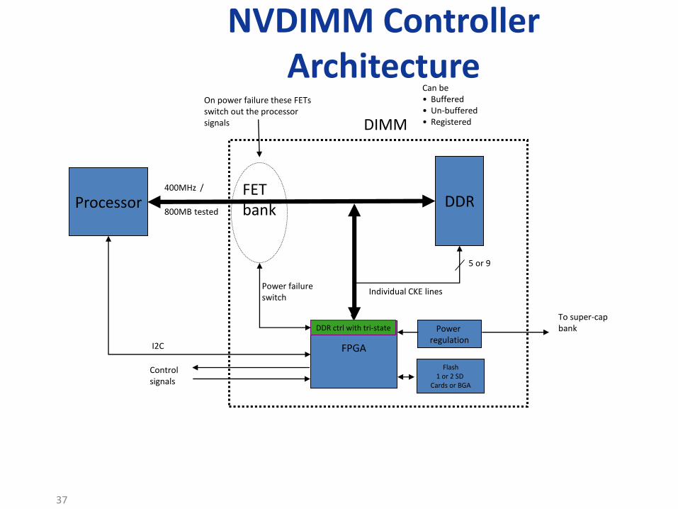
NVDIMM Controller Architecture
Processor DDR
FPGA
FETbank
400MHz /
800MB tested
DIMM
Can be• Buffered• Un-buffered• Registered
On power failure these FETs switch out the processor signals
Flash1 or 2 SD
Cards or BGA
DDR ctrl with tri-state Power regulation
To super-capbank
I2C
Controlsignals
Individual CKE lines
5 or 9
Power failure switch
Summary
38
Storage: disruptive technologies
Compute: new application-specific topologies
Networking: Optimization, convergence and security
Programmable solutions provide flexibility for emerging standards and topologies
Learn more with DS McIntyre Consulting!