Prof. Muhammad Saeed I. 1/27/2015 Computer Architecture & Assembly Language 2.
50
Computer Organization And Assembly Language Prof. Muhammad Saeed I
-
Upload
zachery-clatterbuck -
Category
Documents
-
view
225 -
download
0
Transcript of Prof. Muhammad Saeed I. 1/27/2015 Computer Architecture & Assembly Language 2.

Computer Organization And
Assembly Language
Prof. Muhammad Saeed
I
Computer Architecture & Assembly Language
2
X86 Processor Architecture
1/27/2015

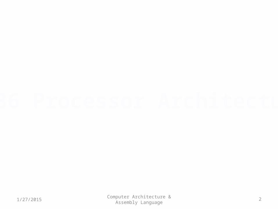
"The number of transistors incorporated in a chip will approximately double every 24 months."
Moor’s Law
END

CISC RISC
Emphasis on hardware Emphasis on software
Includes multi-clockcomplex instructions
Single-clock,reduced instruction only
Memory-to-memory:"LOAD" and "STORE"incorporated in instructions
Register to register:"LOAD" and "STORE"are independent instructions
Small code sizes,high cycles per second
Low cycles per second,large code sizes
Transistors used for storingcomplex instructions
Spends more transistorson memory registers
Comparison Of CISC & RISC Technologies

Intel 4004
Year 1971
Clock Speed 740 KHz
No. Of Transistors 2300 at 10 m
MIPS 0.07
Register Length 4-bit
Data Bus Length 4-bit
Address Memory 640 bytes
First single-chip microprocessor

Intel 8008
Year 1972
Clock Speed 800 KHz
No. Of Transistors 3500 at 10 m
MIPS 0.05
Register Length 8-bit
Data Bus Length 8-bit
Address Memory 16 kb
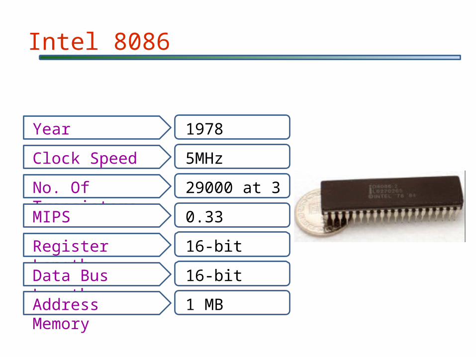
Intel 8086
Year 1978
Clock Speed 5MHz
No. Of Transistors 29000 at 3 m
MIPS 0.33
Register Length 16-bit
Data Bus Length 16-bit
Address Memory 1 MB

Intel 8088
Year 1979
Clock Speed 5MHz
No. Of Transistors 29000 at 3 m
MIPS 0.33
Register Length 16-bit
Data Bus Length Ext 8-bit
Address Memory 1 MB

Intel 80286
Year 1982
Clock Speed 6-25MHz
No. Of Transistors 134000 at 1.5 m
MIPS 0.9-2.66
Register Length 16-bit
Data Bus Length 16-bit
Addressable Memory 16 MB
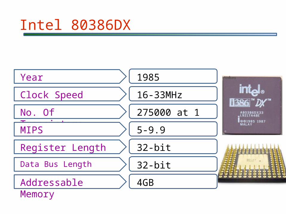
Year 1985
Clock Speed 16-33MHz
No. Of Transistors 275000 at 1 m
MIPS 5-9.9
Register Length 32-bit
Data Bus Length 32-bit
Addressable Memory 4GB
Intel 80386DX

Intel 80486DX
Year 1989
Clock Speed 25-50MHz
No. Of Transistors 1.2million at 1-0.8 m
MIPS 11.1 MIPS at 33 MHz
Register Length 32-bit
Data Bus Length 32-bit
Addressable Memory 4GB
Includes Math Coprocessor and Cache

Intel Pentium 1
Year 1993
Clock Speed 60-200MHz
No. Of Transistors 3.1-5.5million at .8-.35 m
MIPS 100-270
Register Length 32-bit
Data Bus Length 64-bit
Addressable Memory 4GB
Includes data and Instruction Caches(8k)

Intel Pentium
MMX TechnologyThe MMX technology consists of three improvements over the non-MMX Pentium microprocessor: 57 new microprocessor instructions have been added that
are designed to handle video, audio, and graphical data more efficiently.
A new process, Single Instruction Multiple Data ( SIMD ), makes it possible for one instruction to perform the same operation on multiple data items.
The memory cache on the microprocessor has increased to 32 thousand bytes, meaning fewer accesses to memory that is off the microprocessor.

Computer Architecture & Assembly Language
151/27/2015
32-Bit MMX and XMM Registers
MMX Registers: MMX technology improves the performance of Intel processors when implementing advanced multimedia and communications applications. The eight 64-bit MMX registers support special instructions called SIMD (Single-Instruction, Multiple-Data). As the name implies, MMX instructions operate in parallel on the data values contained in MMX registers.
XMM Registers:The x86 architecture also contains eight 128-bit registers called XMM registers. They are used by streaming SIMD extensions to the instruction set.

Intel Pentium II
Year 1997
Clock Speed 450MHz
No. Of Transistors 7.5million at .35-.25 m
MIPS 100-112
Register Length 32-bit
Data Bus Length 64-bit
Addressable Memory 4GB
Includes data and Instruction Caches(8k)
541 MIPS at 200 MHz

Intel Pentium III
Year 1999
Clock Speed 600MHz
No. Of Transistors 9.5million at .35-.25 m
MIPS 2,054 MIPS at 600 MHz
Register Length 32-bit
Data Bus Length 64-bit
Addressable Memory 64G B

Intel Pentium IV
Year 2000-2008
Clock Speed 1.3GHz
No. Of Transistors 55 million at 13 nm
MIPS 9,726 MIPS at 3.2 GHz
Register Length 32-bit
Data Bus Length 64-bit
Addressable Memory 64G B
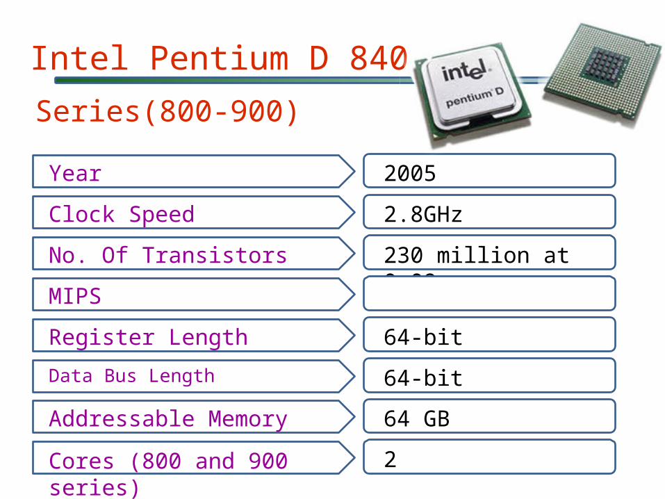
Intel Pentium D 840
Year 2005
Clock Speed 2.8GHz
No. Of Transistors 230 million at 0.09 μm
MIPS
Register Length 64-bit
Data Bus Length 64-bit
Addressable Memory 64 GB
Cores (800 and 900 series) 2
Series(800-900)

Intel i7
Year 2008
Clock Speed 3.2 GHz
No. Of Transistors 731,000,000 45 nm-14nm
MIPS 298,190 MIPS at 3.0 GHz
Register Length 64-bit
Data Bus Length 64-bit
Addressable Memory 64GB

Computer Architecture & Assembly Language
211/27/2015
Intel Chipset Block Diagram

Computer Architecture & Assembly Language
22
Block Diagram of a Microcomputer
1/27/2015
Computer Architecture & Assembly Language
23
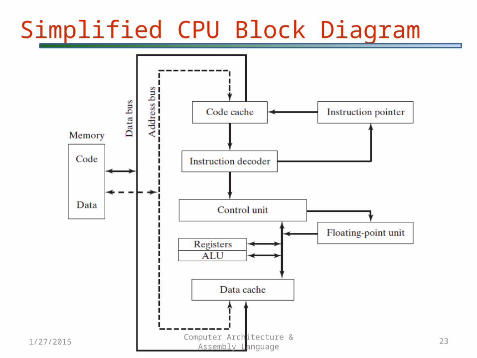
Simplified CPU Block Diagram
1/27/2015

Computer Architecture & Assembly Language
24
32-Bit General Purpose Registers
1/27/2015

Computer Architecture & Assembly Language
25
General Purpose Registers
1/27/2015

Computer Architecture & Assembly Language
26
Floating Point Unit Registers
1/27/2015
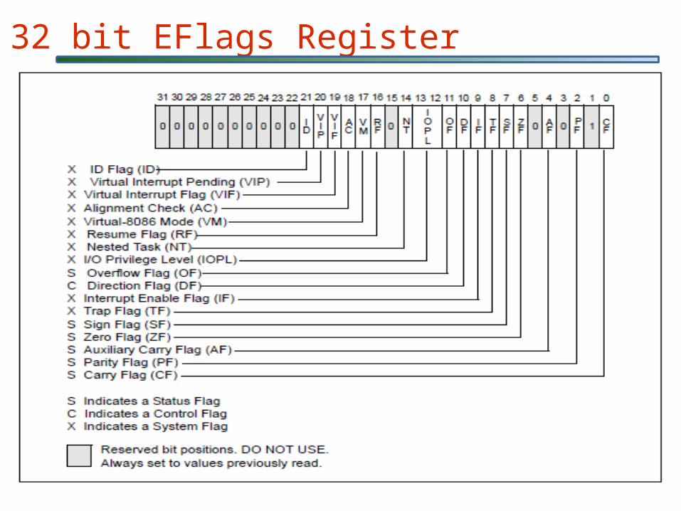
32 bit EFlags Register

Computer Architecture & Assembly Language
28
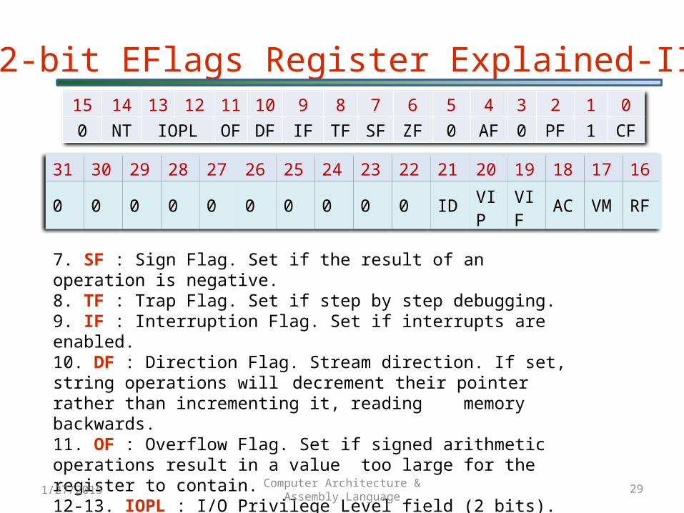
31 30 29 28 27 26 25 24 23 22 21 20 19 18 17 16
0 0 0 0 0 0 0 0 0 0 ID VIP VIF AC VM RF
15 14 13 12 11 10 9 8 7 6 5 4 3 2 1 00 NT IOPL OF DF IF TF SF ZF 0 AF 0 PF 1 CF
32-bit EFlags Register Explained-I
0. CF : Carry Flag. Set if the last arithmetic operation carried (addition) or borrowed (subtraction) a bit beyond the size of the register. This is then checked when the operation is followed with an add-with-carry or subtract-with-borrow to deal with values too large for just one register to contain.
2. PF : Parity Flag. Set if the number of set bits in the least significant byte is a multiple of 2.
4. AF : Adjust Flag. (Auxiliary Carry Flag)Carry of Binary Code Decimal (BCD) numbers arithmetic operations.
6. ZF : Zero Flag. Set if the result of an operation is Zero (0).
1/27/2015
Computer Architecture & Assembly Language
29
31 30 29 28 27 26 25 24 23 22 21 20 19 18 17 16
0 0 0 0 0 0 0 0 0 0 ID VIP VIF AC VM RF
15 14 13 12 11 10 9 8 7 6 5 4 3 2 1 00 NT IOPL OF DF IF TF SF ZF 0 AF 0 PF 1 CF
32-bit EFlags Register Explained-II
7. SF : Sign Flag. Set if the result of an operation is negative.8. TF : Trap Flag. Set if step by step debugging.9. IF : Interruption Flag. Set if interrupts are enabled.10. DF : Direction Flag. Stream direction. If set, string operations will decrement their pointer rather than incrementing it, reading memory backwards.11. OF : Overflow Flag. Set if signed arithmetic operations result in a value
too large for the register to contain.12-13. IOPL : I/O Privilege Level field (2 bits). I/O Privilege Level of the
current process.
1/27/2015

Computer Architecture & Assembly Language
30
31 30 29 28 27 26 25 24 23 22 21 20 19 18 17 16
0 0 0 0 0 0 0 0 0 0 ID VIP VIF AC VM RF
15 14 13 12 11 10 9 8 7 6 5 4 3 2 1 00 NT IOPL OF DF IF TF SF ZF 0 AF 0 PF 1 CF
32-bit EFlags Register Explained-III
14. NT : Nested Task flag. Controls chaining of interrupts. Set if the current process is linked to the next process.16. RF : Resume Flag. Response to debug exceptions.17. VM : Virtual-8086 Mode. Set if in 8086 compatibility mode.18. AC : Alignment Check. Set if alignment checking of memory references is done.19. VIF : Virtual Interrupt Flag. Virtual image of IF.20. VIP : Virtual Interrupt Pending flag. Set if an interrupt is pending.21. ID : Identification Flag. Support for CPUID instruction if can be set.
1/27/2015

Computer Architecture & Assembly Language
31
64-bit RFlags Register
Higher 32 bits are reserved, lower 32 bits are the same as 32-Bit EFlags Register.
1/27/2015

Computer Architecture & Assembly Language
321/27/2015
It is backward-compatible with the x86 instruction set. Addresses are 64 bits long, allowing for a virtual address
space of size 264 bytes. In current chip implementations, only the lowest 48 bits are used.
It can use 64-bit general-purpose registers, allowing instructions to have 64-bit integer operands.
It uses eight more general-purpose registers than the x86. It uses a 48-bit physical address space, which supports up
to 256 terabytes of RAM.
Essential Features Of 64-Bit Processor

General Purpose Registers 16-64 Bits
Sixteen 128-bit XMM registers

Computer Architecture & Assembly Language
34
Memory - I
• ROM is permanently burned into a chip and cannot be erased.• EPROM can be erased slowly with ultraviolet light and reprogrammed.• DRAM, commonly known as main memory, is where programs and data are kept when a program is running. It is inexpensive, but must be refreshed every millisecond to avoid losing its contents. Some systems use ECC (error checking and correcting) memory.• SRAM is used primarily for expensive, high-speed cache memory. It does not have to be refreshed. CPU cache memory is comprised of SRAM.• VRAM holds video data. It is dual ported, allowing one port to continuously refresh the display while another port writes data to the display.• CMOS RAM on the system motherboard stores system setup information. It is refreshed by a battery, so its contents are retained when the computer’s power is off.
• VOLATILE and DYNAMIC
1/27/2015

Computer Architecture & Assembly Language
35
Memory - II (Cache Memory-I)
Caches function as read and write caches when they are involved in the transfer of data from a faster device to a slower device. It allows you send information and then undertake a new task while it translates the data.
L1 cache, which stands for Level 1 cache, primary cache, is a type of small and fast memory that is built into the central processing unit.
L2 cache, L2, or Level 2, cache is used to store recently accessed information. Also known as secondary cache, it is designed to reduce the time needed to access data in cases where data has already been accessed previously. It is slower than L1. It may or may not be in the CPU.
L3 cache, or Level 3, cache is a memory cache that is built into the motherboard. It is used to feed the L2 cache, and is typically faster than the system’s main memory, but still slower than the L2 cache.
1/27/2015

Computer Architecture & Assembly Language
36
Memory - II (Cache Memory-II)
1/27/2015

Computer Architecture & Assembly Language
37
Core 1
L1
Core 2
L1
Core 3
L1
Core 4
L1
L 2 Cache
Core 1
L1
Core 2
L1
Core 3
L1
Core 4
L1
L 2 L 2
L 2 L 2
A quad-core chip with shared L2 Cache A quad-core chip with separate L2 Cache
Memory - II (Cache Memory-III)
1/27/2015

Computer Architecture & Assembly Language
38
Microprocessor
Registers
L1 Cache
L2 Cache
Memory
Disk, Tape, etc
Memory Bus
I/O Bus
Fas
ter
Big
ger
Memory - II (Cache Memory-IV)
1/27/2015

Computer Architecture & Assembly Language
39
Processor Modes Real Mode: A processor running in real mode acts like 8088.
It accesses memory with the same restrictions of the original 8088: a limit of 1 MB of addressable RAM, and it doesn't take advantage of the full 32-bit processing of modern CPUs. All processors have this real mode available.
Protected Mode:• Full access to all of the system's memory. • Ability to multitask.• Support for virtual memory.• 32-bit processing
Virtual Real Mode: It emulates real mode from within protected mode, allowing DOS programs to run. A protected mode operating system such as Windows can in fact create multiple virtual real mode machines, each of which appear to the software running them as if they are the only software running on the machine. Each virtual machine gets its own 1 MB address space, an image of the real hardware BIOS routines, everything.1/27/2015

Computer Architecture & Assembly Language
40
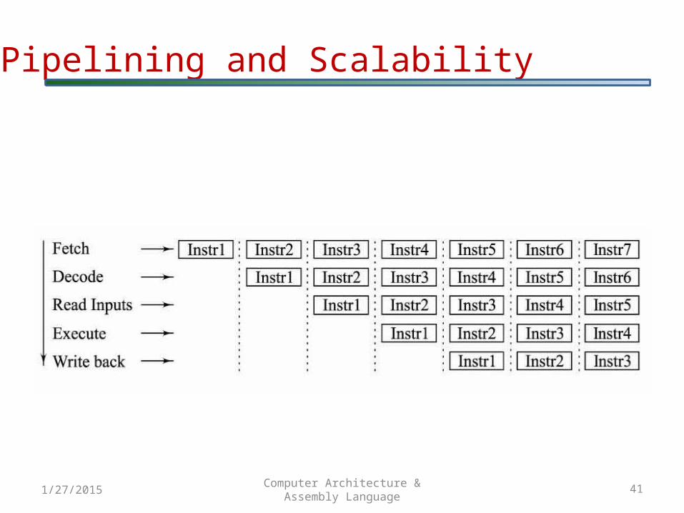
Fetch Unit
Decode Unit
Execute Unit
Pipeline
Fetch Unit
Decode Unit
Fetch Unit
Decode Unit
Holding Buffer
Execute Unit
Execute Unit
Execute Unit
Superscalar
Pipelining and Scalability
1/27/2015
Computer Architecture & Assembly Language
41
Pipelining and Scalability
1/27/2015

Computer Architecture & Assembly Language
421/27/2015
Device port. Serial Port. Parallel Port USB (Universal Serial Bus)
The computer acts as the host.Up to 127 devices can connect to the host, either
directly or by way of USB hubs.Individual USB cables can run as long as 5 meters; with hubs, devices can be up to 30 meters.With USB 2.0,the bus has a maximum data rate of 480
megabits per second . With USB 3.0, data rate is 5 gbits/sec. While USB 2.0 can only send data in one direction at a time, USB 3.0 can transmit data in both directions simultaneously. USBs of >1 TB capacity are available.
Ports
Computer Architecture & Assembly Language
431/27/2015
A bus is a collection of tracesTraces are thin electrical connections that
transport information between hardware devices
A port is a bus that connects exactly two devices
An I/O channel is a bus shared by several devices to perform I/O operations• Handle I/O independently of the system’s
main processors
BUS

Computer Architecture & Assembly Language
44
8088 Block Diagram
1/27/2015
Computer Architecture & Assembly Language
45
Instruction Execution Cycle
Fetch the next operation• Place it in the queue• Update the program counter
Decode the Instruction• Perform address translation• Fetch Operands from memory
Execute the Instruction• Perform the required calculation• Store results in memory or registers• Set status flags attached to the CPU
1/27/2015

Computer Architecture & Assembly Language
46
Memory Address
Segment Address 0EBD
Offset Address00AC
Logical AddressSegment:Offset 0EBD:00AC
Physical Addresssegment x 16 + offset0EBD x 10h + 00AC0EBD0 + 00AC = 0EC7C
Flat Address32-Bit: FF0084C5
1/27/2015

Computer Architecture & Assembly Language
471/27/2015
Global Descriptor Table (GDT) A single GDT is created when the operating system switches the processor into protected mode during boot up. Its base address is held in the GDTR (global descriptor table register). The table contains entries (called segment descriptors) that point to segments. The operating system has the option of storing the segments used by all programs in the GDT.
Local Descriptor Tables (LDT) In a multitasking operating system, each task or program is usually assigned its own table of segment descriptors, called an LDT. The LDTR register contains the address of the program’s LDT. Each segment descriptor contains the base address of a segment within the linear address space. This segment is usually distinct from all other segments
Memory Address

48
Memory AddressThree different logical addresses are shown, each selecting a different entry in the LDT. In this figure we assume that paging is disabled, so the linear address space is also the physical address space.
Computer Architecture & Assembly Language1/27/2015

Computer Architecture & Assembly Language
49
Block Diagram Of Pentium
1/27/2015

END