Product Introduction of MG3710A Vector Signal Generator · CDMA2000 1x/1xEV-DO, AWGN, ... Phase...
66
Product Introduction MG3710A Vector Signal Generator
Transcript of Product Introduction of MG3710A Vector Signal Generator · CDMA2000 1x/1xEV-DO, AWGN, ... Phase...

Product Introduction
MG3710A Vector Signal Generator

Slide 1
MG3710A-E-L-1
MG3710A Vector Signal Generator
Product Introduction
ANRITSU CORPORATION
Version 3.00
March 2013

Slide 2
MG3710A-E-L-1
MG3710A Features
AWGN generator [Opt.049/079]
AM/FM/M/PM Functions [Standard]
Additional analog modulation input option (Opt.050/080)
Supports modulation by external signal input.
Key Performance and Functions Frequency range: [Option]
100 kHz to 2.7/4.0/6.0 GHz
Wide vector modulation bandwidth
160 MHz* /120 MHz (Internal baseband generator)
Sampling Rate
20 kHz to 200 MHz* /160 MHz
SSB Phase noise
< –140 dBc/Hz nominal (100 MHz, 20-kHz offset, CW)
< –131 dBc/Hz typ. (1 GHz, 20-kHz offset)
ACLR performance
–71 dBc (W-CDMA, TestModel1, 64DPCH, 2 GHz)
High power output [Opt.041/071]
+23 dBm (CW, 400 MHz to 3 GHz)
Fast switching speed
< 600 µs (List/Sweep Mode)
High level accuracy
±0.5 dB (Absolute level accuracy)
±0.2 dB typ. (Linearity)
Multi RF output [option]
Two RF outputs @ RF x 2
Baseband signal combine function @ RF x 1
Large-capacity baseband memory [option]
64/256/1024 Msamples
BER test function [Opt.021]
Input Bit Rate: 100 bps to 40 Mbps
Supports Various Communication Systems
Pre-installed Waveform Patterns:
LTE-FDD/TDD (E-TM1.1 to E-TM3.3),
W-CDMA/HSDPA, GSM/EDGE, PDC, PHS,
CDMA2000 1x/1xEV-DO, AWGN,
WLAN (IEEE802.11a/11b/11g), Mobile WiMAX,
Bluetooth®, GPS,
Digital Broadcast (ISDB-T/BS/CS/CATV)
Waveform Patterns [Software & license optional]
DFS Radar Pattern [for TELEC/FCC]
DFS(ETSI) Waveform Pattern
ISDB-Tmm Waveform Pattern
IQproducer [Software license optional]
Waveform generation software
3GPP LTE/LTE-Advanced (FDD),
3GPP LTE/LTE-Advanced (TDD),
HSDPA/HSUPA, W-CDMA, TD-SCDMA,
WLAN 11ac/a/b/g/n/j/p, Mobile WiMAX,
TDMA (PDC, PHS, ARIB, etc.)
CDMA2000 1xEV-DO, DVB-T/H,
Multi-carrier, Fading
∗: Supports firmware version 2.00.00 and later.
Only when using MX370111A WLAN IQproducer and MX370111A-002 802.11ac (160 MHz) option.
New

Slide 3
MG3710A-E-L-1
Supports Various Communication Systems
LTE-FDD/TDD (E-TM1.1 to 3.3)
W-CDMA, GSM/EDGE,
CDMA2000 1x/1xEV-DO
WLAN (IEEE802.11a/b/g)
Mobile WiMAX, AWGN,
Bluetooth, GPS, PDC, PHS,
Digital Broadcast (ISDB-T/BS/CS/CATV)
Pre-installed waveform patterns
Waveform Pattern [option]
DFS Radar Pattern (for TELEC, FCC)
DFS (ETSI) Waveform Pattern
ISDB-Tmm Waveform Pattern
IQproducer [Option]
Any IQ data
- C language
- MATLAB
-Microwave Office
etc.
Waveform patterns
with fixed parameters
PC application software to generate
waveform patterns by setting
parameters at PC
W-CDMA, HSDPA/HSUPA,
TDMA, Multi-carrier, Mobile WiMAX,
3GPP LTE/LTE-Advanced (FDD),
3GPP LTE/LTE-Advanced (TDD),
DVB-T/H, Fading, XG-PHS,
WLAN IEEE802.11ac/a/b/g/j/n/p
TD-SCDMA
Anritsu product
Customer's item
The waveform patterns
are arbitrarily generated.
IQ sample data files (in ASCII format)
programmed by using general EDA
(Electronic Design Automation) tools
such as MATLAB® can also be
converted to waveform patterns for
MG3710A. And a custom-made
waveform pattern file can be
generated arbitrarily.
New

Slide 4
MG3710A-E-L-1
Basic Performance (1/5)
Frequency Range [Option]
100 kHz to 2.7/4.0/6.0 GHz [1stRF: Opt-032/034/036]
[2ndRF: Opt-062/064/066]
The MG3710A supports two built-in vector signal
generators with two RF units (1stRF and optional
2ndRF).
Not only different frequencies but also different levels
and waveform patterns can be set independently at
each SG while each is tracking the other.
1: Supported frequency bands cannot be changed after shipment.
2: IQ input/output is supported only by SG1 (1stRF) and requires Opt-017.
Wide Vector Modulation Bandwidth:
160 MHz*/120 MHz
SSB Phase Noise
<–140 dBc/Hz nominal (100 MHz, 20-kHz offset, CW)
<–131 dBc/Hz typ. (1 GHz, 20-kHz offset, CW)
<–125 dBc/Hz typ. (2 GHz, 20-kHz offset, CW)
Level Accuracy:
Absolute level accuracy: 0.5 dB
Linearity: 0.2 dB typ.
1 2 3 4 5 6
1
10
100
Bandwidth
MHz
Frequency GHz
GSM
WLAN
(11ac
11n
11a)
WMAN
(16e)
120
15
2.7
LTE
LTE-Adv
WMAN EDGE
WLAN(11n/11b/11g)
cdma2000
TD-SCDMA W-CDMA
LTE
LTE-Adv
PDC
PHS
160
(using internal baseband signal generator)
Sampling Rate : 20kHz to 200MHz*/160 MHz An RF modulation bandwidth of 160 MHz is supported using
internal baseband signal generation.
∗: Supports firmware version 2.00.00 and later.
Only when using MX370111A WLAN IQproducer and MX370111A-002 802.11ac (160 MHz) option.
Slide 5
MG3710A-E-L-1
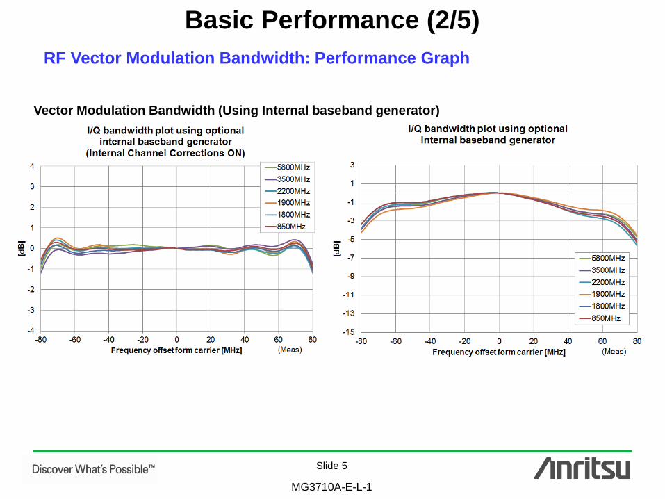
RF Vector Modulation Bandwidth: Performance Graph
Basic Performance (2/5)
Vector Modulation Bandwidth (Using Internal baseband generator)
Slide 6
MG3710A-E-L-1
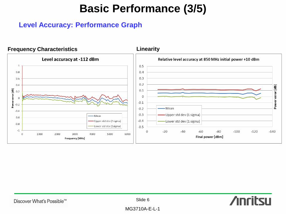
Frequency Characteristics Linearity
Basic Performance (3/5)
Level Accuracy: Performance Graph
Slide 7
MG3710A-E-L-1
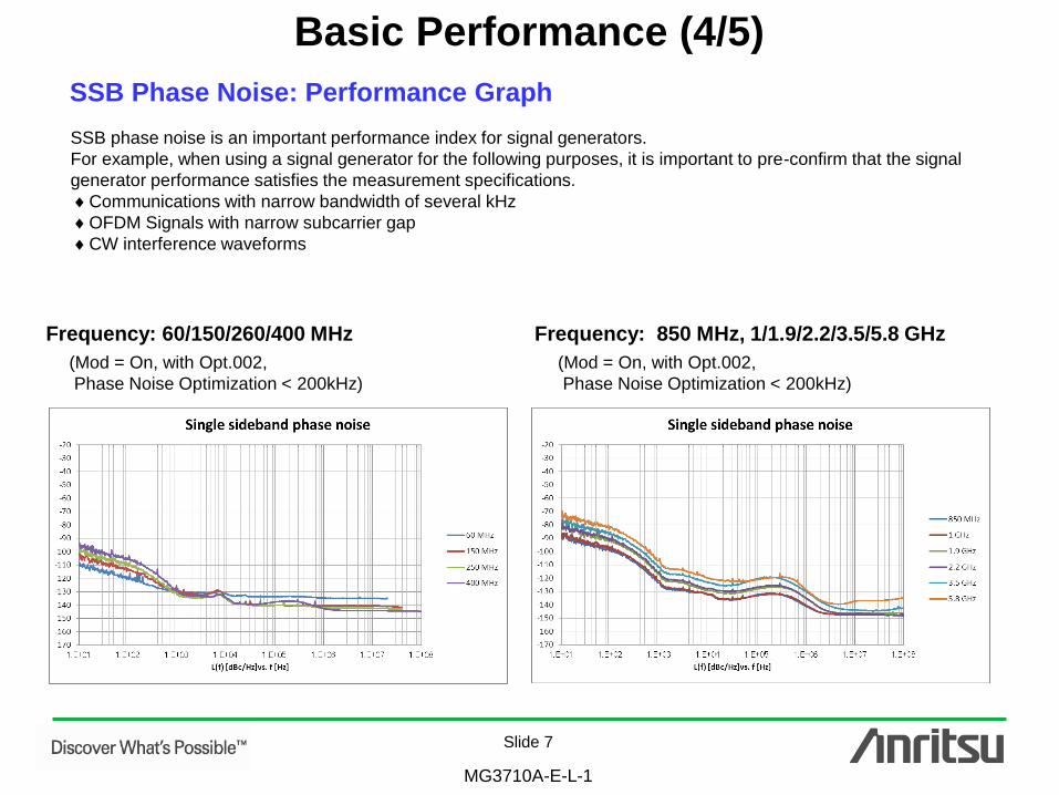
SSB Phase Noise: Performance Graph
Basic Performance (4/5)
SSB phase noise is an important performance index for signal generators.
For example, when using a signal generator for the following purposes, it is important to pre-confirm that the signal
generator performance satisfies the measurement specifications.
Communications with narrow bandwidth of several kHz
OFDM Signals with narrow subcarrier gap
CW interference waveforms
Frequency: 60/150/260/400 MHz
(Mod = On, with Opt.002,
Phase Noise Optimization < 200kHz)
Frequency: 850 MHz, 1/1.9/2.2/3.5/5.8 GHz
(Mod = On, with Opt.002,
Phase Noise Optimization < 200kHz)
Slide 8
MG3710A-E-L-1
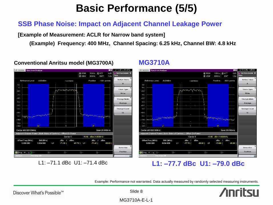
SSB Phase Noise: Impact on Adjacent Channel Leakage Power
Basic Performance (5/5)
(Example) Frequency: 400 MHz, Channel Spacing: 6.25 kHz, Channel BW: 4.8 kHz
[Example of Measurement: ACLR for Narrow band system]
Conventional Anritsu model (MG3700A)
L1: –71.1 dBc U1: –71.4 dBc L1: –77.7 dBc U1: –79.0 dBc
MG3710A
Example: Performance not warranted. Data actually measured by randomly selected measuring instruments.
Slide 9
MG3710A-E-L-1
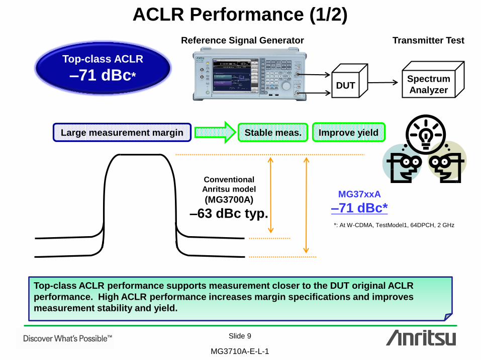
ACLR Performance (1/2)
Conventional
Anritsu model
(MG3700A)
–63 dBc typ.
MG37xxA
–71 dBc*
Top-class ACLR performance supports measurement closer to the DUT original ACLR
performance. High ACLR performance increases margin specifications and improves
measurement stability and yield.
DUT
Reference Signal Generator
Spectrum
Analyzer
Large measurement margin Stable meas. Improve yield
Top-class ACLR
–71 dBc*
Transmitter Test
*: At W-CDMA, TestModel1, 64DPCH, 2 GHz
Slide 10
MG3710A-E-L-1
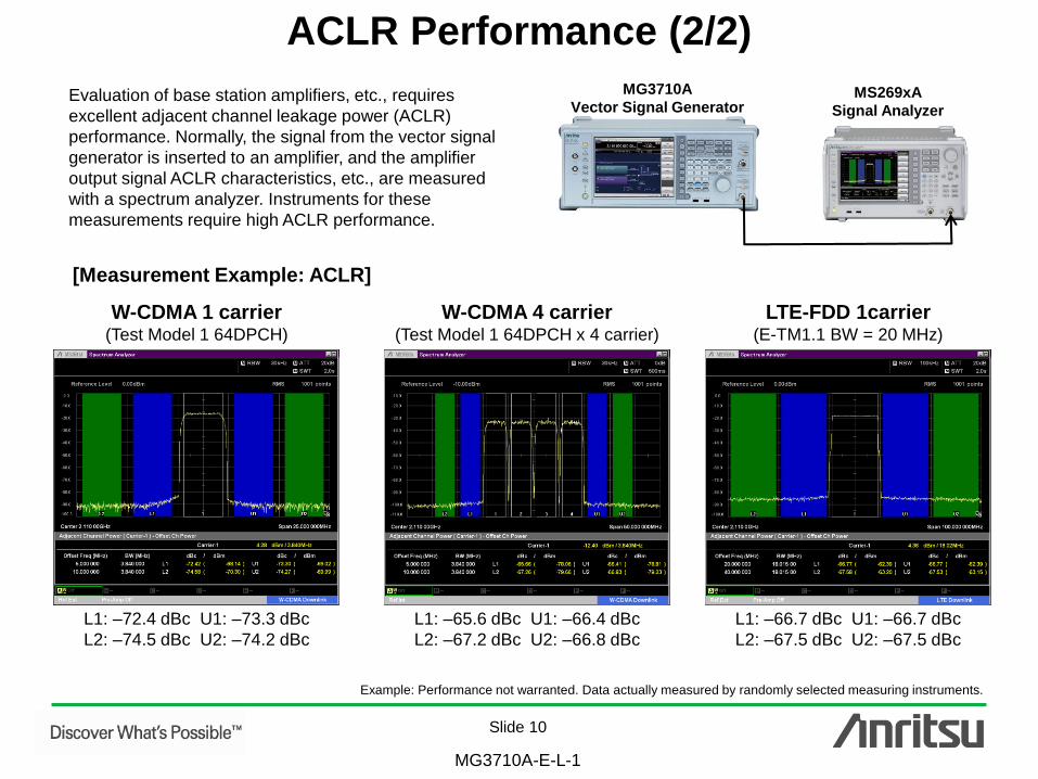
ACLR Performance (2/2)
W-CDMA 1 carrier (Test Model 1 64DPCH)
W-CDMA 4 carrier (Test Model 1 64DPCH x 4 carrier)
LTE-FDD 1carrier (E-TM1.1 BW = 20 MHz)
[Measurement Example: ACLR]
Evaluation of base station amplifiers, etc., requires
excellent adjacent channel leakage power (ACLR)
performance. Normally, the signal from the vector signal
generator is inserted to an amplifier, and the amplifier
output signal ACLR characteristics, etc., are measured
with a spectrum analyzer. Instruments for these
measurements require high ACLR performance.
L1: –72.4 dBc U1: –73.3 dBc
L2: –74.5 dBc U2: –74.2 dBc
L1: –65.6 dBc U1: –66.4 dBc
L2: –67.2 dBc U2: –66.8 dBc
L1: –66.7 dBc U1: –66.7 dBc
L2: –67.5 dBc U2: –67.5 dBc
MG3710A
Vector Signal Generator MS269xA
Signal Analyzer
Example: Performance not warranted. Data actually measured by randomly selected measuring instruments.
Slide 11
MG3710A-E-L-1
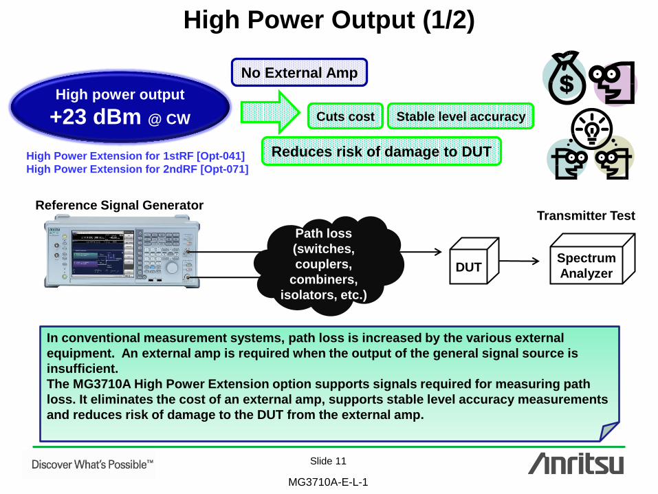
High Power Output (1/2)
In conventional measurement systems, path loss is increased by the various external
equipment. An external amp is required when the output of the general signal source is
insufficient.
The MG3710A High Power Extension option supports signals required for measuring path
loss. It eliminates the cost of an external amp, supports stable level accuracy measurements
and reduces risk of damage to the DUT from the external amp.
Spectrum
Analyzer DUT
Path loss
(switches,
couplers,
combiners,
isolators, etc.)
Cuts cost Stable level accuracy
Reduces risk of damage to DUT
No External Amp
Transmitter Test Reference Signal Generator
High power output
+23 dBm @ CW
High Power Extension for 1stRF [Opt-041]
High Power Extension for 2ndRF [Opt-071]

Slide 12
MG3710A-E-L-1
High Power Output (2/2)
Frequency Range Standard Opt-041/071
100 kHz ≤ f < 10 MHz +5 dBm +5 dBm
10 MHz ≤ f < 50 MHz +10 dBm +10 dBm
50 MHz ≤ f < 400 MHz
+13 dBm
+20 dBm
400 MHz ≤ f ≤ 3 GHz +23 dBm
3 GHz < f ≤ 4 GHz +20 dBm
4 GHz < f ≤ 5 GHz +13 dBm
5 GHz < f ≤ 6 GHz +11 dBm +11 dBm
Assured level accuracy at high levels (CW)
These options expand the MG3710A RF output
upper limit.
Generally, an external amplifier is used when
managing path losses occurring in measurement
systems as well as when the signal generator has
inadequate output power, such as when inputting
high-level modulation signals for evaluating amp
distortion. In these cases, not only must the
external amp output accuracy be assured, but it
must also be checked with a power meter each
time the frequency and level change. Moreover,
sometimes operating mistakes when using an
external amp can damage the device under test
(DUT). The MG3710A High Power Extension
options output the signal level required by the DUT
without requiring compensation for path losses. In
addition, the assured accuracy range supports
stable measurements. And finally, there is no risk
of unexpected damage to the DUT even when
used at the output setting limit.
High-Power Extension Option
High Power Extension for 1stRF [Opt-041]
High Power Extension for 2ndRF [Opt-071]
Slide 13
MG3710A-E-L-1
Low-Power Output
Reverse Input Power Protection
Level Setting Range
This option expands the MG3710A RF output lower
limit.
The lower limit of the standard level setting range
–110 dBm.
Adding this option expands the limit to –144 dBm.
Refer to the appended data sheet for the level
accuracy.
Low-Power Extension
Low Power Extension for 1stRF [Opt-042]
Low Power Extension for 2ndRF [Opt-072]
Setting Range [dBm]
Option without
Opt-043/073
with
Opt-043/073
Standard –110 to +17 –110 to +17
With Opt-041/071 –110 to +30 –110 to +25
With Opt-042/072 –144 to +17 –144 to +17
With Opt-041/071
& Opt-042/072 –144 to +30 –144 to +25
Reverse Input Power Protection
Reverse Power Protection for 1stRF [Opt-043]
Reverse Power Protection for 2ndRF [Opt-073]
This option protects the 1stRF and 2ndRF signal
output connector from reverse input power.
Maximum Reverse Input Power:
DC: 50 Vdc max.
AC: 20 W nom. (1 MHz < f ≤ 2 GHz)
10 W nom. (2 GHz < f ≤ 6 GHz)
Installing Opt-043/073 does not provide
100% assured protection against damage
from reverse input power, so take care not to
impress reverse input power whenever
possible.
Installing Opt-043/073 lowers ACLR
performance. Refer to the appended data
sheet for details.

Slide 14
MG3710A-E-L-1
Choice of Reference Oscillators
Rubidium Reference Oscillator [Opt-001]
High Stability Reference Oscillator [Opt-002]
Three reference oscillator options are supported. Select the High-Stability Reference Oscillator option
[Opt-002] when requiring high accuracy, depending on the measurement conditions; for even higher
accuracy, select the Rubidium Reference Oscillator option [Opt-001].
However, if external high-accuracy reference signals are available, selecting the standard reference
oscillator option helps reduce unnecessary costs.
Aging Rate 1 x 10⁻¹⁰/month
Temperature stability 2 x 10⁻⁹ (5 to 45C)
Start-up characteristics* 1 x 10⁻⁹ (7.5 minutes after power on)
*Compared to frequency after 24-h warm-up, at 23C
Pre-installed Reference Oscillator Aging Rate 1 x 10⁻⁷/day, 1 x 10⁻⁶/year
Temperature stability 2.5 x 10⁻⁶ (5 to 45C)
Aging Rate 1 x 10⁻⁸/day, 1 x 10⁻⁷/year
Temperature stability 2 x 10⁻⁸ (5 to 45C)
Start-up characteristics* 5 x 10⁻⁷ (2 minutes after power on)
5 x 10⁻⁸ (5 minutes after power on)
Slide 15
MG3710A-E-L-1
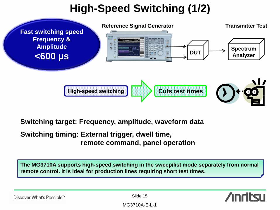
High-Speed Switching (1/2)
The MG3710A supports high-speed switching in the sweep/list mode separately from normal
remote control. It is ideal for production lines requiring short test times.
DUT Spectrum
Analyzer
High-speed switching Cuts test times
Switching target: Frequency, amplitude, waveform data
Switching timing: External trigger, dwell time,
remote command, panel operation
Reference Signal Generator Transmitter Test Fast switching speed
Frequency &
Amplitude
<600 µs
Slide 16
MG3710A-E-L-1
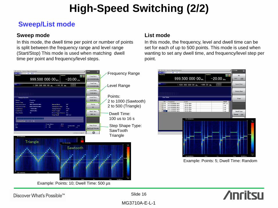
High-Speed Switching (2/2)
Sweep/List mode
Sweep mode
In this mode, the dwell time per point or number of points
is split between the frequency range and level range
(Start/Stop) This mode is used when matching dwell
time per point and frequency/level steps.
List mode
In this mode, the frequency, level and dwell time can be
set for each of up to 500 points. This mode is used when
wanting to set any dwell time, and frequency/level step per
point.
Frequency Range
Level Range
Points:
2 to 1000 (Sawtooth)
2 to 500 (Triangle)
Dwell Time:
100 us to 16 s
Step Shape Type:
SawTooth
Triangle
Triangle
Sawtooth
Example: Points: 10; Dwell Time: 500 µs
Example: Points: 5; Dwell Time: Random
Slide 17
MG3710A-E-L-1
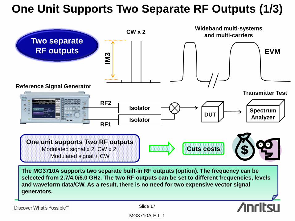
One Unit Supports Two Separate RF Outputs (1/3)
The MG3710A supports two separate built-in RF outputs (option). The frequency can be
selected from 2.7/4.0/6.0 GHz. The two RF outputs can be set to different frequencies, levels
and waveform data/CW. As a result, there is no need for two expensive vector signal
generators.
Two separate
RF outputs
Spectrum
Analyzer DUT
Isolator
Isolator RF1
RF2
One unit supports Two RF outputs Modulated signal x 2, CW x 2,
Modulated signal + CW
Cuts costs
IM3
CW x 2 Wideband multi-systems
and multi-carriers
EVM
Reference Signal Generator Transmitter Test

Slide 18
MG3710A-E-L-1
One Unit Supports Two Separate RF Outputs (2/3)
The MG3710A supports two separate built-in RF outputs (option). Each can output a different
frequency, level, and waveform data/CW and is ideal for Rx tests using two frequency offset
signals that cannot be set using the baseband combine function.
Two separate
RF outputs
DUT Isolator
Isolator RF1
RF2
Multi-system Rx
characteristics tests
Wanted
signal
Interference
signal
Cuts costs
Example: LTE + WLAN, LTE + Bluetooth, ISDB-T + WLAN, etc.
Receiver
Test
One unit supports Two RF outputs Wanted signal + Interference signal
Slide 19
MG3710A-E-L-1
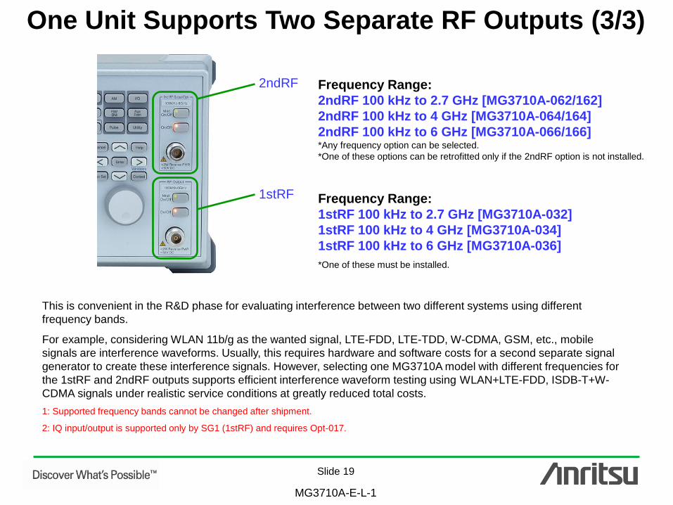
One Unit Supports Two Separate RF Outputs (3/3)
This is convenient in the R&D phase for evaluating interference between two different systems using different
frequency bands.
For example, considering WLAN 11b/g as the wanted signal, LTE-FDD, LTE-TDD, W-CDMA, GSM, etc., mobile
signals are interference waveforms. Usually, this requires hardware and software costs for a second separate signal
generator to create these interference signals. However, selecting one MG3710A model with different frequencies for
the 1stRF and 2ndRF outputs supports efficient interference waveform testing using WLAN+LTE-FDD, ISDB-T+W-
CDMA signals under realistic service conditions at greatly reduced total costs.
1: Supported frequency bands cannot be changed after shipment.
2: IQ input/output is supported only by SG1 (1stRF) and requires Opt-017.
2ndRF
1stRF
Frequency Range:
2ndRF 100 kHz to 2.7 GHz [MG3710A-062/162]
2ndRF 100 kHz to 4 GHz [MG3710A-064/164]
2ndRF 100 kHz to 6 GHz [MG3710A-066/166] *Any frequency option can be selected.
*One of these options can be retrofitted only if the 2ndRF option is not installed.
Frequency Range:
1stRF 100 kHz to 2.7 GHz [MG3710A-032]
1stRF 100 kHz to 4 GHz [MG3710A-034]
1stRF 100 kHz to 6 GHz [MG3710A-036]
*One of these must be installed.
Slide 20
MG3710A-E-L-1
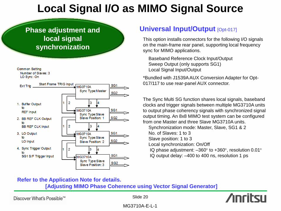
Local Signal I/O as MIMO Signal Source
This option installs connectors for the following I/O signals
on the main-frame rear panel, supporting local frequency
sync for MIMO applications.
Baseband Reference Clock Input/Output
Sweep Output (only supports SG1)
Local Signal Input/Output
*Bundled with J1539A AUX Conversion Adapter for Opt-
017/117 to use rear-panel AUX connector.
The Sync Multi SG function shares local signals, baseband
clocks and trigger signals between multiple MG3710A units
to output phase coherency signals with synchronized signal
output timing. An 8x8 MIMO test system can be configured
from one Master and three Slave MG3710A units.
Synchronization mode: Master, Slave, SG1 & 2
No. of Slaves: 1 to 3
Slave position: 1 to 3
Local synchronization: On/Off
IQ phase adjustment: –360 to +360, resolution 0.01
IQ output delay: –400 to 400 ns, resolution 1 ps
Phase adjustment and
local signal
synchronization
Refer to the Application Note for details.
[Adjusting MIMO Phase Coherence using Vector Signal Generator]
Universal Input/Output [Opt-017]

Slide 21
MG3710A-E-L-1
One RF Outputs Wanted + Interference Signals (1/6)
The MG3710A has two waveform memories for each RF output for setting and outputting
different waveform data. One RF outputs the combined wanted + interference signals for the
baseband bandwidth.
Wanted Signal + Interference Signal
at One RF Output Receiver
Test DUT
Outputs two signals at one RF
(Baseband Signal Combine function)
Adjacent
Channel
Selectivity, etc. Wanted
signal
Interference signal
Baseband bandwidth
Combination of Baseband Signal function:
Waveform data = 2 patterns (dual memory);
modulated signal x 2, CW x 2, modulated signal + CW, etc.
Setting: Frequency offset, level offset, delay time
Frequency offset range: < baseband bandwidth (60 MHz max.)
One RF outputs
Wanted + Interference signals Cuts costs

Slide 22
MG3710A-E-L-1
One RF Outputs Wanted + Interference Signals (2/6)
Level Setting
Frequency Offset Setting Range
Setting Range: –80 to +80 MHz
Resolution: 1 Hz
Time offset
Setting Range
CW Selection
A: Pattern A center
B: Pattern B center
Baseband DC:
Centered at baseband DC
position
Waveform
pattern A
Example:
Wanted Signal
Waveform
pattern B
Example:
Interference Signal,
Delay Signal
Setting Range:
0 ~ pattern B sampling
data count – 1
Setting Range: –80 to +80 dB
Resolution: 0.01 dB
Combination of Baseband Signal Example
Combination of Baseband Signal Function
Combination of Baseband Signal for 1stRF [Opt-048]
Combination of Baseband Signal for 2ndRF [Opt-078] The Combination of Baseband Signal option installs two
waveform memories for either the 1stRF (or 2ndRF) SG to
combine two waveform patterns as the baseband for output,
eliminating the need for two separate and expensive vector
signal generators.
Slide 23
MG3710A-E-L-1
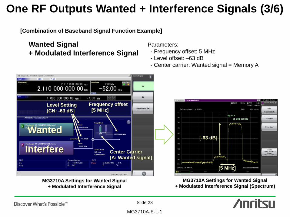
One RF Outputs Wanted + Interference Signals (3/6)
MG3710A Settings for Wanted Signal
+ Modulated Interference Signal
MG3710A Settings for Wanted Signal
+ Modulated Interference Signal (Spectrum)
[Combination of Baseband Signal Function Example]
Level Setting
[CN: -63 dB]
Wanted
Interfere
Frequency offset
[5 MHz]
Center Carrier
[A: Wanted signal]
[5 MHz]
[-63 dB]
Parameters:
- Frequency offset: 5 MHz
- Level offset: –63 dB
- Center carrier: Wanted signal = Memory A
Wanted Signal
+ Modulated Interference Signal

Slide 24
MG3710A-E-L-1
One RF Outputs Wanted + Interference Signals (4/6)
[Combination of Baseband Signal Function Example]
MG3710A Settings for
Wanted Signal + Delayed Signal
Wanted Signal + Delayed Signal
(Delay Profile)
Level Setting
[CN: 15 dB]
Wanted
Delayed Time offset
30 us
-15 dB
Delay Time
Parameters:
- Frequency offset: 0 Hz
- Level offset: 15 dB
- Time offset (Delay): 30 µs
Wanted Signal
+ Delayed Signal
Slide 25
MG3710A-E-L-1
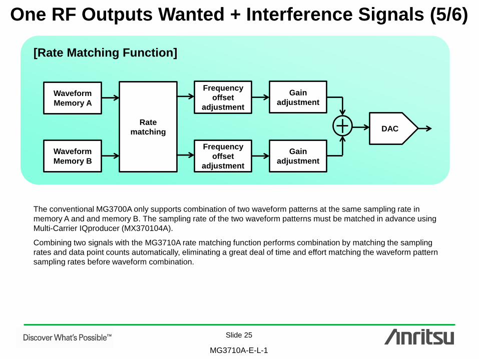
One RF Outputs Wanted + Interference Signals (5/6)
[Rate Matching Function]
Waveform
Memory A
DAC
Waveform
Memory B
Gain
adjustment
Frequency
offset
adjustment
Rate
matching
Gain
adjustment
Frequency
offset
adjustment
The conventional MG3700A only supports combination of two waveform patterns at the same sampling rate in
memory A and and memory B. The sampling rate of the two waveform patterns must be matched in advance using
Multi-Carrier IQproducer (MX370104A).
Combining two signals with the MG3710A rate matching function performs combination by matching the sampling
rates and data point counts automatically, eliminating a great deal of time and effort matching the waveform pattern
sampling rates before waveform combination.
Slide 26
MG3710A-E-L-1
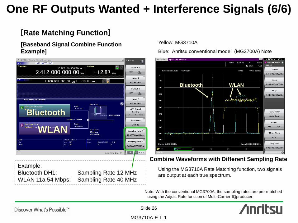
One RF Outputs Wanted + Interference Signals (6/6)
[Baseband Signal Combine Function
Example]
[Rate Matching Function]
Example:
Bluetooth DH1: Sampling Rate 12 MHz
WLAN 11a 54 Mbps: Sampling Rate 40 MHz
Bluetooth
WLAN
Bluetooth WLAN
Yellow: MG3710A
Blue: Anritsu conventional model (MG3700A) Note
Combine Waveforms with Different Sampling Rate
Using the MG3710A Rate Matching function, two signals
are output at each true spectrum.
Note: With the conventional MG3700A, the sampling rates are pre-matched
using the Adjust Rate function of Multi-Carrier IQproducer.

Slide 27
MG3710A-E-L-1
One RF Outputs Wanted + AWGN Signals (1/2)
Noise Bandwidth
Carrier Level
Waveform
pattern A
Example:
Wanted Signal
AWGN Generator
AWGN Flat Bandwidth part
Sets change target when setting C/N Ratio
Carrier: Changes carrier (fixed AWGN)
Noise: Changes AWGN (fixed carrier)
Constant: Fixes output level and change
carrier and AWGN
Setting Range: –40 to +40 dB
Resolution: 0.01 dB
Example of AWGN Generator
AWGN Generator
AWGN for 1stRF [Opt-049]
AWGN for 2ndRF [Opt-079]
This option adds internally generated AWGN to wanted signals. The
On/Off button switches the AWGN output.
When there is no carrier, only AWGN is output (ARB = Off).
Noise (AWGN) Level
Carrier/Noise Ratio
C/N Set Signal
Select AWGN On/Off
(Enabled when no wanted signal)
Built-in AWGN
Generator

Slide 28
MG3710A-E-L-1
One RF Outputs Wanted + AWGN Signals (2/2)
Example: Wanted Signal + AWGN Example: AWGN only
Wanted
AWGN AWGN Level of AWGN -15 dBm -20 dBm
When adding AWGN to the wanted signal, Noise Level on
the screen displays the noise level in the wanted signal
band.
ARB=Off
ARB=Off ARB=On
ARB=On
When outputting only AWGN, Noise Level on the screen
displays the set noise bandwidth level. In the above setting
example, it is the power in the 7.68-MHz band.
Total Level
–35 dBm
Level of
wanted signal
Level of AWGN
Total Level
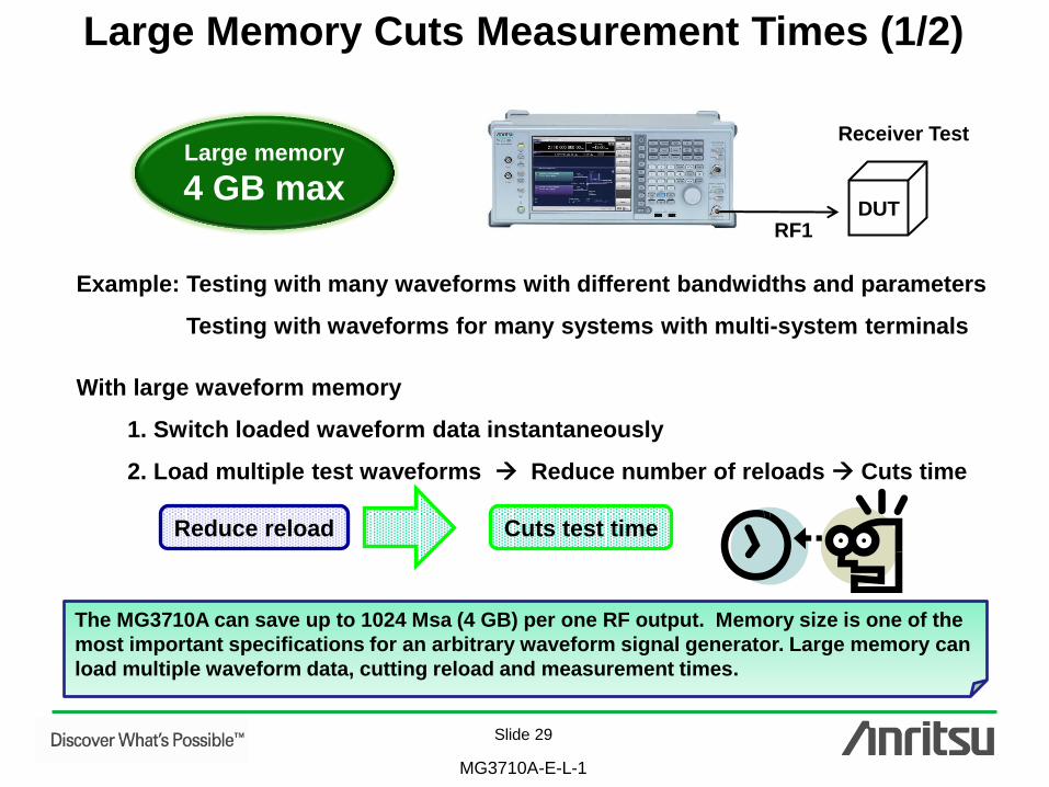
Slide 29
MG3710A-E-L-1
Large Memory Cuts Measurement Times (1/2)
The MG3710A can save up to 1024 Msa (4 GB) per one RF output. Memory size is one of the
most important specifications for an arbitrary waveform signal generator. Large memory can
load multiple waveform data, cutting reload and measurement times.
DUT RF1
Example: Testing with many waveforms with different bandwidths and parameters
Testing with waveforms for many systems with multi-system terminals
With large waveform memory
1. Switch loaded waveform data instantaneously
2. Load multiple test waveforms Reduce number of reloads Cuts time
Reduce reload Cuts test time
Large memory
4 GB max
Receiver Test
Slide 30
MG3710A-E-L-1
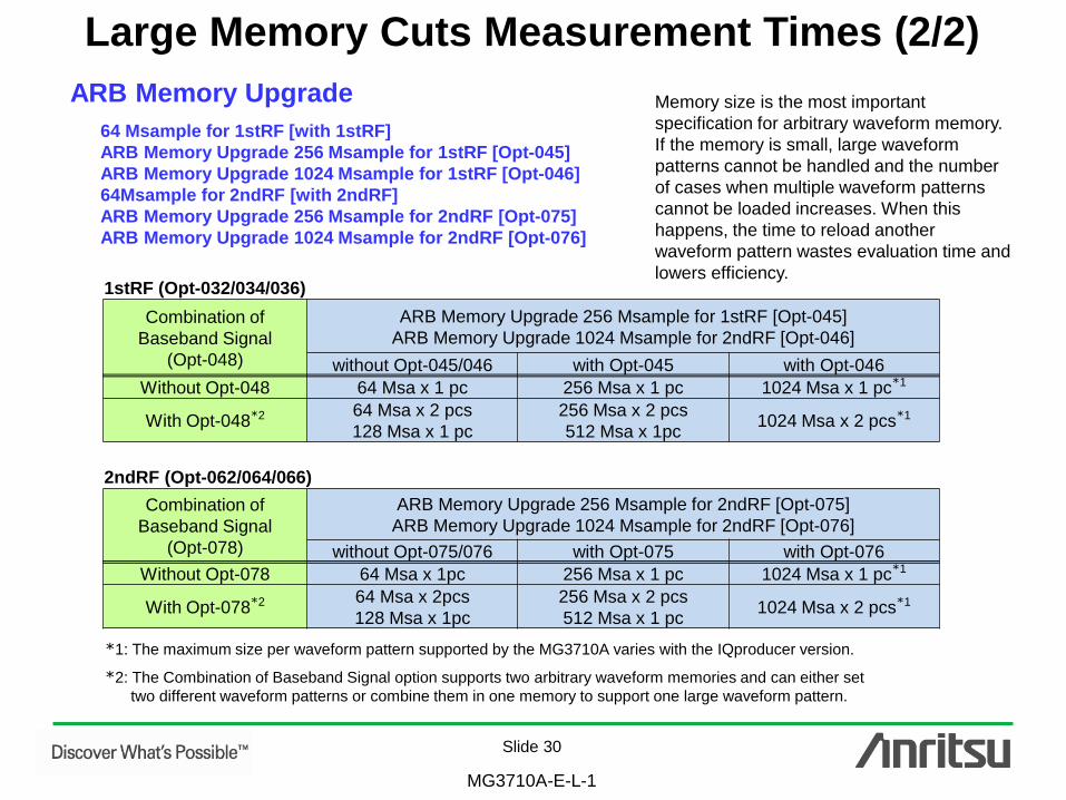
Large Memory Cuts Measurement Times (2/2)
1stRF (Opt-032/034/036)
Combination of
Baseband Signal
(Opt-048)
ARB Memory Upgrade 256 Msample for 1stRF [Opt-045]
ARB Memory Upgrade 1024 Msample for 2ndRF [Opt-046]
without Opt-045/046 with Opt-045 with Opt-046
Without Opt-048 64 Msa x 1 pc 256 Msa x 1 pc 1024 Msa x 1 pc*1
With Opt-048*2 64 Msa x 2 pcs
128 Msa x 1 pc
256 Msa x 2 pcs
512 Msa x 1pc 1024 Msa x 2 pcs*1
2ndRF (Opt-062/064/066)
Combination of
Baseband Signal
(Opt-078)
ARB Memory Upgrade 256 Msample for 2ndRF [Opt-075]
ARB Memory Upgrade 1024 Msample for 2ndRF [Opt-076]
without Opt-075/076 with Opt-075 with Opt-076
Without Opt-078 64 Msa x 1pc 256 Msa x 1 pc 1024 Msa x 1 pc*1
With Opt-078*2 64 Msa x 2pcs
128 Msa x 1pc
256 Msa x 2 pcs
512 Msa x 1 pc 1024 Msa x 2 pcs*1
*1: The maximum size per waveform pattern supported by the MG3710A varies with the IQproducer version.
*2: The Combination of Baseband Signal option supports two arbitrary waveform memories and can either set
two different waveform patterns or combine them in one memory to support one large waveform pattern.
Memory size is the most important
specification for arbitrary waveform memory.
If the memory is small, large waveform
patterns cannot be handled and the number
of cases when multiple waveform patterns
cannot be loaded increases. When this
happens, the time to reload another
waveform pattern wastes evaluation time and
lowers efficiency.
ARB Memory Upgrade
64 Msample for 1stRF [with 1stRF]
ARB Memory Upgrade 256 Msample for 1stRF [Opt-045]
ARB Memory Upgrade 1024 Msample for 1stRF [Opt-046]
64Msample for 2ndRF [with 2ndRF]
ARB Memory Upgrade 256 Msample for 2ndRF [Opt-075]
ARB Memory Upgrade 1024 Msample for 2ndRF [Opt-076]
Slide 31
MG3710A-E-L-1
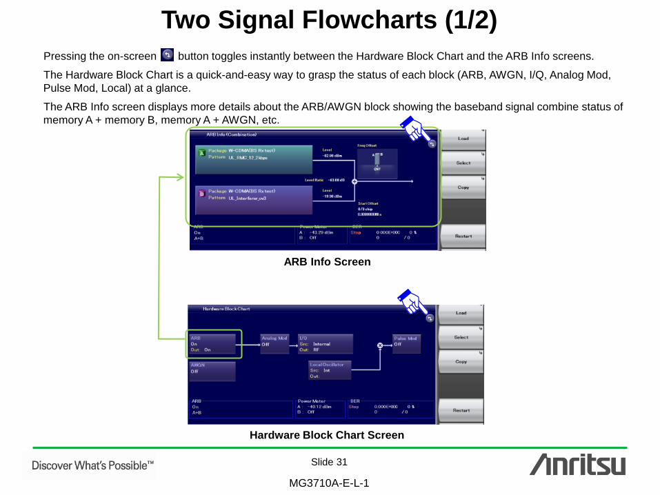
Two Signal Flowcharts (1/2)
Pressing the on-screen button toggles instantly between the Hardware Block Chart and the ARB Info screens.
The Hardware Block Chart is a quick-and-easy way to grasp the status of each block (ARB, AWGN, I/Q, Analog Mod,
Pulse Mod, Local) at a glance.
The ARB Info screen displays more details about the ARB/AWGN block showing the baseband signal combine status of
memory A + memory B, memory A + AWGN, etc.
ARB Info Screen
Hardware Block Chart Screen

Slide 32
MG3710A-E-L-1
Two Signal Flowcharts (2/2)
Hardware Block Chart (explanation)
Hardware Block Chart Display Contents (explanation)
Slide 33
MG3710A-E-L-1
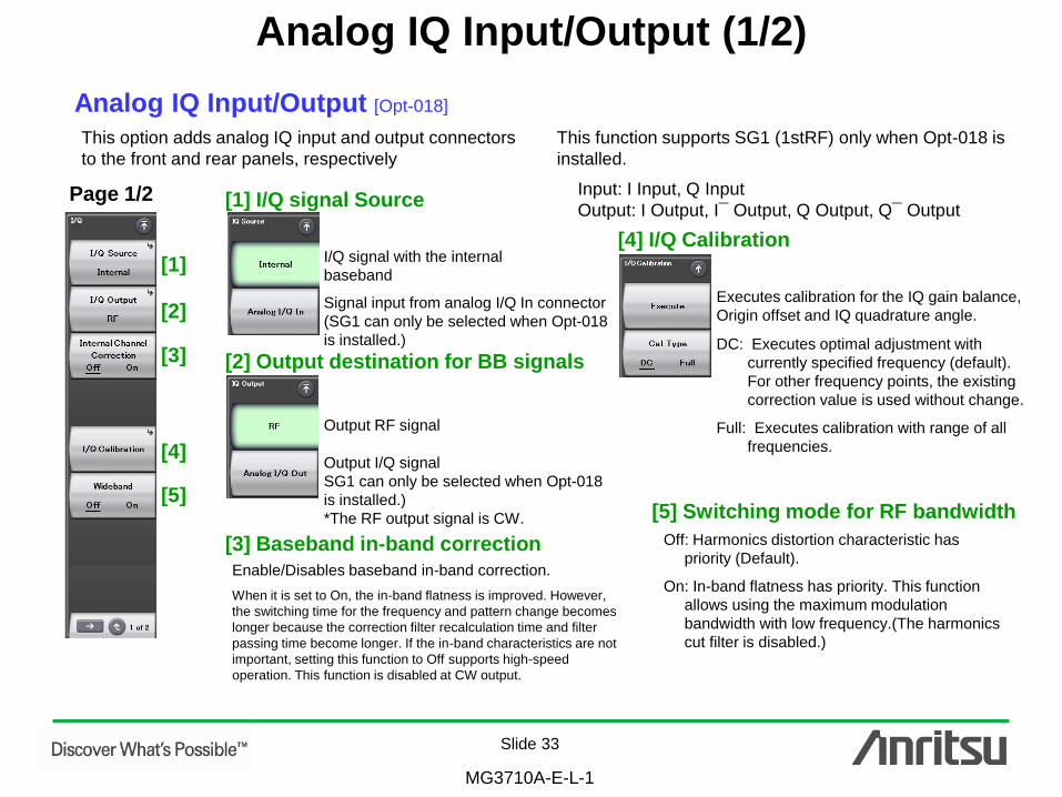
Analog IQ Input/Output (1/2)
This option adds analog IQ input and output connectors
to the front and rear panels, respectively
[1]
[2]
[3]
[4]
[5]
[1] I/Q signal Source
[2] Output destination for BB signals
I/Q signal with the internal
baseband
Signal input from analog I/Q In connector
(SG1 can only be selected when Opt-018
is installed.)
Output RF signal
Output I/Q signal
SG1 can only be selected when Opt-018
is installed.)
*The RF output signal is CW.
[3] Baseband in-band correction
Enable/Disables baseband in-band correction.
When it is set to On, the in-band flatness is improved. However,
the switching time for the frequency and pattern change becomes
longer because the correction filter recalculation time and filter
passing time become longer. If the in-band characteristics are not
important, setting this function to Off supports high-speed
operation. This function is disabled at CW output.
[4] I/Q Calibration
Executes calibration for the IQ gain balance,
Origin offset and IQ quadrature angle.
DC: Executes optimal adjustment with
currently specified frequency (default).
For other frequency points, the existing
correction value is used without change.
Full: Executes calibration with range of all
frequencies.
[5] Switching mode for RF bandwidth
Off: Harmonics distortion characteristic has
priority (Default).
On: In-band flatness has priority. This function
allows using the maximum modulation
bandwidth with low frequency.(The harmonics
cut filter is disabled.)
Page 1/2
Analog IQ Input/Output [Opt-018]
This function supports SG1 (1stRF) only when Opt-018 is
installed.
Input: I Input, Q Input
Output: I Output, I¯ Output, Q Output, Q¯ Output
Slide 34
MG3710A-E-L-1
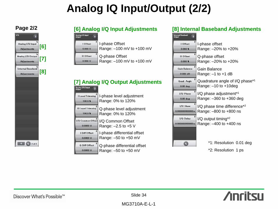
Analog IQ Input/Output (2/2)
[6]
Page 2/2
[7]
[8]
[6] Analog I/Q Input Adjustments
[7] Analog I/Q Output Adjustments
[8] Internal Baseband Adjustments
I-phase Offset
Range: –100 mV to +100 mV
Q-phase Offset
Range: –100 mV to +100 mV
I-phase level adjustment
Range: 0% to 120%
Q-phase level adjustment
Range: 0% to 120%
I/Q Common Offset
Range: –2.5 to +5 V
I-phase differential offset
Range: –50 to +50 mV
Q-phase differential offset
Range: –50 to +50 mV
I-phase offset
Range: –20% to +20%
Q-phase offset
Range: –20% to +20%
Gain Balance
Range: –1 to +1 dB
Quadrature angle of I/Q phase*1
Range: –10 to +10deg
I/Q phase adjustment*1
Range: –360 to +360 deg
I/Q phase time difference*2
Range: –800 to +800 ns
I/Q output timing*2
Range: –400 to +400 ns
*1: Resolution 0.01 deg
*2: Resolution 1 ps
Slide 35
MG3710A-E-L-1
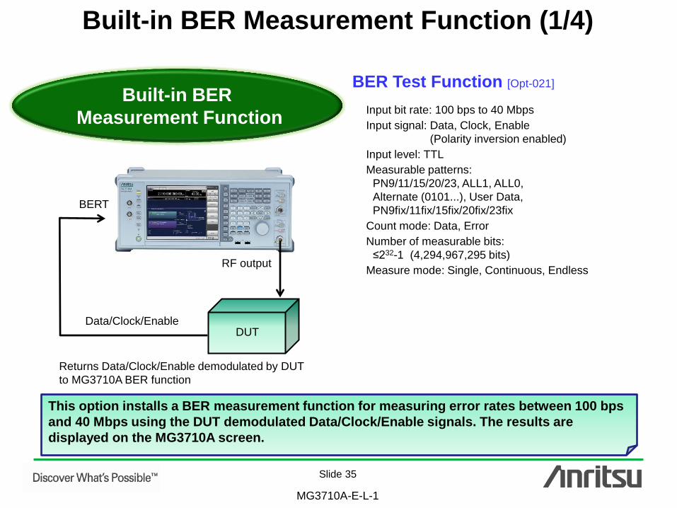
Built-in BER Measurement Function (1/4)
This option installs a BER measurement function for measuring error rates between 100 bps
and 40 Mbps using the DUT demodulated Data/Clock/Enable signals. The results are
displayed on the MG3710A screen.
DUT
RF output
Data/Clock/Enable
Returns Data/Clock/Enable demodulated by DUT
to MG3710A BER function
Input bit rate: 100 bps to 40 Mbps
Input signal: Data, Clock, Enable
(Polarity inversion enabled)
Input level: TTL
Measurable patterns:
PN9/11/15/20/23, ALL1, ALL0,
Alternate (0101...), User Data,
PN9fix/11fix/15fix/20fix/23fix
Count mode: Data, Error
Number of measurable bits:
≤232-1 (4,294,967,295 bits)
Measure mode: Single, Continuous, Endless
BER Test Function [Opt-021]
Built-in BER
Measurement Function
BERT
Slide 36
MG3710A-E-L-1
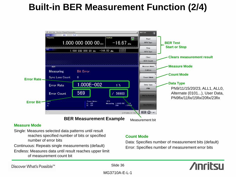
Built-in BER Measurement Function (2/4)
Clears measurement result
Error Rate
Error Bit
BER Measurement Example
Measure Mode
Count Mode
Data Type
BER Test
Start or Stop
Data: Specifies number of measurement bits (default)
Error: Specifies number of measurement error bits
PN9/11/15/20/23, ALL1, ALL0,
Alternate (0101...), User Data,
PN9fix/11fix/15fix/20fix/23fix
Single: Measures selected data patterns until result
reaches specified number of bits or specified
number of error bits
Continuous: Repeats single measurements (default)
Endless: Measures data until result reaches upper limit
of measurement count bit
Measurement bit
Measure Mode
Count Mode

Slide 37
MG3710A-E-L-1
Built-in BER Measurement Function (3/4)
At BER measurement, special PN patterns
called PN_Fix patterns can be used. A PN Fix
pattern consists of repeated parts of PN
patterns, and PN patterns with a shorter
length than 1 cycle.
Even when the PN data part of the waveform
pattern output from the MG3710A has no
periodicity, BER measurement is supported
by selecting PN Fix at the BER measurement
function.
[PN Fix pattern]
Setting Range:
96 to 134217728 bit (0 x 8000000)
Resolution: 1 bit
Initial Pattern Pattern Length
Slide 38
MG3710A-E-L-1
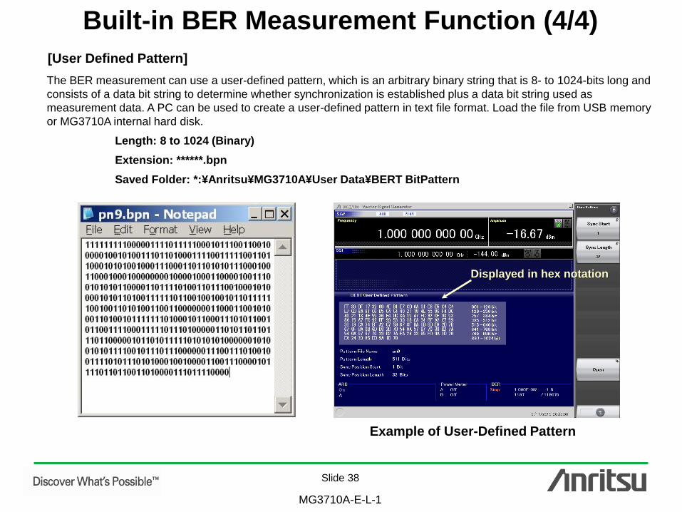
Built-in BER Measurement Function (4/4)
The BER measurement can use a user-defined pattern, which is an arbitrary binary string that is 8- to 1024-bits long and
consists of a data bit string to determine whether synchronization is established plus a data bit string used as
measurement data. A PC can be used to create a user-defined pattern in text file format. Load the file from USB memory
or MG3710A internal hard disk.
Length: 8 to 1024 (Binary)
Extension: ******.bpn
Saved Folder: *:¥Anritsu¥MG3710A¥User Data¥BERT BitPattern
[User Defined Pattern]
Example of User-Defined Pattern
Displayed in hex notation

Slide 39
MG3710A-E-L-1
Supports Two USB Type Power Sensor (1/4)
Up to two USB power sensors can be
connected to the MG3710A to display the
measurement results on the MG3710A
screen.
USB Power Sensor [Sold Separately]
Supports two USB
power sensors max.
DUT
USB Connection
Example:
MA24106
Level Offset: –100 to +100 dB
Average: 1 to 2048
Unit: dBm, W
COM Port: 2 to 8
Power Meter Measurement Screen
*: MA24104A has been discontinued.
Replacement model is MA24105A.
Slide 40
MG3710A-E-L-1
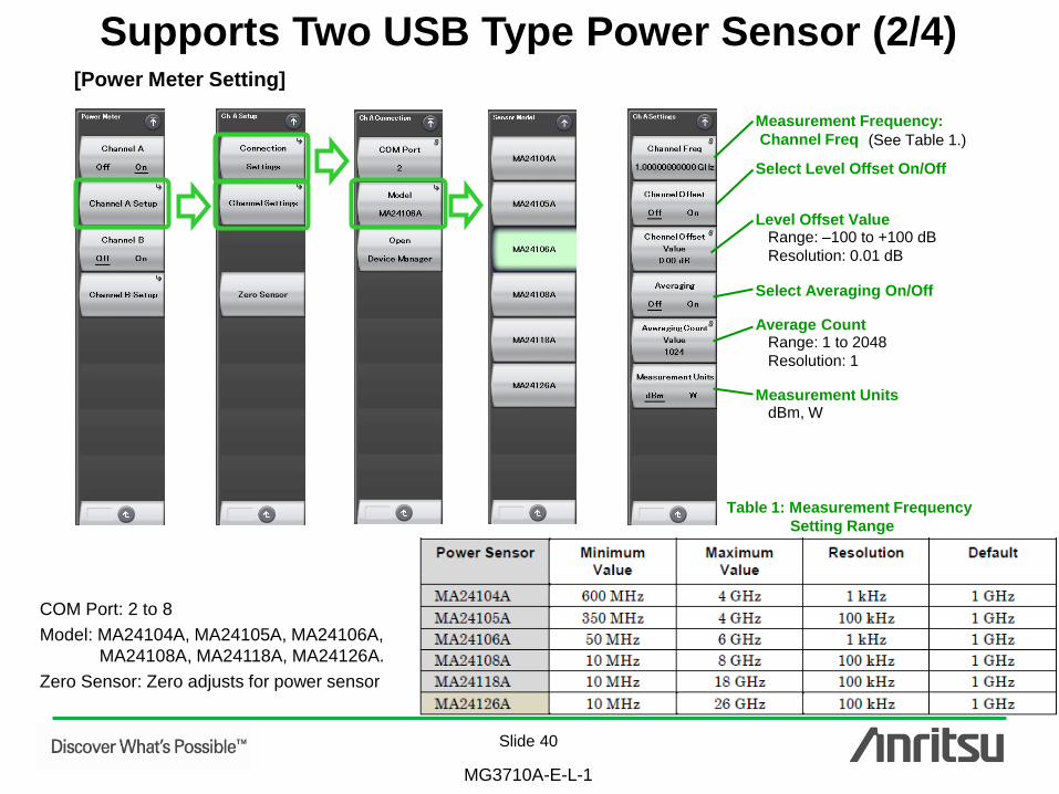
[Power Meter Setting]
COM Port: 2 to 8
Model: MA24104A, MA24105A, MA24106A,
MA24108A, MA24118A, MA24126A.
Zero Sensor: Zero adjusts for power sensor
Measurement Frequency:
Channel Freq (See Table 1.)
Select Level Offset On/Off
Level Offset Value Range: –100 to +100 dB
Resolution: 0.01 dB
Select Averaging On/Off
Average Count Range: 1 to 2048
Resolution: 1
Measurement Units dBm, W
Table 1: Measurement Frequency
Setting Range
Supports Two USB Type Power Sensor (2/4)

Slide 41
MG3710A-E-L-1
[Checking Com Port]
1. Display Windows Device Manager
[F2: Channel A Setup] or [F4: Channel B Setup]
> [F1: Connection Settings]
> [F3: Open Device Manager]
2. Check Ports (COM & LPT)
Supports Two USB Type Power Sensor (3/4)
Slide 42
MG3710A-E-L-1
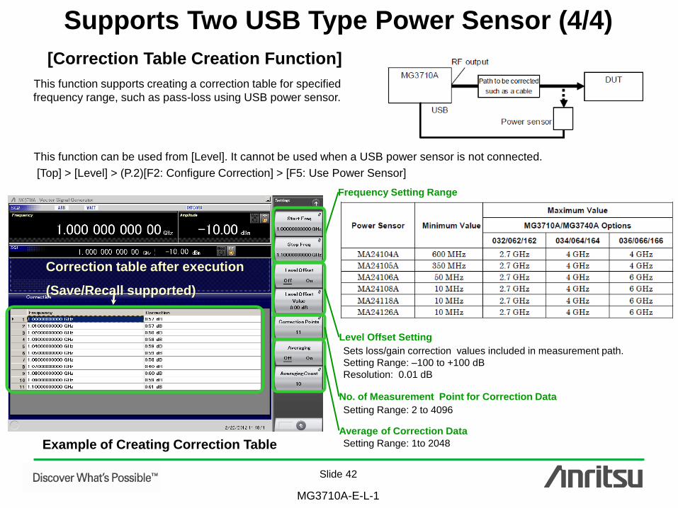
[Correction Table Creation Function]
Frequency Setting Range
Sets loss/gain correction values included in measurement path.
Setting Range: –100 to +100 dB
Resolution: 0.01 dB
Example of Creating Correction Table
This function supports creating a correction table for specified
frequency range, such as pass-loss using USB power sensor.
Level Offset Setting
No. of Measurement Point for Correction Data
Setting Range: 2 to 4096
Average of Correction Data
Setting Range: 1to 2048
This function can be used from [Level]. It cannot be used when a USB power sensor is not connected.
[Top] > [Level] > (P.2)[F2: Configure Correction] > [F5: Use Power Sensor]
Correction table after execution
(Save/Recall supported)
Supports Two USB Type Power Sensor (4/4)
Slide 43
MG3710A-E-L-1
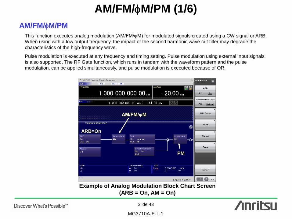
AM/FM/M/PM (1/6)
This function executes analog modulation (AM/FM/φM) for modulated signals created using a CW signal or ARB.
When using with a low output frequency, the impact of the second harmonic wave cut filter may degrade the
characteristics of the high-frequency wave.
Pulse modulation is executed at any frequency and timing setting. Pulse modulation using external input signals
is also supported. The RF Gate function, which runs in tandem with the waveform pattern and the pulse
modulation, can be applied simultaneously, and pulse modulation is executed because of OR.
AM/FM/M/PM
PM
AM/FM/φM
ARB=On
Example of Analog Modulation Block Chart Screen
(ARB = On, AM = On)

Slide 44
MG3710A-E-L-1
AM/FM/M/PM (2/6)
Adding additional analog modulation input options (Opt.050/080) extends to two internal modulation sources
(AM/FM/ΦM) and one external modulation source supporting simultaneous two-signal modulation.
• AM + FM
• AM + φM
• Internal 1 + Internal 2
• Internal + External
* FM + φM does not support.
Additional Analog Modulation Input [Opt.050/080]

Slide 45
MG3710A-E-L-1
AM/FM/M/PM (3/6)
Select AM Modulation Scale
AM Depth (Lin):
Lin: Linear format
Exp: Exponential format (Log)
Range: 0.1 Hz to 50 MHz
Resolution: 0.1 Hz
AM Depth (Log):
AM Rate:
Select AM On/Off
Range: 0 to 10 dB
Resolution: 0.1 dB
AM Setting Screen
Range: 0% to 100%
Resolution: 0.1%
AM Setting Screen
AM Image (Lin) AM Image (Log)
Slide 46
MG3710A-E-L-1
AM/FM/M/PM (4/6)
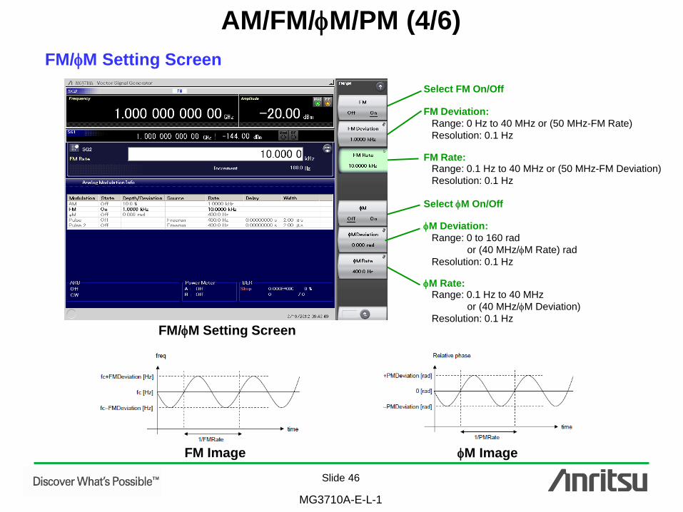
FM/M Setting Screen
FM Deviation:
FM Rate:
Range: 0 Hz to 40 MHz or (50 MHz-FM Rate)
Resolution: 0.1 Hz
Select FM On/Off
Range: 0.1 Hz to 40 MHz or (50 MHz-FM Deviation)
Resolution: 0.1 Hz
M Deviation:
M Rate:
Range: 0 to 160 rad
or (40 MHz/M Rate) rad
Resolution: 0.1 Hz
Select M On/Off
Range: 0.1 Hz to 40 MHz
or (40 MHz/M Deviation)
Resolution: 0.1 Hz
FM/M Setting Screen
FM Image M Image

Slide 47
MG3710A-E-L-1
AM/FM/M/PM (5/6)
PM Setting Screen
Pulse Source:
Pulse Rate:
Select PM On/Off
Range: 0.1 Hz to 10 MHz
Resolution: 0.1 Hz
Pulse Period: Range: 10 ns to 20 s
Resolution: 10 ns
Pulse Delay from trigger: Range: 0 to 20s – Pulse Width
Resolution: 10 ns
Pulse Width: Range: 10 ns to Pulse Period*1
10 ns to 20 s – Pulse Delay*2
Resolution: 10 ns
Delay time from first to second Pulse:
Pulse 2 Delay
Range: 0s to 20s – Pulse 2 Width – Pulse Delay
Resolution: 10ns
Second pulse width: Pulse 2 Width Range: 10 ns to 20 s – Pulse 2 Delay – Pulse Delay
Resolution: 10 ns
*1: When Pulse Source is [Free run] or [Gated]
*2: When Pulse Source is [Triggered], [Adjustable], [Doublet] or [Trigger Doublet].
(See next slide.)

Slide 48
MG3710A-E-L-1
AM/FM/M/PM (6/6)
PM: Pulse Source
Square
Freerun
Adjustable Doublet
Trigger Doublet
Gated
Ext Pulse
Triggered
Slide 49
MG3710A-E-L-1
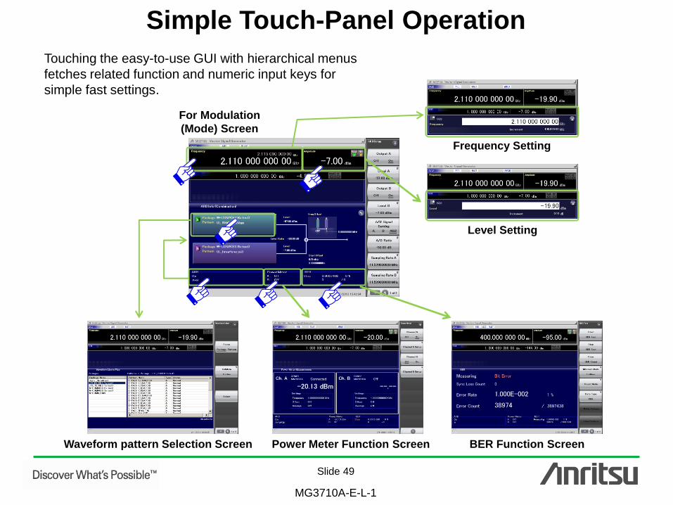
Simple Touch-Panel Operation
Touching the easy-to-use GUI with hierarchical menus
fetches related function and numeric input keys for
simple fast settings.
BER Function Screen Power Meter Function Screen Waveform pattern Selection Screen
For Modulation
(Mode) Screen
Frequency Setting
Level Setting
Slide 50
MG3710A-E-L-1
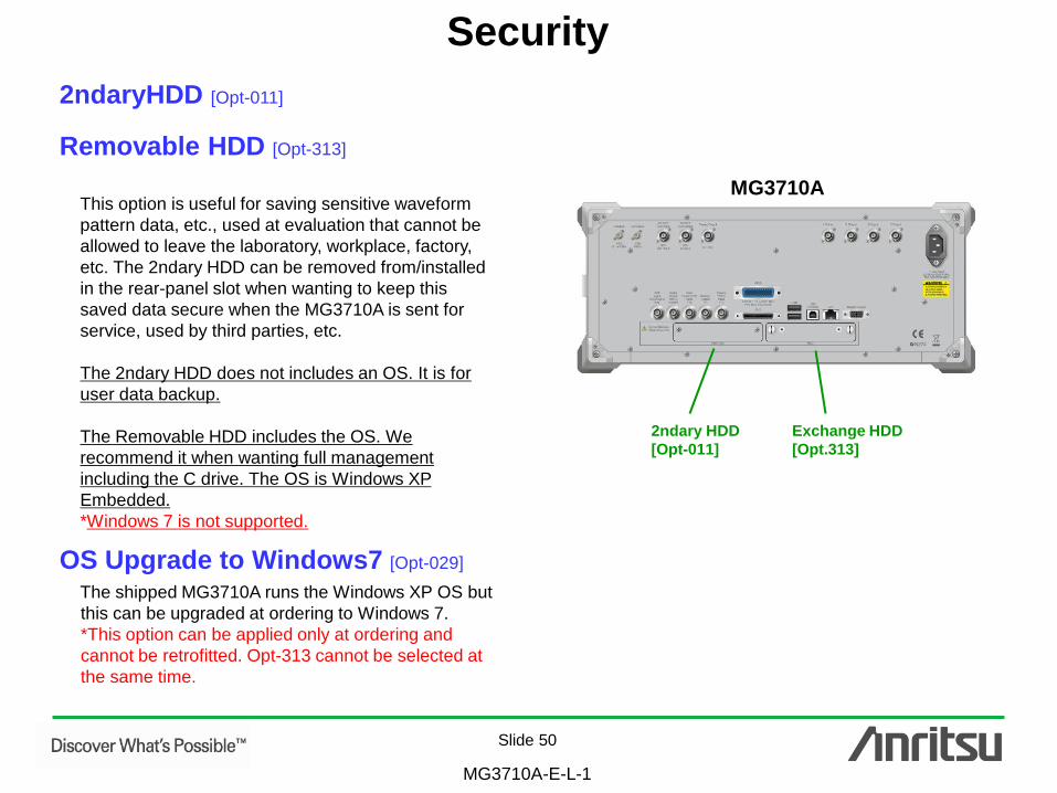
Security
This option is useful for saving sensitive waveform
pattern data, etc., used at evaluation that cannot be
allowed to leave the laboratory, workplace, factory,
etc. The 2ndary HDD can be removed from/installed
in the rear-panel slot when wanting to keep this
saved data secure when the MG3710A is sent for
service, used by third parties, etc.
The 2ndary HDD does not includes an OS. It is for
user data backup.
The Removable HDD includes the OS. We
recommend it when wanting full management
including the C drive. The OS is Windows XP
Embedded.
*Windows 7 is not supported.
2ndaryHDD [Opt-011]
Removable HDD [Opt-313]
MG3710A
2ndary HDD
[Opt-011]
Exchange HDD
[Opt.313]
OS Upgrade to Windows7 [Opt-029]
The shipped MG3710A runs the Windows XP OS but
this can be upgraded at ordering to Windows 7.
*This option can be applied only at ordering and
cannot be retrofitted. Opt-313 cannot be selected at
the same time.
Slide 51
MG3710A-E-L-1
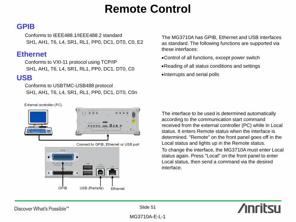
Remote Control
GPIB
Ethernet
USB
The MG3710A has GPIB, Ethernet and USB interfaces
as standard. The following functions are supported via
these interfaces:
Control of all functions, except power switch
Reading of all status conditions and settings
Interrupts and serial polls
Conforms to IEEE488.1/IEEE488.2 standard
SH1, AH1, T6, L4, SR1, RL1, PP0, DC1, DT0, C0, E2
Conforms to USBTMC-USB488 protocol
SH1, AH1, T6, L4, SR1, RL1, PP0, DC1, DT0, C0n
Conforms to VXI-11 protocol using TCP/IP
SH1, AH1, T6, L4, SR1, RL1, PP0, DC1, DT0, C0
The interface to be used is determined automatically
according to the communication start command
received from the external controller (PC) while in Local
status. It enters Remote status when the interface is
determined. "Remote" on the front panel goes off in the
Local status and lights up in the Remote status.
To change the interface, the MG3710A must enter Local
status again. Press "Local" on the front panel to enter
Local status, then send a command via the desired
interface.

Slide 52
MG3710A-E-L-1
MG3710A Vector Signal Generator
Waveform Generation Software
IQproducer Introduction
Some of these functions require a separate charged license.
Slide 53
MG3710A-E-L-1
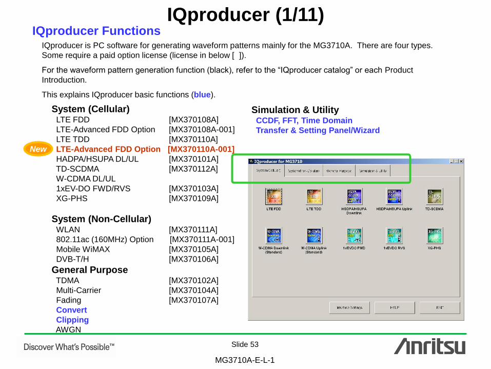
IQproducer (1/11)
IQproducer is PC software for generating waveform patterns mainly for the MG3710A. There are four types.
Some require a paid option license (license in below [ ]).
For the waveform pattern generation function (black), refer to the “IQproducer catalog” or each Product
Introduction.
This explains IQproducer basic functions (blue).
System (Cellular) LTE FDD [MX370108A]
LTE-Advanced FDD Option [MX370108A-001]
LTE TDD [MX370110A]
LTE-Advanced FDD Option [MX370110A-001]
HADPA/HSUPA DL/UL [MX370101A]
TD-SCDMA [MX370112A]
W-CDMA DL/UL
1xEV-DO FWD/RVS [MX370103A]
XG-PHS [MX370109A]
System (Non-Cellular) WLAN [MX370111A]
802.11ac (160MHz) Option [MX370111A-001]
Mobile WiMAX [MX370105A]
DVB-T/H [MX370106A]
General Purpose TDMA [MX370102A]
Multi-Carrier [MX370104A]
Fading [MX370107A]
Convert
Clipping
AWGN
Simulation & Utility CCDF, FFT, Time Domain
Transfer & Setting Panel/Wizard
IQproducer Functions
New
Slide 54
MG3710A-E-L-1
IQproducer (2/11)
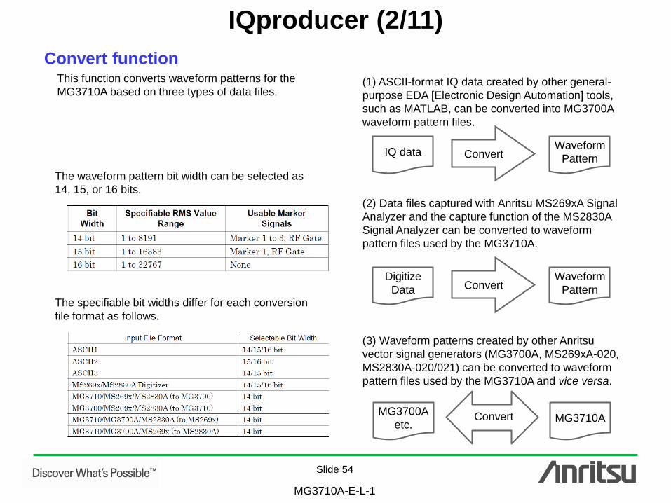
Convert function
(1) ASCII-format IQ data created by other general-
purpose EDA [Electronic Design Automation] tools,
such as MATLAB, can be converted into MG3700A
waveform pattern files.
IQ data Waveform
Pattern Convert
(2) Data files captured with Anritsu MS269xA Signal
Analyzer and the capture function of the MS2830A
Signal Analyzer can be converted to waveform
pattern files used by the MG3710A.
Digitize
Data
Waveform
Pattern Convert
(3) Waveform patterns created by other Anritsu
vector signal generators (MG3700A, MS269xA-020,
MS2830A-020/021) can be converted to waveform
pattern files used by the MG3710A and vice versa.
MG3700A
etc. MG3710A Convert
This function converts waveform patterns for the
MG3710A based on three types of data files.
The waveform pattern bit width can be selected as
14, 15, or 16 bits.
The specifiable bit widths differ for each conversion
file format as follows.

Slide 55
MG3710A-E-L-1
IQproducer (3/11)
Convert Function
Input file selection
Package name
File format
(See previous slide.)
Sampling rate
Range: 20 kHz to 160 MHz Normalizing
Sets amplitude value for converting
waveform pattern to RMS (Root Mean
Square), which is a standard waveform
pattern used for MG3710A.
Comment
Convert Setting Screen
Slide 56
MG3710A-E-L-1
IQproducer (4/11)
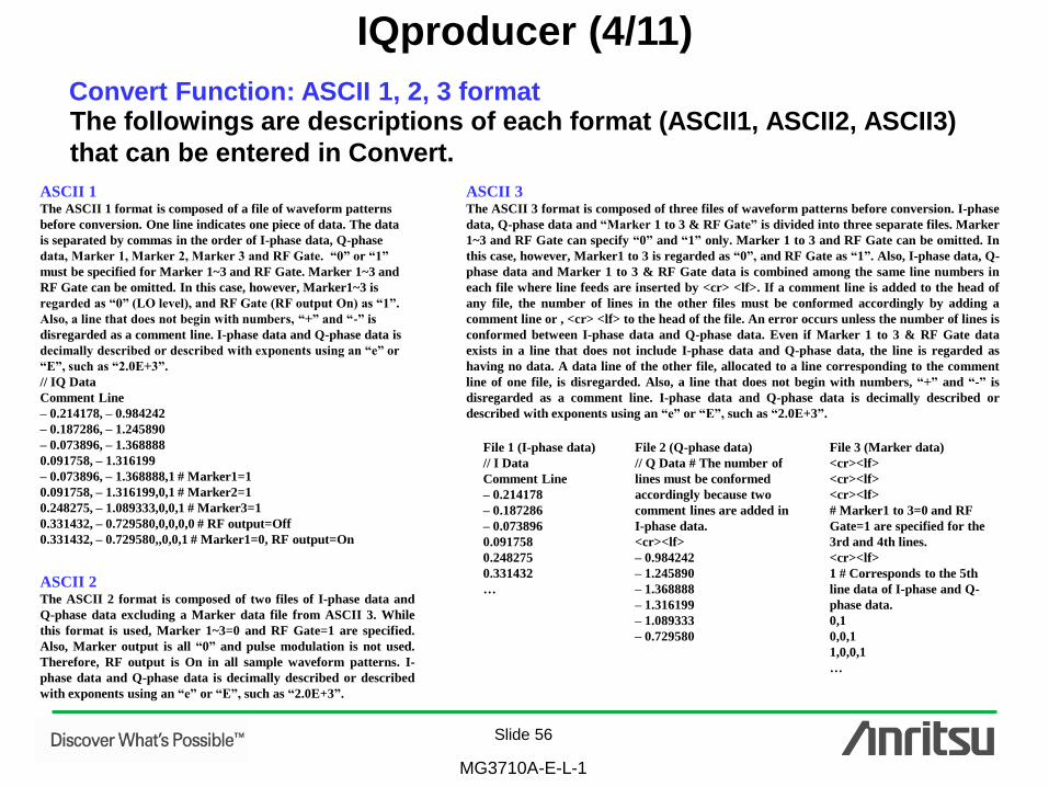
Convert Function: ASCII 1, 2, 3 format
ASCII 1 The ASCII 1 format is composed of a file of waveform patterns
before conversion. One line indicates one piece of data. The data
is separated by commas in the order of I-phase data, Q-phase
data, Marker 1, Marker 2, Marker 3 and RF Gate. “0” or “1”
must be specified for Marker 1~3 and RF Gate. Marker 1~3 and
RF Gate can be omitted. In this case, however, Marker1~3 is
regarded as “0” (LO level), and RF Gate (RF output On) as “1”.
Also, a line that does not begin with numbers, “+” and “-” is
disregarded as a comment line. I-phase data and Q-phase data is
decimally described or described with exponents using an “e” or
“E”, such as “2.0E+3”.
// IQ Data
Comment Line
– 0.214178, – 0.984242
– 0.187286, – 1.245890
– 0.073896, – 1.368888
0.091758, – 1.316199
– 0.073896, – 1.368888,1 # Marker1=1
0.091758, – 1.316199,0,1 # Marker2=1
0.248275, – 1.089333,0,0,1 # Marker3=1
0.331432, – 0.729580,0,0,0,0 # RF output=Off
0.331432, – 0.729580,,0,0,1 # Marker1=0, RF output=On
ASCII 2 The ASCII 2 format is composed of two files of I-phase data and
Q-phase data excluding a Marker data file from ASCII 3. While
this format is used, Marker 1~3=0 and RF Gate=1 are specified.
Also, Marker output is all “0” and pulse modulation is not used.
Therefore, RF output is On in all sample waveform patterns. I-
phase data and Q-phase data is decimally described or described
with exponents using an “e” or “E”, such as “2.0E+3”.
ASCII 3 The ASCII 3 format is composed of three files of waveform patterns before conversion. I-phase
data, Q-phase data and “Marker 1 to 3 & RF Gate” is divided into three separate files. Marker
1~3 and RF Gate can specify “0” and “1” only. Marker 1 to 3 and RF Gate can be omitted. In
this case, however, Marker1 to 3 is regarded as “0”, and RF Gate as “1”. Also, I-phase data, Q-
phase data and Marker 1 to 3 & RF Gate data is combined among the same line numbers in
each file where line feeds are inserted by <cr> <lf>. If a comment line is added to the head of
any file, the number of lines in the other files must be conformed accordingly by adding a
comment line or , <cr> <lf> to the head of the file. An error occurs unless the number of lines is
conformed between I-phase data and Q-phase data. Even if Marker 1 to 3 & RF Gate data
exists in a line that does not include I-phase data and Q-phase data, the line is regarded as
having no data. A data line of the other file, allocated to a line corresponding to the comment
line of one file, is disregarded. Also, a line that does not begin with numbers, “+” and “-” is
disregarded as a comment line. I-phase data and Q-phase data is decimally described or
described with exponents using an “e” or “E”, such as “2.0E+3”.
File 1 (I-phase data)
// I Data
Comment Line
– 0.214178
– 0.187286
– 0.073896
0.091758
0.248275
0.331432
…
File 2 (Q-phase data)
// Q Data # The number of
lines must be conformed
accordingly because two
comment lines are added in
I-phase data.
<cr><lf>
– 0.984242
– 1.245890
– 1.368888
– 1.316199
– 1.089333
– 0.729580
File 3 (Marker data)
<cr><lf>
<cr><lf>
<cr><lf>
# Marker1 to 3=0 and RF
Gate=1 are specified for the
3rd and 4th lines.
<cr><lf>
1 # Corresponds to the 5th
line data of I-phase and Q-
phase data.
0,1
0,0,1
1,0,0,1
…
The followings are descriptions of each format (ASCII1, ASCII2, ASCII3)
that can be entered in Convert.

Slide 57
MG3710A-E-L-1
IQproducer (5/11)
Clipping function This function performs clipping for a waveform pattern generated by each signal generation application. Filter,
bandwidth, and number of repetitions are set to generate a clipped waveform pattern.
Clipping Setting Screen
Input File
Selects waveform pattern for clipping
Repetition
Roll Off/BT (Enabled for Nyquist, Root Nyquist, Gaussian)
Setting Range: 0.10 to 1.00
Resolution: 0.01
Repeat count for clipping
and filtering
Setting Range: 1 to 20
Resolution: 1
Bandwidth Setting Range: Sampling Rate/1000 or 0.001
~ Sampling Rate
Threshold Level
Level for clipping
Setting Range: 0 to 20 dB
Resolution: 0.1 dB
Clipping is used when restricting the input signal peak, such as
at amplifier evaluation.
In addition, it can also be used to filter unwanted signals at the
adjacent channel for Rx test interference patterns.
Filter Type
Ideal,
None,
Nyquist,
Root Nyquist,
Gaussian

Slide 58
MG3710A-E-L-1
IQproducer (6/11)
CCDF Function The Complementary Cumulative Distribution Function (CCDF) of a waveform pattern generated by a signal
generation application can be displayed.
In a CCDF graph, the signal peak/average power is displayed on the x-axis, and the cumulative probability that the
signal peak/average power is equal to or less than the value on the x-axis is displayed on the y-axis. As a result, the
distribution of peak powers of various modulation signals are displayed on the screen. This is convenient for
estimating the output waveform distortion characteristics when a generated signal is input from the MG3710A to a
power amplifier or other devices.
CCDF Screen
Gaussian Trace
Waveform Patterns Select up to 8
waveform
patterns.
Slide 59
MG3710A-E-L-1
IQproducer (7/11)
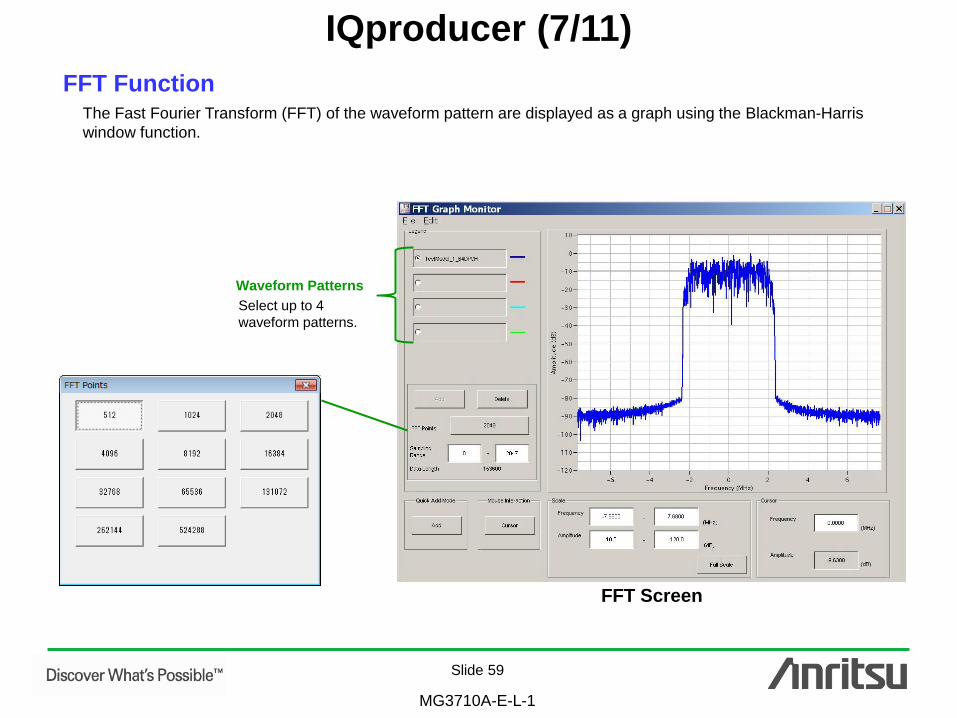
FFT Function The Fast Fourier Transform (FFT) of the waveform pattern are displayed as a graph using the Blackman-Harris
window function.
FFT Screen
Waveform Patterns
Select up to 4
waveform patterns.
Slide 60
MG3710A-E-L-1
IQproducer (8/11)
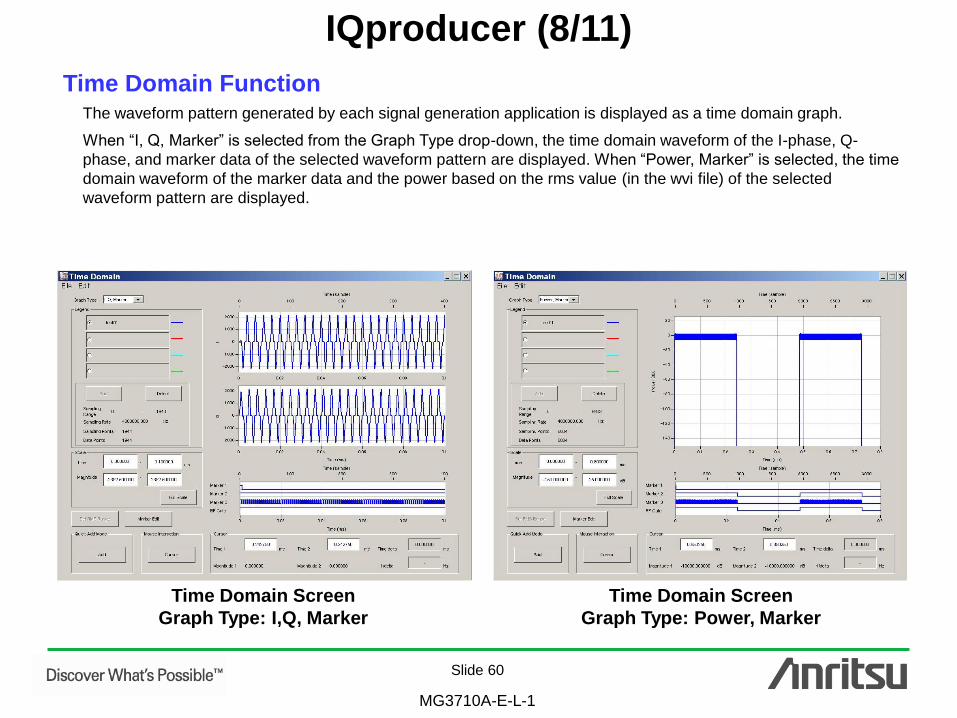
Time Domain Function The waveform pattern generated by each signal generation application is displayed as a time domain graph.
When “I, Q, Marker” is selected from the Graph Type drop-down, the time domain waveform of the I-phase, Q-
phase, and marker data of the selected waveform pattern are displayed. When “Power, Marker” is selected, the time
domain waveform of the marker data and the power based on the rms value (in the wvi file) of the selected
waveform pattern are displayed.
Time Domain Screen
Graph Type: I,Q, Marker
Time Domain Screen
Graph Type: Power, Marker

Slide 61
MG3710A-E-L-1
IQproducer (9/11)
Time Domain: Marker Edit A new waveform pattern can be created by reading an existing waveform pattern and editing the marker data and
name using this function.
Time Domain screen
Marker Edit Screen

Slide 62
MG3710A-E-L-1
IQproducer (10/11)
Transfer & Setting Function When changing the MG3710A network setting to DHCP Off and connecting the MG3710A and PC using a LAN
crossover cable, restart the MG3710A after changing the network setting before connecting the LAN cable.
LAN Crossover Cable
PC
Input MG3710A IP address.
MG3710A

Slide 63
MG3710A-E-L-1
IQproducer (11/11)
Transfer & Setting: Operation
PC side MG3710A side
Connects/Dis
connects
Deletes file
Transfers file Installs license key
Loads and clears waveform
pattern in waveform memory
Starts
waveform
pattern output
Slide 64
MG3710A-E-L-1
Note

• United StatesAnritsu Company1155 East Collins Blvd., Suite 100, Richardson, TX 75081, U.S.A.Toll Free: 1-800-267-4878Phone: +1-972-644-1777Fax: +1-972-671-1877
• CanadaAnritsu Electronics Ltd.700 Silver Seven Road, Suite 120, Kanata, Ontario K2V 1C3, CanadaPhone: +1-613-591-2003 Fax: +1-613-591-1006
• Brazil Anritsu Eletrônica Ltda.Praça Amadeu Amaral, 27 - 1 Andar01327-010 - Bela Vista - São Paulo - SP - BrazilPhone: +55-11-3283-2511Fax: +55-11-3288-6940
• MexicoAnritsu Company, S.A. de C.V.Av. Ejército Nacional No. 579 Piso 9, Col. Granada11520 México, D.F., MéxicoPhone: +52-55-1101-2370Fax: +52-55-5254-3147
• United KingdomAnritsu EMEA Ltd.200 Capability Green, Luton, Bedfordshire, LU1 3LU, U.K.Phone: +44-1582-433200 Fax: +44-1582-731303
• FranceAnritsu S.A.12 avenue du Québec, Bâtiment Iris 1- Silic 612,91140 VILLEBON SUR YVETTE, FrancePhone: +33-1-60-92-15-50Fax: +33-1-64-46-10-65
• GermanyAnritsu GmbHNemetschek Haus, Konrad-Zuse-Platz 1 81829 München, Germany Phone: +49-89-442308-0 Fax: +49-89-442308-55
• ItalyAnritsu S.r.l.Via Elio Vittorini 129, 00144 Roma, ItalyPhone: +39-6-509-9711 Fax: +39-6-502-2425
• SwedenAnritsu ABBorgarfjordsgatan 13A, 164 40 KISTA, SwedenPhone: +46-8-534-707-00 Fax: +46-8-534-707-30
• FinlandAnritsu ABTeknobulevardi 3-5, FI-01530 VANTAA, FinlandPhone: +358-20-741-8100Fax: +358-20-741-8111
• DenmarkAnritsu A/S (Service Assurance)Anritsu AB (Test & Measurement)Kay Fiskers Plads 9, 2300 Copenhagen S, DenmarkPhone: +45-7211-2200Fax: +45-7211-2210
• RussiaAnritsu EMEA Ltd. Representation Office in RussiaTverskaya str. 16/2, bld. 1, 7th floor.Russia, 125009, MoscowPhone: +7-495-363-1694Fax: +7-495-935-8962
• United Arab EmiratesAnritsu EMEA Ltd.Dubai Liaison OfficeP O Box 500413 - Dubai Internet CityAl Thuraya Building, Tower 1, Suit 701, 7th FloorDubai, United Arab EmiratesPhone: +971-4-3670352Fax: +971-4-3688460
• IndiaAnritsu India Private Limited2nd & 3rd Floor, #837/1, Binnamangla 1st Stage, Indiranagar, 100ft Road, Bangalore - 560038, IndiaPhone: +91-80-4058-1300Fax: +91-80-4058-1301
• SingaporeAnritsu Pte. Ltd.60 Alexandra Terrace, #02-08, The Comtech (Lobby A)Singapore 118502Phone: +65-6282-2400Fax: +65-6282-2533
• P.R. China (Shanghai)Anritsu (China) Co., Ltd.Room 1715, Tower A CITY CENTER of Shanghai, No.100 Zunyi Road, Chang Ning District, Shanghai 200051, P.R. ChinaPhone: +86-21-6237-0898Fax: +86-21-6237-0899
• P.R. China (Hong Kong)Anritsu Company Ltd.Unit 1006-7, 10/F., Greenfield Tower, Concordia Plaza,No. 1 Science Museum Road, Tsim Sha Tsui East, Kowloon, Hong Kong, P.R. ChinaPhone: +852-2301-4980Fax: +852-2301-3545
• JapanAnritsu Corporation8-5, Tamura-cho, Atsugi-shi, Kanagawa, 243-0016 JapanPhone: +81-46-296-1221Fax: +81-46-296-1238
• KoreaAnritsu Corporation, Ltd.502, 5FL H-Square N B/D, 681Sampyeong-dong, Bundang-gu, Seongnam-si, Gyeonggi-do, 463-400 KoreaPhone: +82-31-696-7750Fax: +82-31-696-7751
• AustraliaAnritsu Pty. Ltd.Unit 21/270 Ferntree Gully Road, Notting Hill, Victoria 3168, AustraliaPhone: +61-3-9558-8177Fax: +61-3-9558-8255
• TaiwanAnritsu Company Inc.7F, No. 316, Sec. 1, NeiHu Rd., Taipei 114, TaiwanPhone: +886-2-8751-1816Fax: +886-2-8751-1817
Specifications are subject to change without notice.
1209
Printed on Recycled Paper
Please Contact:
No. MG3710A-E-L-1-(3.00) Printed in Japan 2013-3 MG