In Situ Friction Measurements in Chemical Mechanical Planarization

University of South FloridaScholar Commons
Graduate Theses and Dissertations Graduate School
2005
Processing, reliability and integration issues inchemical mechanical planarizationParshuram B. ZantyeUniversity of South Florida
Follow this and additional works at: http://scholarcommons.usf.edu/etd
Part of the American Studies Commons
This Dissertation is brought to you for free and open access by the Graduate School at Scholar Commons. It has been accepted for inclusion inGraduate Theses and Dissertations by an authorized administrator of Scholar Commons. For more information, please [email protected].
Scholar Commons CitationZantye, Parshuram B., "Processing, reliability and integration issues in chemical mechanical planarization" (2005). Graduate Theses andDissertations.http://scholarcommons.usf.edu/etd/928

Processing, Reliability And Integration Issues In Chemical Mechanical Planarization
By
Parshuram B. Zantye
A dissertation submitted in partial fulfillment of the requirements for the degree of
Doctor of Philosophy in Mechanical Engineering Department of Mechanical Engineering
College of Engineering University of South Florida
Major Professor: Ashok Kumar, Ph.D. Rajiv Dubey, Ph.D.
Muhammad Rahman, Ph.D. Tapas Das, Ph.D.
Julie Harmon, Ph.D. John Bumgarner, Ph.D.
Yaw Obeng, Ph.D.
Date of Approval: July 15 2005
Keywords: chemical mechanical polishing (cmp), tribology, polishing pad, slurry, damascene, metrology, end point, delamination, ultrasound, reliability
© Copyright 2005, Parshuram B. Zantye

DEDICATION
My entire work in the field of Chemical Mechanical Planarization including this
dissertation is dedicated to my Parents, Mrs. Vrinda B. Zantye and Mr. Balkrishna P.
Zantye.

ACKNOWLEDGMENTS
I would like to generously thank my advisor Prof. Ashok Kumar for giving me
an opportunity to pursue research under his able guidance and with his support
throughout during my Masters’ as well as Doctoral studies at University of South Florida.
I would like to thank the Chairman of Department of Mechanical Engineering, Prof.
Rajiv Dubey for his constant encouragement and assistance throughout my tenure as a
graduate student, and also for serving my dissertation committee. A special thanks goes
to Dr. Yaw Obeng (Texas Instruments, Dallas, TX) for his invaluable help in terms of
sharing technical know how all along the course of my research during his tenure earlier
at psiloQuest Inc, Orlando, FL and later at Texas Instruments, Inc. I wish to thank the
Chair of my dissertation committee, Prof. Sunil Saigal for serving on my committee and
giving me invaluable suggestions for this past year. I would like to highly acknowledge
the help of Dr. Michael Kovac, Director, Nanomaterials and Nanomanufacturing
Research Center (NNRC) and all the team of engineers, technicians and support staff
working under his able leadership at the NNRC. Special thanks also go to all my
committee members: Dr. Mohammed Rahman, Dr. Tapas Das, Dr. Julie Harmon, and Dr.
John Bumgarner. Also, I wish to thank Dr. Sergei Ostapenko, who for logistic reasons
could not serve on my committee but was actively involved with my research. The
financial support for this research came from NSF CAREER Grant #9983535 (Ashok
Kumar) and NSF GOALI Grant #DMII 0218141. Part of this research was also supported
by USF-Agere High-Tech Corridor Grant #2112-142LO, International Sematech Grant #
2112-139 and psiloQuest, Inc. Florida High Tech Corridor Grant. I would also like to

thank Dr. Ashok Das from Applied Materials, Dr. Jeffery Lee from Intel Corporation,
Dr. M. Sanganeria from Novellus Systems, and Dr. Jiro Yota from Skyworks Inc., for
providing valuable inputs, materials and supplies. Finally, my parents, family, friends,
former Post Doctoral fellows (Dr. Arun K. Sikder and Dr. Arun Kumar), and colleagues,
especially S. Mudhivarthi, also deserve a very special thank you note at this time for
constantly supporting me throughout the thick and thin of my life.

i
TABLE OF CONTENTS LIST OF TABLES vii LIST OF FIGURES viii ABSTRACT xvii CHAPTER 1: INTRODUCTION 1 1.1 Generalized Semiconductor Fabrication Modules 1 1.2 Increase in Device Density 2 1.3 Scaling and Time Delay 3 1.4 Need for Planarization 9 1.5 Shallow Trench Isolation 10
1.6 Damascene Process 12 1.7 Different Planarization Techniques 13
1.7.1 Doped Glass Reflow 14
1.7.2 Spin Etch Planarization (SEP) 16
1.7.3 Spin on Deposition (SOD) 17
1.7.4 Reactive Ion Etch and Etch Back (RIE+EB) 19
1.7.5 Chemical Mechanical Planarization (CMP) 20
1.8 General Chemical Mechanical Planarization Applications 21 1.9 Overview 26

ii
CHAPTER 2: BACKGROUND OF CMP 27
2.1 Evolution of CMP 27
2.1.1 History of CMP 27
2.1.2 Road Map of CMP Process 28
2.2 CMP: A Multi-stage Process 31
2.2.1 Slurry Mixing 33
2.2.2 Slurry Distribution 34
2.2.3 Working of the CMP Process 35
2.2.4 CMP Polisher Consideration 36
2.2.5 First Generation CMP Polisher 37
2.2.6 Second Generation CMP Polisher 38
2.2.6.1 Multi-wafer Per Platen Polisher 38
2.2.6.2 Sequential Rotational Systems 39
2.2.7 Third Generation Polishers 40
2.2.7.1 Sequential Linear Polishers 40
2.2.7.2 Orbital Polishers 41
2.2.7.3 Rotary Inverted 42
2.2.7.4 Pad Feed Polishers 43
2.3 Physics of CMP Process 44
2.4 Parameters Governing CMP Process 46
2.5 Research Objectives 48

iii
CHAPTER 3: METROLOGY OF CMP 49
3.1 Need for Effective CMP Metrology 49
3.2 CMP Tester 50
3.3 Coefficient of Friction (COF) and Material Removal Rate (MRR) 52
3.4 Importance of Slurry Flow 55
3.5 CMP End Point Detection (EPD) 58
3.6 In-situ Process Monitoring 63
3.7 Delamination during CMP 72
3.8 Other CMP Defects 76
CHAPTER 4: PROPERTIES OF INTERCONNECT MATERIALS 77
4.1 Need for Evaluation of Material Properties 77
4.2 Effect of Annealing on Copper 78
4.3 Significance of Interfacial Reliability in Damascene Structure 81
4.4 Effect of Annealing on Cu-TaN Interface 82
4.5 Techniques of Interfacial Evaluation of Thin Films 83
4.5.1 Four Point Bend Technique 84
4.5.2 Nanoscratch Testing 86
4.5.2.1 Failure Domain Analysis of Nanoscratch Tests 89
4.5.2.1.1 SEM/Auger Spectroscopy Analysis 89
4.5.2.1.2 FIB Cross section and SEM Analysis 92
4.6 Quantitative Evaluation of Thin Film Adhesion Energy 93

iv
4.7 Qualitative Evaluation of Thin Film Adhesion Energy 95
4.8 Low Dielectric Constant Materials (low k materials) 96
4.8.1 CVD Based Low k Materials 98
4.8.2 Spin On Low k Materials 99
4.8.3 Potentially Feasible Low k Materials 100
4.9 Mechanical Characterization of Low k Materials 103
4.10 CMP of Low k Materials 107
4.10.1 Doped and Undoped Ceramic Material Removal 108
4.10.2 Polymeric Material Removal 109
4.10.3 CMP Process Conditions 110
4.10.4 Tribological Properties of Low k Materials 112
4.10.5 Variation of Material Removal Rate for Low k Materials 116
4.10.6 Surface Characterization of Low k Materials 118
4.10.7 Findings of Low k Materials Evaluation 120
CHAPTER 5: INVESTIGATION OF NON UNIFORMITIES IN POLISHING PAD 123
5.1 Significance of Polishing Pad 123
5.2 Method of Mapping and Isolation of Pad Non-Uniformities 124
5.3 Ultrasound Testing System 126
5.4 Evaluation of Mechanical and Tribological Properties of Polishing Pad 128
5.5 SEM Evaluation of Polishing Pad 130
5.6 Isolation of Polishing Pad Coupons 131
5.7 Isolation of 6 Inch Polishing Pad Coupons 133

v
5.8 Pad Dynamic Mechanical Analysis 134
5.9 Frictional Characteristics of Polishing Pad Regions 137
5.10 Summary of Investigations of Polishing Pad Non uniformities 143
CHAPTER 6: INVESTIGATION AND OPTIMIZATION OF APPLICATION
SPECIFIC CMP PADS 144
6.1 Application Specific Pad (ASP) for CMP 144
6.2 Scheme for Optimization of ASP Properties 146
6.3 Experimental Techniques for ASP Property Evaluation 147
6.4 Evaluation of ASP Surface Micromechanical Properties 149
6.5 Evaluation of ASP Surface Micromechanical Properties 153
6.6 Evaluation of Static Tribological Properties of ASP 157
6.7 CMP (Dynamic Tribological Property) Evaluation of ASP 158
6.8 Optimization of ASP Total Thickness 163
6.9 Summary of ASP Optimization and Characterization 165
CHAPTER 7: INDENTIFICATION AND MODIFICATION OF CMP SLURRY 167
7.1 Background of CMP Slurry 167
7.2 Effect of CMP Slurry in Global Planarization 167
7.3 Effect of CMP Slurry on Removal Rate 170
7.3.1 Effect of Slurry Chemistry on Removal Rate 171
7.3.2 Effect of Slurry Particle Size Hardness and Concentration 172
7.4 Effect of Temperature on Slurry Performance 174

vi
7.5 Novel Nanoparticle Based Slurry 177
7.5.1 Composition of Novel Nanoparticle Based Cu Slurry 178
7.5.2 Mechanism of Polishing of Novel Cu Slurry 179
7.5.3 Polishing Performance of Novel Nanoparticle Cu Slurry 182
7.6 Summary of Investigation and Modification of CMP Slurry 185
CHAPTER 8: SUMMARY 187
8.1 Summary of Research 187
8.2 Major Findings and Contributions 189
8.3 Future Trends in CMP and Potential Areas for Investigation 191
REFERENCES 193 ABOUT THE AUTHOR End Page

vii
LIST OF TABLES
Table 1.1 Interconnection Delay (RC) in Silicon VLSI Chip 6 Table 1.2 Advantages of Chemical Mechanical Planarization 23 Table 1.3 Disadvantages of Chemical Mechanical Planarization 24 Table 1.4 Applications of Chemical Mechanical Planarization 25
Table 2.1 Interconnect International Technology Roadmap for Semiconductors 30
Table 3.1 Effect of Slurry Flow rate on COF and AE 56
Table 3.2 STI-CMP Experimental Details 66
Table 4.1 Details of the Samples Undergoing Two Stage Annealing 79
Table 4.2 Details of the Samples Subjected to Interfacial Studies 83
Table 4.3 Relative Concentration of the Elements (at.%) on Scratch Surface 91
Table 4.4 Details of the Different Low k Materials Evaluated 105
Table 4.5 Results of Nanoindentation of the ILD materials 106
Table 4.6 ILD CMP Experimental Details 111
Table 4.7 Surface Roughness (Rrms) of the ILD Samples Before and After CMP 120
Table 5.1 Details of the CMP Experiments Performed on the Polishing Pad
evaluated by UST 129
Table 6.1 Experimental Details of CMP Process Used for ASP Evaluation 149
Table6.2 Multivariate Correlations between Various Independent Results and
PECVD Coating Time 162

viii
LIST OF FIGURES Figure 1.1 Scanning Electron Micrographs of Cross-section of the Structures
Fabricated by BEOL Technology: (a) BEOL structure of 0.5 µm
CMOS Logic Device and (b) Stacked Contacts and Vias 2
Figure 1.2 Trends Over the Years in Logic and Memory Devices 3 Figure 1.3 Chronology of Key Interconnect Technology Introduction Through
the Years. LM Denotes Levels of Metallization 4
Figure 1.4 Variation of RC Time Delay with Minimum Feature Size 7 Figure 1.5 Predicted Future Trends in IC Interconnect Technology, (Courtesy:
Jeffery Lee, Intel Corporation) 8
Figure 1.6 Chart Showing Decrease in Intermediate Interconnect Wiring Pitch for
Future Generation IC, (Courtesy: Jeffery Lee, Intel Corporation) 8
Figure 1.7 Schematic of a) Non-planarized and b) Planarized MLM structure 10 Figure 1.8 Schematic of a Processes Sequence of Direct STI CMP without
Reverse Moat 11
Figure 1.9 Comparison between Subtractive Etch (Conventional Approach) and
the Damascene Approach for Metallization 13
Figure 1.10 Schematic Showing Degrees of Surface Global and Local Planarity 14
Figure 1.11 Schematic Showing BPSG Void Formation after Reflow 15

ix
Figure 1.12 Schematic of SEP Chamber Showing a Cut-away View of the Process
Pot, Four Chambers and Chuck. The Chemical Dispense Arm, Drain
Lines and Exhaust Ports also are Indicated 17
Figure 1.13 Schematic showing Spin on Deposition with Partial planarization 18 Figure 1.14 Schematic Showing Smoothening and Partial Planarization using
Reactive Ion Etching with Etch Back 20
Figure 1.15 Scanning Electron Micrograph Showing Cross-section of Structure
Planarized by SOD RIE EB 21
Fig. 2.1 Flow Chart of the Isolated Industrial CMP Process 31
Fig. 2.2 Schematic of the Slurry Mixing at a Centralized Location 33
Fig. 2.3 Schematic of CMP Slurry Distribution System 34
Fig. 2.4 Schematic of Wafer Planarization by CMP Process 35
Fig. 2.5 Photograph of Speefam (Novellus) Multi Wafer per Platen Polisher 38
Fig. 2.6 Applied Materials Inc., Sequential Rotational CMP Polisher (Courtesy:
Ashok Das, Applied Materials, Inc., Santa Clara, CA) 39
Fig. 2.7 Photograph of Sequential Linear Polishing System 41
Fig. 2.8 Schematic of Rotary CMP Polisher 42
Fig. 2.9 a) Set up of Multi Wafer Rotary Inverted CMP Polisher and b)
Polishing Action and End Point detection 43
Fig. 2.10 Schematic of a Web-type Polisher 44
Fig. 2.11 Schematic of the Force Field on the Wafer and the Pad during CMP 45
Fig. 2.12 Non-uniformity in Removal Rate with in a Wafer 46

x
Fig. 2.13 Parameters Governing the CMP Dynamics 47
Fig. 2.14 Schematic Showing Objectives of the Current Research 48
Fig. 3.1 Photograph of the CETR CP-4 CMP Tester 51
Fig. 3.2 a) Variation of COF with RPM (platen velocity) for Different Values
of Down Pressure (PSI), b) Variation of COF with PSI
(Down Pressure) with Different Values of Platen Velocity (RPM) 53
Fig. 3.3 a) Variation of Average Removal Rate with RPM at Different Down
Pressure (PSI) for the Evaluated Set of Samples, b) Variation of
Average Removal Rate with PSI (Down Pressure) at Different Platen
Velocity (RPM) for the Evaluated Set of Samples 54
Fig. 3.4 Average Material Removal Rates Plotted with RPM × PSI. Linear
Relation Indicates that Polishing Follows Preston's Equation 55
Fig. 3.5 Schematic of the Positions of Slurry Feeding on the Pad during
Polishing for Feeding Position Optimization; Distance 0–1.4 = 15 mm,
0–2.5 = 30 mm, 0–3.6 = 45 mm, 0–7.9 = 45 mm and 0–8 = 25 mm 56
Fig. 3.6 Average Removal Rate with the Slurry Feeding Position on the Lower
Platen Position 57
Fig. 3.7 a) Variation of COF at 2 PSI Down Force and Variable RPM in Slurry
Cu1; b) Variation of COF at 2 PSI Down Force and Variable RPM in
Slurry Cu2; c) Variation of COF at 2 PSI Down Force and Variable
RPM in Slurry Ta; and d) Variation of COF at 2 PSI Down Force and
Variable RPM in Slurry Cu–Ta 59

xi
Fig. 3.8 a) Variation of AE and COF for Different Materials Polished in a
Commercial Cu Slurry, b) Variation of COF for 3 Materials Polished
in Three Different Slurries 60
Fig.3.9 Cu and TaN Polishing Results (Head 40 RPM, Table 40 RPM, and
Pressure 7 PSI) 61
Fig. 3.10 Schematic Illustration of Dishing and Erosion 63
Fig. 3.11 SEM of FIB Cross Section of STI Structure 64
Fig. 3.12 3D AFM Image of the Evaluated STI Structure with Step Height
Measurement 65
Fig. 3.13 In-situ Variation of COF during CMP Split in to Different Stages 68
Fig. 3.14 Ex-situ 3D AFM Image of the Evaluated STI Structure with Reduced
Step Height before Termination of Stage A 68
Fig. 3.15 Ex-situ 3D AFM image of the Evaluated STI Structure after Process
End Point just after Beginning of Stage B 69
Fig. 3.16 In-situ data for Repeatability of 2 Trial Runs Shown to Demonstrate
Repeatability 71
Fig. 3.17 a) Picture of Sample Coupons ACL, BCL, and TC after Polishing, b)
Variation of AE signal of Three Different Samples 73
Fig. 3.18 SEM Micrographs Showing of Delamination of Different ACL, BCL
Samples and No Delamination for TC Sample 74
Fig. 3.19 a) Variation of AE Signal during Polishing in the Time Interval of
230 – 250 s for Three Different Samples. Peaks are Seen for Sample
ACL006, b) Sample ACL006 and (c) Sample A006r 75

xii
Fig. 4.1 Challenges Surrounding Implementation of Novel Low k Materials
Cu in a Damascene Structure (Courtesy: Jeffery Lee,
Intel Corporation) 81
Fig. 4.2 Schematic of Four Point Bend Test (University of California,
Santa Barabara) Set Up 84
Fig. 4.3 Variation of Load (lbf) Vs Displacement (Microns) during a Four
Point Bend Test 85
Fig. 4.4 Schematic of the Nanoscratch Testing Setup 88
Fig. 4.5 Raw Data Showing the Variation of a) Acoustic Emission (AE),
b) Frictional Force (Ff) with Time during a Scratch Test.
(Sample 1 at Linearly Increasing Downward Force of 2 gm/sec
Linear Velocity of 0.2 mm/sec) 88
Fig. 4.6 Surface SEM of the Nanoscratch at Region a) at the Initial
Stages of Microscratch, and b) Upon Completion of Delamination 90
Fig. 4.7 FIB Cross-section and SEM Micrograph of the Thin Film Obtained a
Region of Onset of Delamination 92
Fig. 4.8 Variation of Interfacial Adhesion Energy for the Different
Samples Evaluated by Four Point Bend Technique 93
Fig. 4.9 Elemental Dispersion Spectroscopy Analysis of the Failed Interface
after Four Point Bend Analysis 95
Fig. 4.10 Variation of Critical Load for Different Evaluated Samples
obtained from the Nanoscratch Test 96
Fig. 4.11 Simplified Classification of Low k Dielectrics 102

xiii
Fig. 4.12 Typical Curve Showing the Loading and Unloading as a Function
of Indenter Penetration Depth 105
Fig. 4.13 Variation of the Normalized Hardness with Dielectric Constant
of the Candidate ILD Materials 107
Fig. 4.14 Material Removal Schematic during Ceramic ILD CMP 108
Fig. 4.15 Schematic showing the Action of ILD Slurry on the Polymer Surface
during CMP 110
Fig. 4.16 Variation of COF with Down Pressure (PSI) and Linear Velocity (m/s)
for a) SiO2U, b) SiOF, c)Polyimide, and d) BCB 113
Fig. 4.17 Variation of MRR with Pressure (P) and Platen RPM
(Linear Velocity V) for a) SiO2 (U), b) SiOF, c) Polyimide, d) BCB 117
Fig. 4.18 Surface Morphology of the Candidate ILD Samples Before and After
CMP for: a) SiO2 (U), b) SiOF, c) Polyimide and d) BCB 121
Fig. 5.1 Schematic of the Construction of the Ultrasound Testing Equipment 125
Fig. 5.2 Cross-section Scanning Electron Micrograph of the Evaluated
Commercial Polyurethane Polishing pad with a Sub-pad 130
Fig. 5.3 Ultrasonic Transmission Maps of the Quarter IC1000/SubaIV pad a)
Before and b) After punching of the 1” coupons. Three coupons were
punched at the High-Intensity (white) Area and Four Coupons at Low-
Intensity (Black) Area. The Effect of Pad Acoustic Homogenization
after Punching is Illustrated in Respective Histograms (b, d) 132
Fig. 5.4 a) Pad Mapped Before Punching 6-inch Coupons, b) Area of Pad
Remapped after Replacing the Punched HT Coupon, c) Area of Pad

xiv
Remapped after Replacing the Punched LT Coupon (All the Values
have been Normalized over the Entire Area). 135
Fig. 5.5 a) Variation of Storage Modulus Vs Temperature, b) Variation of
loss modulus Vs Temperature c) Variation of tan δ Vs Temperature
of Samples Tested from Low and High Intensity region of the Pad 136
Fig. 5.6 Ultrasound Transmission Scan of Pad with Sub-pad 138
Fig. 5.7 Ultrasound Transmission Scan of Pad without Sub-pad 138
Fig. 5.8 Variation of COF for a) Pad 1 and b) Pad 2 during the CMP Process
for the Various Values of PSI and RPM 142
Fig. 6.1 Cross-sectional SEM micrograph of a) PsiloQuest’s ASP and b)
Commercial Polyurethane Polishing pad with a sub pad 150
Fig.6.2 Loading and Unloading Behavior Exhibited by the PsiloQuest’s ASP
coated for 10 minutes (Pad 1). Note the non-linearity at the Specific
Sites of the Loading and Unloading Curve Represent Plastic
Deformation under Indentation. 151
Fig.6.3 The Variation of Depth of First Non-linearity of in the Loading Curve
(Xa) as a Function of PECVD-TEOS Coating Time for Different Pads
Evaluated 152
Fig.6.4 Variation of Elastic Modulus and Hardness with TEOS Coating Time
Evaluated by Nanoindentation for Different Evaluated Polishing Pads 153
Fig. 6.5 X Ray Photoelectron Spectroscopy (XPS) Data for Polishing Pads
with Different TEOS Surface Coating Time 155

xv
Fig.6.6 Variation in Surface Silanol / Silicates in PECVD-TEOS Coating as a
Function of TEOS Deposition Time 156
Fig. 6.7 Variation of Static Wear Rate and Static Coefficient of Friction for
Pads with Different PECVD TEOS Surface Coating Time 157
Fig. 6.8 Variation of the Average Value of COF (taken for First 60 Seconds) for
the Different Candidate Pads during the Polishing Runs at 2 PSI Down
Force and 150 RPM Platen Rotation 158
Fig.6.9 Variation of the Average Value of MRR for the Different Candidate
Pads during the Polishing Runs at 2 PSI Down Force and 150 RPM
Platen Rotation 159
Fig.6.10 Variation of COF for Different Total ASP Thickness for an Optimized
Surface Coating Time of 40 Minutes 164
Fig. 6.11 Variation of MRR for Different Total ASP Thickness for an Optimized
Surface Coating Time of 40 Minutes 165
Fig. 7.1 Prime Criteria for Slurry Design 168
Fig. 7.2 Schematic of Microscale and Nanoscale Phenomena during CMP 170
Fig. 7.3 Variation of Rate of Surface Layer Formation in Cu with Different
Slurry Chemistry 171
Fig. 7.4 Transient Electrochemical Chronoamperometry Measurements of W 171
Fig. 7.5 Variation of Removal Rate with Particle Size and Concentration 173
Fig. 7.6 Removal Rate of Silica with Different Particle Size and Concentration 174
Fig. 7.7 Variation of COF and MRR with Increase in Slurry Temperature 176

xvi
Fig. 7.8 Variation of ln of MRR in m/s with Inverse of Temperature (1/T)
Showing an Arrhenius Relationship 176
Fig. 7.9 Schematic Showing Mechanism of Polishing Action of Novel
Nanoparticle CMP slurry 181
Fig. 7.10 Variation of MRR for Different Trials Using Nanoparticle Slurry
without the Surface Catalyst 182
Fig. 7.11 Variation of MRR for Different CMP Trials for Nanoparticle Slurry
with Surface Catalyst 183
Fig. 7.12 Variation of COF for Different CMP Trials Using Novel Nanoparticle
Based CMP slurry 183
Fig. 7.13 Variation of COF with Time Measured In-situ for Polishing of EP Cu
Samples Under 3 PSI Down Pressure and 100 RPM Platen Rotation
Using a) Novel Nanoparticle Cu Slurry, and b) Commercial Cu Slurry 184

xvii
PROCESSING, RELIABILITY AND INTEGRATION ISSUES IN CHEMICAL
MECHANICAL PLANARIZATION
Parshuram B. Zantye
ABSTRACT
Global planarization is one of the major demands of the semiconductor
industry. Chemical mechanical polishing (CMP) is the planarization method of choice
use to achieve the required stringent tolerances essential for successful fabrication of next
generation Integrated Circuits (IC). The predominant reason for CMP defects is the shear
and normal stresses during polishing to which the material is subjected. Understanding
the process of CMP and factor that contribute to overall stress addition during polishing
requires an approach that encompasses all the four major categories of variables, namely:
a) machine parameters, b) material properties, c) polishing pad characteristics, and d)
polishing slurry performance. In this research, we studied the utilized in-situ technique
involving acoustic emission (AE) signal monitoring and coefficient of friction (COF)
monitoring using a CETRTM Bench Top CMP Tester to evaluate the impact of variation
in machine parameters on the CMP process. The mechanical and tribological properties
of different candidate materials have been evaluated bring potential challenges in their
integration to the fore. The study also involves destructive and non destructive testing of
polishing pads performed for characterization and optimization of polishing pad

xviii
architecture. Finally, the investigation concludes proposing novel nanoparticle CMP
slurry which has a predominant chemical component in its polishing mechanism. It was
found that the decrease in the mechanical shear and normal loading by: a) operating the
process in the low stress regime, b) using potential materials that are mechanically
stronger, c) using polishing pads with lesser variation in specific gravity and with a
surface that is has its mechanical properties fine tuned to those of the wafer, and d)
deploying polishing slurry with a significant chemical component mechanical removal,
are some of the approaches that can be employed to meet the future challenges of the
CMP process and reduce the defect associated with it.

1
CHAPTER ONE
INTRODUCTION
1.1 Generalized Semiconductor Fabrication Processes
The relentless competitor and customer driven demand for increased circuit
density, functionality and versatility has led to evolutionary and revolutionary advances
in the “front end” of the chip manufacturing line where the devices are fabricated, and the
“back end” where these devices are appropriately wired within the integrated circuit (IC)
[1]. Chip interconnections, or “interconnects,” serve as local and global wiring,
connecting circuit elements and distributing power [2]. To incorporate and accommodate
the improvements such as decreased feature size, increased device speed and more
intricate designs, research in the ‘back end of the line’ (BEOL) processes has become
equally important as the development of the ‘front end of line’ (FEOL) processes to
reduce gate oxide thickness and channel length. Fig. 1.1 (a and b) shows the multilevel
interconnect structure which is fabricated using the BEOL processes. The current viable
technologies and future trends in scaling bipolar and Complimentary Metal Oxide
Semiconductor (CMOS) devices fabrication and FEOL technologies have been discussed
at length by Taur et al. [3].

2
Fig.1.1 Scanning Electron Micrographs of Cross-section of the Structures Fabricated by
BEOL Technology: (a) BEOL Structure of 0.5 µm CMOS Logic Device and (b) Stacked
Contacts and Vias [1].
1.2 Increase in Device Density
Over the last 20 years, circuit density has increased by a factor of
approximately 104 (Fig. 1.2), while cost has constantly decreased [e.g., the historical 27%
per year decline in price per bit for dynamic random access memories (DRAMs)] [3].
The trend is expected to continue in the future even as 45 nm processes are set for
production in 2007 [4]. While recent path breaking innovations in the field of lithography
and patterning [5- 9] have brought about progressive device scaling, the development of a
planar back-end-of-line approach, which incorporates the use of chemical–mechanical
polishing to planarize inter-level dielectrics and metal stud levels, represents a significant
advance in BEOL processes. Innovation in BEOL technology is required in each

3
technology generation (Fig. 1.3), since only part of the density increase could be achieved
with improvements in lithography (Fig. 1.3). The evolution and progressive improvement
in the BEOL technology and processes along with the future trends have been elaborately
discussed by Ryan et al [1].
Fig. 1.2 Trends Over the Years in Logic and Memory Devices [6].
1.3 Scaling and Time Delay
At the outset, the CMOS device structure had multiple isolated devices
connected by single level of interconnect wiring. Scaling down of the device was very
effective in achieving the goals of increased device density, functional complexity and
performance. However, scaling down of the devices became less profitable, and speed
and complexity were dependant on the characteristics of interconnects that wired the
devices [10]. With the single level metallization scheme the total area occupied by the
wiring on the chip significantly increased with the increase in the active density of
devices on the chip. Keyes [11] cited an example of a bipolar chip with a gate count of

4
1500 gates and a chip area of 0.29 cm2, fabricated using a single level metal with a pitch
of 6.5 µm. The total wiring area occupied by the metal was 0.26 cm2, which was about
90% of the surface area of the chip!
Fig. 1.3 Chronology of Key Interconnect Technology Introduction Through the Years.
LM Denotes Levels of Metallization [1].

5
The total time taken by the voltage at one end of the metal line to reach to
63% of the total value of the step input applied at the other end is known as the
interconnect delay and this is due to resistance of the interconnect wiring metal (R) and
the interlayer dielectric capacitance (C) [12]. The RC (Resistance X Capacitance) delay
can be expressed as shown the following equation:
+= 22
20
142TP
LRC ρκε (1.1)
where ρ is the resistivity of the wiring material, k is the dielectric constant of the ILD, ε0
is the permittivity of vacuum, L is the length of the interconnect line, P is the interconnect
wiring pitch, T is the thickness of the line. It can be seen from (Eq. (1)) that there is an
increase in the RC delay with the decrease in interconnect wiring pitch. Hence, in order
to decrease the RC delay: 1) Cu has replaced Al as interconnect wiring materials due to
its lower resistivity, 2) several novel low k materials are being explored, and 3)
multilevel metallization scheme of wiring is being implemented. As Cu cannot be
effectively etched due its inability to form non toxic volatile by-products and due to its
property of diffusion in neighboring materials, present day MLM structures are fabricated
using the damascene process. Table 1 calculates the simple RC time constants calculated
for a few metals of given Rs (sheet resistance) and 1 mm length on 1 µm thick SiO2 [12].
The increasing in the levels of the metallization lines means that packing
density need not keep pace with the device density and the minimum metal line feature
does not have to scale with the same pace as the gate width. The foremost reason behind
the implementation of multilevel metallization schemes is the reduction in the length of
the metal lines, which in turn reduces the RC delay sizably (Eq. (1)).

6
Table 1.1 Interconnection Delay (RC) in Silicon VLSI chip
Metal Bulk
Resistivity
( Ωµ -cm)
Poly crystalline
film resistivity
( Ωµ -cm)
Film Thickness
(Ao)
Rs
(Ω /square)
Delay a
(ps
/mm)
Poly-Si
CoSi2
MoSi2
TaSi2
TiSi2
W
Al
Cu
-
10
~35
45
13
5.65
2.65
1.67
~1000
15
~100
55
15
8-10
2.7
2.0
5000
2500
2500
2500
2500
2500
2500
2500
20
0.6
4
2.2
0.6
0.32-0.4
0.11
0.08
690
21
138
76
21
11-14
4
3
aDelay = RC = 34.5 Rs (ps/mm) for 1mm length conductor on 1-µm thick SiO2

7
In places where metal wiring length cannot be reduced, routing can be done at
the upper levels without reducing the metal line width, thus reducing the RC delay due to
the higher surface area. It must be noted that (Eq. (1)) takes in to account only the line to
ground capacitance and does not take in to account the capacitance between adjacent
metal lines. The line-to-line capacitance is negligible for wide isolated lines but is
significantly large in any sub 3 µm interconnect regime. In sub 0.5 µm the line to line
capacitance dominates, there by increasing the RC time delay significantly with scaling.
As seen from Fig. 1.4, there is a dramatic increase in RC time delay in sub 0.5 µm feature
size interconnect lines. Starting with two levels of metallization, the levels of
metallization have increased up to 8 by 2001 [13]. The future trends in the levels of
metallization can be seen in Fig. 1.5.
Fig. 1.4 Variation of RC Time Delay with Minimum Feature Size [12].

8
Fig. 1.5 Predicted Future Trends in IC Interconnect Technology, (Courtesy: Jeffery Lee,
Intel Corporation) [13-14]
Fig. 1.6 Chart Showing Decrease in Intermediate Interconnect Wiring Pitch for Future
Generation IC, (Courtesy: Jeffery Lee, Intel Corporation) [13-14].
The design and layout of interconnect lines is done using the numerous
analytical and numerical techniques available. Various techniques have been proposed to
investigate the time domain and pulse propagation characteristics of parallel coupled
lossless and lossy lines used to model the interconnect lines in the high speed USLI

9
circuits [15, 16]. These techniques include method of characteristics with necessary
modifications to incorporate frequency dependant losses [16-18] and congruent modeling
techniques where an attempt is made to model the interconnect systems in terms of
lumped and distributed circuit elements in computer aided design programs such as
SPICE and CADENCE [15, 16]. It is widely accepted that the minimum feature size of
the devices on the chip also implies the decrease in the intermediate pitch of the
interconnect wring that connects these active devices (Fig. 1.6) [10].
1.4 Need for Planarization
With the decreasing intermediate wiring pitch, non-planarized surface
topography results in several processing difficulties. The irregular surface causes a
hindrance in conformal coating of the photoresist and efficient pattern transfer with
contact lithography. The anomalies in the surface cause the variation of the thickness in
fine line widths (sub 0.5 µm) depending upon photo resist thickness. Effectively
planarized surface has enormous amount of benefits such as: 1) higher photolithography
and dry etch yields, 2) elimination of step coverage concerns, 3) minimization of prior
level defects, 4) elimination of contact interruption, undesired contacts and electro-
migration effects, 5) reduction of high contact resistance and inhomogeneous
metallization layer thickness, and 6) limitation in the stacking height of metallization
layers. Fig. 1.7 (a and b) shows a comparison between planarized and non-planarized
surface topography.

10
Fig. 1.7 Schematic of a) Non-planarized and b) Planarized MLM structure [19]
1.5 Shallow Trench Isolation
Shallow trench isolation (STI) has become a key technology for device
isolation in recent times [20, 21]. The importance and the need for shallow trench
isolation have been discussed by Wolf [22]. The method comprises of making a shallow
trench on a silicon wafer, depositing SiO2 thereon, and then planarizing with a chemical
mechanical polishing (CMP) process. The method can separate elements within a much
narrower area, and shows much better performance than the conventional local oxidation
of silicon (LOCOS) method, which causes bird's beak structures [23].
The details of fabrication of STI structures have been elaborately given
discussed Jeong et al [24]. Until now, a complicated reverse moat etch process had to be
used in the absence of sufficiently selective slurries for SiO to SiN polishing. Using an
etch process, the high-density moat regions can be reduced to an acceptable level, and

11
therefore the chip or wafer level polishing uniformity can be greatly enhanced. If direct
CMP without the reverse moat etch process was applied with conventional low selectivity
slurries, damage might occur to active regions in the case of excessive CMP, whereas, in
the case of insufficient CMP, nitride residues might remain in the active regions after the
nitride strip process due to oxide residues [20-25]. The schematic representation of the
STI structure fabrication reported by Kim and Seo is shown in Fig. 1.8 [26].
Fig. 1.8 Schematic of a Processes Sequence of Direct STI CMP without Reverse Moat
[25]

12
The process of fabrication of STI structures is still under considerable
research [29, 30]. One of the main areas of interest is development of silica and ceria-
based high selectivity slurries (HSS) [24] with a high polishing selectivity for silicon
oxide and silicon nitride [25, 26]. There is considerable research currently underway in
the STI–CMP aspects such as effective and in situ end point detection [20-25],
reproducibility [24], defect analysis [27, 28], pattern density effects [26], etc. The STI
CMP process has also been extensively modeled [31-33].
1.6 Damascene Process
In the conventional metallization technique as seen in Fig. 1.9, in the
conventional metallization technique, the metal deposited on top of the dielectric is
positively patterned with photoresist. The metal is then etched out and dielectric material
is deposited on top of the metal using processes such spin coating or chemical vapor
deposition (CVD) [34]. The dielectric is then planarized and subsequently to make a
multilevel metallization structure, more dielectric is deposited on top of the planar
dielectric and the process is repeated. In case of the damascene process, the dielectric is
negatively patterned, and then etched to form a pattern that is then filled with metal. A
seed layer of metal is deposited using physical vapor deposition (PVD). Depending upon
the metal, a barrier layer of metal is deposited before the seed layer deposition [35]. The
metal is then electroplated on top of the seed layer. The excessive metal is polished off
and planarized using the CMP process. For the purpose of making multilevel
metallization structures, dielectric is then spin coated or CVD deposited and entire
procedure is repeated.

13
Fig. 1.9 Comparison between Subtractive Etch (Conventional Approach) and the
Damascene Approach for Metallization
1.7 Different Planarization techniques
The different degrees of global and local surface planarity [37] can be seen
from Fig. 1.10. Techniques such a spin on deposition (SOD), reflow of boron
phosphorous silicate glass (BPSG), spin etch planarization (SEP), reactive ion etching
and etch back (RIE EB), SOD + EB have been discussed in this section. These are the
prominent of several competing technologies presently being used to achieve local and
global planarization.

14
Fig. 1.10 Schematic Showing Degrees of Surface Global and Local Planarity [37]
1.7.1 Doped Glass Reflow
Synthesis of low pressure chemical vapor deposited (LPCVD) boron and
phosphorous doped silicon oxide was one of the first planarization techniques in the IC
industry used to fabricate the first layer of dielectric (pre metal dielectric) due to its
excellent planarization and gettering properties [38-42]. By doping SiO2 with boron and
phosphorous, the film boro-phosphate–silicate glass (BPSG) has better smoothing of step
corners and it can be made to reflow at high temperature (850–959 °C).

15
Kobayashi and co-workers [38-42] have given the details of formation of
doped BPSG using n-type lightly doped Si wafers. Dielectric glass layers were deposited
on the wafers in a (LP-CVD) reactor equipped with Si(OC2H5)4, B(OCH3)3 and PH3 gas
sources and O2 and N2 carrier gases. As the reflow characteristics are mainly controlled
by viscosity, which in turn is a function of glass chemical bonding [41, 42] and structure
[42], less viscous, non-crystallized glasses are ideally used for reflow and planarization.
These glasses are therefore deposited by LPCVD technique, as they are amorphous, more
fluid, have low connectivity and have a released structure.
Even though, LPCVD highly boron-containing glasses with low polarizability
are favorable for the device planarization in DRAMs and static random access memory
(SRAM) cells, these glasses can be used only for the first level of ILD. This is due to the
fact that even the low temperature reflow glasses would melt the metal once deposited as
the standard temperature of reflow far exceeds melting point of aluminum. Moreover,
high temperatures are unsuitable for other metals due to diffusion and electro-migration
issues. Also, due to void formation (Fig. 1.11) during reflow, and very high thermal
budget, the process of doped glass reflow is not a very widely implemented process of
planarization.
Fig. 1.11 Schematic Showing BPSG Void Formation after Reflow [37]

16
1.7.2 Spin Etch Planarization
The process of CMP gained increasing prominence due to controlled chemical
etching of some metals like Cu was not a very feasible task. However, spin etch
planarization, a process developed by Levert et al. at SEZ America Inc. [43] is based on
the principles of controlled chemical etching of metals. During SEP, the wafer is
suspended horizontally on a nitrogen cushion above a rotating chuck (Fig. 1.12). The
substrate is held in place laterally with locking pins on the wafer edge. As the chuck and
wafer are spun, wet etch chemistries are dispensed onto the wafer. A planar final surface
is achieved by using an appropriate etching solution and the spinning of the wafer while
removing the excess Cu. Deionized water and nitrogen are then applied onto the wafer to
achieve rapid cleaning and dry-in/dry-out-processing. Results show that the etch rates can
be as high as 14,000 Å/min. 200 mm electroplated wafers can be planarized with
appropriate chemistries and processing parameters [43].
As there is no contact of any external body with the wafer surface, there is no
possibility of typical CMP defects like micro scratches, delamination, peel off, etc. There
is reduced instance of dielectric dishing and erosion of metal lines and with in wafer non-
uniformity is kept as low as 9.2%. Even though this process has some distinct advantages
over CMP, this being a totally new process, is yet to be applied in the industry. The
process is expected to increase the cost of ownership (CoO), has not been demonstrated
on any other materials such as ceramics and insulators. The pattern dependence and etch
anisotropy are yet to be further investigated. CMP may be still needed after SEP process
to remove pattern dependent bumps on the surface of the wafer. Efficient end point
detection mechanisms, in addition to the optical end point detection mentioned by Levert

17
et al. have to be developed for the process. Therefore, for implementation of the SEP
further studies, characterization and optimization is necessary.
Fig. 1.12 Schematic of SEP Chamber Showing a Cut-away View of the Process Pot, Four
Chambers and Chuck. The Chemical Dispense Arm, Drain Lines and Exhaust Ports also
are Indicated [43].
1.7.3 Spin on Deposition (SOD)
Porous low-k dielectrics, different glasses such as OSG, TEOS used as
dielectric materials and polymeric ILD are typically deposited using spin on technique.
The precursor solution for the material to be deposited is prepared mostly at room
temperature by mixing the base catalyst and suitable organic additives. The wafer surface
is pretreated to promote effective sol spreading, followed by dripping the sol on the
spinning wafer. Small amount of sol is dripped on wafers that are then rinsed, spun dried,
baked and later cured.

18
SOD demonstrates excellent gap filling capabilities but shows very poor
global planarization. Spin on deposited hydrogen silsesquioxane (HSQ) (dielectric
constant k = 3.0), has been reported to be successfully integrated into devices with five
levels of Al interconnect [44, 45] and silicon di oxide formed on surface of silicon using
silicic acid solution by spin technology [46], has shown relatively good local
planarization [47] and is known to have a positive impact on the global planarization of
the ILD achieved by CMP.
Fig. 1.13 Schematic showing Spin on Deposition with Partial planarization [37]
Numerous defects are known to arise in the spin on deposited materials. There
is non-homogeneity in the value of the dielectric constant of these materials with the
exposure to plasma in subsequent processing [48]. The spin-on materials also have a
tendency to absorb moisture and then release it in the air during the thermal processes.
This induces undue stresses in the SOD films there by causing defects such as cracking,
shrinking, peel off, degradation, contamination of interconnects and poor thermal

19
stability [49]. For this purpose, techniques such as laser curing need to be implemented to
prevent stresses from building into the dielectric film [50]. Thus in spite of the fact that
SOD materials show excellent local planarization, blanket SOD materials are not
implemented in the industry. SOD materials are implemented only as layers sandwiched
between two oxide layers. The schematic of SOD and partial/local planarization can be
seen in Fig. 1.13.
1.7.4 Reactive Ion Etch and Etch Back (RIE + EB)
A competing technology for SOD oxide planarization and reflow is the
reactive ion etch and etch back (RIE + EB). The technique of reactive ion etching,
conventionally used to pattern the thin film on a substrate in this case is used for
planarization. The pattern is spin coated with photoresist. The resists fills the trenches
and vias of the pattern leaving the hills and mounts on the pattern exposed to the reactive
species in the plasma. Typically RIE + EB is used to etch SiO2 and other dielectrics.
Although wet etching is well developed for etching SiO2, it has inherent limitations due
to undercutting of the mask materials, especially for sub micron pattern sizes. A dry
etching technique, like RIE + EB, on the other hand, can generate anisotropic etch
profiles and for this reason has come into favor. The mechanism of material removal is
more due to chemical reaction than due to physical sputtering, although the two
mechanisms are synergistic; i.e. the bombardment catalyzes the surface chemical
reactions. This leads to anisotropic etching due to the directional nature of the
bombardment catalyzed surface chemical reactions [51-54], as well as by physical
sputtering. In general, the rate controlling mechanism of etching by the RIE process may

20
be due to physical effects (as in sputtering with inert ions), or chemical phenomena in the
sense that the ion bombardment enhances surface chemical reactions with the reactants
yielding highly volatile reaction products.
Fig. 1.14 Schematic Showing Smoothening and Partial Planarization using Reactive Ion
Etching with Etch Back [37]
Due to the inadequacies of different planarization techniques, the combination
of the two techniques has been used in order to compliment each other, with some degree
of success. SOD with Etch back has proved particularly useful in this respect. As the spin
on deposited glass has the ability to fill voids and gaps permanently, the technique was
developed along with the development of the Reactive Ion Etch and Etch Back (RIE +
EB) technique. With the emergence of the new spin on polymeric low-k dielectrics [51]
and other novel spin on materials, techniques like SOD and EB have been pursued with
some degree of success in achievement of local planarization on the surface of the wafer.

21
The SOD materials are used to fill the trenches and vias and then RIE process is used to
etch back or sacrifice the materials on the higher regions. Subsequently the same material
might be deposited using spin on or CVD process to get considerable degree of local
planarization. This kind of process is prevalent in gap filling of memory devices (Fig.
1.14).
Even though the usage of both SOD and RIE EB processes together tend to
overcome the drawbacks of each of the processes, the extensive optimization is required
for the two processes to work in tandem there by giving good surface planarity. Fig. 1.15
shows the cross-section of a device structure planarized using SOD RIE EB process.
Fig. 1.15 Scanning Electron Micrograph Showing Cross-section of Structure Planarized
by SOD RIE EB [37]

22
1.7.5 Chemical Mechanical Planarization
Presently, CMP is the only technique that can offer excellent local and global
planarity on the surface of the wafer. CMP has known to yield local planarization of
features as far as 30 µm apart as well as excellent global planarization. The plasma
enhanced chemical vapor deposited oxides have limited capability of gap filling and are
restricted in their gap filling ability below patterns having 0.3-µm feature size. High-
density plasma deposited oxides have acceptable gap filling capabilities; however, they
produce variation in surface topography or local as well as global level. Even though spin
on deposited (SOD) doped and undoped oxides and polymeric materials have acceptable
ability for gap filling, CMP is the only technique that produces excellent local and global
planarity of these materials. The advantages and disadvantages of the CMP technique
have been listed in Table 1.2 and 1.3 respectively. The details and various aspects of
CMP are discussed subsequently in different sections of this dissertation.
1.8 General Applications of CMP
The process of CMP was initially developed and implemented for
planarization of SiO2 which is used as interlayer dielectric in multilevel metallization
scheme. The initial developmental focus of CMP was oxide planarization [55]. Tungsten
is used as an interconnect plug to the source, drain, and gates of transistors in Si
microprocessor chips. Initially Ti and TiN barrier layers are deposited, followed by
chemical vapor deposition of W to fill the contact vias.

23
Table 1.2 Advantages of Chemical Mechanical Planarization
Benefits
Remarks
Planarization
Achieves Global Planarization
Planarize different
materials
Wide range of wafer surfaces can be planarized.
Planarize multi-material
surfaces
Useful for planarizing multiple materials during the same
polish step.
Reduce severe
topography
Reduces severe topography to allow fabrication with
tighter design rules an additional interconnection levels
Alternative method of
metal patterning
Provides an alternate means of patterning metal,
eliminating the need to plasma etch, difficult to etch
metals and alloys.
Improved metal step
coverage
Improves metal step coverage due to reduction in
topography.
Increased IC reliability Contributes to increasing IC reliability, speed, yield
(lower defect density) of sub 0.5µm and circuits.
Reduce defects CMP is a subtractive process and can remove surface
defects.
No hazardous gases Does a not use hazardous gas common in dry etch
process.

24
Table 1.3 Disadvantages of Chemical Mechanical Planarization
Disadvantages Remarks
New technology CMP is a new technology for wafer planarization.
There is relatively poor control over the process
variables with narrow process latitude.
New defects New types of defects from CMP can affect die
yield. These defects become more critical for sub-
0.25µm feature sizes.
Need for additional process
development
CMP requires additional process development for
process control and metrology. An example is the
endpoint of CMP is difficult to control for desired
thickness.
Cost of ownership is high CMP is expensive to operate because of costly
equipment and consumables. CMP processes
materials require high maintenance and frequent
replacements of chemicals and parts.
Going ahead from achieving local and global planarization of SiO2, removal
of excessive tungsten from the horizontal surfaces on the wafer pattern proved to be an
asset for subsequent Al metallization [56-58]. Hence CMP was developed with a two-
fold approach of: 1) planarizing oxide and 2) removing the via fill metal from the
horizontal surfaces. The major applications of CMP are given in Table 1.4.
25
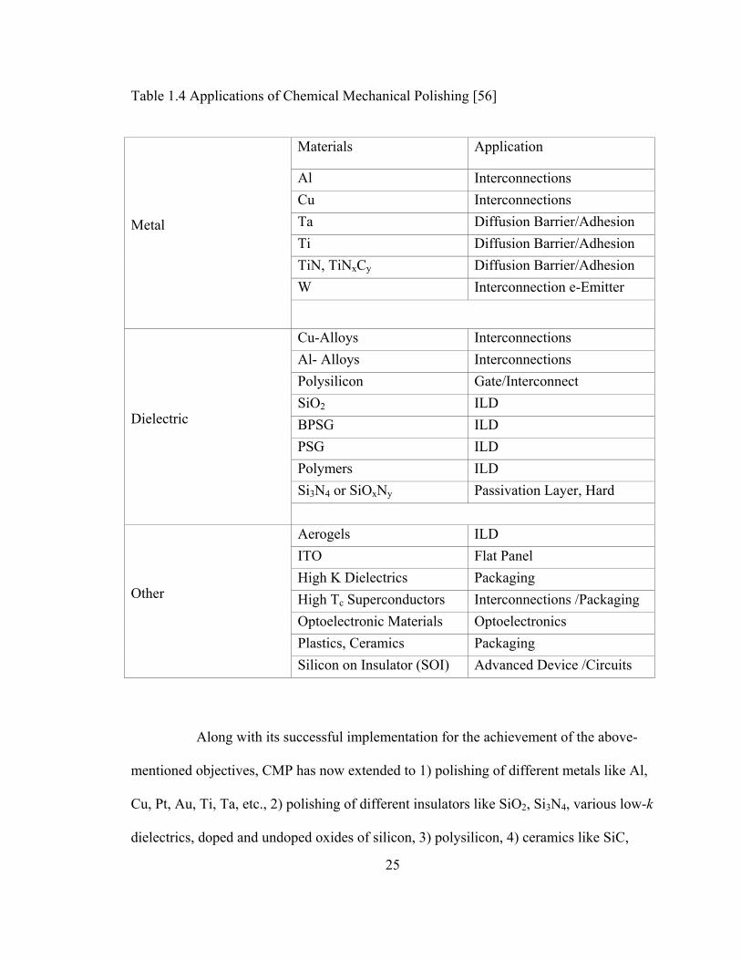
Table 1.4 Applications of Chemical Mechanical Polishing [56]
Materials Application
Al Interconnections Cu Interconnections Ta Diffusion Barrier/Adhesion Ti Diffusion Barrier/Adhesion TiN, TiNxCy Diffusion Barrier/Adhesion W Interconnection e-Emitter
Metal
Cu-Alloys Interconnections Al- Alloys Interconnections Polysilicon Gate/Interconnect SiO2 ILD BPSG ILD PSG ILD Polymers ILD Si3N4 or SiOxNy Passivation Layer, Hard
Dielectric
Aerogels ILD ITO Flat Panel High K Dielectrics Packaging High Tc Superconductors Interconnections /Packaging Optoelectronic Materials Optoelectronics Plastics, Ceramics Packaging
Other
Silicon on Insulator (SOI) Advanced Device /Circuits
Along with its successful implementation for the achievement of the above-
mentioned objectives, CMP has now extended to 1) polishing of different metals like Al,
Cu, Pt, Au, Ti, Ta, etc., 2) polishing of different insulators like SiO2, Si3N4, various low-k
dielectrics, doped and undoped oxides of silicon, 3) polysilicon, 4) ceramics like SiC,

26
TiN, TaN, etc., 5) multichip modules, 6) packaging, 7) optoelectronic components, 8) flat
panel displays, 8) microelectromechanical systems (MEMS), and 9) magnetic recording
heads and CD read write drives [56].
1.9 Overview
This dissertation begins with the need for device scaling and implementation
of novel materials in the present day semiconductor industry. The importance of
planarization and the various available planarization techniques with emphasis on CMP
have been discussed in Chapter 1. Chapter 2 gives an overview of the CMP process in
general and gives the background of the process and equipment used to carry out the
process. The different types of equipment used for CMP process and innovations there in
have been discussed in this section. The CMP findings of the studies involving in-situ
metrology of CMP and detection of process end point, slurry selectivity, as well CMP
defects using the CETRTM CMP tester have been discussed in Chapter 3. Chapter 4
elaborates the various issues surrounding integration of Cu and novel low dielectric
constant materials in the next generation damascene structures. The investigation of
specific gravity non uniformities and the use of application specific pads with novel pad
architecture have been discussed in Chapter 5 and 6 respectively. The investigation of
CMP slurry and synthesis of novel nanoparticle based Cu CMP slurry has been dealt with
Chapter 7. Finally, Chapter 8 summarizes the research, highlights significant
contributions and gives an idea of the future directions in which CMP is heading.

27
CHAPTER TWO
BACKGROUND OF CMP
3.1 Evolution of chemical mechanical polishing
By definition, chemical mechanical polishing is a process whereby a chemical
reaction increases the mechanical removal rate of a material. CMP is mostly used for
material removal by polishing the “hills” on the wafer and “flattening” the thin film. The
chemical reaction between the slurry and wafer is tailored to enhance material removal
and bring about quicker planarization of the thin film.
2.1.1 History of CMP
The modern day application of CMP process in the semiconductor industry
was for polishing the surface raw silicon wafers to achieve a global flatness over raw
silicon wafers. After sawing, the single crystal silicon rod and removing the mechanically
damaged surfaces, the wafer needs to be flattened globally and a uniform scratch free
surface needs to be made available for fabrication of semiconductor devices. The idea of
using colloidal silica, then made by Monsanto, instead of standard abrasives, was
developed by Bob Walsh in 1961 [59] and thus, the first wafers polished using CMP were
commercially available in the early 1960s [59, 60]. Before its implementation in
polishing raw single crystal silicon wafers, the process of CMP was traditionally used in

28
glass polishing. One of the most wide spread application of CMP outside the
semiconductor industry is optical lens polishing. In fact, the first machinery used by
Monsanto was very similar to the commercial machine used in the optical industry. The
first semiconductor CMP machine was an innovation of the optical lens polishing
machine. The proper polishing abrasives in presence of the slurry chemicals were used to
achieve a superior degree of precision and flatness to meet the demands of the
semiconductor industry. By supplementing mechanical polishing with high hardness
abrasives such as silica in an alkaline medium, there are significant gains in material
removal and reduction the process time.
A further improvement to the CMP process was made at IBM in the late
seventies and early 80 s. The new process was faster than the previous silica-based
polishing method and resulted in ultra flat, ultra smooth surface to meet the stringent
requirements of the IC industry [61]. The slurry was later tailored to reduce defects and
surface non-planarity introduced by the etching and deposition processes.
The IBM process was then applied for trench isolation by the late 1980s in
Japan for various logic and DRAM devices. There was wide spread industrial
implementation of the different variants of the CMP by companies such as NEC, National
Semiconductor, Hitachi, etc. This led to the introduction of the first commercial polisher
designed specifically for CMP by Cybeg in Japan in 1988. Later, International
SEMATECH identified CMP as a technology critical for the future of IC manufacturing
and launched a project to develop competitive, advanced CMP tools in the US [62].

29
2.1.2 Road Map of CMP Process
The semiconductor industry has effectively adapted its CMP technology for
the 300 mm wafer [63]. Beyond the adoption of copper interconnects, several
technologies are necessary to continue the shrinkage of device dimension and the
increase of packing density in ULSI manufacturing. The use of ultra low-k materials as
interlayer dielectrics has been at the forefront for decreasing the “C” of the “RC delay”.
However, polishing of ultra low-k dielectrics which are soft mechanically and weak is a
daunting task in itself. The single and dual damascene structures comprising of ultra low-
k porous or polymeric materials are more prone to buckling and crushing failures. It can
be seen from Table 2.1, that these materials have significantly lower hardness and
Young's modulus as compared to silicon di oxide which has a dielectric constant of about
3.2–4.0 available in the market today. According to the ITRS roadmap [14] materials
with dielectric constant 2.2 will be integrated in the IC by year 2007 (Table 2.1). The
difference between the polishing rates of copper and the low-k materials available will
significantly affect post-CMP surface planarity. New processes must be developed to
address the problems associated with this non-uniform polishing phenomenon as well as
the complexity of the materials structures. Also, there needs to be a marked improvement
in slurry selectivity for accurate end point detection when the constituent layers of the
damascene structure namely, metal, hard mask, cap layer, barrier layer and dielectric are
polished [64]. Furthermore, it is necessary to explore the niche of the CMP process in
shallow trench isolation and other applications such as backside polishing and the
fabrication of micro-electro-mechanical systems (MEMS). The CMP process there must
be integrated horizontally and vertically to achieve high thorough put and performance.

30
Table 2.1 Interconnect International Technology Roadmap for Semiconductors [14]
In MEMS applications horizontal integration ensures reliability and good
performance of a specific CMP process run. The development of new polishing pads and
pad architecture, novel slurries, new metrology techniques, etc. comes with in the scope
of horizontal CMP integration. Vertical integration ensures success of every successive
CMP operation. This includes the integration of the upstream processes such as
Cu/barrier deposition and etching and downstream processes such as ILD deposition and

31
lithography. This opens a wide scope for research for further optimization and
development of Cu CMP process.
3.2 CMP: A Multi-stage Process
Fig. 2.1 Flow Chart of the Isolated Industrial CMP Process
The recent developments in the semiconductor industry described previously
imply that CMP is fast becoming the established technology for planarizing metal and
interlayer dielectrics of multilevel sub-0.5 µm devices. Along with the rapid growth of
CMP and its application for polishing various materials, have come a variety of slurries,
different pads, complex process recipes, more complex slurry mixing and distribution
systems and an increase in the volume of wastewater. Polishing of different materials and
customized needs of the various semiconductor industries have given birth of more
complex CMP equipment with different process dynamics such as linear, orbital and
fixed head machines. Reliable filtration and waste distribution are also required to avoid

32
hazardous environmental implications, as the increase in the number of CMP process
steps have given rise to a large amount of disposable slurry waste. The schematic of the
industrial CMP process (isolated from the other process in the fabrication line) is as
shown in Fig. 2.1.
As seen from Fig. 2.1, the slurry is mixed in a tow at a central location from
where it is distributed to the various CMP machines in the fabrication. The slurry that not
used for feeding any machines is then returned back to the tow for recirculation. The
slurry that is used for CMP process is later disposed off. The wafer which is dry from the
previous process is loaded in the CMP process equipment where it undergoes polishing
and then cleaning. It is then dried in the CMP cleaning station (which may be integrated
with the polisher). Most machines follow this dry in dry out methodology.
2.2.1 Slurry Mixing
CMP slurry feeder equipment is composed of a stock solution unit, a mixing
and circulation unit, and the CMP equipment. The thick slurry supplied from the stock
solution unit is diluted to a fixed density in the mixing and circulation unit using ultra
pure water. The mixed and diluted solution is then supplied to the CMP equipment. All of
the equipments are manufactured in a clean room with high degree of cleanness, under
strict quality checking. Consistent construction method is used from the manufacturing of
the slurry feeder unit to local piping, wiring, cleaning and the trial run adjustment of the
system. The system thus needs to be of high quality and stability. A tolerance of about
1% is maintained in meeting the recommended slurry parameters. The schematic of the
slurry mixing is shown in Fig. 2.2. In this section, the various physical aspects of the

33
CMP process are discussed in detail in order to give a better understanding of the general
working of the industrial CMP process and the various parameters associated with it [65].
Fig. 2.2 Schematic of CMP Slurry Distribution System
2.2.2 Slurry Distribution
Fig. 2.3 gives a simplified physical representation of a semiconductor
fabrication line in which, the slurry distribution to the various CMP tools is shown. As
seen from the diagram, the slurry is mixed and blended at a centralized location from
which it is distributed to the various machines through the distribution lines. The
distribution loop shown in the schematic ensures that the “good” slurry, which is unused
for the process, is delivered back the mixing chamber or the tow, in order to prevent
slurry wastage. Although CMP slurries are composed of very fine particles up to 200 nm
(0.2 µm), “large” particles of 1–3 µm and greater are often present in slurries at the point
of dispense. Such particles can be formed as a result of agglomeration or the presence of
foreign material. Metal CMP slurries, in particular, are prone to formation of aggregates.
The agglomerated slurry particles often cause numerous defects in the wafer during
CMP. Microscratching is the most prominent defect which occurs mainly due the
agglomerated particles present in the slurry delivered to the machine as well as such
particles embedded in the pads [67]. This makes the continuous mixing of the slurry in

34
the tow absolutely imperative. In order to prevent the particle agglomeration [67] during
the distribution stage, dispense filters are installed on each of the machine which filter out
the agglomerated particles before slurry delivery. Care must be taken that the filtration of
the agglomerated particles does not change the particles distribution and concentration of
the slurry. Most often, a series of filters are used in order to minimize the drop in the
slurry pressure and flow. The slurry after being used for the actual CMP process in the
tool is then disposed off using appropriate methods and environmental damage is
restricted [68].
Fig. 2.3 Schematic of CMP Slurry Distribution System [68]
2.2.3 Working of the CMP Process
Current semiconductor fabrication technology for logic and memory devices
requires CMP to achieve the required multilevel interconnections densities. Indeed, each
silicon wafer can be exposed to 15 or more CMP steps before final device assembly. A
schematic diagram of the CMP process is shown in Fig. 2.4. During CMP, the wafer is

35
pressed face down against a rotating polishing pad, while a chemically and physically
(abrasive) active slurry planarizes the wafer. As wafer size grows, devices sizes shrink
and process requirements grow more stringent, within die/wafer uniformity and removal
rate increase becomes a greater concern. Different CMP processes attempt to achieve a
balance between removal rate and global/local planarization through a combination of
solution chemistry, speed, applied pressure and pad properties [56, 65]. Often a change in
slurry or operating conditions lead to conflicting performance.
Fig. 2.4 Schematic of Wafer Planarization by CMP Process

36
2.2.4 CMP Polisher considerations
The key issues affecting industry use of CMP during the semiconductor chip
manufacturing are the high cost of ownership (CoO), the lack of industry wide CMP
technology and less than thorough understanding of the knowledge of the underlying
science behind the CMP process [65]. Improvement in CoO has been brought about in
the fast few years due to: 1) higher raw throughput, 2) in situ film thickness metrology, 3)
dry in dry out configuration ensuring low defectivity [68], and 4) process equipment,
implementation and integration support from CMP vendors [68].
The first generation CMP tools based on rotational platen had low throughput
values of about 10–18 wafers/h [65]. The second generation tools emphasized on
evolutionary improvements while the third generation equipment designs were modified
to stay in production for long period of time by giving them adaptability to future
technology modifications. The throughput of the machine can be enhanced by increasing
the removal rate and improving the wafer handling. However, for effective CMP of
materials, the increase in removal rate by increasing the down force should not be
brought about by compromising on the defectivity (like increase in wafer to wafer and
within wafer non-uniformity, delamination, dishing, erosion, etc.) [70, 71] of the wafer.
For this reason sometimes, the throughput is compromised to polish the wafers at lower
down force there by increasing the polishing time [72].
2.2.5 First Generation CMP Polisher
The first generation CMP polishers use a single robot system to move the
wafer and hold it on the carrier. The polisher is comprised of two rotating platens; one

37
covered with a hard pad for bulk material removal and other with relatively soft pad for
buffing. The wafer is pressed face down on the pad by the carrier and the slurry is
deposited close to the center of the pad, from where the centrifugal force spreads it all
over. The mechanical properties, surface morphology, structure, absorbency, etc. strongly
affect the slurry distribution and polishing [73]. The polishing platen on these tools is
around 22 in. in diameter which is more than 7.5 times the size of a 200 nm wafer [65].
The actual slurry utilization of these processors is poor and the pH of the slurry changes
during use as there is an absence of any slurry reprocessing unit [74]. The amount of
slurry that is actually used for processing at the interface is function of pad properties
[75], pad conditioner [76], pad topography [77] and slurry viscosity [78]. Thus, the pads
must be conditioned to: 1) bring the pad back to flat, 2) remove materials from pores, and
3) rebuild the nap. Simple manipulation of the machine parameters is sufficient to
increase the material removal rate in these polishers. However, issues such as platen
wobble need to be taken care off in order to deliver CMP wafers in the acceptable range.
The schematic of the first generation polishers is similar to that shown in Fig. 2.5.
2.2.6 Second Generation CMP Polishers
The second generation polishers like, are basically made of rotating carrier
and platen designs but have numerous changes to improve the raw throughput. The
second generation polishers can be classified broadly in two distinct types: 1) single large
(22 in.) platen polishing numerous wafer concurrently on the same pad, and 2) single
wafer per platen, multi-platen systems [65].

38
2.2.6.1 Multi-wafer Per Platen Polishers
There is a natural increase in the throughput due to the increase in the number
of polishing heads per platen. However, this approach presents several challenges. The
most severe issue is the quantity of the wafer put at risk at one time. If one wafer breaks,
the pieces can damage several wafers at one time. The more subtle issue is that of load
balancing. As long as all the carriers on the platen are loaded with wafers, polishing can
be consistent. However in certain cases, like application specific integrated circuit
(ASIC) fabrication where in just one or two wafers need to be polished at one time, this
issue is of considerable importance. The schematic of multi wafer per platen polisher is
shown in Fig. 2.6.
Fig. 2.5 Photograph of Speefam (Novellus) Multi Wafer per Platen Polisher [78]
2.2.6.2 Sequential Rotational Systems
Another approach usually adopted to avoid the risk of damaging more number
of wafers due to pad anomalies is sequential polishing of wafers on different platens. This

39
approach involves multi-step polishing wherein the first platen is used for bulk material
removal without particular regard to superficial surface defects; the second platen is used
for global planarization while the third platen is used to for a fine buff to get a defect free
mirror like surface. However, synchronization of all these processes is an issue that the
process engineer needs to tackle with this approach. This implies the process speed is
limited by the slowest process. This is especially a problem when polishing metals such
as copper as the corrosion might results due to the wafer staying wet in the slurry for a
longer duration of time [79, 80]. Also, small damage to the pad can result in damage to
all wafers in the sequential polishing run and it is sometimes hard to determine the
damage on the pad and hence, all pads need to be changed. In case of tool failure, all the
processes need to be stopped until repairs and tool utilization is limited due to tool
inflexibility. Fig. 2.7 shows an illustration of sequential rotational CMP polisher.
Fig. 2.6 Applied Materials Inc., Sequential Rotational CMP Polisher (Courtesy: Ashok
Das, Applied Materials, Inc., Santa Clara, CA) [69]

40
2.2.7 Third Generation CMP Polishers
The third generation polishers have a series of evolutionary and revolutionary
systems built in them or integrated in them as modules. Dry in dry out feature is one of
the most prominent enhancements in this kind of polishers. This considerably reduces the
wafer defects especially in metal CMP as corrosion of the metal is drastically reduced as
a result of cleaning after the polishing step. The addition of in situ metrology modules
such as motor current detection [81], sensor array for integrated steering [82], thin film
reflectivity [83] in situ optical end point detection method [84] have markedly improved
CMP process performance and reduced defectivity. There are several new end point
detection and other metrology modules such are integration of acoustic emission sensor
[85], force sensor [86] and Cu radioactivity detection [87] that are candidates for
implementation in the third generation polishers.
2.2.7.1 Sequential Linear Polishers
The sequential linear third generation polishers are generally used in CMP for
STI and rarely in ILD structures. The polishers have a moving belt on which the wafer is
pressed device side down and rotated slowly about the carrier axis. The belt which is held
in tension between rollers moves rapidly [88]. This type of polisher can achieve high
removal rate owing to high belt speed and can achieve faster planarization as for STI
application where large amount of material needs to be removed from a relatively lower
pattern density structure. The low down force and high relative velocity polishing regime
limits the damage to the film [13]. The linear polishers require new set and architecture of
polishing pads which comprise of single polyurethane belt without foam or felt (sub-pad).

41
The concurrent polishing pad conditioning is obtained by means of a novel polishing pad
design where polishing pads have to be mounted in a cylindrical configuration and not on
a the conventional flat surface configuration [89]. A special polishing pad conditioner is
provided to refurbish the polishing pad [90]. With more and more publication of data
showing improved CMP performance at low down force and high linear velocity, this
type of polisher is finding increasing acceptance in the semiconductor processing
industry. Fig. 2.8 shows a photograph of a sequential linear polisher.
Fig. 2.7 Photograph of Sequential Linear Polishing System [97]
2.2.7.2 Orbital Polishers
Several CMP tool concepts have been developed based on orbital motion.
Some orbit the carrier with rotating the carrier [91-93] while others orbit the platen while
rotating the carrier [94]. Some of the polishers also involve arbitrary non rotational
motion on a fixed polishing pad. In these types of polishers the fundamental principle of
relative motion between the wafer and pad to remove the material is used, however,

42
unlike the first generation polishers, slurry is delivered directly at the pad area used for
polishing thus improving slurry utilization efficiency. The schematic of the orbital
polisher is shown in Fig. 2.9. The preferred mode of operation of orbital polishers is low
down force with high relative velocity. With the recent popularity of the contact retaining
ring method for polishing, the pad remains compressed at the edges of the wafer and
reduces the area of the die lost due to edge exclusion [95]. The planarization capabilities
of these tools are known to be better than the first and second generation polishers. These
of machines are also known for their small down times due to the rapid change individual
polishing heads.
Fig. 2.8 Schematic of Rotary CMP Polisher [13]
2.2.7.3 Rotary Inverted
Recently, Nikon Inc. has developed high-precision CMP systems applying
proprietary technology based on its long experience in lens polishing and optical
measurement [96]. The system's special face-up polishing uses small pads applied at very

43
low pressure and high-speed rotation. The compact polishing pad as seen in (Fig. 2.10 a)
enables high-speed rotation. Its light-weight, less pad deformation feature allows superior
planarity. These features are especially advantageous ultra low-k polishing process.
Through the compact polishing pad the slurry is supplied onto polishing area of the wafer
efficiently. This enables less slurry consumption compared to the conventional polishing
equipment (Fig. 2.10 b). Face-up polishing at the polishing station enables continuous
optical end-point measurement. It helps improve S/N ratio while minimizing slurry effect
for end-point detection. Mounting of wafer and pad are also convenient with this system.
In spite of some initial excitement about this system, it is yet to have a proven track
record in the semiconductor fabrication environment.
Fig. 2.9 a) Set up of Multi Wafer Rotary Inverted CMP Polisher and b) Polishing Action
and End Point detection [96]
2.2.7.4 Pad feed Polishers
The pad feed polishers are based on a recently developed pad type that is held
in rolls. These polishing pads are fed to the wafer polishing tables, the wafer is polished,

44
pad is conditioned and then the pad moves further (Fig. 2.11). This methodology is
especially useful for pads that have very repeatable first polish performance and their
characteristics either degrade or change with subsequent polishing runs. This polisher
unlike others does not have to be turned off for changing the pad there by maximizing the
equipment utilization time [97, 98]. This technology is still in its nascent stage and
various industrial giants continue to develop it even further in order to make a positive
impact on the CMP polisher market.
Fig. 2.10 Schematic of a Web-type Polisher [98, 99]
3.3 Physics of CMP Process
In 1927, the Preston equation was developed (Eq. (2.1)) [99], for modeling the
mechanical effects of pressure and velocity in the CMP process:
R=KPV (2.1)

45
where R denotes the polish rate, P is the applied downward pressure, V is the linear
velocity of the wafer relative to the polishing pad, and K is a proportionality constant,
called the Preston coefficient. As seen in Fig. 2.12 rcc is the linear distance between the
centers of the wafer carrier and the platen, which is mostly assumed to be constant, rH (H
stands for head) is the positional vector at any point Q on the wafer from the center of the
carrier and this varies with the position of the point Q, rth is the positional vector of any
point Q on the wafer from the center of the platen (this distance varies with the location
of Q). VQ is the velocity of any point Q on the wafer. VT and VH are the linear velocities
of the table (platen) and wafer head. ωT, ωH are the rotational velocities of the platen and
wafer carrier. Assuming that ωT ≠ ωH velocity VQ will vary from point to point over the
wafer. The variation in velocity will call cause changes in the removal rate across the
wafer in accordance with the Preston's equation.
rth=rcc+rH (2.2)
VQ=VT+VH=−(ωT×rT)+(ωH+rH), where VQ=(ωT×rcc)=[rH(ωT−ωH)] (2.3)
Fig. 2.11 Schematic of the Force Field on the Wafer and the Pad during CMP [37, 70]
However, if ωT is set equal to ω then linear velocity will be independent of the
location of the wafer for VQ = −[ωT × rcc]. This with the VQ maintained as shown before,
the velocity of all points on the wafer will be the same and then there will be no change

46
in the removal rate of the material. This force field analysis is taken in to account to
fundamentally design any CMP process [37, 70]. In any event, many times, the process
engineers are still confronted with the problem of wafer to wafer and within wafer non-
uniformity (WIWNU and WTWNU) (Fig. 2.13) [33].
Fig. 2.12 Non-uniformity in Removal Rate with in a Wafer [33]
3.4 Parameters Governing CMP process
The physical forces acting upon the wafer govern only a part of the entire
tribo-chemical phenomenon of CMP. The process of CMP is governed by various input
variables that act on a micro as well as nanoscale to produce desirable or undesirable
output parameters. The interplay and interaction of different micro and nanoscale
parameters takes place sequentially or simultaneously, predominantly at the pad wafer
interface, during the entire CMP polishing run. Though machine parameters when input
in the Preston’s equation may appear to be the dominant in any CMP output, the entire
governing dynamics of industrial scale CMP is much more complex. Fig. 2.14 is an
attempt to correlate the various parameters in the CMP governing dynamics.

47
Fig. 2.13 Parameters Governing the CMP Dynamics [101]

48
3.5 Research Objectives
The broader objective of this research is to understand the process of CMP
which has been more of an art that science. The specific objectives, milestones and
subjects of investigation along with the expected outcome are shown in Fig. 2.15.
Fig. 2.14 Schematic Showing Objectives of the Current Research
Study of CMP Process
Investigation and Modification of CMP Pads 1. Evaluation of Pad material properties 2. Evaluation of pad non uniformity 3. By-passing Pad conditioning 4. Making Pad specific to Polishing Application 5. Tribological Evaluation of Pad 6. Determination of Polishing Pad Architecture
Effect of Machine Parameters 1. Variation of down force 2. Variation of Linear Velocity (Platen Speed and Carrier speed)3. Variation of Slurry flow 4. Defect Detection and Process Optimization
Investigation and Modification of CMP slurry 1. Evaluation of Slurry Frictional Performance 2. Slurry selectivity 3. Removal Rate 4. Overall slurry performance 5. Introduction of surface catalyst
Material Aspect of CMP1. Material Inspection 2. Mechanical Properties 3. Interfacial Adhesion 4. Pre-CMP material Characterization 5. Material Tribological Properties
Contribution towards CMP Process Module Development
Investigation and Modification of Chemical Mechanical Planarization
Consumables

CHAPTER THREE
METROLOGY OF CMP
3.1 Need for Effective CMP Metrology
The CMP process combines mechanical and chemical removal mechanisms in
a synergistic effect. This synergy has been the subject of many studies, but focus in the
past has been primarily on mechanical effects due to the difficulty of identifying the
reaction mechanisms of the chemical effect. However, mechanical effects alone cannot
provide the type of polishing necessary for IC manufacturing. Chemical effects contribute
to the increased global planarity and reduced micro roughness required for successful IC
fabrication. As discussed in the earlier section, the fundamental basis for designing any
CMP process module, the force field analysis of the wafer–pad–slurry abrasion system is
made. The variations in the machine parameters to obtain optimal results are the first
adjustments made to refine the CMP process. Until recently, slurry flow and slurry flow
rate was not given much importance variation of machine parameters [65], however, with
the ever-growing demands for enhanced yield and low defects, and also with the
knowledge of the heat transfer behavior of the slurry [100], the slurry flow is also brought
in the CMP process control equation. This section discusses the broader impact of these
machine parameters on the CMP process. A better understanding on the effect of machine
parameters on the CMP process can be obtained by performing repetitive CMP

50
experiments on a prototype CMP tester in which process data is monitored in situ. We
have used the CETR bench top. for studying the CMP process in detail. The details of the
CMP tester are described below and also can be obtained in literature [102].
3.2 CMP Tester
Most of the CMP processes during this research were performed on a CMP
tester (CETR, Inc, CA) with variety of process parameters. A photograph of the tester is
shown in Fig. 3.1. The lower platen can hold a pad up to 6” in diameter. The upper
carriage can hold two inch wafers or sample coupons up to 1.5” X 1.5”. The upper
carriage can rotate about its own axis and oscillate radially with the pad during
planarization process. A strain gauge force sensor (0-200 N) can record both vertical and
friction forces and hence co-efficient of friction (COF) is monitored during the process.
The system is also equipped with a high frequency acoustic emission sensor. AE-
Analysis is an extremely powerful technology that can be deployed within a wide range
of usable applications of non-destructive testing: metal pressure vessels, piping systems,
reactors, and similar. All solid materials have certain elasticity. They become strained or
compressed under external forces and spring back when released. The higher the force
and, thus, the elastic deformation, the higher is the elastic energy. If the elastic limit is
exceeded a fracture occurs immediately if it is a brittle material, or after a certain plastic
deformation. If the elastically strained material contains a defect, e.g. a welded joint
defect, a non- metallic inclusion, incompletely welded gas bubble or similar, cracks may
occur at heavily stressed spots, rapidly relaxing the material by a fast dislocation. This
rapid release of elastic energy is what we call an AE event. It produces an elastic wave

51
that propagates and can be detected by appropriate sensors and analyzed. The impact at
its origin is a wideband movement (up to some MHz). The frequency of AE testing of
metallic objects is in the range of ultrasound, usually between 100 and 300 kHz. The
acoustic emission sensor employed in this tester has a frequency range between 0.5 to 5
KHz. The AE sensor, in conjunction with COF, has been used to detect the delamination,
endpoint, and debris during polishing (described later) during the course of this research.
Fig. 3.1 Photograph of the CETR CP-4 CMP Tester
The state-of-the-art CMP tester is a testing tool and thus the following
assumption are made when different pads, slurries and materials were evaluated: 1)Due
to the lack of uniformity on the surface of the coupon, an average of the material removal
rate measured at different points from the center to the edge was assumed to be the MRR
Pad with Lower Platen
Slurry Flow
Slider Assembly Force Sensor
Upper Carriage
Slurry Outlet

52
of the polishing run, 2)During the in-situ detection of MRR using COF and AE, the non
uniformity of the sample surface brought about gradual tapering of the signals even for
blanket samples. The end point was assumed to have occurred when more than 70 % of
the material was removed from the surface and further material removal brought
insignificant change in the AE and COF signals.
3.3 Coefficient of Friction (COF) and Material Removal Rate (MRR)
To understand the variation of COF and MRR, which are the primary output
variables of any given CMP process, the polishing tests on the CETR tribometer. The
samples used in this case were 1 in. × 1 in. PECVD SiO2 using Klebesol 1501 (Rodel
Inc., DE) colloidal silica slurry (pH 10–11) on an IC 1000/IV pad with linear velocity
5 mm/s and a radial distance of 50 ± 2.5 mm. The down force used was 4 PSI and the
platen rotation was 150 RPM. Influence of machine parameters such as down force,
relative velocity, slurry flow on the acoustic emission (AE), coefficient of friction (COF)
and material removal rate (MRR) was observed. For removal rate calculations, thickness
of oxide was measured at nine points using the ellipsometer. The wear rate was
calculated by re-measuring the sample after polishing at nine points.
COF is an important tribological property of films and pad as it gives an
estimate of the surface shear which directly affects the MRR. The COF was recorded
during all the tests. Fig. 3.2 (a, b) shows the COF versus RPM and PSI, respectively,
during polishing. With higher RPM, COF decreases, whereas, decrease of COF is very
small with the increase of PSI.

53
Fig. 3.2 a)Variation of COF with RPM (platen velocity) for Different Values of Down
Pressure (PSI), b) Variation of COF with PSI (Down Pressure) with Different Values of
Platen Velocity (RPM)
Fig. 3.3 a, b shows the variation of MRR as a function of RPM and PSI,
respectively. Experiments on two sets of samples show the same trend. Removal rate
increases with both RPM and PSI. Removal rate decreases slightly at platen rotation
250 RPM. This may be due to inadequate slurry flow under the sample at higher platen
rotation. As COF decreases with increasing RPM and PSI, a lower COF may be related to
the higher removal rate in CMP process. Fig. 3.4 shows the removal rate versus RPM ×
PSI and the linear relation indicates that polishing of oxide follows Preston's equation
[99].

54
Fig. 3.3 a) Variation of Average Removal Rate with RPM at Different Down Pressure
(PSI) for the Evaluated Set of Samples, b) Variation of Average Removal Rate with PSI
(Down Pressure) at Different Platen Velocity (RPM) for the Evaluated Set of Samples

55
Fig. 3.4 Average Material Removal Rates Plotted with RPM × PSI. Linear Relation
Indicates that Polishing Follows Preston's Equation
3.4 Importance of Slurry Flow
It is important to optimize the effect of slurry flow rate on the COF and AE
signal. Results of the optimization experiments are summarized in Table 3.1. It can be
seen from Table 3.1 that COF decreases slightly while no significant change can be
noticed in AE signal. Decrease of COF may be attributed to the higher slurry flow rate
during polishing. Therefore, the data suggests that flow rate may not affect the AE signal.
The flow pattern of the slurry on the pad affects the polishing rate as well as the
WIWNU. Due to the rotation of the lower platen the flow pattern will be different as we
feed the slurry at different positions of the pad. Fig. 3.5 shows the different positions of
slurry feeding on the platen. If the slurry cannot reach uniformly at the pad-film contact
points material will not be removed uniformly. It can be seen from Fig. 3.6 that center

56
position and position “8” (very near to the center) are two better positions to feed slurry
while platen is moving clockwise.
Table 3.1 Effect of Slurry Flow rate on COF and AE
Run # Slurry flow (ml/min) COF AE signal (arbitrary unit)
1 35 0.3977 0.4013
2 75 0.3949 0.4533
3 100 0.3932 0.4184
4 155 0.3911 0.4133
5 195 0.3888 0.4189
Fig. 3.5 Schematic of the Positions of Slurry Feeding on the Pad during Polishing for
Feeding Position Optimization; Distance 0–1.4 = 15 mm, 0–2.5 = 30 mm, 0–3.6 =
45 mm, 0–7.9 = 45 mm and 0–8 = 25 mm
The friction generated during CMP brings about over all increase in the
temperature at the wafer pad interface. Certain CMP processes such are silicon polishing
are exothermic. Hence, there is a natural increase in the temperature at the interface. The
increase in temperature changes the reaction kinetics of the slurry with the wafer, mostly
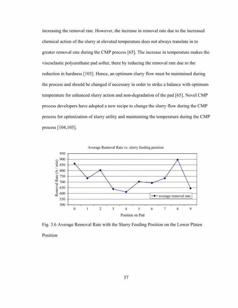
57
increasing the removal rate. However, the increase in removal rate due to the increased
chemical action of the slurry at elevated temperature does not always translate in to
greater removal rate during the CMP process [65]. The increase in temperature makes the
viscoelastic polyurethane pad softer, there by reducing the removal rate due to the
reduction in hardness [103]. Hence, an optimum slurry flow must be maintained during
the process and should be changed if necessary in order to strike a balance with optimum
temperature for enhanced slurry action and non-degradation of the pad [65]. Novel CMP
process developers have adopted a new recipe to change the slurry flow during the CMP
process for optimization of slurry utility and maintaining the temperature during the CMP
process [104,105].
Fig. 3.6 Average Removal Rate with the Slurry Feeding Position on the Lower Platen
Position

58
3.5 CMP End Point Detection (EPD)
The difference in removal rate of one material as compared to another in a
given slurry yields the measure of the selectivity of that slurry for those two materials.
Higher the slurry selectivity, the more effective is the end point detection for a particular
CMP process step as there is a marked change in the tribological properties of the
material being polished and the under layer. Selectivity is a very important criterion in
designing any slurry. For STI, slurry used needs to act on the oxide that is being
planarized and not act on the underlying nitride. For polishing Cu, the slurry needs to act
selectively on Cu and spare the barrier layer Ta and underlying layers of silica or low-k
dielectric material. Typically slurry selectivity of 10–25 has been reported for Cu
polishing [101]. The selectivity could be considerably improved up to 1000 by
introducing particle free slurry [106, 107]. The reduction in mechanical component due to
lack of abrasive implies that majority of material removal takes place due to solution
chemistry which can be made highly selective. Slurries with high selectivity facilitate
easy end point detection as the tribological properties of the material say Cu being
polished in a highly selectivity slurry are markedly different from the properties of the
barrier layer Ta or underlying silica layer when polished in the same slurry. The
difference in tribological properties can be monitored in situ using techniques such as
motor current or force and acoustic emission sensor.
The variation in coefficient of friction and acoustic emission for polishing of
blanket Cu, Ta and ultra low-k dielectric (k = 2.2) has been studied. The candidate
materials have been polished in the form of 1 in. × 1 in. coupons on the bench top CMP
tester (mentioned in Section 3.2) [102] to evaluate the selectivity of the slurry. The

59
slurries evaluated were: 1) Cu selective alumina particle slurry (Cu1), 2) Cu selective
particle less slurry (Cu2), 3) Ta selective slurry with colloidal abrasives (slurry Ta), and
4) non-selective slurry (slurry Cu–Ta). Fig. 3.7 a–d shows the variation of COF and AE
at 2 PSI and different platen speeds. It can be seen from the figure that the value of COF
for a particular material for one polishing condition is unique and hence monitoring the
value of COF can give an estimate of the end point of the process.
Fig. 3.7 a) Variation of COF at 2 PSI Down Force and Variable RPM in Slurry Cu1, b)
Variation of COF at 2 PSI Down Force and Variable RPM in Slurry Cu2, c) Variation of
COF at 2 PSI Down Force and Variable RPM in Slurry Ta, and d) Variation of COF at
2 PSI Down Force and Variable RPM in Slurry Cu–Ta [85, 86]
Just as the COF is a strong function of the down pressure, platen and carrier
velocity, and the choice of the slurry and pad, the acoustic emission during CMP is
already affected by the choice of the aforementioned CMP variables. The variation of

60
AE and COF for different materials polished in a commercial Cu slurry is shown in Fig.
3.8 a. It must also be noted here that the same materials displays different COF with
polished using different slurries. This can be seen from Fig. 3.8 b where different
materials, namely Cu, SiLKTM (ILD material) and Ta are polished in commercial slurries
named here are “Cu2”, “Ta” and “Cu-Ta”. The slurry Cu2 is selective to Cu while Ta is
selective to Tantalum. The slurry Cu-Ta is a non selective slurry.
Fig. 3.8 a) Variation of AE and COF for Different Materials Polished in a Commercial
Cu Slurry, b) Variation of COF for 3 Materials Polished in Three Different Slurries
0 0.5 1 1.5 2 2.5
Cu
Ta
Lowk B
Lowk C
SiC
SiO2
COF/AE
AECOF
0
0.1
0.2
0.3
0.4
0.5
0.6
0.7
0.8
0.9
1
Slurry Cu 2 Slurry Ta Slurry Cu-Ta
COF
CuSiLKTa
a
b

61
Addition of specialized chemicals that can act as catalysts in the chemical
interaction between slurry and the polished material there by increasing the rate of the
chemical reaction with the material being removed considerably is a common approach
for improving the selectivity of the slurry. Tetra-methyl ammonium hydrate (TMAH) can
be added to Cu slurries to considerably decrease silica polishing rate [108, 109].
Phosphoric acid added to alumina and colloidal silica TaN slurry has also shown
accelerated chemical reaction with TaN. Fig. 3.9 shows the increase in the polishing rate
of TaN with addition of phosphoric acid in alumina and colloidal silica slurry [110]. The
effect of surface catalyst in the slurry has been investigated and details have been
reported in later in this dissertation.
Fig. 3.9 Cu and TaN Polishing Results (Head 40 RPM, Table 40 RPM, and Pressure
7 PSI) [110]

62
Among the several different models proposed for friction and interfacial heat
dissipation, pad-wafer interactions during CMP tend fall in the molecular friction model
at a nanoscale. The molecular friction model essentially postulates that when two
different surfaces come in contact, the imbalanced Van der Vaal forces of the surface
molecules results in adhesion or “stiction” between the two interfaces. It must be
mentioned here that if one of the surface is significantly rougher than the other (as is the
case with CMP when pad is significantly rougher than the polished wafer), macro-scale
parameters such as “asperity lock-in” also govern the friction phenomena. In the event of
an abrasive containing fluid present at the pad wafer interface, the overall energy required
to overcome the combined effect of the Van der Vaal’s interaction of pad, slurry and
abrasive materials with the polished wafer. Hence, the choice of the polished material,
polishing pad, and CMP slurry will directly influence the friction force and hence the
COF at the pad wafer interface during polishing. This interaction of the different
aforementioned materials will also impact the strain to which the material subjected to
during polishing at the given polishing conditions. The strain and the strain relaxation
which is the root cause of the elastic wave sensed by the AE sensor will thus change for
different process recipes and parameters. Upon complete removal of polished material,
the exposure of the material underneath will change one of the variables (the polished
material) in the interactions taking place at the interface of pad and wafer. This will in
turn affect the COF and AE values measured in-situ. This principle could be used for
effective CMP end point detection. The time taken for complete material removal can
give an reasonable estimate of the material removal rate during CMP. If the polishing is

63
continued for sustained period of time, then the time taken for the complete material
removal of the buried layers can give an idea of the selectivity of the slurry.
3.6 In-situ Process Monitoring and Slurry Selectivity
The previous section described in-situ monitoring of CMP process of
predominantly blanket samples. However, in reality, wafers that undergo CMP have an
intricate pattern based upon the design layout. This gives many new paradigms to the
CMP process monitoring. However, the knowledge gained from in-situ process
monitoring of blanket samples can be used for studying the CMP of STI structures. The
variation in pattern density in the topography of the wafer can accentuate a special type
of defect known as ‘dishing’ [111, 112]. A schematic illustration of dishing and erosion
defects is shown in Fig. 3.10. This dishing effect is characterized by high polishing rates
in localized regions where the pattern is significantly different from its surrounding. The
formation of the trough shaped dish has been attributed to excessive over polishing in
these areas. Efficient end point detection (EPD) helps prevent these and numerous other
CMP defects.
Fig. 3.10 Schematic Illustration of Dishing and Erosion

64
The overview of the STI process has already been given in Chapter 1.
However, before the process monitoring of STI CMP is discussed, it is important to
understand the background and layout of the evaluated structures that would undergo
CMP. In STI structures, the field oxide is embedded in the Si wafer in order to clearly
separate the device active areas. This allows smaller device pitches and higher packing
density. Fig. 3.11 shows an SEM micrograph of the Focused Ion Beam (FIB) cross
section of an STI structure.
Fig. 3.11 SEM Cross-section of STI Structure
The process of the fabrication of STI structures (besides minor possible
process variations) is relatively well characterized and is already discussed in literature
[113]. Some of the teething challenges in STI process are: 1) effective trench oxide
filling, 2) thermal stability and wet etch resilience of the oxide, 3) with in die non
uniformity after CMP of field oxide, 4) incomplete polishing of the oxide, 5) oxide
dishing and nitride erosion, etc. Most of these STI process challenges can be resolved
Trench Oxide
Needed Step Height Reduction of field Oxide
Potential Active Device Area
Si3N4 Layer

65
using effective process EPD. It can be argued that during the polishing of STI structures,
the COF will change when the nitride layer is exposed after removal of field oxide.
In this study, we used the variation of COF during the CMP process for in-situ
EPD. CMP polishing run was carried out for an extended period of time to determine the
oxide and nitride MRR and oxide to nitride selectivity of the slurry. The surface of the
wafer was characterized ex-situ using Atomic Force Microscopy (AFM) before, in the
middle, and after process end point.
The evaluation of sample surface morphology was done using AFM in the
tapping mode. The surface morphology before polishing showed 3.5 µm X 3 µm
pedestals with 2 µm device area (Fig. 3.12). The AFM characterization was also
performed after partial removal of oxide during CMP as well as the complete removal of
field oxide. The process parameters specifically studied were: 1) variation of COF with
time, and 2) variation of material removal rate (MRR) for each material under different
polishing conditions. The details of the experiments are shown in Table 3.2.
Fig. 3.12 3D AFM Image of the Evaluated STI Structure with Step Height Measurement
Vertical Distance: 375.50 nm Horizontal Distance: 2.969

66
The COF, which is the ratio of the shear force (Fs) to the normal force (FN)
(N
s
FF
COF = ), is measured in situ during the process. When a patterned wafer (in this
case STI) is pressed face down on the surface of the polishing pad under a particular
value of down pressure, the pressure is distributed uniformly over the entire topography.
The density of the pattern thus strongly affects the local pressure on the surface of the
wafer. The step height reduction takes place at a brisk rate during the initial stages of the
CMP process due to the higher local pressure. As the material removal from the surface
of the wafer takes place primarily due to shear, higher shear force generated due to the
aforementioned mechanism is the cause of higher values of COF after carrier touch
down. The shear force also depends upon the chemically modified surface layer that
results due to the interaction of the surface and the slurry.
Table 3.2 CMP Experimental Details
# Parameter Conditions
1 Down Pressure 4 PSI for EPD experiments, 8 PSI for Slurry Selectivity
2 Platen Rotation 200 RPM Platen Rotation, 195 Carrier Rotation
3 Slider 35mm ± 5mm (position) @ velocity of 5 mm/ sec
4 Slurry ILD 1300 (pH~10.5) with colloidal silica abrasives
5 Pad Rodel, Inc. IC1000 Suba IV A4 perforated
6 Time of polishing Until Process End Point
7 Polishing Specimen 1” X 1” coupon

67
Fig.3.13 In situ Variation of COF during CMP Split in to Different Stages
In case of STI patterns being polished by ILD slurry designed to planarize
SiO2, the planarization chemical mechanism involves: 1) penetration of water in the
material surface in presence of an alkaline medium, 2) surface layer dissolution, 3)
removal of hydrolyzed material by particle impact, 4) Partial redeposition of dissolved
products, 5) reaction of surfactant on the abrasive on material removal [114]. Any change
in the material removal mechanism will cause the change in the nature of interactions at
the pad wafer interface. There is a drastic change in the slurry-surface interaction when
the Si3N4 layer is exposed after the removal of field oxide. In comparison with SiO2, the
hydroxylation of the Si3N4 surface is markedly reduced. Also, silicon nitride being
significantly harder than SiO2, the silica particles tend to roll over the surface due to the
slurry flow and show lesser tendency for indentation. This causes lesser shear for a given
down force, which in turn implies that COF values when Si3N4 is polished by silica ILD
slurry are lesser as compared to SiO2. However the COF measured during Si3N4 polishing
0 100 200 300 400 500Time sec
-1.5
-1.0
-0.5
0
0.5
1.0
1.5
COF-Ff 0.311758
163
del 105
Stage A
Oxide Polishing
Stage B
Nitride Polishing
Stage C
Nitride Removed
Oxide Removal Rate: ~ 400nm/min
Nitride Removal Rate: ~ 80 nm/min
Slurry Selectivity: 5:1
Process Conditions: 8 PSI/ 200 RPM (platen) -195 RPM (carrier)

68
is the combined COF of the Si3N4 pads and surrounding trench SiO2. Hence, though there
is a difference in COF value when Si3N4 is being polished, the magnitude of the COF is
not markedly different (Fig. 3.13). The COF value again changes when the Si3N4 is
completely removed and field oxide is polished. The CMP experiments were first
performed on 1”X 1” STI coupons at a down force of 8 PSI and 200 RPM platen/ 195
RPM carrier rotation for 500 seconds.
During the stage A, the COF continuously goes down after the initial high at
touch down. Another CMP process run was performed and stopped before completion of
Stage A. Based upon the previous discussion, it can be thus hypothesized that progressive
decrease of COF during the first stage corresponds to SiO2 material removal. As COF is a
characteristic of particular material for the given set of polishing conditions and
consumables, after complete removal of SiO2, and exposure on the nitride regions, there
is a change in the COF. This transition can be seen to reach after 58 seconds for the
polishing run reported in Fig. 3. 13.
For exposure of Si3N4, the step height of the oxide has to be removed, along the
surrounding excess field oxide. The height reduction was approximated to 400 nm and it
implied that SiO2 material removal rate (MRR) during the process run was approximately
to 400 nm and that implied that SiO2 material removal rate (MRR) during the process run
was 400 nm/ min. Further polishing of sample coupon showed that CMP of Si3N4
produced 80 nm/min MRR. Thus the oxide to nitride selectivity of the slurry at the given
process condition was found to be around 5:1. This selectivity ratio is in agreement with
the industry standards [115].

69
Fig. 3.14 Ex-situ 3D AFM Image of the Evaluated STI Structure with Reduced Step
Height before Termination of Stage A (ref. Fig. 3.13)
Fig. 3.15 Ex-situ 3D AFM Image of the Evaluated STI Structure after Process End Point
just after Beginning of Stage B (ref. Fig. 3.15)

70
Another polishing run was performed till the process end point was reached (ref
Fig. 3.13) and COF transition was observed. The sample coupon polished just until the
beginning of Stage B was characterized ex-situ using AFM as shown in Fig. 3.14. It can
be seen from Fig. 3.15 that, the nitride regions on the surface of the samples are exposed.
This shows that the CMP process has reached its end point due to the complete removal
of the field oxide. The “spikes” on the surface of the AFM 3D image are due to the
particle adhesion. The particles adhered to the surface due to non availability of an
efficient post CMP set up. The AFM section analysis shows a planar surface with and
surface variations can be primarily attributed to the surface roughness. The evaluated
COF during the entire stage B is a combination of the COF of nitride and oxide. With
progressive decrease of nitride layer during CMP, the value of COF tends to increase till
nitride is completely removed and oxide is exposed. To evaluate the repeatability of the
hypothesis, CMP runs were performed at different values of down pressure and platen
rotation. The data of the two of such trials performed at a down pressure of 4 PSI, 200
RPM platen rotation and 195 RPM carrier rotation is shown in Fig. 3.16. It can be seen
from the figure that the CMP process end point occurs at 200 sec. for both process trials.
Also the variation of COF follows a similar trend for both the trials. Thus it can be
inferred that for the given process conditions and parameters, the process end point is
reached at almost a similar time with in margin of acceptable error. The spikes in the
COF data could be attributed to the noise during data collection. In order to filter the
noise, obtained sharp transitions of end point, and study the “events” such as
microscratching, dishing, erosion etc., during the process, the COF data needs to be
further filtered using specialized signal processing filters. As the COF is data is non

71
stationary and even random to some extent (depending upon process defects or “events”),
the COF signal has to be filtered in time as well as frequency domain. Wavelet based
techniques have been found appropriate for sharp end point detection from using COF
[116].
Fig. 3.16 In-situ data for 2 Trial Runs Shown to Demonstrate repeatability
Thus, it can be concluded from this study that real time monitoring of the
CMP process can give valuable information which otherwise would need ex-situ
metrology for evaluation. The values of COF being the “signature” of a particular
pattern, material, pad, slurry and polishing conditions can be used as a fingerprint of a
particular STI CMP process run. The work could be further extended in evaluating
different pattern densities and different High Selectivity Slurries for STI CMP.

72
3.7 Delamination during CMP
The next generation low-κ materials are generally porous in nature and poor
adhesion of dielectrics in a stack may result in delamination during the CMP process.
Loading forces and rotation rates may also affect the reliability of the structure.
Delamination can occur due to either: 1) adhesive failure at the low-κ and barrier layer
interface, 2) failure within the low-κ material, or3) failure of the cap layer and low-κ
interface. The process conditions must be adjusted in such a way that the overall hardness
of the pad surface does not cause the aforementioned defects. It has been found that the
density and size of abrasives along with the CMP process conditions have a strong effect
on delamination during material planarization [117].
To understand and demonstrate the phenomenon of delamination, three
different types of materials namely: 1) Patterned Cu samples with low-k A (A) (k~<2), 2)
Patterned Cu samples with low-k B (B) (k~2.0), 3) Patterned Cu samples with SiO2
(TEOS) (k~4.0). Henceforth, these samples will be referred to as ACL, BCL, and TC
respectively. Small coupons (2cm X 2cm) of samples were used to polish on either 6” or
9.5” pad coupon at different rotation of platen (0.2 to 1.5 m/s) and down force (1-10 PSI).
Upper specimen was allowed to oscillate back and forth by 5 mm (47.5-52.5 mm) with a
speed of 1 mm/s. Polishing slurry was fed into the interface continuously with the rate of
55 ml/min. On some occasions, tests were stopped before 300 sec due to high vibration
and sample holder rotation. Slider movement for these experiments were 50±2.5 with a
velocity 1 mm/s. Slurry flow was fixed at 55 ml/min. Polishing pad was a perforated
IC1000/SubaIV while alumina based Cu selective slurry was fed continuously at the
center of the pad.

73
Fig. 3.18(a) shows the AE signal variation while polishing with active upper
rotation and Fig. 3.18 (b) shows the optical picture of the coupons after polishing. As it is
seen for the samples polished with non upper rotational machine, highest AE signal is
recorded for sample ACL and lowest signal for sample TEOS while a little smaller value
is recorded for sample B than sample A. As sample ACL consists of Cu-ultra low-k
samples with lowest k values, delamination may be more for this sample. It can be seen
from Fig. 3.18 (b) samples get polished more uniformly with an upper rotation whereas
samples gets more polished at the leading edge only for no upper rotation. From the
samples it could also be seen that all the ACL and BCL samples are delaminating
whereas TEOS has no sign of delamination.
0 50 100 150 200 250 300 350Time sec
0123456AE Volt
Fig. 3.17 a) Picture of Sample Coupons ACL, BCL, and TC after Polishing, b) Variation
of AE signal of Three Different Samples
Further analysis of the samples with SEM, shown in Fig. 3.18, reveals that
AB
TEOS
a
b

74
during the process Cu either gets peeled off or delaminated. Even delamination of
underlying interlayer dielectric films could be seen. In all conditions, and experimental
setups AE signal was higher for sample A and B than TEOS. Also, sample ACL
produced more AE signal than sample BCL. It is prudent to mention that the only
difference among the three samples is the underlying ultra low-k ILD film. High AE for
ACL and BCL sample may be an indication of delamination of Cu from barrier and ILD
interface. As Low-k B has slightly higher k values, which implies better mechanical
strength, sample B shows better resistance to the CMP process. Lower magnitude of AE
for sample BCL than sample ACL is the reason for this conclusion.
ACL 2 ACL 2 ACL6 BCL4 BCL 5 TC 12
Fig. 3.18 SEM Micrographs Showing of Delamination of Different ACL, BCL Samples
and No Delamination for TC Sample
Severe delamination or scratching on the surface could be monitored with the
AE sensor, which produces spikes during the unusual polishing. Two ACL samples were
run in the same conditions along with a TEOS sample. The expanded AE signals for all
three samples are shown in Fig 3.19(a). Optical and SEM picture of the sample coupons
are also shown in Fig. 3.19 (b) and (c). It can be seen from Fig. 3.19 (a) that several

75
spikes occur for the sample with visible scratch on it. AE signal for TEOS shows very
smooth and reduced noise level.
230 235 240 245 250
Time sec
0123456789
10AE Volt
Optical (A006) SEM (A006) Optical(A006r) (a) (b) (c) Fig. 3.19 (a) Variation of AE Signal during Polishing in the Time Interval of 230 – 250 s
for Three Different Samples. Peaks are Seen for Sample ACL006, (b) Picture of Sample
ACL006 and (c) Picture of Sample A006r
As mentioned earlier, the AE signal monitors the elastic acoustic wave in the
ultrasound range during the CMP process. The shear generated by the down pressure and
platen rotation brings about a strain in the thin film that is being polished and thus is also
responsible for material removal. If the shear force is sufficient enough to overcome the
interfacial adhesion of the thin film and the buried layer, the interfacial adhesion energy
is dissipated in the form of acoustic vibration, besides other modes. This excessive
emission of acoustic energy during polishing due to interfacial delamination is also
sensed by the AE sensor. This results in the higher magnitude of AE signal in the event
of delamination during the CMP process. In-situ monitoring of the AE signal during
TEOS A006 A006r

76
CMP can thus give a qualitative estimation of delamination. Filtering of AE sensor data
using frequency and time domain filtering (Wavelet based approach) can provide further
meaningful information of the CMP process. In-situ isolation and quantification of the
phenomenon of delamination may also be helpful in setting up a feed back mechanism
which based upon statistical process control principles. Work related to Wavelet based
AE signal filtering and analysis has been published in literature [118].
3.8 Other CMP Defects
Besides, delamination and faulty end point detection, several defects plague
the process of CMP. The defect of microscratching results in the event of indentation or
impingement of abrasive being deeper than the modified surface. Excessive surface
passivation during polishing results in the predominantly mechanical removal of material
and reduces the MRR during CMP. The loss in global planarity and poor surface finish
that my sometimes result after CMP can have severe implications on the subsequent
lithography step. Due to these reasons, it is important to understand the behavior of
candidate materials from a CMP perspective and understand the challenges surrounding
the successful integration of these materials. These and allied issues will be discussed in
the subsequent chapter.

77
CHAPTER FOUR
PROPERTIES OF INTERCONNECT MATERIALS
4.1 Need for Evaluation of Material Properties
As elaborately discussed in Chapter1, there is a general agreement on the
choice of Cu as the interconnect material for subsequent generations of microprocessors
for the time being. However, integration of Cu alone (without taking the low-k dielectric
into consideration) in the damascene process also comes with its share of challenges.
Copper is typically much softer (microhardness: ∼ 80 Kg/mm2; Mohs scale: 2.5) than the
conventional materials presently being used (tungsten and silica) in the interconnect CMP
technology. This is in sharp contrast with the slurry abrasives made up of silica
(hardness: 1200 kg/mm2; Mohs scale: 6-7) or alumina (hardness: 2000 kg/mm2; Mohs
scale: 9). Hence, use of these abrasives results in formation of pits, craters, micro and
macro scratches on the surface after CMP [6]. Before developing a CMP process for Cu,
one has to evaluate the tribological properties of Cu under different process conditions.
Also, certain peculiar traits Cu such as self annealing and varying impact of post
electroplating annealing also need to be considered before implementation of Cu. Besides
Cu, the polishing performance other materials such barrier layer Ta or TaN and different
novel low- k materials is also important to determine the process CMP process recipe.
Several low-κ materials do not meet thermal, mechanical and electrical requirements for

78
their integration with metal in the damascene structure. For CMP applications, low-κ
materials have to be strong enough to prevent delamination and mechanical breakdown.
Due to all these reasons, it is important to devote some part of studies performed on
materials from a CMP to their reliability issues which may surface during or after
processing. In this chapter will study the properties of different materials that potentially
may undergo CMP in the future. For this, we will elaborately discuss the impact of
multistage annealing on the properties that may have implications for Cu processing.
Also we will understand the effect of decreasing dielectric constant and its implication on
the mechanical and tribological properties of low k materials.
4.2 Effect of Annealing on Copper
Electroplated Cu films undergo a structural transition even at room
temperature, which involves grain growth and texture changes [119, 120]. This so-called
self-annealing process takes place over a period of hours or days after the deposition. Its
kinetics depends on various deposition and post-deposition parameters such as electrolyte
composition, current density, film thickness, seed layer composition, substrate
morphology, annealing temperature, etc. [121-129]. This phenomenon, which leads to a
dramatic drop of the resistivity over time, is associated with evolution of the
microstructure at room temperature. The self-annealing for EP Cu films has become a
constraint for reliability and reproducibility of Cu interconnect process, because changes
of grain size and hardness have influence on electromigration and CMP process [130,
131].

79
Table 4. Details of the Samples Undergoing Two Stage Annealing
Sample
#
Oxide
(nm)
Barrier
(nm)
PVD Cu
(nm)
EP Cu
(nm)
Aging
1st
Anneal
2nd
Anneal
1 500
30 150 No No No No
2 500 30 150 500 7days
in air
150˚C,
60min
250˚C,
60min
3 500 30 150 500 7days
in air
200˚C,
60min
250˚C,
60min
4 500 30 150 500 7days
in air
250˚C,
60min No
5 500 30 150 500 No 150˚C,
60min
250˚C,
60min
6 500 30 150 500 No 200˚C,
60min
250˚C,
60min
7 500 30 150 500 No 250˚C,
60min No
For most reliability tests, knowledge of the thin film constitutive mechanical
behavior is required. Mechanical properties of thin films often differ from those of the
bulk materials. Hence there is a need for evaluation of mechanical properties at nanoscale
using state-of-the-art evaluation techniques like Nanoindentation [132, 133]. To

80
understand the impact of multi-stage annealing on the material properties of Cu,
investigations have been focused on the Si/SiO2/TaN/SeedCu/EPCu thin film stack
annealed at different stages with different temperatures and duration. The details of the
evaluated samples can be seen Table 4.1.
Grazing incident x-ray diffraction pattern showed stronger x-ray reflections
form Cu (111) and (220) planes but weaker reflections from (200), (311) and (222)
planes in all the electroplated Cu samples. This implies that all the Cu films have
preferential crystallization along the Cu (111) and (220) planes as compared to (200),
(311) and (222) planes. The Cu samples that did not undergo multi-step annealing, had
lower hardness and modulus values. Nanoindentation was performed on all the samples
using the continuous stiffness measurement (CSM) technique. The elastic modulus varied
from 121 to 132 GPa while the hardness varied from 1 to 1.3 GPa depending on the
annealing conditions. The surface morphology and roughness of Cu films were
characterized using atomic force microscopy. The tribological properties of the copper
films were measured using the Bench Top CMP (chemical mechanical polishing) tester.
Nanoindentation was performed on the samples after CMP and an increase in hardness
and modulus was observed. This may be attributed to the work hardening of the Cu films
during CMP.
In addition, the hardness and modulus values increase with the increase in
temperature of the first-step annealing. Samples annealed in one stage (sample 4 and 7)
show better mechanical properties, which may be due to higher (111) oriented
crystallites. The Cu seed layer is very smooth and has lower COF and AE values during
CMP. No distinctive trend is found for the COF and AE values for annealed Cu samples.

81
Improved mechanical properties on post-CMP samples may indicate the work hardening
of the Cu surface due to the high shear force applied on the sample surface during CMP.
The surface roughness of annealed Cu samples increased with the increase in temperature
of the first-step annealing. Annealing at higher temperature may reveal further insight of`
the microstructural evolution of electroplated Cu films, which is the key in successful
implementation of Cu as an interconnect material. These results have been reported in
literature and though these properties do have a bearing on the CMP performance of Cu,
this chapter will focus on the interfacial adhesion of Cu and TaN barrier layer which
directly dictates the maximum amount of down force and platen rotation during CMP
process.
4.3 Significance of Interfacial Reliability in Damascene Structures
Fig. 4.1 Challenges Surrounding Implementation of Novel Low k Materials Cu in a
Damascene Structure (Courtesy: Jeffery Lee, Intel Corporation)

82
Normally in copper damascene process, low-k materials are protected from
exposure to CMP environment. In dual-damascene Cu-interconnect system CMP is a two
step process. In first step Cu is being polished with a copper selective slurry and barrier
layer, which acts as a protecting layer of low-k system. In second step barrier layer is
being removed with barrier selective slurry and a hard inorganic mask/dielectric capping
layer is typically used to provide mechanical support and prevent interaction between the
slurry and the low-k materials. Fig. 4.1 outlines some of the significant challenges on the
roadmap before successful implementation of damascene and dual damascene structures
containing next generation ultra low k materials. The challenge pertaining to the
mechanical integrity of the interface of the constituent thin films and the effect of
annealing on the same has been elaborately discussed in this chapter.
4.4 Effect of Annealing on Cu-TaN interface
To implement novel materials in the MLM schemes for next generation
interconnect systems, the interfacial reliability of material thin films needs to be
extensively studied. In this direction, we have evaluated the effect of annealing on the
metal-barrier interface. To demonstrate the impact of multi-stage annealing on Cu-TaN
interface, the aforementioned stack (Si/SiO2/TaN/SeedCu/EPCu thin film) with different
In this research, interfacial reliability of blanket samples of Cu (interconnect wiring
material) /TaN (barrier / adhesion layer) / Tetraethylorthosilicate (TEOS) (dielectric) has
been evaluated. Also, Cu has been annealed at different temperature and duration to study
the effect of annealing on the interface. Even though studies have revealed that, the
problem of delamination is more teething at the low k- cap layer interface [134]; this

83
study aims at demonstrating a proof of concept for improvement of interfacial reliability
of Cu-barrier interface by treatments such as annealing after self annealing of Cu is
mostly complete [119]. The details of the samples evaluated during this investigation are
shown in Table 4.2.
Table 4.2 Details of the Samples Subjected to Interfacial Studies
4.5 Techniques for Interfacial Evaluation of Thin Films
Before proceeding to study the impact of annealing on thin film interface, it is
important to understand the techniques used to evaluate the interfacial adhesion and fracture
toughness. During this study, the interfacial adhesion was qualitative evaluated using the four
point bend technique. The results of this technique were compared to qualitative evaluation
of interfacial adhesion using a novel nanoscratch technique developed by us.
Sample
Designation
Thickness
Cu (seed + EP)
Aging 1st Anneal
(N2 atmosphere)
2nd Anneal
(N2 atmosphere)
1 6500 Å 7days in air 150oC , 60min 250o C, 60min
2 6500 Å 7days in air 200oC , 60min 250o C, 60min
3 6500 Å 7days in air 250oC , 60min No
4 11500 Å 7days in air 150oC , 60min 250o C, 60min
5 11500 Å 7days in air 200oC , 60min 250o C, 60min
6 11500 Å 7days in air 250oC , 60min No

84
4.5.1 Four Point Bend Technique
The four point bending technique is commonly used to evaluate the thin film
stacks in microelectronics applications. The technique involves extensive sample
preparation and post failure analysis [135-138]. The sample preparation procedure
includes dicing, curing and notching, which may induce permanent damage into soft and
weak materials. Due to the extensive human element involved in the entire testing setup,
there is a high possibility of erroneous results. In order to correlate the thin film interface
performance with the CMP results, large statistical set of samples need to be evaluated
for accurate estimation of the interfacial adhesion energy of the thin films in a stack.
Fig. 4.2 Schematic of Four Point Bend Test (University of California, Santa Barabara)
Set Up [137, 138]
In the test, two 60 mm X 10 mm specimens of with the aforementioned thin
films on them were bonded to each other using an epoxy resin. The samples were cut
using a diamond coated dicing saw and epoxy was coated manually. The samples with
the sandwiched epoxy were then cured for 2 hours and later notched used a dicing up to a

85
depth approximately equal to one third of the thickness of the substrate .The samples
were then gradually loaded in the conventional four point bend set up, the details of
which are already published [135-138].The upper substrate is notched up to roughly one
third of its thickness. The sandwich specimen was gradually loaded in the set up which is
schematically shown in Fig. 4.2.
Fig. 4.3 Variation of Load (lbf) Vs Displacement (microns) during a Four Point Bend
Test
When the critical load is reached, the crack propagates through the substrates
and kinks through the interface having the lowest interfacial adhesion energy. This can be
clearly seen from the load Vs displacement curve obtained from the test as seen in Fig.
4.3. The interfacial adhesion energy (G) of the weakest interface is calculated using the
critical load (P) of interfacial fracture from the equation 4.1 [137].
32
222
16)1(2hEb
LPlG ν−= (4.1)

86
In equation 4.1, E is the Young’s modulus of Cu, ν is the Poisson’s ration, l is the length
of the entire specimen and L, b, h are shown in the Fig 4.2. The interfacial failure domain
analysis was performed using the Elemental Dispersion Spectroscopy (EDS). The EDS
was performed on a 10 lt EDAX Dewar standard EDS detector couples with a Hitachi
Scanning Electron Microscopy (SEM). EDS is used to detect the elemental composition
of the surface exposed after failure of the specimen due to crack propagation. The results
from EDS analysis are thus helpful in determining the weakest interface in the given
specimen.
4.5.2 Nanoscratch Tests
The nanoscratch technique has been developed by fabricating a modified
suspension and set up on the CETR Bench Top CMP tester. This technique mostly
involves a sharp diamond tip (in this case Berkovich indenter tip), which directly
processes the surface of material. The diamond tip may have different shapes such as
cylindrical, conical, three or four sided pyramidal, rounded etc. The variation of the
frictional forces induced is monitored in-situ or ex-situ to analyze the failure of the thin
film being evaluated [139]. A standard three-sided Berkovich tip has been utilized on a
modified setup incorporated in the CMP tester described before. An edge of the pyramid
will cut through the material surface to finish a scratch test. The schematic of the proposed
scratch testing setup is shown in Fig. 4.4. The tip has been will be mounted on a stainless
steel holder with a custom designed housing. The holder has been then fit into a CETR
tester with a specialized suspension. A light-duty sensor setup has been used during
testing as the magnitude of down force applied during nanoscratch testing is significantly

87
lower than that applied during CMP. The light duty suspension gives better resolution for
monitoring and controlling the down force and frictional force. The variation of AE and
COF signals upon film delamination will produce an in-situ qualitative metrology of
interfacial adhesion. The load at which the onset of delamination is recorded has been
termed as the “critical load”. The parametric optimization of nanoscratch testing will
include the study of the effect of: 1) down loading, 2) scratch tip velocity, 3) thin film
thickness, 4) thin film mechanical properties (Hardness and Young’s Modulus) on the
magnitude of critical load obtained from the scratch test.
The scratch tests were started by downward loading (Fz) of 5 gm on the tip
and progressively increasing the load at the rate of 2 gm /sec. The ultimate load used for
each test was 105 gm. The linear velocity of the scratch tip was kept constant at 2 mm/
sec. The linear variation of down force, frictional force, lateral force and acoustic
emission (AE) sensor signal with time were monitored in situ. When critical load of the
thin film delamination was reached, the AE sensor signal showed a significant increase in
magnitude while there were prominent changes in the gradient of lateral force and
frictional force. It was thus concluded, that the area of instability of these aforementioned
signals represented the delamination process of the thin film from the underlying film
from the stack (in this case, delamination of Cu from TaN). The load at which the AE
signal, frictional force (Ff) and lateral force (Fx) again deviate from their trend of
variation initially followed during the test, was assumed to the critical load P for the thin
film interface. When Ff, Fx, and AE regain stability, the process of delamination is
presumed to be complete.

88
FX
FY
BerkovichMicro –scratchTesting Tip
Multiple Layers of Thin Films on the substrate
Substrate
Interfacial delamination
Direction of Motion
FX
FY
BerkovichMicro –scratchTesting Tip
Multiple Layers of Thin Films on the substrate
Substrate
Interfacial delamination
Direction of Motion
Fig. 4.4 Schematic of the Nanoscratch Testing Setup
Fig. 4.5 Raw Data Showing the Variation of a) Acoustic Emission (AE), d) Frictional
Force (Ff) with Time during a Scratch Test. (Sample 1 at Linearly Increasing Downward
Force of 2 gm/sec Linear Velocity of 0.2 mm/sec)
0 10 20 30 40 50 60Time sec
-0.5
0
0.5
1.0
1.5
2.0
2.5
3.0AE Volt
AE 0.1213
2745
del 19
0 10 20 30 40 50 60Time sec
0
5
10
15
20
25
30Ff g
Ff 20.2563
2745
del 19
a
b

89
The raw data out put and variation of the different parameters such as: 1)
variation of AE signal with time, and 2) variation of monitored during the scratch tests
can be seen in Fig 4.5 (a, b). The critical load at which the delamination occurs is a
measure of the practical work of adhesion (W) which can be evaluated using equation 3.
In fig. 4.5 (a, b), it can be seen that delamination started after 27 seconds of loading at the
downward 59 gm. The Cu thin film completely delaminated after 46 sec and the tip, then
began its movement on Ta surface.
4.5.2.1 Failure Domain Analysis of Nanoscratch Tests
The increase in AE near the end of scratch tests reveals that there is some
phenomenon occurring which brings about a significant dissipation of energy in form of
an elastic wave in the ultrasound frequency range. Though, we had observed
delamination of thin film interface that corresponded to the increase in AE signals during
CMP, there was need conclusively prove that AE signal increase was due to delamination
only and other phenomena such as crack initiation and propagation due to loading, or
buckling of the buried layer, or purely cohesive failure of the material was not causing
the increase in AE signals. For this purpose, failure domain analysis of the nanoscratch
tests was performed using SEM/Auger Spectroscopy and FIB/SEM analysis.
4.5.2.1.1 SEM/Auger Spectroscopy Analysis
In order to conclusively prove that the increase in AE signal at the end of the
scratch test is due to the delamination of the thin film from the buried layer, the surface
SEM of the nanoscratch was performed (Fig. 4.6 a, b ). Two points on the surface of the

90
nanoscratch were chosen as seen from Fig. 4.6. The first point (point 1 in Fig. 4.6 a) was
chosen to evaluate the chemical composition of the surface before the significant
penetration of the scratch tip beneath the film surface. The point 2 (Fig. 4.6 b) was
chosen at a location where the delamination was complete (just after the elevation in the
magnitude of the AE signal subsided). Auger electron spectroscopy (AES) analysis was
carried on point 1 and 2 using the as received samples. An Ar back sputtering step was
performed and the variation of elemental peak intensity with the respective binding
energy was re-plotted. Similarly Auger analysis was performed on point 2 at the end of
the scratch, before and after the Ar back sputtering. Table 4.3 shows the percentage
elemental composition of points 1 and 2 before and after Ar back sputtering.
Fig. 4.6 Surface SEM of the Nanoscratch at Region a) at the Initial Stages of
Microscratch, and b) Upon Completion of Delamination
a b
1
2

91
Table 4.3 Relative Concentration of the Elements (at.%) on Scratch Surface
Element C (0.128) N (0.158) O (0.371) Cu (0.574) Ta (0.194)
As-received
Point 1 42 5 22 31 -
Point 2 30 8 37 3 22
After 12 s sputter
Point 1 - - 19 81 -
Point 2 15 22 9 14 40
It can be seen from Table 4.3 that when Auger analysis is done on the as
received sample at point 1, there is an evidence of metallic Cu along with Carbon and
oxygen on the surface. The presence of C could be traced on to surface organic
contamination (in appropriate handling of the sample outside a clean room environment)
which the presence oxygen is due to formation of passivating oxide of Cu. Upon back
sputtering, the organic impurities are removed and presence of predominantly metallic
copper with some oxide formation is seen. The Auger analysis performed at point 2 on
the as received sample suggests that there is significant reduction in the metallic Cu on
the surface. The surface is then comprised of predominantly Ta, which is consistent with
the fact that TaN is the barrier layer used for Cu in the evaluated thin film stack. The
presence of C again on the surface could be attributed to the impurities on the surface. Ar
back sputtering of the region denoted at point shows that the extent on Ta and N on the
surface increases showing that the tip moves on the barrier layer after the completion of

92
delamination. The increase in the presence of Cu on the surface could be attributed to the
re-deposition of Cu from the surrounding debris on the scratched surface.
4.5.2.1.2 FIB Cross section and SEM Analysis
Fig. 4.7 FIB Cross-section and SEM Micrograph of the Thin Film Obtained a Region of
Onset of Delamination
The Auger analysis proved that the scratch tip initially caused cohesive failure
in Cu thin film by penetrating in it and then after delamination, the tip moved on the
barrier thin film surface. However, in order to conclusive prove that the increase in AE
signal did not result from phenomena such as buckling of the buried TaN or TEOS film,
Pt Layer Cu film TaN
TEOS layer Onset of Delamination Si Substrate

93
cross section FIB and SEM analysis was performed at the Cu-TaN interface at a region
where delamination began occurring. Fig. 4.7 shows the SEM of the FIB cross section of
the thin film stack obtained at the position at which there is on set of delamination.
It can be seen from Fig. 4.7 that there are no obvious signs of buckling of the
buried TEOS layer. Also there does not seem any crack initiation of propagation in any of
the thin film layers below Cu. It can be thus concluded that the elevation in the
magnitude of the AE signal is due to the peeling of the Cu thin film from TaN interface,
as shown in Fig. 4.7. There also a reorganization of the Cu thin film grains due to
external crack initiation and propagation under down loading and lateral velocity (nano-
scratching), however, this subject is a separate investigation in itself and is beyond the
scope of this research.
4.6 Quantitative Evaluation of Thin Film Adhesion energy
Fig. 4.8 Variation of Interfacial Adhesion Energy for the Different Samples Evaluated by
Four Point Bend Technique
05
1015202530354045
Adhesion Energy J/m2
S1 S2 S3 S4 S5 S6
Sample

94
The results of the interfacial adhesion energy (G J/m2) evaluated using the
four point technique can be seen in Fig. 4.8. The sample dimensions were measured and
substituted in equation 4.2 (ref. Fig. 4.2) for calculation of the adhesion energy for each
of the sample. The average of 4 readings is shown as the adhesion energy for that
particular sample in Fig 4.2. It can be seen from Fig. 4.2 that the interfacial adhesion
energy does not show correlation with the Cu thin film thickness as the value of G in J/m2
for sample 16 is seen smaller than sample 22 but the values of G for sample 21 is greater
than sample 15. Figure 4.8 also shows that there is no significant difference in interfacial
adhesion energy of samples that have been annealed at 150oC for 60min and later at 250o
C for 60min, and samples which were annealed at 250o C for 60min and did not have a
second annealing step. This held true for samples irrespective of their Cu thin film
thickness. However, it can be seen that samples 2 and 5 showed markedly higher values
of interfacial adhesion energy. These samples were annealed first at 200o C for 60min
and the second stage annealing was done at 250o C for 60min. It can be thus concluded
that duration of annealing along with temperature affected the interface. Annealing at a
higher temperature as well as extended duration (200o C & 60min stage I and 250o C,
60min stage II), can bring about significant improvement in the interfacial adhesion.
Even though optical evaluation of failed interface was sufficient to determine that the
layer exposed was TaN failure domain analysis was done using EDS to reinforce this
conclusion. The sample was subjected to EDS analysis and an elemental composition of
the sample constituents was obtained. Although, due to the nature of the technique,
constituent elements of all the thin films as well as substrate were obtained as results of
EDS analysis, Fig. 4.9 shows the area which showed distinct presence of tantalum which

95
has been isolated for its distinct importance for the purpose of study. Apart from Ta,
which existed in form of three different states (this goes on to show that Ta was
combined with another element to form a compound in the thin film), elemental peaks of
Si, O, C (impurities) and N were also observed (not seen in the Fig. 4.8). The element Cu
was conspicuous by its absence. Taking all these factors in to consideration, it can be
safely said that that thin film stack failed at the Cu-TaN interface.
Fig 4.9 Elemental Dispersion Spectroscopy Analysis of the Failed Interface after Four
Point Bend Analysis

96
4.7 Qualitative Evaluation of Thin Film Adhesion energy
The interfacial adhesion was qualitatively evaluated using nanoscratch testing
technique. In sharp contrast to the four point bending techniques discussed earlier,
nanoscratch testing technique is fast, does not have excessive sample preparation time
and has less chances of human error that might occur during bonding and notching the
specimen before four point bend test. The variation of critical load for the candidate
samples has been shown in Fig. 4.10. When the samples of a given Cu thin film thickness
were compared, the critical load showed a higher value for sample that was annealed for
200o C & 60min in stage I and 250o C, 60min in stage II. There is a difference in the
magnitude of the critical loading for sample with 650 nm Cu thickness and 1150 nm of
Cu thickness could be attributed to the higher work done by the scratch tip to overcome
the cohesive forces of a thicker film. The results of the scratch tests on the candidate
samples also qualitatively showed the sample that were annealed for a relatively higher
temperature and higher duration had an improved interfacial adhesion between Cu and
TaN as compared to the other two samples. This is in agreement with quantitative
evaluation of interfacial adhesion performed using four point bend test.
Fig. 4.10 Variation of Critical Load for Different Evaluated Samples obtained from the
Nanoscratch Test
020
406080
100120
Critical Load (gm)
S1 S2 S3 S4 S5 S6
Sample

97
4.8 Low Dielectric Constant Materials (Low k Materials)
After evaluation of the Cu-TaN interface, the focus of study of material
properties of potential materials undergoing CMP shifts to some candidate low k
materials. CVD and spin-on methods are main deposition techniques of present
generation low-k materials. Several spin-on low-k materials, like hydrogen silsesquioxane
(HSQ), spin-on-glass (SOG), SiLK (trade mark of Dow Chemical Company), etc. have
been studied [140]. Low-k dielectric materials can be categorized as follows: doped
oxides (FSG, HSQ, MSQ and HOSP), organics (BCB, SiLK, FLARE and PAE-2), highly
fluorinated materials (paryleneAF4, a-CF and PTFE), and porous materials (aerogel and
xerogel) [140]. In some cases, combinations of these materials (for example, porous
organics) are also being explored [140]. Silicon dioxide (SiO2) has a dielectric constant of
4, while air is considered as the perfect insulator with a dielectric constant of 1.
Porous materials can therefore achieve lower dielectric constants than the constituent
materials [141]. Among many low-k candidates, however, only a few materials have
shown all the required properties needed for integration into high-volume manufacturing
processes.
Finding polymers with low-k value is a relatively easy task; but finding those
with all the required chemical, mechanical, electrical and thermal properties for use in IC
applications is more difficult. Proponents of CVD approaches, most notably carbon-
doped siloxanes also known as organo-silicate glasses (OSGs) with k ranging below 2.5,
claim the advantage of being able to reuse of existing tool sets and simpler integration
due to the SiO2-like structure of CVD siloxanes [142]. Alternatively, manufacturers of
spin-on materials and spin-on equipments contend the better extendibility of future

98
generations’ low-k dielectrics, especially in the sub-2.5 range when porous low-k
materials will likely be used. Today, porous versions of many low-k spin-on materials are
available for testing, whereas porous CVD low-k materials have yet to be demonstrated
[142].
Most spin-on materials are organic polymers, some are inorganic and some
are blends of the two. Their k values vary significantly from each other, depending on the
material. However, in general the values are below 3.0. The semiconductor industry first
broached the subject of new dielectrics in 1998 with the 0.18-µm circuitry that is now
standard in high-end semiconductor chips like the Pentium 4. At this production node,
manufacturers found a relatively easy answer for low-k material in fluorinated silicate
glass (FSG), a CVD material created by doping traditional SiO2 with fluorine from
silicon tetra fluoride during the deposition [140].
4.8.1 CVD Based Low k Materials
Relative dielectric constant for conventional SiO2 films is in the range of 3.9–4.6
at the frequency of 1 MHz. The values depend on the source materials and formation
technique. Basically the dielectric constant is defined by the dielectric polarization, such
as electronic polarization, ionic polarization and orientational polarization. Since the
electronic polarization is basically defined by atomic radius, the molecular structure
differences are essential. The dielectric constant is also increased by residual H–OH/or
H–OH absorption, due to orientational polarization increment. One of the techniques to
reduce the electronic polarization is to introduce an atom with a small atomic radius in
the Si–O networks. Hydrogen (H), carbon (C) and fluorine (F) atoms are very effective

99
for this purpose. The binding energy of Si–F bond (129.3 kcal/mol) is higher than that of
Si–O bond (88.2 kcal/mol), Si–F bond is thermally more stable. Therefore fluorination of
SiO2 films has been one of the main methods examined to reduce the dielectric constant
of SiO2 films [143]. Incorporation of fluorine in Si–O network causes a reduction of
dielectric constant as a result of fluorine being the most electronegative and least
polarizable element in the periodic table [144]. Additionally, precursors for depositing
SiOF films are readily available and are inexpensive.
Several companies are developing low-k CVD films using a variety of carbon-
containing precursors. The resulting organosilicate glass (OSG) films are also called
carbon-doped silicon oxides (SiOC). The organic groups in OSGs invariably take the
form of tetravalent silicon with a wide range of alkyl and alkoxy substitutions. In these
films, the silicon–oxygen network seen in glass is occasionally interrupted, in a more or
less homogeneous fashion, by the presence of organic functional groups, typically methyl
(–CH3) groups. Additionally, hydride (–H) substitution at silicon can also be present in
the network. The film's lower k results due to these changes to the SiO2 network and the
reduced density of the OSG film relative to SiO2. In typical CVD low-k films, 10–25% of
the silicon atoms are substituted with organic groups. In amorphous OSG structure, the
ratio of Si and carbon atom is typically 4:1 [145].
4.8.2 Spin On Low k Materials
The spin on deposition technique is particularly suited when good local
planarization and gap fill is required for inter-metal dielectric. Both inorganic and organic
films can be deposited by spin on methods and final structure of the film could be

100
amorphous or crystalline. The dielectric precursors are used in forma of “sol”. The thin
film coating is performed by dispensing a liquid precursor on the center of the substrate
which is spun on a spinner. The rotation of the spinner causes uniform dispersion of the
solution. The resultant thin film is hard baked or soft baked and then sintered at an
elevated temperature (300–400 °C). The sintering process ensures final cross-linking of
polymer chains and results in mechanically stable thin film. Amorphous dielectric
materials such as spin on glasses are coated using this method. A combination of
hydrolysis in which there is a transition from Si–OR to Si–R functional groups takes
place in presence of moisture and condensation process in which Si–O–Si structure is
formed with elimination of H2O to form the spin deposited film. The viscosity of the
films increases sharply after spinning there by helping the film to settle on the substrate.
Subsequently the gel is dried by baking or curing step [145].
In order to further reduce the dielectric constant of the ILD, porous films are
made using spin on technique. The formation of more or less rigid skeleton before water
extraction is important for formation of high porosity materials. The porosity can be
induced in the material during the sol gel process or can be formed by using sacrificial
nanoparticles or porogens. The details of various techniques to fabricate low-k dielectrics
and methods to induce porosity have been extensively discussed in literature.
4.8.3 Potentially Feasible Low k Materials
Various oxide-based low-k materials were deposited using CVD as well as
spin-on methods. Preparation technique and precursor gases for different types of doped
and undoped oxides studied are briefly discussed in this section. Undoped silicon dioxide

101
(SiO2 U) films were deposited on 8 in. Si wafer using PECVD method in a six-station
sequential deposition system. The precursor gases were silane (SiH4), nitrous oxide
(N2O) and nitrogen (N2) and the substrate temperature was maintained at 400 °C.
SiOF is a fluorine-doped silicon dioxide film. It was deposited using
inductively-coupled high-density plasma chemical vapor deposition (HDP CVD) method
with SiF4, SiH4, O2 and Ar at 400 °C. Details of the deposition method have been
discussed earlier [146]. SiOF films grown by HDP CVD method has been shown to result
in a film that has excellent film quality and gap fill characteristics [146, 147].
The dielectric film SiOC SP is a carbon-doped silicon dioxide, also known as
carbon-doped siloxane, or organosilicate glass (OSG). This low-k film was grown on Si
substrate using PECVD method at 400 °C in a six-station sequential deposition system.
The precursor used in this process is a cyclic 1,3,5,7-tetramethylcyclotetrasiloxane
(TMCTS). TMCTS is prepared through hydrolysis of methyldichlorosilane to firstly form
a linear siloxane polymer that is end capped with trimethylsilyl groups.
Another carbon-doped low-k film (SiOC NSP) was deposited using a different
and non-standard precursor tetramethylsilane gas, with N2O and N2 using PECVD
method at 400 °C in a six-station sequential deposition system. It is similar to the film
SiOC SP.
In order to investigate the difference in CVD deposited low-k with the spin-on
low-k we have also used a carbon-doped oxide-based low-k (SiOC SO), deposited by
spin-on method. SiOC SO is siloxane polymer-based material and is an organic and
inorganic hybrid. As this dielectric film was deposited by a spin-on method, it has
flowable and planarizing characteristics.

102
Silica aerogel/xerogel which is known as nanoporous silica, has numerous
properties which suggest applications such as low dielectric constant (1.1 < K < 2.5)
materials for inter-level dielectrics for the next generation. The advantages of these
materials, in addition to the low dielectric constant, include high temperature stability,
pores much smaller than microelectronic feature sizes, deposition using conventional
spin-on and vapor deposition methods, and precursors similar to those currently used in
the microelectronic industry. SiLK is a new polymer from the Dow Chemical Company
which does not contain silicon. A valuable feature of SiLK is its high thermal stability.
SiLK films are prepared by spin-coating of dissolved initial products in organic solvents
and curing [148].
Fig. 4.11 Simplified Classification of Low k Dielectrics [205]
As the dielectric constant decreases the mechanical properties of the materials
deteriorate. This is undesirable for interconnect materials. A material with optimized

103
mechanical strength is very much required for successful chemical mechanical polishing
of these interlayer dielectric materials. Thus to ensure a low-cost packaging solution for
low-k devices, issues regarding mechanical properties must be understood and considered
as carefully as electrical properties [149, 150]. In the case of porous materials of
dielectric constant 2, porosity near 65% are utilized. These materials are so weak
mechanically that they may not be robust enough for the CMP process. Simplified
classification of the low-k materials can be seen in Fig. 4.11.
4.9 Mechanical Characterization of Low k Materials
To evaluate the mechanical properties, nano-indentation over a small scale has
been used extensively in recent years [151-155]. This is a depth sensing indentation at
low loads and is a well-established technique for the investigation of localized
mechanical behavior of materials. The displacement and load resolution can be as low as
0.02 nm and 50 nN, respectively. A typical load versus displacement curve showing
contact depth (hc), and maximum depth (ht) after unloading is shown in Fig. 4.12.
Hardness and Young's modulus of elasticity are derived from the experimental
indentation data by an analytical method using a number of simplifications [156]. Contact
depth hc can be calculated by:
(4.2)
where ht is maximum depth of penetration including elastic deformation of the surface
under load, F is the maximum force, and = 0.75 is a geometrical constant associated
with the shape of the Berkovich indenter [156]. Once hc is determined, the projected area

104
A of actual contact can be calculated from the cross-sectional shape of the indenter along
its length. S is the stiffness, which can be derived experimentally from the following
equation:
(4.3)
where Er is the reduced modulus. Hardness is then calculated from the simple relation:
(4.4)
The reduced modulus Er is normally defined as:
(4.5)
Details of the samples along with their refractive index, k-values, and density
information are shown in Table 4.4. Mechanical properties of the films were measured
using nanoindentation technique using Nano Indenter® XP (MTS System Corporation,
Oak Ridge, TN). A three-sided Berkovich-shaped diamond indenter is used to indent on
the material surface. The load and displacement data obtained in the nanoindentation tests
were analyzed according to the method of Oliver and Pharr [151, 152]. The continuous
stiffness measurement (CSM) technique was used for measuring absolute and depth
dependent hardness and modulus values. Values were calculated by averaging a number
of separate indentations at particular depth specifications. Initially the instrument was
calibrated with the standard sample (fused silica) provided by MTS and other single
crystal metal samples.

105
Fig. 4.12 Typical Curve Showing the Loading and Unloading as a Function of Indenter
Penetration Depth
Table 4.4 Details of the Different Low k Materials Evaluated
# Sample Thickness (Å) Grown by Refractive Index κ
1 SiO2 (U) 3850 PECVD 1.474 ~ 4.0
2 SiOF 1700 HDPCVD 1.430 ~3.7
3 Polyimide 16000 Spin-On 1.920 ~2.9
4 BCB 17000 Spin-On 1.542 ~2.6
The mechanical properties of the candidate samples were evaluated by
nanoindentation. The depth of penetration for the indenter was fixed at ~50 % of the
sample film thickness. The calculation of mechanical properties was performed at 50 %
of the indentation depth (i.e. ~25 % of the film thickness). This depth of calculation of
the mechanical properties chosen to avoid the substrate effects as well as the effect of the
surface oxide or other complex that might be present due to the reaction of the film with

106
ambient air. The values of the mechanical properties i.e. hardness and Young’s modulus
have been tabulated in Table 4.5. The normalized hardness of the dielectric materials in
comparison with the hardness of SiO2 is shown in Fig.4.13. It can be seen from Table 4.4
and Fig. 4.13 that there is almost an exponential decrease in the hardness and Young’s
Modulus of the material with a decrease in the dielectric constant. These reduced
mechanical properties adversely impact the ability of the material to withstand down
pressure and shear during CMP. The material removal during three body contact abrasion
mechanism (most likely) during CMP takes place when the particles abrade the surface
layer complex formed by the chemically active slurry [157].
Table 4.5 Results of Nanoindentation of the ILD materials
# Sample Thickness
(nm)
Indentation
Depth (nm)
Hardness
(Gpa)
Young’s Modulus
(Gpa)
1 SiO2 (U) 385 200 6.3±1.2 68.1±1.2
2 SiOF 170 100 4.3±0.7 42.4±3.4
3 Polyimide 1563 750 0.335±.0.03 3.2±.0.25
4 BCB 1665 800 0.29±0.08 3.5±0.4
The particles suspended in the slurry are significantly harder than all the ILD
materials except SiO2. In the event of agglomeration of the slurry particles or due to any
other reasons, if the depth of particle indentation is greater than the thickness of the
surface layer formed in the slurry, then a materials with lower hardness is more
susceptible to deep surface scratches. Usually, a buffing step accompanies every CMP

107
polishing run. However, in the event of a deep surface microscratch, it is difficult for the
buffing step to produce a mirror flat surface after CMP.
SiO2 (k~ 4.0)
SiOF (k~3.7)
Polyimide (k~2.9)
BCB (k~2.6)
Air (k=1)
0
0.2
0.4
0.6
0.8
1N
orm
aliz
ed H
ardn
ess
4.3 3.6 2.9 2.6 1Dielectric Constant
Fig. 4.13 Variation of the Normalized Hardness with Dielectric Constant of the Candidate
ILD Materials
4.10 CMP of Low k Materials
Before we discuss the result of the CMP of low k materials, it is necessary
examine the theory behind the material removal of the candidate dielectric materials.
Material removal mechanisms for: 1) ceramics (doped and undoped SiO2) and 2)
polymeric (Polyimide and BCB) have been discussed in this section. The material
removal mechanism of the ILD is strictly dependant on the chemistry of the slurry used.
However, for the scope of this study, the generic mechanism of removal in alkaline ILD
polishing slurry with colloidal silica particles as abrasives has been discussed.

108
4.10.1 Doped and Undoped Ceramic Material Removal
SiO2 (or SiOF) + H2O Si (OH) 4 (4.6)
Fig 4.14. Material Removal Schematic during Ceramic ILD CMP
The fumed or colloidal silica abrasives in the slurry and the ceramic dielectric
surface are of comparable hardness. During polishing of dielectrics such as SiO2 or SiOF,
the alkaline slurry hydrolyzes the few surface atomic layers into relatively softer Si(OH)4.
This material can then be easily removed with the help of slurry abrasive particles in
pressure of the polishing pad for given operating CMP conditions [114]. The chemical
reaction (unbalanced) indicative of the material surface transformation is shown in
equation 2, and schematic of the material removal is shown in Fig. 4.14.

109
4.10.2 Doped and Undoped Ceramic Material Removal
Fig. 4.15 Schematic showing the Action of ILD Slurry on the Polymer Surface during
CMP
When the polymeric ILD materials are polished using alkaline slurry with
silica abrasive particles, the slurry can either 1) effectively react with the surface
producing a thicker and weaker polymeric layer there by yielding high removal rates or
2) passivate the surface and produce low removal rates primarily due to mechanical
abrasion. The reaction at the surface and properties of the surface layer are dependent
upon the physical characteristics of the polymer. For the high removal rate polymer CMP
process, the material removal mechanism can be divided in to the following parts: 1)

110
adsorption of the slurry on the surface of the polymer if the material is hydrophilic, 2)
diffusion of the slurry in the polymer surface, 3) reaction of the alkaline slurry with the
polymer surface to create a significantly softer and weaker surface or breaking of the
polymer bonds by the slurry diffused in the polymer thereby creating a thick surface
polymer complex, 4) removal of the surface layer with abrasives in the slurry in presence
of the polishing pad and 5) dissolution of the removed material [2]. The schematic of the
slurry attack on the polymer surface is shown in Fig. 4.15.
4.10.3 CMP Process Conditions
The experiments for this study were performed using: 1) commercial IC 1000
Suba IV polyurethane pad manufactured by Rodel, Inc, 2) Rodel, Inc. Klebesol 1501
commercial polishing slurry. The pad was subjected to break in for 20 minutes before
each set of material polishing runs with flowing DI water using TBW grid-abrade
diamond pad conditioners. A conditioning run lasting 20 sec was performed using DI
water between every two CMP runs. The experiments were performed at 1, 3, and 6 PSI
down pressure. At each value of down pressure, CMP runs were performed at three
different values of platen rotation: 1) 42.4 RPM, 2) 148.5 RPM and 3) 254.6 RPM. The
values of platen rotation corresponded to an average linear velocity of: 1) 0.2 m/s. 2) 0.8
m/s, and 3) 1.2 m/s. This study being comparative, the upper carrier rotation action of
CMP tester was not used. The movement of the polished sample was restricted to slider
oscillation. The details of the experiments have been tabulated in Table 4.6.

111
Table 4.6: ILD Material CMP Experimental Details
# Parameter Conditions
1 Down Pressure Variable (1-6 PSI)
2 Platen Rotation Variable (42.4-254.6 RPM) or (0.2 m/s-1.2
m/s)
3 Slider Position and Movement 45mm ± 5mm @ velocity of 5 mm/ sec
4 Slurry Oxide Slurry Rodel, Inc. Klebesol 1501
(pH~10.5) with colloidal silica abrasive
particles.
5 Pad Rodel, Inc. IC1000 Suba IV A4 perforated
with specific gravity ~745
6 Time of polishing 120 sec ( Values of AE and COF noted in the
first 30 seconds have been plotted)
7 Polishing Specimen 1” X 1” coupon
The process parameters specifically studied were: 1) variation of COF with
time and 2) variation of material removal rate (MRR) for different sets of polishing
conditions, for each material. The removal of the material was calculated as shown in
equation 4.6. The thickness of the thin film was measured using He-Ne Laser
Ellipsometry.
TimeThicknessThickness
MRR FinalInitial −= (4.6)

112
4.10.4 Tribological Properties of Low k Materials
A total of 9 CMP experiments were performed on each of the candidate ILD
samples at the pressure and linear velocity conditions mentioned in the experimental
section of the paper. The variation of COF for the entire duration of the CMP run (120
sec) was noted. For the purpose of comparative ILD study, the variation of COF for the
first 30 seconds was considered. The variation of AE signal was also noted in situ.
However, off hand there was no distinct trend in AE signals. To explore the subtle
phenomena occurring during each polishing run, the AE signals need to be filtered using
the wavelet based approach [156]. This study does not fall within the scope of this current
research.
The variation of COF with time for the different conditions of down pressure
and velocity for all the samples are shown in Fig. 4.16 a-d. It can be seen from Fig. 4.16
that the magnitude of COF (COF=N
s
FF ; where Fs is the shear force and FN is the normal
force during the CMP run) 40 is strongly dependent on 1) the down pressure, 2) platen
velocity and 3) material that is being polished. Every material for given conditions of
pressure and velocity shows a unique value of COF. This principle is used for effective
end point detection (EPD) of the CMP process. The change in the value of COF upon
complete material removal depends upon the tribological properties of the buried layers.
This transition can be attributed to the complete material removal. Details of the EPD
using COF and AE have already been reported [64]. The end point obtained using in-situ
data is not sharp. Further signal filtering is currently being carried out for accurate
estimation.

113
SiO2 (U)
0
0.1
0.2
0.3
0.4
0.5
1 3 6Down pressure (PSI)
COF
0.2m/s0.8m/s1.2m/s
SiOF
00.10.20.30.40.50.6
1 3 6Down pressure (PSI)
CO
F
0.2m/s0.8m/s1.2m/s
Polyimide
0
0.2
0.4
0.6
0.8
1 3 6Down Pressure PSI
CO
F
0.2 m/s0.8m/s1.2m/s
BCB
0
0.2
0.4
0.6
0.8
1 3 6Down Pressure PSI
CO
F
0.2m/s0.8m/s1.2m/s
Fig. 4.16 Variation of COF with Down Pressure (PSI) and Linear Velocity (m/s) for a)
SiO2U, b) SiOF, c)Polyimide, and d) BCB
Normally, the values of COF should decrease with the increase in platen
velocity. This is due to the fact that friction is generated at the interface of the pad and
wafer is not only due to the interaction of the high points on the wafer and the slurry but
also due to the interaction of ceramic slurry abrasive particles with the pad and wafer.
With the increase in their speed due to high platen velocity, the depth of indentation of
the particles on the surface of the pad decreases. Due to the partial elastic behavior, at
shallow depth of indentation, the response of the pad is brisk and there is lesser drag to
the particle motion on the surface of the polishing pad. Hence, there is lesser dynamic
friction at the pad-wafer interface [158]. Previous experiments carried out with carrier
a b
c d

114
rotation have shown the verification of this phenomenon [159]. However, anomalies can
be seen in some cases (ref Fig. 4.16 a-d) due to lack of upper rotation of the sample
coupon. The lack of sample rotation causes non uniform material removal. More material
is removed from the leading edge as compared to the lagging edge. The variable
thickness on the surface of the sample contributes to the variation of the COF value
during the polishing run.
Fig 4.16 (a-d) shows an overall trend of decrease in the value of COF with an
increase in down force. These results are in agreement with those obtained previously on
this set up [160]. It must be noted here that, the increase in down force brings about a
corresponding increase in the shear force (Fs) as shown in equation 4.7 [161].
δσ tanH
WFs ∝ (4.7)
where W is the downward loading, σ is the maximum shear stress on the given area, H is
the hardness of the polishing pad and tan δ is the ratio of the loss modulus to the storage
modulus (which is also a measure of the toughness) of the pad. The applied down force
Fz on a viscoelastic polishing pad can be written as shown in equation 4.8:
Nvz FFF += (4.8)
where Fv is the force dissipated for pad deformation due to the viscous nature and FN is
the normal force due to the elasticity of the polishing pad. Due to non linearity of the
strain displacement reactions in the viscoelastic materials like polyurethane, second order
geometric non linearity is observed in the polishing pads upon application of down force.
This geometric non linear expansion of the pad produces an axial normal tensile force in
the polishing pad. The second order normal force (FSN) for a rotating pad with radius r,

115
modulus of rigidity G and uniform angle of twist ψ is expressed as shown in the equation
4.9 [162].
42
41 rGFSN πψ= (4.9)
The term 42rGψ is nothing but the shear force (Fs) acting on the surface of the pad under
the given loading. Thus, the second order normal force can be expressed in terms of the
shear force as shown in equation 4.10.
sSN FF π41
= (4.10)
Hence, the COF during a polishing run can be expressed as a function of elastic recovery
and shear force as shown in equation 4.11
sER
s
FF
FCOF
π41
+= (4.11)
where FER is the first order elastic normal reaction (recovery) component of the normal
force. It can be concluded from equation 4.11 that the increase in shear force with the
increase in the down force, brings about a corresponding increase in the normal force due
to the increase in the shear component and normal elastic reaction of the pad. This can
explain an overall decrease in the values of COF with the increase in the down pressure.
4.10.5 Variation of Material Removal Rate for Low k Materials
The variation of MRR of all the ILD samples under variable pressure and
linear velocity conditions is shown in Fig. 4.17 a-d. An average of thin film thickness
readings at the leading edge was used for MRR calculation due to more material removal

116
near it. It can be seen from the Fig. 4.17 that the candidate ILD samples follow the
Preston’s equation. Material removal is strongly dependent on solution chemistry of the
slurry as well as the CMP process conditions. To achieve highest defect free MRR, the
material passivation or surface reaction at the pad wafer interface should more or less
match the abrasion of material due to the process conditions. If the material removal is
lesser than the surface chemical complex formation, there is a decrease in the removal
rate. In case of the lesser material passivation, partial material removal takes place due to
mechanical abrasion. This increases the chances of the defects on the surface of the wafer
and also reduces the removal rate.
It can be seen from Fig. 4.17 that the MRR for the same process conditions is
higher for SiOF as compared to SiO2. The higher Preston’s coefficient, which is
indicative of the dependence of the MRR on the pressure and velocity conditions during
CMP for a given material, is higher for SiOF (1.903) as compared to SiO2 (U) (1.468).
Fig. 4.17 c, d shows that the variation of MRR of the polymers (Polyimide and BCB)
does not follow the Preston’s equation accurately. Materials in the past, especially ILD,
have exhibited two Preston’s coefficients [163, 164]. Further polishing investigations are
needed at low values of down pressure and linear velocity to ascertain whether evaluated
polymers display this phenomenon of having two different values of Preston’s
coefficients governing their MRR with process conditions.

117
SiO2 U
MRR = 1.468PV
0500
1000150020002500
0 500 1000 1500 2000PSI*RPM
MR
R (A
/min
)SiOF
MRR = 1.903PV0
1000
2000
3000
4000
0 500 1000 1500 2000PSI*RPM
MR
R (A
/min
)
Polyimide
y = 0.3157x + 263.04
0
200
400
600
0 500 1000PSI*RPM
MR
R A
/min
BCB
MRR = 0.1269PV + 190.77
0
100
200
300
400
0 500 1000PSI*RPM
MR
R A
/min
Fig.4.17 Variation of MRR with Pressure (P) and Platen RPM (Linear Velocity V) for a)
SiO2 (U), b) SiOF, c) Polyimide, d) BCB
a
b
c
d

118
The MRR for SiO2 (U) and SiOF (ceramics) is significantly greater than that
of the polymers. The rate at which the surface is softened and directly attacked is more
for the ceramics as the slurry is tailor made and commercialized for SiO2. The chemical
attack of the slurry on the polymers is relatively subdued due to their chemical
composition. Hence, even though the extent of mechanical forces contributing to the
material removal is almost the same, MRR is more for SiO2 and SiOF. Both BCB and
Polyimide have the tendency to uptake moisture. BCB moisture uptake (after being fully
cured), however, is much less than Polyimide after cure. BCB moisture weight uptake or
absorption is < 0.2%, while Polyimide moisture uptake is about 1-2%. Though this data
was obtained in air at around 80% relative humidity, similar behavior is expected to
persist when the polymers are in contact with the slurry. Thus, when Polyimide and BCB
wafers are subjected to CMP, there may be slightly more “bond breaking” due to higher
moisture uptake in Polyimide than BCB in addition to the slurry chemical attack.
4.10.6 Surface Characterization of Low k Materials
As a part or the comparative study, pre and post CMP AFM was performed on
ILD samples that underwent CMP at 3 PSI down force and 148.5 RPM (0.8 m/s linear)
platen rotation. The surface morphology and roughness before and after CMP were
evaluated. The change in Rrms due to CMP for each of the sample at the aforementioned
polishing conditions is shown in Table 4.7. The AFM images for the sample before and
after CMP can be seen in Fig. 4.18 a-d.
It can be seen from Table 4.6 and Fig. 4.18a that the surface roughness of
SiO2 (U) decreases significantly upon polishing. As the slurry has been commercialized

119
for SiO2, this factor must have been taken in to account in the slurry design. The sample
SiOF shows a very smooth surface before CMP. However, there is an increase in surface
roughness after CMP. This may be due to the fact that the surface complex formed during
CMP of SiO2 (U) and SiOF may be similar or even the same. Hence after planarization,
the ILD surface may display similar properties including surface roughness. Further XPS
analysis is however needed to confirm the occurrence of this phenomenon. Also, due to
the lesser hardness of the SiOF as compared to SiO2, there might be slightly greater
indentation of the ILD surface leading to a slightly rougher surface. However, the
threshold of surface scratch does not appear to be reached in case of SiOF, despite its
lower hardness.
Both the polymeric ILD materials show a very smooth surface before CMP.
However, the surface roughness of both Polyimide and BCB increases very significantly
after CMP (Polyimide has a rougher surface as compared to BCB). Due to the low
hardness of the polymers films, numerous scratches caused by slurry abrasives or
agglomerates can be seen on the surface of the both the polymers after CMP. There may
formation of a passivated surface complex and lack of polymer weakening in presence of
the slurry. Thus, the material removal may be primarily due to mechanical abrasion. This
explains the significantly lower material removal of the polymers as compared to the
ceramics. The scratches left on the surface of Polyimide are far numerous when
compared with those occurring on BCB, in spite of the fact that hardness of the
Polyimide is slightly greater than BCB. As the water in the slurry attacks Polyimide more
than BCB, the surface layer formed due to the reaction of the Polyimide with the slurry
may be softer due to relatively higher water content or absorption in comparison with

120
BCB. This explains almost two and half times higher post CMP roughness, more surface
scratches and slightly higher removal rate shown by Polyimide. Details investigation of
the wear and removal mechanism of these polymers needs to be carried out in the future.
Table 4.7 Surface Roughness (Rrms) of the ILD samples before and after CMP
# Sample Rrms
Before CMP (nm)
Rrms
After CMP (nm)
1 SiO2 (U) 3.42 0.37
2 SiOF 0.18 0.40
3 Polyimide 0.529 8.326
4 BCB 0.657 3.658
4.10.7 Findings of Low k Materials Evaluation
There is a decrease in the mechanical properties of the materials with the
decrease in their dielectric constant. The COF of the material is an individual
characteristic which changes with a change in the CMP input parameters. This can be
used for accurate EPD, MRR estimation, qualitative estimation of the selectivity of the
slurry towards the material etc. There is an overall decrease in the COF with increase in
down pressure. However, there is an increase in the removal rate with the increase in
pressure. This is due to the fact the normal force exerted by the pad is also partly
comprised of the shear force experienced by the material due to the viscoelastic nature of
the pad.

121
Pre-CMP Post-CMP
Fig. 4.18 Surface Morphology of the Candidate ILD Samples Before and After CMP for:
a) SiO2 (U), b) SiOF, c) Polyimide and d) BCB
SiO2 U (a)
SiOF (b)
Polyimide (c)
BCB (d)

122
As there is an increase in the magnitude of the shear force with the increase in
down pressure, MRR increases with pressure, even though the value of COF decreases.
There should be a decrease in COF with increase in linear velocity. The anomalies
observed in the study are due to the non-uniform material removal due to the absence of
upper rotation. The sample SiO2 (U) and SiOF follow the Preston’s equation accurately
while the polymeric samples do not. The possibility of the polymeric samples showing
two Preston’s coefficient needs to be investigated by carrying out experiments at lower
values of pressure and velocity. There is a sizable increase in the surface roughness of the
polymeric materials after CMP. Surface of the polymeric materials shows the existence
of scratches after CMP which are absent in case of the ceramic samples materials. There
is weakening and softening of the polymer in presence of the slurry but the passivating
layer formation and removal is not as effective as demonstrated by the ceramic samples.
This explains the relatively higher material removal rate shown by the ceramics. The
lower removal rates, high surface roughness, existence of microscratches coupled with
lower hardness are definitely some of the integration challenges that need to be overcome
before successful integration of polymeric materials.

123
CHAPTER FIVE
INVESTIGATION OF NON UNIFORMITIES IN POLISHING PAD
5.1 Significance of Polishing Pad
The polyurethane CMP polishing pad forms a very integral part of any CMP
process. The choice of the pad depends upon the CMP polishing equipment, nature of
material polished and polishing output requirements. For all practical purposes,
commercial polishing pads are of viscoelastic nature and, are mostly used are made up of
a matrix of cast polyurethane foam with filler material to control hardness or
polyurethane impregnated felts [165, 166]. The pad carries the slurry on top of it,
executes the polishing action, and transmits the normal and shear forces for polishing. At
the pad wafer interface, the slurry acts on the wafer and forms a compound with the
material that is being polished. This compound is then removed when by the abrasive
particles that act between the asperities of the pad and high points on wafer. The material
removed, is then washed away due to the constant slurry flow on the pad.
There is ongoing research to investigate the dependence of various pad
material properties on the CMP process. Some of the findings thus far show that: 1) there
is a drop in material removal rate, as a function of time due to the varying mechanical
response under conditions of critical shear; [77] 2) wafer planarity is a function of pad
stiffness, which is determined by the elastic properties of the pad material [77, 103]. The

124
pad might be directly responsible for several process defects like wafer to wafer non
uniformity (WTWNU) where there is non homogeneity of polishing when one wafer is
compared to another or within wafer non uniformity (WIWNU) where there is non
homogeneity of polishing at different areas of the same wafer. Several techniques have
been used before for characterization of the CMP polishing pad with Dynamic
Mechanical Analysis (DMA) being the most prominent one [167-169]. However, almost
all these techniques are destructive. A novel non destructive Ultrasound Transmission
(UST) developed at USF can be effectively used for evaluation of the CMP pads [170,
171]. This technique works on the principle of ultrasound permeability through absorbing
viscoelastic medium. The difference in the ultrasound transmission is used to determine
the non uniformity or variation of specific gravity within a single pad (Fig. 5.1).
5.2 Method for Mapping and Isolation of Non Uniformities in Pad
The UST technique has been used to study 32” and 20” diameter commercial
polyurethane pads with and without sub-pads. The regions of the pad which showed very
high and low amplitude of UST (“regions of interest”) were subjected to further
evaluation. One inch coupons from the regions of interest were punched and its impact on
the pad uniformity was studied. Material from the regions of interest was then evaluated
using DMA to estimate their mechanical properties. Finally 6 inch coupons from the
regions of interest were subjected to CMP process evaluation to understand the impact of
pad non uniformity on its CMP performance. Commercial CMP polyurethane pads were
used for this study. The first evaluated pad was a closed cell polyurethane polishing pad
with pores created usually with a blowing agent. This pad was attached with a soft sub

125
pad which comprised of non woven polyester fibers impregnated with polyurethane to
leave open porosity. This pad sub pad combination henceforth will be referred to as Pad
1. The second type of polishing pad used for the study comprised of the same
aforementioned polishing pad without the sub-pad. This pad will henceforth be referred
to as Pad 2. Both the pads were 32” in diameter had concentric grooves on them (K
grooves).
Fig. 5.1 Schematic of the Construction of the Ultrasound Testing Equipment

126
The combined thickness of pad 1 (polishing pad + sub pad + 2 pressure
sensitive adhesive layers) was measured to be around 110 ± 7 mils. The thickness of Pad
2 (polishing pad + pressure sensitive adhesive layer) was 50 ± 4 mils.
5.3 Ultra Sound Testing (UST) System
The UST system consists of a flat square table that can accommodate
polishing pads as big as 32” in diameter. The center of the table has a circular hole that
allows the two screws that holds the pad to pass through. One side of the table has a slot
which enables the transverse movement of a 3” Valpey Fisher piezoceramic transducer
along the radial direction of the polishing pad. The transducer has a hole in the center and
has trenches in the sides which help in generation of the vacuum which is used to hold
the pad on the surface during UST measurement. The piezoceramic transducer emits
resonance ultrasound vibrations at 26 KHz (first resonant frequency of the piezoceramic
transducer), while a 7 mm diameter quartz rod or a pinducer housed in aluminum casing
aligned directly above the transducer acts as the receiver. The received ultrasound
frequency is then converted in to electrical energy and the raw output is seen on the
oscilloscope. The signal from the probe and reference input are both sent to a lock in
amplifier which records the amplitude of the received signal at the same frequency as the
emitted signal. Different sections of the polishing pad are scanned be rotating the pad
using the mounting screws by a step motor with 2 degrees angular steps, and moving the
emitting piezoceramic transducer and the aligned receiver using another step motor at
7mm radial steps with help of a threaded spindle and screw. There is a provision for
vertical movement of the receiving pinducer with the help of vertically positioned spindle

127
and screw. The regions of polishing pad having variations in specific gravity transmit
different amplitudes of UST at a same frequency. The amplitude of the ultrasound
permeability with in a pad obtained as a result of UST is normalized to against the
average UST amplitude to estimate the comparative variations in specific gravity in the
different regions of the same polishing pad. The output of the measurement is a Doppler
diagram in which different colors correspond to different amplitudes of UST with in the
pad. The measurements are taken at a distance of 100 µm below the pad surface to
eliminate the presence of possible “air pockets”. It must be understood here that due to
the viscoelastic nature of the cross linked polymer material of the polishing pad, all
measurements taken are “curve fitted” taking the effect of measurement stress and
temperature on the material into consideration. The details of the UST set up,
measurement techniques, characterization procedures and operation have already been
published in literature [170, 171]. The UST experiments were performed on the “as
received” polishing pad with the plastic release liner below it. It is assumed that the
bottom PSA and the plastic liner are uniform and will have a similar effect on the
ultrasound transmission. These effects could then be filtered out when the entire data is
normalized against the mean UST. The area showing the highest ultrasound transmission
over the entire pad was designated as “high transmission” or ‘HT’, while the areas
showing the lowest ultrasound transmission were designated as “low transmission” or
‘LT’. After the UST mapping, 1”, 3” and 6” diameter coupons were punched out of the
HT and LT regions for subsequent experiments. The pad was remapped using the same
procedure discussed above without the 1” and 3” coupons being replaced. In case of 6”
coupons, the coupons were replaced and partial remapping of the pad was done.

128
5.4 Evaluation of Mechanical and Tribological Properties of Polishing Pad
Mechanical properties of small sections of the pads from the HT and LT
regions were evaluated using DMA to examine the possible change in structure-property
relationship of these regions. It has been shown before, that orientation of the polishing
pad grooves or the directional orientation of the pad surface perforations directly affect
the values of loss and storage modulus of the pad materials that are evaluated using DMA
[167, 169]. The pad displays higher mechanical properties when the perforations or
grooves are oriented parallel to the length of the coupon used in the DMA. Two coupons
(20mm X 10mm) were cut from Pad 1. The grooves on the pad were kept parallel to the
length of the coupon used in DMA. The plastic release liner is removed as it’s relatively
adhesion with PSA was an impediment during flexural loading of the sample during
DMA. To facilitate the clamping of the coupon, even the PSA is scrubbed off to before
DMA. The bottom glue layer was scrubbed off of the coupon, allowing more efficient
clamping in the holder. Data was obtained on a TA Instruments DMA 2980 (New Castle,
DE) at temperature increments of 4oC with an isothermal time of 1 min. per increment
starting from room temperature (20oC) and going up to 80oC. The flexural mode was
used with single cantilever clamp and 3.0 µm amplitude. Frequencies ranged from 0.6 –
30 Hz for all measurements. The set up and working of the DMA has been elaborately
discussed in literature [172-174].

129
Table 5.1 Details of the CMP Experiments Performed on the Polishing Pad evaluated by
UST
Sr. No Item Description 1 Polishing Sample Materials 1. Patterned HDP 5000o A ILD (2 cm X
2 cm) (HDP 5K)
2. Blanket SiO2 ILD (2 cm X 2 cm)
2 Polishing Pad Pad 1 and Pad 2 (described before)
3 Slurry Cabot SSK 12 (ILD slurry)
4 Slurry Flow rate 52 ml/min
5 Conditioning 1. Break-in 20 min. with 3M diamond
conditioner with DI water
2. Conditioning for 2min with D.I. water
after ever set of three polishing runs of
90 seconds each
5 Down force 1. 1, 3, 6 PSI for Patterned HDP 5000o A
ILD
2. 3 PSI for Blanket SiO2 ILD
6 Platen Rotation/Carrier Rotation
(RPM)
1. 100/95, 200/195, 300/295 for
Patterned HDP 5000o A ILD
2. 200/195 Blanket SiO2 ILD
The polishing experiments were done using the CETR CP- 4 bench top CMP
tester which is a stand-alone bench-top simulator with instrumented process control. The

130
CMP tester provides real-time measurements of tribological parameters such as
coefficient of friction (COF). The CMP performance of the pads was evaluated at
different conditions of down force (PSI) and rotation (RPM). Experiments were
performed on 1” X 1” coupons having 5000Å high density plasma (HDP) dielectric
material using Cabot Microelectronics SSK 12 commercial ILD slurry. The values of
down force and bottom platen rotation used were: 3 and 6 PSI, and 100, 200 and 300
RPM respectively. The carrier rotation was maintained at 5 RPM lower than the platen
rotation. The slurry flow was maintained at 40 ml/min. The process conditions during all
the experiments have been tabulated as shown in Table 5.1. The details of the CMP
tester have been discussed before.
5.5 SEM Evaluation of Polishing Pad
Usually, commercial polyurethane pads, either perforated or grooved consist
of pores of approximately 30 µm in diameter and account for around 30 % of the volume
of the pad. Fig 5.2 shows the cross-section of Pad 1. It can be seen from the figure that
there are two layers of pad held together with the help of a pressure sensitive adhesive.
The entire stack is attached to the platen with the help of another layer of PSA. In case of
Pad 2, there is only one layer of PSA that is needed to attach the pad on the platen, due to
the absence of a sub-pad.

131
Fig. 5.2 Cross-section Scanning Electron Micrograph of the Evaluated Commercial
Polyurethane Polishing pad with a Sub-pad
5.6 Isolation of Polishing Pad Coupons
The results of UST scan over one quarter (90o scan) of the donut shaped Pad 1
are shown in Fig. 5.3 a-d. There are distinct HT and LT regions on the surface of the pad
with UST amplitude variation changing by a factor of two. The variation of the
ultrasound transmission is normalized. Fig 5.3 b shows the histogram of the distribution
of the intensity of the ultrasound transmission over the section of the pad. There is a large
variation in ultrasound transmission within a quarter of the donut shaped pad. A set of 1
IC1000
Suba IV
PSA 2
PSA 2 (Interface) adhesive)

132
inch coupons were punched out from HT and LT regions. The pad was then remapped
and results of the ultrasound scan are shown in Fig. 5.3 c. Dark areas can be seen on the
pad due to the presence of an air gap in region from where the coupons were punched
out. There is a significant change in the intensity in ultrasound transmission of the pad
without the coupons.
Fig. 5.3 Ultrasonic Transmission Maps of the Quarter IC1000/SubaIV pad a) Before and
b) After punching of the 1” coupons. Three coupons were punched at the High-Intensity
(white) Area and Four Coupons at Low-Intensity (Black) Area. The Effect of Pad
Acoustic Homogenization after Punching is Illustrated in Respective Histograms (b, d)

133
The “dark areas” of LT are virtually absent, except from the region from
where coupons were punched out. Fig. 5.3 c shows a more homogenous distribution
profile of the ultrasound transmission over the entire pad. The region of the pad which
showed high ultrasound transmission and from where the pad coupons were previously
punched showed significantly lower ultra sound transmission, while the regions of the
pad which previously showed low ultrasound transmission exhibited an increase in
ultrasound transmission. A reduced inhomogeneity in the histogram shown in Fig. 5.3 d
can be attributed to the strain relaxation accompanied with elastic stress release due to
punching of coupons. It can be thus said that the built in stresses in the polishing pad
bring about a variation in the specific gravity.
5.7 Isolation of 6 Inch Polishing Pad Coupons
Fig. 5.4 a shows the ultrasound map of the 360o scan of Pad 1. The variation
of the ultra sound permeability through the region was normalized over a scale from 0.8
to 1.2. Upon identification of the HT and the LT regions of the pad, coupons of 6”
diameter were punched out with the intention of entrapping the entire non-homogeneous
region. (It was also chosen to make sure no superfluous effects from cutting the wafer
were seen in the interior of the coupon as was seen with the 3 inch and 1 inch coupons.)
Fig. 5.4 (b, c) shows the partial scans of the polishing pad when the HT and LT pad
coupons were put back in the region from where they were isolated. It can be seen from
Fig. 5.4 b that there was a reduction in the ultrasound transmission in the HT coupon after
punching and remapping. Also, the coupon showed reduced ultrasound signal
transmission in comparison to the surrounding pad. This indicates that HT region in the

134
full map corresponds to the pad region under compressive stress which is relaxed when
coupon was punched. When the 6” coupon from the LT area of the pad was punched and
remapped after placing it in its original position (ref. Fig 5.4c) the ultra sound
transmission over the entire coupon remains approximately same as seen in the previous
scan (ref Fig. 5.4a). However, there is an increase in the UST amplitude in the center of
this coupon suggesting that certain regions corresponding to the LT area of the pad were
under tensile stress. After the coupon was punched out, there was a stress release from
these areas there by making them denser. This increases the ultrasound permeability due
to the localized increase in the pad specific gravity. The distinct lower ultrasound
transmission seen at the edge of both the coupons in the scans obtained during remapping
(ref Fig. 5.4(b, c)) shows the presence of an air gap at the boundary of the pad and the
coupons. Certain distinct areas of significantly reduced UST amplitude in the coupon
shown in Fig. 6b also indicates that there is an air gap underneath the coupon when it is
put back in place. This may be due to the loss of flatness on the bottom of the coupon
after stress release. We estimated that 20% variation of the UST permeability between
high and low intensity areas corresponds to 10% relative change of the pad density
(specific gravity). It must be mentioned here that previously experiments were performed
by isolating 3” inch coupons from the pad. The results of this experiment were found to
be similar to those reported in Fig.5.4. The coupons punched out of the pad to entrap the
regions of non-uniformity bring about a generate change in the stress distribution regime
in the pad. Hence, the local density variation needs to be examined on the Pad 1n its
entirety.

135
Fig. 5.4 a) Pad Mapped Before Punching 6-inch Coupons, b) Area of Pad Remapped after
Replacing the Punched HT Coupon, c) Area of Pad Remapped after Replacing the
Punched LT Coupon (All the Values have been Normalized over the Entire Area)
c b
HT
LT
LT HT

136
5.8 Pad Dynamic Mechanical Analysis
Variation of Storage Modulus
020406080
100
25 45 65 85Temperature (oC)
Stor
age
Mod
ulus
(E)
(Mpa
)
30 Hz (LowAmplitude ofUST)30 Hz (Highamplitude of UST)
0.6 Hz (HighAmplitude ofUST)0.6 Hz (LowAmplitude ofUST)
Variation of Loss Modulus
05
1015202530
25 45 65 85
Temperature (oC)
Loss
Mod
ulus
(E)
(Mpa
)
30 Hz (LowTransmission)
30 Hz (HighTransmission)
0.6 Hz (LowTransmission)
0.6 Hz (HighTransmission)
Variation of Tan d
00.050.1
0.150.2
0.250.3
0.35
30 50 70Temperature (oC)
tan
d
30 Hz(LowTransmission)
30 Hz (HighTransmission)
0.6 Hz(HighTransmission)
0.6 Hz (LowTransmission)
b
c
Fig 5.5 a) Variation of storage modulus Vs temperature, b) Variation of loss modulus Vs
temperature c) Variation of tan δ Vs temperature of samples tested from low and high
intensity region of the pad
a

137
In order to evaluate a possible variation in the viscoelastic properties of the
HT and LT, DMA was performed on pieces of pads from the HT and LT coupons that
were punched out. Fig 5.5 (a, b, c) shows the variation of storage modulus, loss modulus
and tan δ with temperature respectively as evaluated by DMA experiments carried out at
30 Hz and 0.6 Hz frequency (two extreme frequency values in the data set reported).
There is no significant difference between the magnitude and variation of storage
modulus, loss modulus and tan δ for HT and LT samples. It can be thus said that though
DMA gives an estimate of the bulk viscoelastic properties of the polishing pad materials
(polyurethane), and is not the best technique to characterize the entire polishing pad.
5.9 Frictional Characteristics Polishing Pad Regions
For evaluation of tribological properties (which would directly correlate with
the CMP performance) of the regions of non-homogeneity of the polishing pad, new
samples of Pad 1 and Pad 2 were mapped using the same UST system. The 360o scans of
both these samples are shown in Figs. 5.6 and 5.7. It appeared that there was a lesser area
with extreme amplitude (very high or very low) amplitude of ultrasound transmission and
hence less variation of specific gravity in Pad 2 as compared to Pad 1. We propose that
the relatively lesser variation of specific gravity in Pad 2 could be attributed to the
absence of an additional layer of the PSA which joins the pad and sub-pad. The variation
of the thickness of the PSA at the interface, in addition to the possible contact stresses
can generate variable pressure in the body of the polishing pad. Due to the viscoelastic
nature of the polishing pad, these variable stresses may cause variable deformation in the
pad matrix which in turn causes the variation in the specific gravity in pad material.

138
Fig.5.6 Ultrasound Transmission Scan of Pad with Sub-pad
Fig. 5.7 Ultra-sound Transmission Scan for Pad without Sub-pad
HT LT
HT
LT

139
It must be mentioned here that there was no transient variation of in the
density of different polishing pad regions when the same pad was remapped in its entirety
after an interval of 24 hours. When HT and LT coupons were punched out, there was a
general stress release in the pad matrix. The histograms of the pad ultra sound
permeability obtained before and after punching coupons out of the pad also support this
hypothesis (ref. Fig. 5.3 (b, d)). When 6” coupons are pressed out of the pad, there might
not be complete relaxation of the built in stresses due to the partially viscous nature of
polyurethane. However, as can be see from Fig. 5.4 (a, b, c), there is a definite
reorganization of the stress topography. Due to the nature of pad fabrication and
viscoelastic properties of polyurethane material a complete uniform and stress free Pad 1s
difficult to fabricate and there will be minor variations of specific gravity in the polishing
pad. However, it is necessary to ensure that specific gravity variations in the pad stay to
the absolute unavoidable minimum in order to obtain uniform CMP output.
The 6 inch diameter HT and LT both Pad 1 and Pad 2 (ref Figs. 5.6, 5.7) were
used to polish 5000 Å HDP ILD material at the conditions elaborated in the experimental
section of this paper to evaluate their CMP performance. Each polishing run was
performed for 90 seconds. The COF, which is the ratio of the shear force (Fs) to the
normal force (FN) (N
s
FF
COF = ), was measured in situ. The average of the values of COF
obtained for the first 30 seconds of polishing has been reported as the characteristic COF
value of the pad coupon. Fig. 5.8 (a, b) shows the variation of COF with down force and
platen rotation for 3, 6 PSI and 100, 200 and 300 RPM respectively for Pad 1 and 2. It
can be safely said that the HT and LT regions show different values of COF during CMP

140
under the various CMP conditions of PSI and RPM.
There is a general trend of a decrease in the values of COF values with the
increase in platen velocity. It must be noted here that, the values of COF reported are an
average of 5 CMP runs with a ± error of 5-7%. The COF for a given process condition is
due to the combination of shear at the pad asperity heights and shear due to the slurry
film. The shear or friction produced by the “two body abrasion” at the pad wafer interface
is higher than the “three body abrasion”. With increase in the platen velocity, there is an
increase in the slurry film thickness on the surface of the pad. This in turn increases the
part of the down pressure supported by slurry film and decreases the pad asperity contact
with the wafer. Due to increase in the extent of three body contact abrasion at the pad
wafer interface, there is a decrease in COF with increase in platen velocity and slurry film
thickness [175, 176]. Figs. 5.8 (a, b) also shows a decrease in COF for both Pad 1 and 2
with an increase in down force. These results are in agreement with those obtained
previously on this set up.
Fig. 5.8 a shows the comparative COF values for HT and LT regions of Pad 1.
At 3 PSI, the LT region shows consistently higher values of COF for all the different
values of platen rotation. However, at 6 PSI the COF values for HT region are mostly
higher. Similar trend can be seen from Fig. 5.8b, where the values of COF for HT region
of Pad 2 are consistently higher as compared to the corresponding LT region for the
given set of machine input parameters. It has been shown previously, that there is no
change in the mechanical properties (storage modulus, loss modulus and toughness) the
HT and LT regions (ref Fig. 5.6 a-c). Hence, when the values of COF are compared at the
given set of machine conditions, for the different regions of ultrasound permeability, it

141
can be expected that the mechanical response of pad under those conditions should
remain consistent for both types of the pad samples. The change in COF can be thus
attributed to the change in the shear force experienced on the pad under the same
machine conditions. The values of applied down pressure W, tan δ and H remaining the
same, the shear force changes due to the change in shear stress per unit area experienced
by the pad. This may be a function of the variable specific gravity of the pad. A
comparison of this pad behavior could be made with a spring coil mattress wherein,
certain different small regions are kept under constant compressive and tensile loading
for sustained period of time. After the pressure on all the regions is released, there is, in
general, a relaxation of stress in the spring coils of the mattress. However, the
equilibrium state of the coils that were formerly under tensile loading is different from
the spring coils form the regions that were previously under compressive stress. In the
same way, upon stress relaxation due to isolation from the parent pad, the different HT
and LT regions of the pad show slight variation in their respective specific gravity at
equilibrium. This difference in the specific gravity may thus be responsible for the slight
variation of COF seen during the CMP experiments (ref Figs. 5.8 a, b). The dependence
of the maximum shear stress of the pad surface on its specific gravity needs to be further
investigated. The material removal during CMP directly depends upon the shear force
exerted on the material surface. In the event of the variation in shear force for given
polishing conditions, there is a chance of non uniform material removal. This
phenomenon thus has the potential to cause the WIWNU and WTWNU defects during
the CMP process.

142
00.050.1
0.150.2
0.250.3
0.350.4
0.450.5
100 200 300Platen Rotation (RPM)
CO
F3 PSI Low Transmission 3 PSI High Transmission
6 PSI Low Transmission 6 PSI High Transmission
00.050.1
0.150.2
0.250.3
0.350.4
0.450.5
100 200 300Platen Rotation (RPM)
CO
F
3 PSI Low Transmission 3 PSI High Transmission6 PSI Low Transmission 6 PSI High Transmission
a
b
Fig. 5.8 Variation of COF for a) Pad 1 and b) Pad 2 during the CMP process for the
Various Values of PSI and RPM

143
5.10 Summary of Investigations of Polishing Pad Non-uniformities
The spatial variation of the ultrasound permeability in the polishing pad
measured by the scanning UST metrology is an excellent indicator of the specific gravity
variation in the CMP polishing pad. The most prominent reason for the variation in the
specific gravity is the variation of PSA layer which bonds the pad with the sub-pad. The
built in stresses are entrapped in the pad and hence, isolation of the “high” and “low”
ultrasonic transmission regions brings about an overall redistribution (relaxation) of the
stresses in the pad and improves pad uniformity. The polishing pad must be evaluated as
whole in a non-destructive manner, as the mechanical properties of the small pad’s
portion represent the bulk mechanical properties of the pad polyurethane materials and
are not adequate indicators of the pad CMP performance. The pad when subjected to
CMP evaluation shows a decrease in COF with increase in platen rotation and down
pressure due to the mechanical response characteristics of polymers. There is a variation
in the polishing performance of the different isolated regions of non uniformity. This may
be translated in to variation in material removal during the CMP and cause the WTWNU
and WIWNU defects. Such a variation in the shear force occurs in spite of HT and LT
region isolation. Hence, CMP performed with the polishing pads with built in stress and
having areas of varying specific gravity will have a direct impact on the process
repeatability.

144
CHAPTER SIX
INVESTIGATION AND OPTIMIZATION OF APPLICATION SPECIFIC CMP
PADS
6.1 Application Specific Pad (ASP) for CMP
Due to its crucial role in CMP, the mechanical, chemical, and physical
properties of the polishing pad play a significant role in the material removal and final
global planarization of the wafer surface. The properties of the pad are both intrinsic and
extrinsic functions of the polymer or the foam from which the pad is made [177-179].
Historically, polyurethane-based pads (e.g., IC1000 / Suba IV stacked pad (Rodel,
Newark, DE)) have been used to obtain both good uniformity and efficient topography
reduction, due to their unique property of combining high strength with high hardness
and modulus, plus high elongation at break [77, 103]. With increased polishing cycles,
slurry particles and polishing debris can be trapped on the surface pores. Also, the pad
surface becomes glazed due to: 1) deposition of worn/abraded material and 2) smoothing
effect of the slurry residue, causing a decrease in pad surface micro-roughness [180].
This causes a drop in the material removal rate (MRR) during the CMP process. The
conditioning process done typically using diamond grit restores pad surface asperities,
removes worn out debris and the reaction products of the pad and the slurry. However,
the process of conditioning accelerates pad wear, reduces the pad life and modifies pad

145
surface after every run. The modified surface may even affect the CMP resulting wafer
uniformity after polishing [181-183]. If the conditioning step is bypassed, there will be
far reaching benefits in terms of: 1) operator convenience, 2) process optimization, 3)
process down time and 4) uniformity of process output.
It has been shown that the material properties of the polishing pad directly
impact its CMP output [184, 185]. There is a drop in MRR, as a function of time due to
the varying mechanical response under conditions of critical shear [184]. There is also a
variation in wafer planarity as a function of pad stiffness, which is determined by the
elastic properties of the pad material [186, 187]. Also, there can be numerous other
process defects such as dishing [188], erosion [189], non planarity etc. due to the
mismatch of the pad wafer hardness.
The use of a surface coating on the pad is becoming increasingly widespread
as an effective means of enhancing and modifying the surface mechanical properties by
“surface engineering” [190]. The mechanical and viscoelastic properties of the pad
material are altered if the polishing pad is coated appropriately. Variation in the thickness
of coating can yield a thin film of varying hardness which can be then matched with the
hardness of the wafer [190]. The matching of mechanical properties inherently affords
polishing rate selectivity and reduces process induced defects.
Taking the aforementioned factors into account a novel polishing pad using
polyolefin [191] instead of polyurethane has been developed. This pad is coated with a
ceramic on top to tune the mechanical properties of pad surface during the CMP process
[192]. The coatings lend application specificity to the pad by matching its surface
hardness to that of the material being polished. The salient features of this pad are: 1) no

146
need for the traditional pad ‘break-in’ before polish, no conditioning / dressing ever, 2)
no need to keep pads wet in idle mode, 3) long pad life, 4) high selectivity, 5)
ergonomically friendly / easy pad changes due to a redesigned pressure sensitive adhesive
and 6) demonstrated pad-to-pad reproducibility.
6.2 Scheme for Optimization of ASP Properties
In this research, we have performed metrology, characterization and prototype
CMP performance evaluation of different variants of ASP for Tungsten polishing. The
cross section analysis, surface characterization, estimation of surface and bulk
mechanical properties, evaluation of static and dynamic tribological properties for
different candidate polishing pads coated with ceramic material for different time
durations has been performed. The pads with varying total thickness and fixed optimum
ceramic surface coating time were then subjected to the prototype CMP process. The
results of the experiments were directly used to finalize: 1) surface ceramic coating time
and 2) pad thickness, prior to commercialization.
The polishing pad used in this research was made up of talc and calcium
carbonate (CaCO3) filled EVA-polyethylene blend thermoplastic. Cross linking is done
via a free-radical mechanism, catalyzed by cumyl-peroxide, during the thermal extrusion
process [193]. The use of metal-oxides or ceramics such as Tetraethylorthosilicate
(TEOS) (used in this case) to coat the pad surface makes the pad permanently
hydrophilic. The surface modification of the psiloQuest’s application specific pads
(ASP) was accomplished through plasma enhanced vapor deposition (PECVD) from
organometallic precursors. The details of the surface coating technique have already been
147
elaborated elsewhere [192]. The surfaces of five different pads (for convenience referred
to Pad 1, Pad 2, Pad 3, Pad 4 and Pad 5) were coated with TEOS for five different time
durations of 10, 20, 30, 40 and 60 minutes respectively.
6.3 Experimental Techniques for ASP Property Evaluation
Scanning Electron Microscopy (SEM) was used to examine the pad surface
and cross section, while nanoindentation was used to evaluate the surface micro-
mechanical properties as a function of coating time. Nanoindentation technique is widely
used for estimation of the mechanical properties of thin films on a substrate [194, 195].
The mechanical response to the indentations, usually by diamond indenters, is used to
evaluate the mechanical properties such as Hardness and Young’s modulus. In this case,
indentation experiments were carried out on the surface modified/grafted pads using a
NANOTEST 600®. Indentations were performed under ultra low load range. Initial load
was 0.1mN, which is a machine parameter. The control parameter was set to ‘depth
controlled’ and each pad was indented for varying depth with a maximum depth of 10000
nm. The results reported are an average of 10 indentations performed for the constant
depth of 1600 nm.
The surface modification of the polymer pad for different deposition time was
characterized using PHI 5400 X -Ray photoelectron spectrometer. The base pressure used
was 10-10 Torr. The spectrometer was calibrated using a metallic gold standard (Au
(4f7/2): 84.0 ± 0.1 eV). Non- monochromatic Mg K∝ X-ray source with energy 1253 eV
at a power of 250 W was used for the analysis. Charging shifts produced by the sample
were removed by using binding energy scale referenced with respect to the binding

148
energy of the hydrogen part of adventitious carbon line at 285.0 eV. Peak deconvolution
was carried out using PEAK FIT Software.
The static coefficient of friction (COF) of the candidate pads was evaluated
using the wear test was run with a Kiedon U45 static COF tool [196]. The variation of
static coefficient of friction and static wear rate was plotted against the surface coating
time of the candidate pad. The prototype CMP testing was performed on the CETR CP-4
bench top CMP tester. The Si wafers having 6000 Å tungsten over buried SiO2 layer were
used during the CMP run. The polishing was performed at an optimized set of machine
parameters known as “best known method” (BKM). The details of the CMP experimental
conditions can be seen in Table 6.1. The coefficient of friction (COF), acoustic emission
(AE) and MRR for a given process run were determined in-situ. To examine the
interdependence of the parameters evaluated during all the aforementioned metrology
experiments, a cross tabulation of the different variables was done using the commercial
JMP software. Finally, after optimization of pad surface coating time, candidate pads
with different total thickness (thin film + polishing pad), starting from 70 mils and going
up to 135 mils (intermediate pad thickness in mils were: 75, 85, 95, 110, 115), and having
an optimized coating time were subjected to prototype CMP performance evaluation. It
must be noted here, that CMP polishing runs were repeated for 8-10 times for a given
condition. The values of data for samples with very high surface microscratching defects
were discarded. The surface microscratching may sometimes result from slurry particle
agglomeration or impregnation of abraded chip on the pad. The average values (with an
error of ± 5 %) MRR and COF were reported.

149
Table 6.1 Experimental details of CMP process used for ASP evaluation
# Parameter Conditions
1 Down Pressure 2 PSI
2 Platen Rotation 150 RPM
3 Carrier Rotation 145 RPM
3 Slider Position and Movement Stationary at 40 mm from platen center
4 Slurry Commercial Cabot W-2000 (pH 2.5)
5 Pad Different psiloQuest ASP with spiral grooves
6 Time of polishing 90 sec ( Values of AE and COF noted in the
first 30 seconds have been plotted)
7 Polishing Specimen 1” X 1” coupon of 6000 Å W/SiO2/Si (wafer)
6.4 Evaluation of ASP Surface Micro-mechanical Properties
The surface of the ASP can be permanently modified when the pad asperities
and troughs are covered with TEOS. The cross section the ASP in comparison with a
commercial IC1000 Suba IV polishing pad can be seen in Fig. 6.1 a, b. The commercial
polyurethane pads need two layers of pressure sensitive adhesive (PSA) when a sub pad
is attached to the polishing pad to impart better conformability. The variation in the
thickness and expansion of the PSA with time and temperature in conjunction with the
interfacial contact stresses is known to cause several specific gravity variations in the
body of the polishing pad [197].

150
Fig. 6.1 Cross-sectional SEM micrograph of a) PsiloQuest’s ASP and b) Commercial
Polyurethane Polishing pad with a sub pad
The load vs. displacement data curves obtained from nanoindentation were
analyzed using the Oliver and Pharr Method to estimate the micromechanical properties
of the surface TEOS film [155, 156]. The viscoelastic nature of the substrate may directly
affect the surface penetration of the nanoindentation [198, 199]. Fig. 6.2 shows the
Ceramic Coated Polyolefin Foam
Condensed Polyolefin
PSA
IC1000
Suba IV
PSA 2
PSA 1 (Interface)
a
b

151
loading-unloading curve when nanoindentation was performed on Pad 1. During loading,
several nodes of non-uniform tip penetration were observed with increasing load (Xb: pop
in). Conversely during unloading, the tip showed exactly the opposite phenomenon of
non uniform withdrawal (Xc: pop out). The depth at which the non-linearity in the
loading curve occurs for the first time is marked as Xa. Such non-uniform penetration of
the indenter tip into the coatings probably results from the initiation and/or propagation
of the crack in the ceramic coating [200]. It is well known that plastic deformation under
indentation, which is analogous to the impregnation of abrasives on the surface, is a
critical attribute of CMP pads. Thus, these ‘events’ in the load-depth curves may be good
predictors of pad performance when put in to service. The studies revealed that Xa is a
function of PECVD coating time.
Fig. 6.2 Loading and Unloading Behavior Exhibited by the PsiloQuest’s ASP coated for
10 minutes (Pad 1). Note the non-linearity at the Specific Sites of the Loading and
Unloading Curve Represent Plastic Deformation under Indentation

152
Fig. 6.3 shows the correlation of Xa on PECVD-TEOS coating time for all the
candidate pad samples with 1600 nm deep indentations. The data suggest that Xa is
related to the thickness of the ceramic coated on the surface of the pad foam. The depth
of penetration before plastic deformation increases with increase in TEOS thickness, till
it reaches a plateau for a coating time of 40 minutes. The mechanical properties
(Hardness and Young’s Modulus) derived from the loading unloading curve are shown in
Fig. 6.4.
Fig. 6.3 The Variation of Depth of First Non-linearity of in the Loading Curve (Xa) as a
Function of PECVD-TEOS Coating Time for Different Pads Evaluated
The increase in pad coating time: 1) will increase the thickness of the surface
coating and 2) can possibly improve the density and conformability of the surface
4045505560657075
0 10 20 30 40 50 60Coating Time (min)
Xa
(nm
)

153
coating. There is an increase in the hardness and Young’s Modulus of the surface with
the increase in PECVD-TEOS deposition time. This may be primarily due to the fact that
as the thickness of the rigid film on the compliant substrate increases, for a given depth of
penetration, nanoindentation predominantly tends to yield the actual thin film mechanical
properties with decreasing substrate compliance effect.
01020304050607080
0 10 20 30 40 50 60Coating Time
MPa Elastic Modulus (Mpa)
Hardness (Mpa)
Fig. 6.4 Variation of Elastic Modulus and Hardness with TEOS Coating Time Evaluated
by Nanoindentation for Different Evaluated Polishing Pads
6.5 Evaluation of ASP Surface Micro-mechanical Properties
The information on the variation in the pad surface chemistry with the change
in coating time was obtained using XPS analysis. The C (1s) signal resolved into three
major peaks: a peak at 285.0 eV represents the C-C and C-H bonds and a peak observed
at 286.5 eV represents the C-O bond. These results agree with the previously published
literature [201]. A peak component centered at 289-289.3 eV can be attributed to
carbamide [-O-C (NH2) =O] functional group from the residues of the blowing agent

154
used in the pad substrate manufacturing process. For the specimens coated for 40 and 45
minutes respectively, an additional peak was observed near 283.6 eV. This peak can be
assigned to a C-Si bond. The XPS Si (2p) spectrum was deconvoluted into two major
peaks at 102.3 and 103.4 eV, which represent the silicate and Si-O species, respectively.
The data indicate that PECVD processes produced surface films rich in silanol, consistent
with TEOS films deposited at low process temperatures [202-207].
Fig. 6.5 shows the XPS results for pad samples coated with PECVD-TEOS for
the given different time durations. Fig. 6.6 shows the oxygen to silicon (O/Si) intensity
ratio values calculated from the XPS data. This ratio is proportional to the concentration
of the silanol in the deposited coatings. There was a decrease in the silanol concentration
with the increase in the coating time up to coating time of 30 minutes; beyond which the
silanol concentration again showed an increase. Furthermore, a small peak is observed at
102.1 eV, which represents Si-N bond for Pads 3, 4 and 5. There is also an abrupt
reduction in Si to N ratio, which indicates an increase in nitrogen species on the surface.
The XPS observations suggest that as the deposition time increases, substrate (polymer
pad) temperature also increases, which causes outgassing of the nitrogen used in foaming
the substrate. The nitrogen reacts with the Si species on the pad surface, which causes
formation of Si3N4 species in stoichiometric conversion from SiO4 to Si3N4 [208-210]. At
higher coating times, the ion bombardment of the foam surface may generate appreciable
amounts of C radicals on the surface of the pad. These radicals react with the silicon
species to form silicon carbide (SiC), which is subsequently incorporated in surface
coating of the pad.

155
Fig. 6.5 X-Ray Photoelectron Spectroscopy (XPS) Data for Polishing Pads with Different
TEOS Surface Coating Time

156
The incorporation of Si3N4 and SiC species would certainly be expected to
make the pad surface stiffer and may contribute towards the improvement in its
mechanical properties. The XPS results also show that the PECVD TEOS forms a very
complex compound on the surface of the polyolefin foam due to the combination of
several elementary reactions. The PECVD-TEOS coating process produces both silica
and silicates (SiOX and SiO2) on the foam surface. The change in the surface chemistry
of the substrate as a function of deposition time at a fixed TEOS/O2 mixture can be
progressively observed from the XPS results.
Fig. 6.6 Variation in Surface Silanol / Silicates in PECVD-TEOS Coating as a Function
of TEOS Deposition Time
0
2
4
6
8
10
12
0 10 20 30 40 50 60Coating Time (min)
O/S
i

157
6.6 Evaluation Static Tribological Properties of ASP
Fig 6.7 Variation of Static Wear Rate and Static Coefficient of Friction for Pads with
Different PECVD TEOS Surface Coating Time
A static wear test was performed to gauge the impact of the variation of the
surface chemistry on the tribological properties of the pad. The variation of pad surface
wear rate and the static COF for different pads evaluated using the blanket W wafers is
shown in Fig. 6.7. There was a general trend showing an increase in the static COF and
wear rate with the increase in pad surface coating time. Initially there was a plateau
observed when COF and Wear rate for Pads 3 and 4 were evaluated. A special case of
pad coated with 35 minutes of PECVD TEOS coating was evaluated specifically for this
experiment. The 35 minutes PECVD TEOS coated pad showed a higher wear rate and
static COF as compared to Pad 3 and 4. The increase in the static COF and wear rate for
0.2
0.3
0.4
0.5
0.6
0.7
0.8
1000
1200
1400
1600
1800
2000
0 10 20 30 40 50 60 70
Mean Satic COF W-RR / A/min
Mea
n S
atic
CO
F W-R
R / A/m
in
Coating Time / mins.

158
the 35 minutes coated pad correlates very well with the previous XPS observation of
decrease in O/Si ratio or increase in Si content on the surface with coating time. Also, the
further increase in static COF and W wear rate is due to combination on Si with Carbon
and Nitrogen on the surface to SiC and Si3N4 (as verified by XPS).
6.7 CMP (Dynamic Tribological Properties)Evaluation of ASP
The sample-to-sample variation of dynamic COF during prototype CMP
experiments for different candidate pads is shown in Fig. 6.8. There does not appear to be
a definitive trend in the variation of COF (COF of 5 CMP runs is reported here without
averaging) with increasing coating time.
Fig. 6.8 Variation of the Average Value of COF (taken for First 60 Seconds) for the
Different Candidate Pads during the Polishing Runs at 2 PSI Down Force and 150 RPM
Platen Rotation
0
0.1
0.2
0.3
0.4
0.5
0.6
0.7
0 10 20 30 40 50 60 70TEOS Deposition Time
CO
F

159
The variation of average MRR with coating time for different evaluated
polishing pads is shown in Fig. 6.9. It can be seen from the figure, that there was a
general decrease in MRR with increase in coating time from Pad 1 to 3. The subsequent
increase in coating time brings about an increase in MRR for Pad 4 but saturation is
reached at this level. It must be noted here that the pad MRR is significantly lower than
accepted standards for W polishing because of: 1) use of prototype CMP experimental set
up, 2) no slider oscillation, 3) relatively lower values of down force and platen rotation
chosen for CMP evaluation.
Fig. 6.9 Variation of the Average Value of MRR for the Different Candidate Pads during
the Polishing Runs at 2 PSI Down Force and 150 RPM Platen Rotation
60
70
80
90
100
110
120
0 10 20 30 40 50 60 70
Coating Time (min)
MR
R (n
m/m
in)

160
In order to find the interdependence of the different evaluated pad metrology
parameters namely: 1) coating time, 2) mean static COF, 3) mean static wear rate, 4)
mean dynamic COF and 5) mean MRR, multivariate cross correlation was done using the
JMP TM software. The correlation coefficients of the different evaluated materials have
been shown in Table 6.2. It can be seen from the table that there is a direct dependence of
static surface properties such as wear rate and static COF with the pad coating time.
However, there was little or no direct correlation of pad surface coating time duration
with the CMP output parameters of dynamic COF and MRR. Thus, any trend in the
variation of dynamic COF and MRR with the pad coating time can only be considered as
the secondary effects of polishing. There is a very good correlation between the static
COF and static wear rate of the pad surface, but there is very little correlation between
the dynamic COF and MRR. The static tribological property evaluation, which is non
destructive, was done in order to correlate it with the CMP performance of the polishing
pad. However due to their inadequate correlation with the dynamic tribological
properties, the static tribological properties cannot be considered as good indicators of
pad CMP performance.
The static COF is the ratio of the lateral frictional force to the normal reaction
when two surfaces come in contact, while the dynamic COF during CMP the ratio of the
shear force (Fs) to the normal force (FN) (N
s
FF
COF = )56. The increase in down force
brings about a corresponding increase in the shear force (Fs) as shown in Eqn. 6.157
δσ tanH
WFs ∝ (6.1)

161
where W is the downward loading, σ is the maximum shear stress on the given pad area,
H is the hardness of the polishing pad and tan δ is the ratio of the loss modulus to the
storage modulus (which is also a measure of the toughness) of the pad. The dynamic
shear is a function of the loading, pad hardness, stiffness and the pad asperity contact
with the wafer. The normal reaction upon loading depends upon the storage modulus
(elastic component) of the polishing pad. The MRR during CMP on the other hand
partially depends upon the surface shear and is also governed by factors such as slurry
film thickness, abrasive size, pad compliance, surface reaction kinetics and heat
dissipation from the interface. Hence, dynamic COF and MRR show very weak
correlation between themselves. The increase in pad surface micromechanical properties
with the increasing in coating time however causes an increase in the wear of the W
samples. The static wear of W is only due to the lateral frictional force between W and
pad surface. Thus a very good correlation between pad coating time with static friction
and wear is seen. The static friction and static wear also have a good correlation due to
the very same reason.
As the surface film coating time increases, the thickness and conformability of
the film on the surface increases. This may bring about an increase in the stiffness of the
pad at and near the surface. This may decrease the MRR due to decrease in pad
compliance and asperity contact under the applied load as seen from the MRR data for
Pad 1, 2 and 3 (ref. Fig. 6.9). Though the substrate is maintained at room temperature, the
electrode used to strike the plasma in the PECVD chamber operates at an elevated
temperature. Due to heat dissipation by radiation, there is an increase in the substrate
temperature which becomes pronounced when coating time exceeds 30 minutes. This

162
increase in substrate temperature may strain or even break the bonds between the atoms
in the cross-linked polyolefin foam. The return of the polishing pad to the room
temperature after surface coating may not re-establish all the bonds and the foam may not
regain its original properties. This hypothesis is supported by the evaluation of the bulk
mechanical properties using Dynamic Mechanical Analysis of similar ASP surface coated
for different times reported elsewhere [168]. The reported data show that there is a
general trend showing a decrease in storage modulus and an increase in the loss modulus
of the pad with increase in coating time. Hence, even as the surface mechanical properties
of the pad increase with the coating time in excess of 30 minutes, the overall compliance
of the polyolefin substrate increases the pad asperity contact with the wafer, thereby
improving the MRR for Pad 4 and 5. The O/Si ratio on the surface appears to vary in
synchronization with the MRR. However, there does not seem to be any direct correlation
between the chemical properties of the surface and MRR during CMP.
Table 6.2 Multivariate Correlations between Various Independent Results and PECVD
Coating Time
Coating Time / min
Mean Static COF
W-RR / A/min
Mean (Dynamic
COF)
W CMP-RR / A/min
Coating Time / min
1.0000 0.9168 0.9668 0.0495 -0.9735
Mean (Dynamic
COF)
0.0495 0.2897 -0.2022 1.0000 -0.1584
Mean Static COF
0.9168 1.0000 0.8140 0.2897 -0.9558
W-RR / A/min
0.9668 0.8140 1.0000 -0.2022 -0.9155
W CMP-RR / A/min
-0.9735 -0.9558 -0.9155 -0.1584 1.0000
163
Though the MRR was found to be highest for Pad 1, nanoindentation studies
suggested that the initial surface penetration for the onset of plastic deformation for Pad 2
was the lowest (ref. Fig. 6.3). Therefore, this pad was found to be most susceptible to
wear and damage caused by the impregnation of slurry abrasive particles. The value of Xa
seemed to reach a plateau for Pad 4 and 5. Thus a TEOS surface coating time of 40
minutes was decided to be optimum from a MRR perspective.
6.8 Optimization of ASP Total Thickness
It is difficult to theoretically quantify the appropriate thickness of the pad
foam for which a surface TEOS coating of 40 min. would prove optimum in terms of
CMP performance, especially MRR. Hence, polishing pads of different total thickness
(film + foam) ranging from 75 to 135 mils were subjected to CMP performance
evaluation on the CETR bench top CMP tester. The variation of COF for different pad
coating thickness can be seen in Fig. 6.10. The COF shows an increase with the increase
in pad thickness. The combined mechanical properties of the polyolefin pad comprise of
a combination of mechanical properties of the hard ceramic surface and compliant
polyolefin substrate. The effective contribution to the mechanical properties of the
polyolefin substrate in comparison with the surface increases with increase in the pad
thickness for the same coating time. The thicker foam adds pad compliance and increases
the extent of viscous deformation for a given down force. This results in the decrease in
the normal reaction of the polishing for the given set of process parameters. As discussed
earlier, the COF being the ratio of the shear force to normal reaction, the decrease in the
normal reaction with the increase in the viscous nature of the polishing pad brings about

164
progressive increase in the pad COF with increase in total thickness. The variation of
MRR for different pad thickness is shown in Fig. 6.11. There is an increase in MRR up to
pad thickness of 95 mils; however there is a sharp decrease in MRR for pad thickness of
110 mils. The further increase in pad thickness does not seem to impact the MRR
significantly as further increase in the viscous nature of the pad in not translated in to the
compliance of the surface due to the inherent stiffness of the ceramic coating. Thus the
thickness of pad (95 mils) showing the maximum removal rate was chosen as the
optimum pad thickness from the MRR perspective. Finally, it must be noted that
considerations besides MRR were taken in to account before the polishing pad was
actually commercialized and these findings were interpreted in context of other
investigations dedicated towards studying other CMP output variables such as non-
uniformity, dishing, erosion etc.
Fig. 6.10 Variation of COF for Different Total ASP Thickness for an Optimized Surface
Coating Time of 40 Minutes
135
115
11095
857570
0
0.3
0.6
0.9
1.2
60 80 100 120 140Thickness (mils)
CO
F

165
70
75
8595
110
115 135
0
20
40
60
80
100
120
60 70 80 90 100 110 120 130 140
Pad Total Thickness (mils)
MR
R (n
m/m
in)
Fig. 6.11 Variation of MRR for Different Total ASP Thickness for an Optimized Surface
Coating Time of 40 Minutes
6.9 Summary of ASP Optimization and Characterization
Polyolefin could be effectively used to replace the traditional polyurethane in
CMP polishing pads. Polyolefin shows excellent adhesion when coated with a ceramic
surface layer using PECVD to fine tune pad wafer hardness without the sub pad. Due to
inherent resistance of polyolefin to slurry chemical and with the added chemical
protection and hydrophilicity of TEOS, no conditioning is required during entire pad
lifetime. An elaborate pad metrology matrix has been developed to evaluate the polishing
pad before being put in service. There does not seem to be any correlation with pad static

166
tribological properties and dynamic tribological properties. The quality and durability of
the surface can be judged by the surface penetration of the nanoindentation tip. The
materials removal rate being one of the vital CMP output variables, the pad surface
TEOS coating time can be finalized to 40 minutes taking in to account the occurrence of
plastic deformation of the surface under incident loading. The pad thickness for enhanced
MRR was experimentally finalized to 95 mils. When interpreted with the findings of the
experiments performed to optimize other CMP output variables such as dishing, erosion,
non-uniformity, this methodology of pad metrology would be useful for characterization
and evaluation of different pads with novel architecture before their commercialization.

167
CHAPTER SEVEN
INVESTIGATION AND MODIFICATION OF CMP SLURRY
7.1 Background of CMP Slurry
CMP is a process that is influenced to a great extent by numerous slurry
parameters such as pH, solution chemistry, charge type, concentration and size of
abrasives, complexing agents, oxidizers, buffering agents, surfactants, corrosion
inhibitors, etc. [56, 106, 211, 212]. The specific and proprietary nature of the slurry
manufacture makes it difficult to elucidate the exact effects of slurry on the particular thin
films that are polished in it. The slurry interactions at the pad wafer interface are probably
therefore, the least understood mechanisms in entire semiconductor fabrication process
technology [101]. An ideal CMP slurry should be able to achieve high removal rate,
excellent global planarization, should prevent corrosion (in case of metal, especially Cu),
good surface finish, low defectivity and high selectivity. The typical design criteria for
slurry are given in Fig. 7.1. These criteria have been broadly identified after survey of
literature [111-117].
7.2 Effect of CMP Slurry in Global Planarization
As discussed in the previous section, the global planarization as a result of
CMP process is one of the key outputs of the process. As suggested in Fig. 7.1 the slurry,

168
plays a key role in achieving global planarization. To achieve the requisite level of global
planarization without compromising on the removal rate and producing a defect free
wafer surface needs optimization of the slurry parameters.
Fig. 7.1 Prime Criteria for Slurry Design [101]

169
The slurry parameters must be so optimized that the mechanical removal of
the material is minimized as slurry depending upon excessive mechanical removal
produces high frictional forces and can thus damage the surface topography. Following
are the some of the salient issues that must be considered before specific slurry design: 1)
To minimize the frictional forces, the removal rate needs to be compromised and thus the
process runs for a longer period of time, 2) also variation in local polishing pressure
leads to variable removal rates within the wafer, which seriously compromises global
planarization [101], 3)Excessive chemical etching adversely affects surface planarity and
induces defects on the surface such as corrosion [220]. Thus, the key to a good polishing
step is achievement of synergy between chemical etching and mechanical planarization
with minimization of both the phenomena. For this purpose there is a need for the
formation of a passivation layer at the interface of the wafer and pad as seen in Fig. 7.2.,
4) The passivation layer has to be thinner that the difference in the height between high
and low regions in order to avoid within wafer non-uniformity [101]. In case of Cu
polishing, the formation of the passivation layer is accelerated by oxidizers such as H2O2,
potassium ferricynate, ferric chloride, and ferric iodate and corrosion damage to the
surface is prevented by corrosion inhibitors such as benzotriazole (BTA) [221]. For
tungsten, there is rapid formation of surface passivation layers due to the use of
peroxygen compounds and stabilizing agents [222]. The purpose of passivation layer in
case of silica polishing is to soften the surface which is inherently hard. Maintenance of
alkaline pH in most cases is sufficient [223] for appropriate passivation. During Ta
polishing, formation of stable Ta2O5 helps in uniform removal of material from the
surface [224].

170
To avoid numerous surface defects, the time to achieve the formation of thin passivation
layer should be minimized. All these aspects were taken in to account before the
evaluation and design of novel slurries.
Fig. 7.2 Schematic of Microscale and Nanoscale Phenomena during CMP [218]
7.3 Effect of Slurry on Removal Rate
The chemical action of the slurry chemicals on the material, the mechanical
abrasion of the particles on the polished materials, interplay of the different complexing
agents, oxidizers and corrosion inhibitors. Chemicals such are oxidizers and corrosion
inhibitors vastly affect the reaction rate of the slurry with similar particle nature, size and
distributions. Fig. 7.3 shows the variation of the reaction rate of the different slurry
components on Cu when the reaction kinetics were studied using electrochemical

171
chronoamperometry [224, 225]. From the electrochemical data, it can be seen from the
figure that the surface rate kinetics reaches about 60 Å/s when Cu is immersed in DI
H2O. The reaction rate increases to around 120 Å/s when 5% H2O2 is added. However
upon addition of 10 mM BTA, the reaction rate came down considerably.
Fig. 7.3 Variation of Rate of Surface Layer Formation in Cu with Different Slurry
Chemistry [101]
7.3.1 Effect of Slurry Chemistry on Removal Rate
Fig. 7.4 Transient Electrochemical Chronoamperometry Measurements of W [101]
The surface reaction is not the only contributing factor for achievement of
high removal rate during CMP. The time scale at which the passivation layer is formed

172
before the average time of successive particle interaction with the wafer for abrasion is
also important to produce a defect free, fast CMP process. Fig. 7.4 shows the
electrochemical chronoamperometry (potentiostatic) analysis of Tungsten by first
keeping the samples at cathodic potential to avoid surface oxidation and then “anodizing”
them. The generation of current, which corresponds to surface reaction rate, is monitored
on a millisecond scale as shown in Fig. 7.4. It can be seen form the figure, that Tungsten
surface quickly passivates which is conducive for mechanical removal of the material.
7.3.2 Effect of Slurry Particle Size, Hardness and Concentration
The generalized materials removal rate (MRR) for oxide has been modeling in
the literature and be expressed as shown in Eq.7.1 [225]:
MRR=nVolremoved (7.1)
The variable n is number of active abrasives taking part in the process and Volremoved is
the volume of material removed by each abrasive. To estimate the total volume of
material removed, it is necessary to estimate the total area of the pad–wafer and wafer-
abrasive contact. The area of active abrasive contact is given by:
A=πxδ (7.2)
where A is the area of contact x is diameter of abrasive and δ is the depth of indentation
on the passivating film made by the abrasive particle [226].

173
If one assumes elastic contact between the particles and the surface, the
indentation depth as a function of particle size is given by:
(7.3)
where is the particle size, K is the particle fill factor at the surface and E is the Young's
modulus of the surface layer [101, 226, 227]. This equation assumes that the particles are
much harder than the surface layer. (7.1), (7.2) and (7.3) show that the area of contact and
indentation depth increase with increase in particle size and hardness. It is thus implied
that as particle size and hardness increases the removal rate increases. The increase in
particle concentration will increase the number of active particles, there by causing more
number of indentations to the passivating film and increasing the removal rate. Fig. 7.5
indicates the increase in removal rate of tungsten with increase in particle size and
concentration. The details of the experiments can be obtained in the relevant literature
[101].
Fig. 7.5 Variation of Removal Rate with Particle Size and Concentration [101]

174
Increase in particle size or hardness also gives rise to surface defects such as
micro-scratches that cause fatal long-term device failure. Bigger and harder particles
would cause deeper micro-scratches, which will be very difficult to eliminate even by the
final buffing CMP step. The increase in particle concentration translates in to increase in
removal rate only up to a certain extent. As seen in Fig. 7.6 shown by Singh and Bajaj
[101] and Mahajan et al. [215], the removal rate of the silica increases with increase in
particle size and concentration at low particle concentration, however after a particular
threshold for every given particle size the mechanism of removal changes and there is
considerable decrease in removal rate with increase in particle concentration. For the
purpose of this experiment, spherical monosized particles were used in slurry of pH 10.
Change in material removal mechanism is expected to be the reason of this phenomenon
[215].
Fig. 7.6 Removal Rate of Silica with Different Particle Size and Concentration [215]
7.4 Effect of Temperature on CMP Slurry Performance
We have studied the impact of slurry temperature on the CMP performance of
the slurry. For this study, we maintained the slurry in a range of temperature from 18.5oC

175
to 30oC. Electroplated Copper blanket films of 15000 Å thick were polished using the
CETRTM bench top CMP tester using a 6” diameter polishing pad coupon attached to the
bottom platen and a 1” X 1” sample coupon faced down onto the pad. Cabot iCue 5001
slurry and IC1000/Suba IV polyurethane perforated pads were used to polish the copper
samples. Polishing conditions were maintained at 3 PSI, 100 RPM bottom platen rotation,
95 RPM carrier rotation, slurry flow rate 50 ml/min. The slurry was maintained at the
predetermined temperature (both above and below room temperature) for the duration of
the polishing experiment. Removal rates were calculated from the in-situ endpoint
detection ability of the machine, which shows a change of the COF at the complete
removal of the thin film. The time for removal was noted, which gives the removal rate
information. The variation of the removal rate along with COF with change in slurry
temperature is plotted in Fig.7.7. An overall increase in the removal rate with temperature
can be observed from the figure. This increase of the removal rate can be attributed to
changes in both mechanical and chemical nature of the polishing process. The change of
the mechanical component of the process has two reasons: Firstly, as a result of polishing
pad softening (change in mechanical properties of the pad due to the increase in
temperature) the area of contact increases [228], thus increasing the number of abrasive
particles coming in contact with the wafer surface. This is supported by the COF increase
with increase in slurry temperature as shown in Fig. 7.7. These results are in agreement
with the results from previous investigations by other authors [228-230]. Secondly, a
decrease of the viscosity of the slurry occurs with increasing temperature, which
increases the friction at the interface and hence increases shear resulting in higher
removal rates [231]. Thus, increase in the removal rate and friction with temperature can

176
be attributed to: 1) increase in reaction kinetics at the pad-wafer interface, 2) softening of
polishing pad there by increasing the contact area and hence shear, 3) decrease in the
viscosity of the slurry due increase in temperature [232].
Fig. 7.7 Variation of COF and MRR with Increase in Slurry Temperature
Fig. 7.8 Variation of ln of MRR in m/s with Inverse of Temperature (1/T) Showing an
Arrhenius Relationship

177
It must also be mentioned that the increase in MRR during CMP with increase
in the slurry temperature is governed by an Arrhenius type relationship. The variation of
ln of removal rate with temperature (1/T) is a straight line with a negative slope (Fig.
7.8). The slope of this curve can be used to determine the activation energy of the Cu-
slurry system. If the increase in reaction kinetics can be achieved at room temperature
with the help of the chemical action of slurry additives, then there can be an enhancement
in slurry performance without the corresponding increase in thermal overheads. For this
purpose, we have a proposed a novel slurry design (chemistry) which used a surface
catalyst to enhance the slurry performance of Cu slurry. The details of this novel
nanoparticle based slurry are discussed in the subsequent section.
7.5 Novel Nanoparticle based Cu slurry
Compared to the other materials involved in the IC fabrication, (eg Silicon,
Tungsten, Silica, etc.), Cu is much softer as compared to the abrasive particles used in the
chemical active solution used (CMP Slurry) during the its polishing process. Controlling
Cu polishing to meet the stringent demands of the semiconductor industry and producing
Cu wiring without: 1) corrosion, 2) micro/nano scratching, 3) over polish, pattern
damage, trough formation, etc, 4) material delamination, etc. is of paramount importance
to make more sophisticated and cost effective chips of tomorrow. Due to the inherent soft
nature of Cu, there are severe restrictions in obtaining the desired removal rate by purely
mechanical means (increase in down pressure and platen rotation). There is a need to
chemical enhance the performance of a CMP process step without significant increase in
the applied surface shear to the wafer. The proposed slurry promises to be helpful in

178
achieving the aforementioned demands of the semiconductor industry within the strict
tolerances prescribed. Thus, this new technology will facilitate in the achievement of the
widely published objectives of the semiconductor industry. Additionally this proposed
slurry does not require any special conditions for operation. These and other advantages
will significantly bring down the cost of ownership (CoO) of the CMP operations. The
universal benefits of this technology include: 1) decrease in the IC cost, 2) wide
implementation of the IC, 3) more versatility and faster operation the next current
electronic products.
7.5.1 Composition of Novel Nanoparticle Based Cu Slurry
The proposed slurry consists of colloidal suspension of nanoparticle abrasives
derived from Tetraethylorthosilicate (TEOS), its derivatives and any materials modified
from TEOS, in a chemically active medium. The base solution of the slurry consists of
deionized (DI) water, buffering agents like organic and inorganic buffers, cleansing
agents, surface modified catalysts, and surface reagents. The chemically active medium is
additionally comprised of acids such as HCl, H2SO4, HNO3, and other inorganic acids in
different concentrations, anti corrosive compounds like Benzotriazole (BTA) ranging
from 0.0001 to 4 % by volume, oxidizing agents such as H2O2, KMnO4 or other oxidizing
agents ranging from 1 % to 8 % by volume.
The details of the chemical composition of the slurry are as follows[233:
1)Base Solution: DI water, 2) Buffer: Inorganic Buffer (HCl, HNO3, H2SO4) pH: 5-7, 3)
Nanoparticles Particles: TEOS based, 4) Size distribution: 80-120 nm, 5) Shape:
Spherical, 6) Dispersion: Colloidal Suspension, 7) Oxidizing Agent: H2O2, KMnO4, (1-5

179
vol%), 8) Surfactants: TWEEN X 100 (0.01 to 1 vol %), 9) Concentration: 2-10 wt %,
11) Chelating Agents: Organic Acids and others, 12) Corrosion Inhibitor: BTA (0.01 to 1
vol %)
7.5.2 Mechanism of Polishing of Novel Nanoparticle Cu Slurry
The proposed slurry consists of similar and variable sized TEOS nanoparticle
abrasives ranging from 10 nm to 200 nm. The particle concentration of the nanoparticles
in the slurry solution ranges from 2 to 12 % by weight. The primary objective to the
nanoparticle slurry is to precisely control the desired CMP output variables and prevent
defects such as: 1) high surface roughness, 2) micro/ nano scratching, 3) dishing, erosion
or pattern damage, 4) delamination, 5) surface corrosion, pits and craters. The slurry
solution is made of DI water, glycene and organic acids like acetic acid. The slurry buffer
contains acids solutions, specifically 25 to 75 vol. % HNO3 to optimize the reaction over
the Cu surface. Other inorganic acids such as HCl and H2SO4 have also been explored to
optimize the surface reactions. The pH of the slurry can be maintained within the range of
2.0 to 10.0. The surface reactions are carried out in presence of catalysts such a TiO2,
ZnO, SnO2, other metal oxides, ceramics, and elements and compounds derived and
modified from them. Ionic and Anionic surfactants specifically TWEEN X100 have been
used in the range of 0.001 to 4 vol. % to eliminate surface corrosion and impart
hydrophobicity to the surface. To trigger and enhance the accelerated surface oxidation
for effective material abrasion, oxidizing agents, specifically H2O2 and others such as
KMnO4, NH4MnO4, Cr (NO3) 2 etc. have been used in the range of 1 to 8 vol. %. The
slurry employs compounds such as KOH, KCl, and other organic and inorganic salts in

180
isolation and/or in combination for generation of active ions for maintaining and
balancing the slurry pH. The aforementioned organic and inorganic salts also serve the
purpose of generating counter ions to prevent the diffusion of K+ ions in Cu due to their
competitive reactions. The competitive reactions are also employed on a stand-alone
basis or in series to minimize the heat generated as a result of the chemical action of the
slurry on the Cu surface. This prevents the adverse process effects that may be caused
due to pad surface heating and viscoelastic material reflow which inevitably leads to pad
compliance and loss in planarity. The mechanism for polishing action of the CMP slurry
has been illustrated in Fig. 7.9.

181
Fig. 7.9 Schematic Showing Mechanism of Polishing Action of Novel Nanoparticle CMP
slurry
Cu surface layer Complex
DI H2O Rinse
Material Removal/End of CMP Step
Physi-adsorbed Hydrophobic Surface Layer
Clean Cu Surface
Material Removed by 2/3 Body Contact Combined Particle Abrasion
Formation of a Physi-adsorbed Hydrophobic surface layer by Complexing Agent binding O and N sites on the surface
Surface Cleaning and Surface layer formed by Organic Solvent+ Complexing Agent
Removal of remaining particles and surface hydrophobic layer yielding clean Cu surface by DI H2O rinse

182
7.5.3 Polishing Performance of Novel Nanoparticle Cu Slurry
The CMP experiments using the novel slurry were performed using
Electroplated Copper blanket films of 15000 Å thick were polished using the CETRTM
bench top CMP tester using a 6” diameter polishing pad coupon attached to the bottom
platen and a 1” X 1” sample coupon faced down onto the pad. IC1000/Suba IV
polyurethane perforated pads were used to polish the copper samples. Polishing
conditions were maintained at 3 PSI, 100 RPM bottom platen rotation, 95 RPM carrier
rotation, slurry flow rate 50 ml/min (polishing conditions were maintained similar to
previous slurry temperature analysis). Fig. 7.10 shows the variation of MRR for EP Cu
for different trials performed without the addition of metal oxide surface catalysts. It can
be seen from the figure that the MRR performance is well below the industrial standards
with the highest MRR obtained being 55 nm/min.
Fig. 7.10 Variation of MRR for Different Trials Using Nanoparticle Slurry without the
Surface Catalyst
0
10
20
30
40
50
60
1 2 3 4 5Trial
MR
R n
m/m
in

183
Upon addition of the surface catalyst, there was a dramatic improvement in
the slurry performance. Fig. 7.11 shows the MRR during CMP for different trials
performed with newly developed slurry with the metal oxide ceramic surface catalyst.
There is at least a 100 % improvement in the MRR upon addition of the surface catalyst.
Fig. 7.11 Variation of MRR for Different CMP Trials for Nanoparticle Slurry with
Surface Catalyst
Fig. 7.12 Variation of COF for Different CMP Trials Using Novel Nanoparticle Based
CMP slurry
0
20
40
60
80
100
120
140
1 2 3 4 5Trial
MR
R n
m/m
in
0
0.05
0.1
0.15
0.2
0.25
1 2 3 4 5Trial
CO
F

184
Fig. 7.13 Variation of COF with Time Measured In-situ for Polishing of EP Cu Samples
Under 3 PSI Down Pressure and 100 RPM Platen Rotation Using a) Novel Nanoparticle
Cu Slurry, and b) Commercial Cu Slurry
Another salient feature of this slurry is that there relatively low amount of
shear generated during polishing. The MRR mechanism being predominantly chemical
0 50 100 150 200 250Time sec
-0.3-0.2-0.1
-00.10.20.30.40.50.60.7
AE Volt
00.050.100.150.200.250.300.35
COF-Ff AE -0.0146COF-Ff 0.1960
a
b

185
ensures that the contribution of shear remains at its bare minimum. Also, due to the
competing reactions of Cu2+ ions and K+ ions, there is effective exchange of heat at the
pad wafer interface. This does not cause the polishing pad to soften and then excessively
comply with the wafer topography. The enhancement of MRR without excessive pad
compliance will have benefits in terms of enhanced global planarization, extended pad
life. Fig. 7.12 shows the variation of COF for different trials of the slurry for which
removal rate have been reported in Fig. 7.11. There is a significant different between the
COF values obtained when the developed slurry when compared to an industrial slurry
when used in polishing under the same conditions as seen from Fig. 7.13 a, b.
7.6 Summary of Investigation and Modification of CMP Slurry
The CMP slurry has a delicate balance of different chemicals which
significantly affect the CMP process output. In case of metal polishing the reaction
occurring at the pad wafer interface are highly dominated by the chemical composition of
the CMP slurry. The most significant attributes of the CMP slurry that affect CMP output
are: 1) pH, 2) particle shape, 3) particle hardness, 4) particular concentration and
distribution. The increase in temperature of slurry significantly increases the reaction
kinetics, there by increasing the removal rate. However the adverse effects of slurry
heating are: 1) decreased pad wear life, and2 inhibition of global planarization. For this
purpose we have leveraged the phenomenon of surface catalysis in the CMP slurry
which enables the slurry to predominantly employ chemical means for material removal.
There is a lower COF observed during the operation of this slurry which means lower
surface shear during CMP. This property of the slurry is beneficial as lower surface shear

186
automatically translates in: 1) lower pad wear, 2) reduced defects. It is predicted that
predominantly chemically acting slurries will be used in the future as Cu and low k ILD
materials are incorporated.

187
CHAPTER EIGHT
SUMMARY
8.1 Summary of the Research
Chemical Mechanical Polishing being the process of choice for achieving
local and global planarization on the surface of the wafer, needs to be extensively studied
in order to deal with certain teething challenges presented by it. In situ CMP process
monitoring is one of the methods by CMP process can be analyzed and controlled.
Monitoring the COF during the CMP process can give indications of the process end
point and slurry selectivity in situ. The acoustic emission signal can detect delamination
during the process. These two signals if employed in conjunction together with a feed
back loop can ensure significant reduction in CMP process defectivity along with a
reduction in cost of ownership. The process CMP needs to be studied by taking in to
account the properties of the materials that undergo CMP, the polishing pads used for it,
at the same time by evaluating the slurry that enables preferential removal of materials.
The mechanical and tribological properties of materials significantly impact
their CMP performance. Certain CMP attributes such as wear mechanism, defectivity are
based upon the mechanical properties of the materials undergoing CMP. There is
evidence that pre CMP treatment of thin films undergoing CMP can allow higher
freedom for developing CMP process for some materials such as Cu.

188
Previous reports of evaluation of CMP polishing pads were based upon
evaluation of materials that constitute the polishing pad. The ultra sound testing, which is
a non destructive polishing pad evaluation technique is explored to evaluate the non
uniformity in the pad specific gravity. However, the polishing pad a whole may contain
certain non uniformities in their specific gravity which may not be observed if small
coupons of the polishing pads are evaluated. When attempts were made to isolate the
regions of non uniformity of the polishing pad, the coupons showed bulk properties of
constituent materials. Thus, it can be said that the polishing pad as a consumable needs to
be evaluated as whole without breaking its integrity
Surface modification of the polishing pad is a feasible and encouraging
direction for development of novel polishing pads. When coated with a ceramic, the
polishing pad surface remains insulated from the slurry chemical attack. Therefore, there
in no need for conditioning of the polishing pad during operation. The static tribological
properties and the mechanical properties do no correlate very well with the pad polishing
performance. Hence, the CMP evaluation of the polishing pad cannot be predicted using
these statically evaluated pad properties. The increase in polishing pad surface
mechanical properties with increase in polishing pad coating time brings about a decrease
in material removal rate. The reason being this counter intuitive phenomenon is: 1)
decrease in pad surface compliance, 2) increase in slurry film thickness on the surface of
the pad due to decrease in the pad surface roughness. The impact of pad foam thickness
and slurry film thickness can be gauged by experimentally evaluating polishing pads with
different total thickness.

189
The advent of Cu and ultra low k dielectrics, it is crucial to perform CMP in a
low force and low linear velocity regime (low stress). The slurry which is a combination
of chemically active agents as well as mechanically acting abrasives is crucial in
maintaining the optimum and delicate balance of chemical and mechanical component of
CMP. The slurry chemical attack and temperature determines the reaction kinetics at the
pad wafer interface. The increase in metal oxidation and dissolution enhances the
material removal rate during CMP. This enhancement in the oxidation and dissolution at
the pad wafer interface can also be done using a surface catalyst such as metal oxides in
the slurry. The use of surface catalysts to enhance slurry performance increases the
chemical component during the CMP process. Hence enhanced material removal rate can
be obtained at lower surface shear.
Finally, understanding the process aspects, material properties, polishing pad
behavior and slurry performance gives a holistic perspective of the process of CMP. This
could be treated a contribution towards transforming CMP in to more of a science from
the present stage, where in it is more of an art.
8.2 Major Findings and Contributions
The process of CMP has been extensively investigated during this research.
As mentioned before, the process of CMP being a complex interplay of different
variables, it is very important to isolate the each of them and understand their impact on
the process output. This research has been an effort to isolate some of the variables and
study their specific characteristics and gauge their impact on CMP.
The process of understanding CMP began my monitoring the polishing runs

190
in-situ. Though there are some techniques available to monitor the process end point, in-
situ monitoring of polishing behavior of different materials and consumables has not been
extensively done before. Thus findings in this area identify a range in which CMP
outputs such as MRR, End Point, slurry selectivity for a combination of polishing pad,
slurry, material, as well defects such as delamination, at a given polishing condition. This
in-situ monitored data also served as a starting point for further investigations in area of
heuristic training of the CMP apparatus to engineer a feed back mechanism for accurate
process control. This research also helped elucidate wear mechanisms of novel materials
such as cross linked polymers and doped oxides used as ILD.
The findings of the research were then extended in three different directions
namely: 1) Pre-CMP material evaluation and improvement: The significance of annealing
over the interface of the thin films in the damascene structure was investigated and
correlation of the interfacial adhesion energy with standard process data available was
made. 2) Investigation of Polishing Pads: Novel application specific polishing pads that
do not require conditioning was evaluated for the first time ever during this research. The
contributions were made to the architecture of these polishing pads which end up being a
commercial product.Though evaluation of application specific pads was done on 6 inch
coupons, some of the findings on commercial polishing pads suggested that polishing pad
needs to be evaluated as a consumable on the whole. If the integrity of the polishing pad
was broken, the properties evaluated are those of the material that constitutes the
polishing pad and do not give an idea of the pad CMP performance in its entirety. The
findings of the experiments on novel pads were always implemented with this in mind. 3)
Novel Slurry Formulation: The CMP consumable market is booming and expected to

191
soar. With newer and softer materials being implemented in the IC, CMP slurry with a
predominant chemical component was formulated during this research. The approach of
using a surface catalyst to enhance CMP slurry performance was used for the first time in
this research.
The research thus makes a scientific and technical contribution to the field of
CMP, and adds its two cents in transforming the process of CMP from being more of an
art to being more of a science.
8.3 Future Trends in CMP and Potential Areas for Investigation
There are several innovations and modifications such as slurry free approach,
low down force polishing, abrasive less and nanoparticle slurry approach, etc. that are
being carried out in the CMP process. Process such as reverse electroplating and
combination of different planarization process, are also trying to compete with CMP for
achievement of effective global and local planarization of the wafer.
The process of chemical mechanical polishing is also finding increasing
application in the field of giant magneto resistive (GMR) and colossal magneto resistive
(CMR) disc drives for polishing successive layers of thin films (Co and Ni). Special
emphasis is laid on successful endpoint detection and selectivity of the slurry. CMP is
used to polish multi-level thin film structure of the drives.
The field of Microelectromechanical systems (MEMS) is also increasing
adapting the process of CMP. As MEMS structures implement smaller and smaller
features as constituents, the planarity of the thin films becomes an important issue. For
optical MEMS applications the mirror like smooth surface of the thin films is of utmost

192
importance for reliable and repeatable functioning of the device, for example, optical
features.
Metal and high-k insulators have replaced the dummy gates, which were used
to preserve self-alignment of gate electrode. These metal and insulator layers need to be
planarized with utmost control, where CMP has to play a significant role. Deposition
techniques for such metal and high-k insulator films are yet to be defined and CMP of
films deposited by such atomic layer depositions need to be investigated to get optimum
polishing performance. Also, CMP of noble metals, which are used to make gate
electrodes in p-channel devices need to be investigated to achieve optimum removal
performance.

193
REFERENCES
1. J.G. Ryan, R.M. Geffken, N.R. Poulin and J.R. Paraszczak, IBM J. Res. Dev. 39,
371 (1995).
2. C.L. Borst, W.N. Gill and R.J. Gutmann, Chemical–Mechanical Polishing of Low
Dielectric Constant Polymers and Organosilicate Glasses: Fundamental Mechanisms and
Application to IC Interconnect Technology, Kluwer Academic Publishers, Boston (2002).
3. Y. Taur, Y.-J. Mii, D.J. Frank, H.-S. Wong, D.A. Buchanan, S.J. Wind, S.A.
Rishton, G.A. Sai-Halasz and E.J. Nowak, IBM J. Res. Dev. 39 , 245 (1995).
4. Internet web site: http://www.intel.com/labs/features/si11032.htm, Intel, 2002.
5. J. Givens, S. Geissler, O. Cain, W. Clark, C. Koburger and J. Lee, Proceedings of
the 11th International VLSI Multilevel Interconnection Conference, 43, (1994).
6. P. B. Zantye, A. Kumar and A. K. Sikder, Mat. Sci. Eng. R 45, 3-6, 89, (2004).
7. A.K. Bates, M. Rothschild, T.M. Bloomstein, T.H. Fedynyshyn, R.R. Kunz, V.
Liberman and M. Switkes, IBM J. Res. Dev. 45, 605 (2001).
8. F. Bernard, Micro. Eng. 61–62, 11 (2002).
9. B. Michel, A. Bernard, A. Bietsch, E. Delamarche, M. Geissler, D. Juncker, H.
Kind, J.-P. Renault, H. Rothuizen, H. Schmid, P. Schmidt-Winkel, R. Stutz and H. Wolf,
IBM J. Res. Dev. 45, 5, 697 (2001).

194
10. S. Wolf and R. Tauber, Silicon Processing for VLSI Era, McGraw-Hill, New York
(1991).
11. R.W. Keyes, Proc. IEEE 69, 267 (1981).
12. S.P. Murarka, Metallization: Theory and Practice for VLSI and ULSI, Butterworth-
Heinemann, Boston (1993).
13. J.A. Lee, M. Moinpour, H.-C. Liou and T. Abell, Proceedings of Materials
Research Society San Francisco, CA (2003), p. F7.4.
14. International Technology Roadmap for Semiconductors, 2001.
15. K. Shenai, VLSI Metallization: Physics and Technologies, Artech House Inc.
(1991).
16. V.K. Tripathi and R.J. Bucolo, IEEE Trans. Electron Dev. 34, 3, 650 (1987).
17. G. Leibmann, Br. J. Al. Phys. 1, 4, 92 (1950).
18. R.F. Harrington and C. Wei, IEEE Trans. Microwave Theory Tech., 32, 705 (1984)
19. P. Wolters, Internet web site: http://www.peterwolters.com/cmp/cmpmultilevel.htm,
© (2003).
20. W.-S. Lee, S.-Y. Kim, Y.-J. Seo and J.-K. Lee, J. Mater. Sci.: Mater. Electron. 12,
1, 63 (2001).
21. W.J. Patrick, W.L. Guthrie, C.L. Standley and P.M. Schiable, J. Electrochem. Soc.
138, 555 (1991).
22. S. Wolf, Silicon Processing for VLSI Era II, Process Integration 45, McGraw-Hill,
New York (1991).
23. P. Sallagoity, F. Gaillard, M. Rivoire, M. Paoli and M. Haond, Microelectron.
Reliab. 38, 271 (1998).

195
24. S.-Y. Jeong, S.-Y. Kim and Y.-J. Seo, Microelectron. Eng. 66, 480 (2003).
25. S.-Y. Kim, C.-I. Kim, E.-G. Chang, Y.-J. Seo, T.-H. Kim and W.-S. Lee,
Proceedings of 4th IUMRS-ICEM-98 Cheju Korea, 24–27 August 1998, 468 (1998)
26. S.-Y. Kim and Y.-J. Seo, Microelectron. Eng. 60, 2-4, 357 (2002).
27. Y.-J. Seco, S.-Y. Kim and W.S. Lee, Mech. Eng. 65, 4, 371 (2003).
28. Y.-J. Seo, G.-U. Kim and W.S. Lee, Microelectron. Eng. 71, 209 (2004).
29. C. Chen, J.-Y. Wu, W. Lur, US Patent 6,169,012 (2001).
30. C. Chen, J.-Y. Wu, W. Lur, US Patent 6,486,040 (2002).
31. C. Chen, J.-Y. Wu, W. Lur, US Patent 6,448,159 (2002).
32. D.G. Thakurta, D.W. Schwendeman, R.J. Gutmann, S. Shankar, L. Jiang and W.N.
Gill, Thin Solid Films 414, 78 (2002).
33. C. Zhou, L. Shan, J. Robert Hight, S.H. Ng and S. Danyluk, Wear 253, 3-4, 430
(2002).
34. X. Li, T.K.S. Wong, Rusli and D. Yang, Diamond Relat. Mater. 12, 3-7, 963
(2003).
35. G. Schindler, G. Steinlesberger, M. Engelhardt and W. Steinhögl, Solid State
Electron. 47, 7, 1233 (2003).
36. R.F. Schnabel, D. Dobuzinsky, J. Gambino, K.P. Muller, F. Wang, D.C. Perng and
H. Palm, Microelectron. Eng. 37–38, 59 (1997).
37. L. Shon-Roy, Integrated Circuit Engineering Corporation Handbook, 1999.
38. K. Kobayashi, Mater. Sci. Eng. 98, 2-15, 181 (2003).
39. K. Kobayashi, J. Phys. Chem. Solids 59, 9, 1671 (1998).
40. K. Kobayashi and I. Mizushima, Mater. Sci. Eng. B 39, 224 (1996).
196
41. K. Kobayashi and H. Sasaki, Mater. Res. Bull. 33, 5, 811 (1998).
42. K. Kobayashi, J. Non-Cryst. Solids 217, 2-3, 323 (1997).
43. J. Levert, S. Mukherjee and D. Debear, Semicon, Japan (1999).
44. J.-H. Zhao, I. Malik, T. Ryan, E.T. Ogawa, P.S. Ho, W.-Y. Shih, A.J. McKerrow
and K.J. Taylor, Appl. Phys. Lett. 74, 7, 944 (1999).
45. M.P. Petkov, M.H. Weber, K.G. Lynn, K.P. Rodbell and S.A. Cohen, J. Appl.
Phys. 86, 6, 3104 (1999).
46. A. Kuntman, R. Yenidünya, A. Kaşgöz and H. Kuntman, Microelectron. J. 30, 127
(1999).
47. A. Maddalon, K. Barla, E. Denis, E. Lous, E. Perrin, S. Lis, C. Lair and E. Dehan,
Microelectron. Eng. 50, 1-4, 33 (2000).
48. L. Trabzon and O.O. Awadelkarim, Microelectron. Eng. 65, 4, 463 (2003).
49. C.T. Chua, Y.-P. Lee, M.S. Zhou, L. Chan, US Patent 6,121,130 (2000).
50. A.E. Braun, Semicond. Int. 11 May 2003.
51. M. Köhler, Etching in Microsystem Technology, Wiley, Weinheim (1999).
52. M. Esashi, Microsyst. Technol. 1, 2 (1994).
53. K. Suzuki, S. Hiraoka and S. Nishimatsu, J. Appl. Phys. 64, 3697 (1988).
54. D.M. Knotter, J. Am. Chem. Soc. 122, 18, 4345 (2000).
55. AT&T Bell Laboratory, Solid State Technol. 37, 12, 26 (1994).
56. J.M. Steigerwald, S.P. Murarka, and R. J. Gutmann, Chemical Mechanical
Planarization of Microelectronic Materials, Wiley, New York (1997).
57. D.J. Stein, J.L. Cecchi and D.L. Hetherington, J. Mater. Res. 14, 3695 (1999).

197
58. H. Landis, P. Burke, W. Cote, W. Hill, C. Hoffman, C. Kaanta, C. Koburger, W.
Lange, M. Leach and S. Luce, Thin Solid Films 220, 1 (1992).
59. Internet web site:
http://www.memc.com/MEMC.nsf/0/6D86FAED316FE14686256AE80058166D/$
File/Ultraflat_wafers.pdf?OpenElement, © MEMC, 2003.
60. Internet web site: http://www.komsil.co.jp/en/office/hist.htm, © Komatsu, (2003).
61. Internet web site: http://www.research.ibm.com, © IBM, (2004).
62. Internet web site: http://www.sematech.org/corporate/index.htm, © Sematech Inc.,
(2004).
63. Internet web site:
http://www.mitsubishi.or.jp/e/monitor/monitor_old/97version/monitor9802/wafer.html,
© Mitsubishi, (2004).
64. A.K. Sikder, P. Zantye, S. Thagella, A. Kumar, B. Michael Vinogradov, N.V. Gitis,
Proceedings of 8th CMPMIC Conference, 120, 2003.
65. S.H. Li, R. Miller, Chemical Mechanical Polishing in Silicon Processing, vol. 63,
Academic Press, New York, 2000,
66. J. Hernandez, P. Wrschka, Y. Hsu, T.-S. Kuan, G.S. Oehrlein, H.J. Sun, D.A.
Hansen, J. King and M.A. Fury, J. Electrochem. Soc. 146, 4647 (1999).
67. G.B. Basim, J. Colloid Interface Sci. 256, 1, 137 (2002).
68. Internet web site: http://www.pall.com/catalogs/microelec/cmp, © Pall, 2003.
69. Internet web site: http://www.amat.come, © Applied Materials Inc., 2003.
70. W.J. Patrick, W.L. Guthrie, C.L. Standley and P.M. Schiable, J. Electrochem. Soc.
138, 555 (1991).

198
71. W.L. Guthrie, W.J. Patrick, E. Levine, H.C. Jones, E.A. Mehter, T.F. Houghton,
G.T. Chiu and M.A. Fury, IBM J. Res. Dev. 36, 845 (1992).
72. Internet web site: http://www.sea.rl.ac.uk/oldsea/oldpubs/Ale/desc.htm,
Semiconductor Equipment Assessment, 2002.
73. D.G. Thakurta, C.L. Borst, D.W. Schwendeman, R.J. Gutmann and W.N. Gill, Thin
Solid Films 366, 1-3, 181 (2000).
74. W. Li, D.W. Shin, M. Tomozawa and S.P. Muraka, Thin Solid Films 270, 601
(1995).
75. T.F.A. Bibby, J.A. Adams, K. Holland, G.A. Krulik and P. Parikh, Thin Solid Films
308–309, 1-4, 538 (1977).
76. B.J. Hooper, G. Byrne and S. Galligan, J. Mater. Process. Technol. 123, 1, 107
(2002).
77. H. Lu, B. Fookes, Y. Obeng, S. Machinski and K.A. Richardson, Mater. Charact.
49, 1, 35 (2002).
78. B. Mullany, J. Mater. Process. Technol. 132, 1–3, 10, 28 (2003).
79. Internet web site: http://www.sfamipec.com/product/polish_sing.html, Speed Fam,
2004.
80. T.-H. Tsai and S.-C Yen, Appl. Surf. Sci. 210, 3-4, 190 (2003).
81. S.-Y. Kim, C.-J. Park and Y.-J. Seo, Microelectron. Eng. 66, 1-4, 472 (2003).
82. J.M. Boyd, H.E. Litvak, US Patent 6,612,902 (2003).
83. C.-H. Lu, M.-Y. Li, US Patent 6,307,628 (2002).
84. N. Saka, J. Nam, H.L. Oh, US Patent 6,476,921 (2001).
85. A.K. Sikder, private communication, 2003.

199
86. A.K. Sikder, private communication, 2002.
87. F.-S. Lee, C.-C. Chen, J.-C. Lee, H.-C. Huang, US Patent 6,503,124 (2003).
88. T. Shih, C.-H. Yu, US Patent 6,682,396 (2004).
89. S.R. Roy, US Patent 6,547,652 (2003).
90. E.C. Wilson, H.A. Anderson, G. Appel, US Patent 6,149,512 (2000).
91. Internet web site: http://www.lamrc.com, © Lam Research Inc., 2001.
92. N. Shendon, US Patent 5,899,800 (1999).
93. N. Shendon, D.R. Smith, Patent 5,582,534 (1996).
94. T. Laursen and M. Grief, J. Electron. Mater., 31, 10, 1509, (2002).
95. L.P. Lai, J.L. Tucker, R.J. Lujan, US Patent 6,224,472 (2001).
96. Internet web site: http://www.nikon.co.jp/main/eng/products/cmp_e.htm, Nikon
Corporation, 2003.
97. Infenion Corporation, http://www.infenion.com/, © Infenion Corporation, 2003.
98. O. Kuhn, H. Drummer, I. Dresden and F. Stanke, Proceedings of the 2nd European
AEC/APC Conference, 308, (2001).
99. F. Preston, J. Soc. Glass Tech. 11, 214 (1927).
100. C. Rogers, L. Racz, J. Coppeta, A. Philipossian and F. Kaufman, J. Electrochem.
Soc. 147, 5, 1903 (2000).
101. R.K. Singh and R. Bajaj, MRS Bull. 27, 10, 743 (2002).
102. A.K. Sikder, F. Giglio, J. Wood, A. Kumar and J.M. Anthony, J. Electron. Mater.
30, 1522 (2001).
103. H. Lu, H. Lu, Y. Obeng and K.A. Richardson, Mater. Charact. 49, 2, 177 (2002).
104. B.-S. Chen, J.S. Steckenrider, B.L. Mueller, US Patent 6,464,562 (2002).

200
105. J.-C. Twu, Y.-H. Chen, T. Shih, S.-M. Jang, US Patent 6,589,872 (2003).
106. S. Kondo, N. Sakuma, Y. Homma, Y. Goto, N. Ohashi, H. Yamaguchi and N.
Owada, J. Electrochem. Soc. 147, 3907 (2000).
107. M. Hanazono, J. Amanokura and Y. Kamigata, MRS Bull. 27, 10, 722 (2002).
108. W.R. Morrison, K.P. Hunt, US Patent 5,938,505 (1999).
109. S.-Y. Kim, K.-J. Lee and Y.-J. Seo, Microelectron. Eng. 66, 1-4, 463 (2003).
110. S.-Y. Kim, J.-H. Lim, C.-H. Yu, N.-H. Kim and E.-G. Chang, KIEEME Trans.
Electr. Electron. Mater. 4, 2, 1 (2003).
111. J. Reynolds, A. L. Swecker, A. J. Strojwas, A. Levy and B. Bell, Solid state
technology 39, (1998)
112. T. Park, T. Tugbawa and D. Boning, Proc. CMP-MIC, Santa Clara, CA, March,
196, (2000).
113. M. Oliver, Ed., Chemical Mechanical Planarization of Semiconductor Materials,
Springer, NY, © 2004.
114. L.M. Cook, J. Non-Cryst. Solids 120, 152 (1990).
115. David Evans, Sharp Labs of America, Camas, WA, Private Communication,
(2005).
116. T. K. Das, R. Ganesan, A. K. Sikder, A. Kumar, IEEE Transactions on
Semiconductor Manufacturing, Accepted for publication (U.S. Patent pending).
117. A. K. Sikder and A. Kumar, M. Vinogradov and N. V. Gitis, Delamination studies
on Cu-low-K stack, to be submitted

201
118. R. Ganesan, T. K. Das, A.K., Sikder, A. Kumar, IEEE Transactions on
Semiconductor Manufacturing 16, 4, 677 (2003);(U.S. Patent # 60/521,357 filed on
April 8th 2004, Approval pending).
119. S. Lagrange, S.H. Brongersma, M. Judelewicz,, A. Saerens, I. Vervoort, E. Richard,
R. Palmans and K. Maex, Microelectron. Eng. 50, 449-457 (2000).
120. J. M. Harper, C. Cabral, Jr., P.C. Andricacos, L. Gignac, I.C. Noyan, K. P. Rodbell
and C.K. Hu, J. Appl. Phys. 86, 2516-2525 (1999).
121. A. Furuya, Y. Oshita and A. Ogura, J. Vac. Sci. Technol. A, 18, 2854-2857 (2000).
122. C. Lingk, M.E. Gross, and W.L. Brown, J. Appl. Phys. 87, 2232-2236 (2000).
123. S.H. Brongersma, E. Richard, I. Vervoort, H. Bender, W. Vandervorst, S. Lagrange,
G. Beyer and K. Maex, J. Appl. Phys. 86, 3642-3645 (1999).
124. L. Vanasupa, Y-C. Joo, P.R. Besser and S. Pramanick, J. Appl. Phys., 85, 2583-
2590 (1999).
125. C-Y. Yang, J.S. Jeng and J.S. Chen, Thin Solid Films 420-421, 398-402 (2002).
126. M.T. Perez-Prado and J.J. Vlassak, Scripta Mater. 47, 817-823 (2002).
127. H. Lee, S.S. Wong and S.D. Lopatin, J. Appl. Phys. 93, 3796-3804 (2003).
128. K. Ueno, T. Ritzdorf and S. Grace, J. Appl. Phys., 86 4930-4935 (1999).
129. C. Lingk, and M.E. Gross, J. Appl. Phys., 84, 5547-5553 (1998).
130. W.H. The, L.T. Koh, S.M. Chen, J. Xie, C.Y. Li and P.D. Foo, Microelectron. J.,
32, 579-585 (2001).
131. J. Proost, T. Hirato, T. Furuhara, K. Maex and J.-P. Celis, J. Appl. Phys. 87, 2792-
2802 (2000).
132. T.-H. Fang and W.-J. Chang, Microelectron. Eng. 65, 231-238 (2003).

202
133. S.H. Kang, Y.S. Obeng, M.A. Decker, M. Oh, S.M. Merchant, S.K. Karthikeyan,
C.S. Seet and A.S. Oates, J. Electron. Mater., 30, 1506-1512 (2001).
134. J. Ye, N. Kojima, K. Ueoka, J. Shimanuki, T. Nasuno, and S. Ogawa, J. Appl. Phys.
95, 3704, (2004).
135. P.G. Charalambides, J. Lund, A. G. Evans and R. M. McMeeking, J. Appl. Mech.
56, 77, (1989).
136. P.G. Charalambides and A.G. Evans, J. Am. Ceram. Soc. 72, 746, (1989).
137. R. H. Dauskardt, M. Lane, Q. Ma and N. Krishna, Engg Fract Mech 61, 1411,
(1998).
138. A. A. Volinksy, N. R. Moody and W. W. Gerberich, Acta mater. 50, 441, (2002).
139. N. X. Randall and R. Consiglio, Rev. Sci. Instrum. 71, 2796 (2000).
140. T . Homma, Mater. Sci. Eng. R23, 243 (1998).
141. D.W. Gidley, W.E. Frieze, T.L. Dull, J. Sun, A.F. Yee, C.V. Nguyen and D.Y.
Yoon, Appl. Phys. Lett. 76, 10, 1282 (2000).
142. L. Peters, Semicond. Int., 108, (2000).
143. L. Pauling, The Nature of the Chemical Bond (third ed.), Cornell University Press,
Ithaca, NY (1960).
144. J.W. Yi, Y.H. Lee and B. Farouk, Thin Solid Films 374, 103 (2000).
145. R.K. Laxman, N.H. Hendricks, B. Arkles and T.A. Tabler, Semicond. Int. (2000).
146. A.K. Sikder, A. Kumar, S. Thagella and J. Yota, J. Mater. Res., 19, 4, 996 (2004).
147. E. Korczynski, Solid State Technol. 39, 4, 63 (1996).
148. M.R. Baklanov, M. Muroyama, M. Judelewicz, E. Kondoh, H. Li, J. Waeterloos, S.
Vanhaelemeersch and K. Maex, J. Vac. Sci. Technol. B17, 5, 2136 (1999).

203
149. X. Xiao, N. Hata, K. Yamada and T. Kikkawa, Rev. Sci. Instrum. 74, 10, 4539
(2003).
150. D. Shamiryan, T. Abell, F. Lacopi and K. Maex, Mater. Today 7, 1, 34 (2004).
151. M.R. McGurk and T.F. Page, J. Mater. Res. 14, 2283, (1999)
152. C. Taylor, R. Prince, A.P. Malshe, L. Riester, G.J. Salamo and S.O. Cho, , Proc.
SPIE Int. Soc. Opt. Eng. 4936, 424, (2002).
153. J.-H. Ahn and D. Kwon, Mater. Sci. Eng. A285, 172, (2000).
154. N.X. Randall and A. Harris, Wear 245, 1-2, 196, (2000).
155. G.M. Pharr, Mater. Sci. Eng. A253, 151, (1998)
156. W.C. Oliver and G.M. Pharr, J. Mater. Res. 7, 1564, (1992).
157. S. Thagella, A. K. Sikder, and A. Kumar, J. Electrochem. Soc. 151, 3, 205 (2004)
158. K. Ludema, Friction, Wear, Lubrication: A Text Book in Tribology, p. 90, CRC
Press, Boca Raton, © (1996).
159. P. B. Zantye, A. Kumar, S. Ostapenko, A. Sikder, M. Dallas, Submitted to the J.
Vac. Sci Tech. A, (2005).
160. A.K. Sikder, I.M. Irfan, A. Kumar and J.M. Anthony, J. Electron. Mater. 30, 12,
1527, (2001).
161. Maria Ronay and Charles L. Rohn, Tribol. Lett. 14, 3, 205 (2003).
162. Maria Ronay, J. Electrochem. Soc.151, 12, G 847 (2004).
163. D.O. Ouma, Modeling of Chemical Mechanical Polishing for Dielectric
Planarization, Ph.D. Thesis, Massachusetts Institute of Technology, USA, (1999).
164. K. Qin, B. Moudgil and C.W. Park, Thin Solid Films 446, 2, 277 (2004).
165. C. Hepburn, Polyurethane Elastomers, Applied Science Publishers, London, (1982).

204
166. K.L. Johnson, Contact Mechanics, Cambridge University Press, Cambridge (1985).
167. M. Moinpour, A. Tregub, A. Oehler and K. Cadien, MRS Bull. 27, 10, 766, (2002).
168. P. B. Zantye, S. Mudhivarthi, A.K. Sikder, A. Kumar and Y. Obeng, Mater. Res.
Soc. Symp. Proc. 816, K 5.6 (2004).
169. A. K. Sikder, I. M. Irfan, Ashok Kumar, A. Belyaev, S. Ostapenko, M. Calves, J. P.
Harmon and J. M. Anthony, Mat. Res. Soc. Sym. Proc., 670, M 1.8, (2001)
170. D. G. Totzke, Ultrasound diagnostic of chemical mechanical planarization pads,
MS Thesis, University of South Florida, Tampa, FL, May 2000.
171. D. G. Totzke, A. Belyaev, W. Moreno, S. Ostapenko, I. Tarasov, W. Easter, A.
Maury, and A. Crevasse, AIP Conf. Proc. 550, 1, 259 (2001).
172. I. Lacík, I. Krupa, M. Stach, A. Ku ma, J. Jur iová and I. Chodák, Polym. Test.
19, 7, 755 (2000).
173. L. Woo, M. T. K. Ling and S. P. Westphal, Thermochim. Acta 272, 171 (1996).
174. F. Podczeck and S. M. Almeida, Eur. J. Pharm. Sci. 16, 3, 209 (2002).
175. A. Philipossian and S. Olsen, J. Electrochem. Soc 151, 6, G 436 (2004).
176. F. Podczeck and S. M. Almeida, Eur. J. Pharm. Sci. 16, 3, 209, (2002).
177. D. Castillo-Mejia, J. Kelchner and S. Beaudoin, J. Electrochem. Soc. 151, G 271,
(2004).
178. C.-Y. Chen, C.-C. Yu, S.-H. Shen and M. Ho, J. Electrochem. Soc. 147, 3922,
(2000).
179. Y.-R. Jeng, P.-Y. Huang and W.-C. Pan, J. Electrochem. Soc. 150. G630, (2003).
180. S. Machinski, Wear characterization of polyurethane chemical mechanical
polishing pads, MS Thesis, University of Central Florida, FL, Summer, (2001).

205
181. A. S. Lawing, Proceedings of the Mat. Res. Soc. Symp. Proc., Vol. 732E, I 5.3.1.
(2002),
182. A.S. Lawing, Proceedings of the Seventh International Chemical Mechanical,
Planarization for VLSI/ULSI Interconnection Conference (CMP-MIC), San Jose CA,
Feb. 27-March 1, 310,(2002).
183. A.S. Lawing, Proceedings of the Fifth International Symposium on Chemical
Mechanical Planarization, Philadelphia, PA, May 12-17, (2002).
184. R. K. Singh, S.-M. Lee, Low Stress Polishing of Copper / Low-K Dielectric
Structures, Proceedings of the 8th CMP-IMC Conference, Marina Beach Marriott Hotel,
Marina Del Rey, CA, February 19-21, 129, (2003).
185. R. Bajaj, M. Desai, R. Jairath, M. Stell and R. Tolles, Mater. Res. Soc. Symp. Proc.
337, p. 637, (1994).
186. K. Nakamura, S. Kishii and Y. Arimoto , Jpn. J. Appl. Phys. 36, 1525, (1997).
187. T. Gan, Modeling of chemical mechanical polishing for shallow trench isolation.
MS thesis, Massachusetts Institute of Technology, Cambridge (MA), May 2000
188. S.-H. Chang, Microelectronic Engineering, 77, 1, 76, (2005).
189. R. Saxena, D. G. Thakurta, R. J. Gutmann and W. N. Gill Thin Solid Films, 449, 1-
2, 192, (2004).
190. D.S. Rickerby, S.J. Bull, Engineering with surface coatings: The role of coating
microstructure, Surf. Coat. & Technology, Volume 39/40, (1989), pp. 315.
191. A. G. Sirota, Polyolefins: modification of structure and properties, Israel Program
for Scientific Translations, Jerusalem, © (1971).

206
192. Y.S. Obeng, E. M. Yokley, Method of Altering the Surface Properties of a
Polishing Pad and Specific Application Thereof, US Patent # 6579604, Issued on June
17, (2003).
193. I. Chodák, A. Romanov, M. Rätzsch, G. Haudel, Acta Poly. 38, 12, 672, (2003).
194. J.-H. Ahn and D. Kwon, Mat. Sci. Eng., A 285, 172, (2000).
195. A.C. Fischer-Cripps. Nanoindentation, Springer-Verlag, New York, © (2002).
196. Internet website: http://www.kett.com/files/br94ai.pdf, Kett USA, © (2002).
197. P. B. Zantye, A. Kumar, W. Dallas, S. Osteapenko, A. K. Sikder, J. Vac. Sci
Technol. A, In Review (2005).
198. W.D. Nix, Metallurgical Transactions A, 20A, 2217, (1989).
199. A.K. Bhattacharya and W.D. Nix, Intl. Journal of Solids and Structures, 24, 1287,
(1988).
200. T.F. Page, W.C. Oliver and C.J. McHargue, J. Mater. Res., 7, 450, (1992).
201. G. Beamson, D. Briggs, High Resolution XPS of Organic Polymers, The Scienta
ESCA300 Database, John Wiley & Sons NY, © 1992.
202. Y. Obeng, Proceedings of the 204th Electrochemical Society Meeting, Orlando, FL,
Editors: S. Seal, R. L. Opila, K. Sundaram, and R. K. Singh, pp. 156.
203. S. Deshpande, S. Kuiry, M. Klimov, Y. Obeng, S. Seal, J. Electrochem. Soc. 151,
G788, (2004); S. Deshpande, S. Dakshinamurthy, S.C. Kuiry, R. Vaidyanathan, Y.S.
Obeng and S. Seal, Thin Solid Films 483,1-2 261, (2005).
204. S. C. Kuiry, S. Seal, E. Megan and B. Heinman, Thin Solid Films, 423, 243, (2003).
205. S. C. Kuiry, S. Seal, W. Fei, B. Heinman, J. Ramsdell, S. V. Babu, Y. Li and B.
Wood, J of Electrochemical Society, 150, 1, C 36, (2003).

207
206. D. Tamboli, S. Seal, V. Desai and A. Maury, Journal of Vacuum Science and
Technology A 17, 4, 1079, (1999).
207. S. C. Kuiry, Y. Obeng, S. Deshpande, S. Seal, Symposium M1, Sixth International
Symposium on Chemical Mechanical Polishing, as a part of the 204th Meeting of The
Electrochemical Society in Orlando, FL from October 12- 16, pp. 52, (2003).
208. F. Fracassi, R. d’Agostino, P.Favio, J. Electrochem Soc. , 139, 9, 2636, (1992).
209. Alexandra Fidalgo and Laura M. Ilharco, Journal of Non-Crystalline Solids, 283, 1-
3, 144, (2001).
210. M. S. Hegde, R. Carracciolo, K. S. Hatton, and J. B. Wachtman, Jr., Appl. Surf.
Sci., 37, 16, (1989).
211. J. S. Steckenrider, B.L. Mueller, US Patent 6,533,832 (2003).
212. T.-H. Tsai and S.-C. Appl. Surf. Sci. 210, 3-4. 190, (2003).
213. G. Bahar Basim and B. Moudgil, KONA Power Technol. Jpn. 21, 178, (2003).
214. M. Bielmann, U. Mahajan and R.K. Singh, Electrochem. Solid-State Lett. 2, 401,
(1999).
215. U. Mahajan, S.-M. Lee and R.K. Singh, Mater. Res. Soc. Symp. Proc. 613, E 1.7
(2000).
216. H. Li, M. VanHaneham, J. Quanci, Mater. Res. Soc. Symp. Proc. 767, F 5.3,
(2003).
217. F.B. Kaufman, D.B. Thompson, R.E. Broadie, M.A. Jaso, W.L. Guthrie, D.J.
Pearson and M.B. Small, J. Electrochem. Soc. 138, 11, 3460 (1991).
218. R.K. Singh, S.-M. Lee, K.-S. Choi, G.B. Basim, W. Choi, Z. Chen and B.M.
Moudgil, MRS Bull. 27, 10, 752 (2002).

208
219. T.-H. Tsai and S.-C. Yen, Appl. Surf. Sci. 210, 3-4, 190 (2003.
220. T.-H. Tsai, Y.F. Wu and S.C. Yen, Appl. Surf. Sci. 214, 1-4, 120 (2003).
221. A. Misra, US Patent 6,530,967 (2003).
222. A. Vijayakumar, T. Du, K.B. Sundaram and V. Desai, Polishing, Microelectron.
Eng. 70, 1, 93 (2003).
223. C. Kourouklis, T. Kohlmeier and H.H. Gatzen, Sens. Actuators A: Phys. 106, 263
(2003)
224. J. Luo and D.A. Dornfeld, Material removal mechanism in chemical mechanical
polishing: theory and modeling, IEEE Trans. Semicond. Manuf. 14, 2, 112 (2001).
225. S.R. Runnel and L.M. Eyman, J. Electrochem. Soc. 141, 1698 (1994).
226. Y.-R. Jeng and P.-Y. Huang, Electrochem. Solid-State Lett. 7, 2, G40 (2004).
227. N.J. Brown, P.C. Baker and R.T. Maney, Proc. SPIE 306, 42 (1981).
228. J. Sorooshian, D. Hetherington and A. Philipossian, Electrochem. Solid State Lett.,
7 (10), G222, (2004).
229. I. Kojima and M.Kurahashi, J. Electron. Spectr. Rel. Phen. 42, 177 (1987).
230. W. Li, D. W. Shin, M. Tomozawa, S. P. Murarka, Thin Solid Films 270, 601,
(1995).
231. B. Mullany, G. Byrne, J. Mater. Process. Technol. 132, 28, (2003).
232. S. Mudhivarthi, P. B. Zantye, A. Kumar, A. Kumar, M. Beerbom and R. Schlaf,
Electrochemical and Solid State Letters, Accepted for Publication, (2005).
233. P.B. Zantye, A. Kumar and A. Kumar, Novel Nanoparticle based CMP slurry for
Cu planarization, US Patent Procedures Pending (Ref No.: 05A023PR).

ABOUT THE AUTHOR
The author received his Master’s degree in field of Mechanical Engineering in
May 2002 at University of South Florida, Tampa, FL, USA. He will be receiving his
Doctoral degree in Mechanical Engineering in August 2005 from the same university, for
his work in the area of Chemical Mechanical Planarization. Apart from CMP, the
author’s research interests include: MEMS, microelectronic thin film synthesis and
metrology, and chemical and biological sensors. He has also pursued his research
interests overseas at the Institute of Microelectronics, Singapore during his internship.
The author currently has filed 2 Patents, has 8 journal articles either published or under
the process of being published, besides 21 conference papers. He received the Sigma Xi
Outstanding Graduate Researcher Award (Tampa Bay Chapter) for the year 2004. The
author has been elected a full member of the American Society of Mechanical Engineers
and is also affiliated to the Materials Research Society and the Electrochemical Society.