Principle and modelling of Transient Current Technique for ... · Analytical model for Transient...
25
This content has been downloaded from IOPscience. Please scroll down to see the full text. Download details: IP Address: 128.141.192.126 This content was downloaded on 15/03/2017 at 14:56 Please note that terms and conditions apply. Principle and modelling of Transient Current Technique for interface traps characterization in monolithic pixel detectors obtained by CMOS-compatible wafer bonding View the table of contents for this issue, or go to the journal homepage for more 2016 JINST 11 P08016 (http://iopscience.iop.org/1748-0221/11/08/P08016) Home Search Collections Journals About Contact us My IOPscience You may also be interested in: Analytical model for Transient Current Technique (TCT) signal prediction and analysis for thin interface characterization J. Bronuzzi, A. Mapelli and J.M. Sallese Investigation of Polarisation in CdTe using TCT D A Prokopovich, M Ruat, D Boardman et al. Surface Impurities Encapsulated by Silicon Wafer Bonding Takao Abe, Atsuo Uchiyama, Katsuo Yoshizawa et al. Radiation detectors fabricated on high-purity GaAs epitaxial materials X Wu, P Kostamo, A Gädda et al. Silicon Wafer Bonding Mechanism for Silicon-on-Insulator Structures Takao Abe, Tokio Takei, Atsuo Uchiyama et al. Design, fabrication and characterization of the first dual-column 3D stripixel detectors D Bassignana, Z Li, M Lozano et al. Monolithic SOI pixel detector with a wide dynamic range and a high frame rate for FEL-applications I Peric Electrical Methods for Characterizing Directly Bonded Silicon/Silicon Interfaces Stefan Bengtsson and Olof Engström Determination of detrapping times in semiconductor detectors G Kramberger, V Cindro, I Mandi et al.
Transcript of Principle and modelling of Transient Current Technique for ... · Analytical model for Transient...

This content has been downloaded from IOPscience. Please scroll down to see the full text.
Download details:
IP Address: 128.141.192.126
This content was downloaded on 15/03/2017 at 14:56
Please note that terms and conditions apply.
Principle and modelling of Transient Current Technique for interface traps characterization in
monolithic pixel detectors obtained by CMOS-compatible wafer bonding
View the table of contents for this issue, or go to the journal homepage for more
2016 JINST 11 P08016
(http://iopscience.iop.org/1748-0221/11/08/P08016)
Home Search Collections Journals About Contact us My IOPscience
You may also be interested in:
Analytical model for Transient Current Technique (TCT) signal prediction and analysis for thin
interface characterization
J. Bronuzzi, A. Mapelli and J.M. Sallese
Investigation of Polarisation in CdTe using TCT
D A Prokopovich, M Ruat, D Boardman et al.
Surface Impurities Encapsulated by Silicon Wafer Bonding
Takao Abe, Atsuo Uchiyama, Katsuo Yoshizawa et al.
Radiation detectors fabricated on high-purity GaAs epitaxial materials
X Wu, P Kostamo, A Gädda et al.
Silicon Wafer Bonding Mechanism for Silicon-on-Insulator Structures
Takao Abe, Tokio Takei, Atsuo Uchiyama et al.
Design, fabrication and characterization of the first dual-column 3D stripixel detectors
D Bassignana, Z Li, M Lozano et al.
Monolithic SOI pixel detector with a wide dynamic range and a high frame rate for FEL-applications
I Peric
Electrical Methods for Characterizing Directly Bonded Silicon/Silicon Interfaces
Stefan Bengtsson and Olof Engström
Determination of detrapping times in semiconductor detectors
G Kramberger, V Cindro, I Mandi et al.
2016 JINST 11 P08016
Published by IOP Publishing for Sissa Medialab
Received: June 1, 2016Revised: July 15, 2016
Accepted: July 23, 2016Published: August 23, 2016
Principle and modelling of Transient Current Techniquefor interface traps characterization in monolithic pixeldetectors obtained by CMOS-compatible wafer bonding
J. Bronuzzi,a,b,1 A. Mapelli,a M. Molla and J.M. Salleseb
aEP-DT-DD, European Organization for Nuclear Research, CERN,Geneva 23, CH-1211 Switzerland
bEDLAB STI GR-IEL, École polytechnique fédérale de Lausanne, EPFL,Route Cantonale, Lausanne, 1015 Switzerland
E-mail: [email protected]
Abstract: In the framework ofmonolithic silicon radiation detectors, a fabrication process based ona recently developed silicon wafer bonding technique at low temperature was proposed. Ideally, thisnew process would enable direct bonding of a read-out electronic chip wafer on a highly resistivesilicon substrate wafer, which is expected to present many advantages since it would combinehigh performance IC’s with high sensitive ultra-low doped bulk silicon detectors. But electricalproperties of the bonded interface are critical for this kind of application since the mobile chargesgenerated by radiation inside the bonded bulk are expected to transit through the interface in orderto be collected by the read-out electronics. In this work, we propose to explore and develop a modelfor the so-called Transient Current Technique (TCT) to identify the presence of deep traps at thebonded interface. For this purpose, we consider a simple PIN diode reversely biased where theultra-low doped active region of interest is set in full depletion. In a first step, Synopsys SentaurusTCAD is used to evaluate the soundness of this technique for interface traps characterization suchas it may happen in bonded interfaces. Next, an analytical model is developed in details to give abetter insight into the physics behind the TCT for interface layers. Further, this can be used as asimple tool to evidence what are the relevant parameters influencing the TCT signal and to set thebasis for preliminary characterizations.
Keywords: Detection of defects; Detector modelling and simulations II (electric fields, chargetransport, multiplication and induction, pulse formation, electron emission, etc); Models and sim-ulations; Solid state detectors
1Corresponding author.
© CERN 2016, published under the terms of the Creative Commons Attribution 3.0License by IOP Publishing Ltd and Sissa Medialab srl. Any further distribution of this
work must maintain attribution to the author(s) and the published article’s title, journal citation and DOI.doi:10.1088/1748-0221/11/08/P08016

2016 JINST 11 P08016
Contents
1 Introduction 1
2 Assessment of TCT for bonding interface characterization 42.1 The idealized structure 42.2 TCAD simulations of TCT in bonded wafers and global assessment of the technique 5
3 Analytical modelling of TCT with interface traps 83.1 Modelling the electric field distribution 83.2 Modelling interface traps occupancy 10
3.2.1 Traps at equilibrium 113.2.2 Traps out of equilibrium 113.2.3 Traps at ‘semi-equilibrium’ 12
3.3 Modelling the transient current 143.3.1 The single charge picture 143.3.2 The Gaussian approximation of the travelling carrier density 14
3.4 Dependence on the nature of the traps 16
4 Extraction of charged traps concentration inside the interface layer 17
5 Conclusion 18
A Solution of the Poisson equation 19A.1 Two space charge regions case 19A.2 One space charge region case 20
B Equations of motion of electrons 21
1 Introduction
Semiconductor pixel detectors are commonly used for the detection of radiation in particle physicsand imaging applications [1] in particular in the biomedical field [2].
Twomain approaches can be followedwhenmanufacturing pixel detectors, the hybrid approachand the monolithic approach (figure 1). Hybrid pixel detectors consist in devices where the sensormatrix and the readout electronics are fabricated on two different substrates and then matched,typically by bump bonding. Monolithic pixel detectors on the other hand integrate the detectionsensor and the readout electronics on the same substrate in the same technological process [3]. Whilemonolithic detectors have become standard for the detection of light in consumer applications, thehybrid approach is still the default for pixel detectors in high energy physics [4].
– 1 –

2016 JINST 11 P08016
A novel low temperature wafer bonding technology was recently developed [5] and demon-strated for the monolithic integration of two 10 µm thick silicon layers onto a standard 775 µmthick Si wafer [6]. The introduction of such a CMOS-compatible wafer bonding process is ofgreat interest for the development of pixel detectors. The approach proposed herein foresees tomanufacture monolithic pixel detectors by bonding thinned wafers with this technique.
Figure 1. Images of: (a) hybrid detector, (b) monolithic detector [3].
The bonding process is performed under vacuum. A first step consists in removing the nativeoxide to minimize lattice damages in the underlying silicon bulk. Next, bonding is performed bypressing (0.06 MPa) while heating the samples at temperatures between 200◦C and 300◦C [5].
However, it has been shown that whatever the experimental conditions an amorphous oxidefree layer is generated at the bonded interface [5]. This layer is expected to host crystal defects thatmay act as deep traps. These could recombine electron-hole pairs and hamper effective collectionof carriers generated in the low doped region, far from the interface they have to cross before beingcollected by the read-out circuit. Electrical properties of the bonded interface are therefore verycritical.
Since the bonding process has not been performed yet, no experimental data are currentlyavailable. In this context, the aim of this work is to investigate from a merely modelling point ofview how the TCT concept, a method widely used for characterization of semiconductor devicesand especially for radiation damage in bulk layers [7–10], could also be used for the characterizationof the amorphous layer introduced by the bonding process. Before developing the model, we recallwhat is the principle of the TCT technique (figure 2). This proceeds in two steps. First, free carriersare generated near the surface of the semiconductor layer by absorption of a short light pulse (inour case, at a wavelength of 660nm, and a pulse length below 100 ps). Next, the photo-generatedcarriers are drifted away by the applied voltage (that is usually in reverse bias configuration [8]).
– 2 –

2016 JINST 11 P08016
This results in a transient displacement current, which is the output of the signal of interest. Anexample of the measured output signal obtained with this technique on an NiP diode is shown infigure 2, where, according to the applied bias voltage, holes will move from the generation pointnear the diode surface toward the counter contact of the diode. In addition, we confirm that theTCAD software Synopsys Sentaurus [11] allows to have good matching between measurements andsimulations (observed in figure 2), thus validating the simulation technique that will be used alongthis work.
As it will be developed in the coming sections, the shape and time dependence of the currentis mapping the spatial dependence of the electric field inside the layer, which is itself dependent onthe local space charge density distribution. Given that traps present in the semiconductor will affectthe space charge profile, and therefore the electric field, the TCT technique happens to be a localprobe for the presence of defects inside the bulk.
Figure 2. Scheme of the TCT measurement and comparison between TCAD simulations and measurementsfor a non-irradiated (i.e. non-damaged) diode. Electrons and holes are optically generated on the n+ side ofa fully depleted diode. Then, considering the applied bias voltage, holes are drifted toward the p+ side of thediode, and a current signal is recorded. In the plot, it is possible to observe a TCT measurement of a PINdiode, with the corresponding TCAD simulated signal.
In case TCT is used for bonding interface characterization, it is worth noticing that this isquite different from bulk defects analysis. Indeed, since the bonding process is expected to createa thin amorphous layer with defects [12], it might be possible that TCT is not able to detect them.Therefore, the goal of this work is to demonstrate that TCT can indeed be used to characterize suchthin layers that are deeply embedded in silicon.
For this purpose, first, extensive simulations are done with the TCAD software SynopsysSentaurus [11] without taking into account the shaping of the signal by the electronics circuit. Evenif the TCAD simulations that are considered in this work do not take into account intrinsic RC
– 3 –

2016 JINST 11 P08016
delays inside the circuit, it allows to predict the behaviour of the signal (as in figure 2). Next, ananalytical model will be developed and used to understand the physical principles of TCT and useit for fast characterization of future monolithic detectors. To the best of our knowledge, assessmentof the TCT technique for interface traps characterization has never been reported so far.
2 Assessment of TCT for bonding interface characterization
2.1 The idealized structure
The simulated diode structure is shown in figure 3. A PiN structure, with a low doped n-type bulk,has been chosen, since it allows to keep a link with didactic textbooks [13]. The interface with trapsis located inside the diode at 50 microns depth. As for the bulk characterization, the diode is reversebiased so that the low-doped silicon layer becomes depleted and carriers injection is performedby illuminating the P-doped side of the diode with a laser pulse in the ps range. Electrons thatare generated inside the space charge region of the diode (near the surface) will be transported bythe electric field towards the N+ contact. Holes moving in the opposite direction will be collectedinstantaneously. As predicted by the Ramo’s theorem, the current transient signal will be controlledby the motion of electrons in the depleted region (this is a displacement current, i.e. charges generatea current during their displacement even though they are not yet collected by the electrodes).
Figure 3. Test diode structure. Doping of the P+ region is 2 × 1016 cm−3 2 × 1016 cm−3. Doping of the N-region is 1012 cm−3 1012 cm−3.
In our example, the bonding interface (black line inside the diode) is located 48um away fromthe P+N− junction (it is generated by low temperature bonding between the wafer A, that hosts thediode, and the wafer B). Following the characterization done by Flötgen et al. [5], at the bondinginterface an amorphous silicon layer of 3nm thickness is expected, without evidence for an oxidelayer. In our case, we will model it as a 3nm thick silicon layer with a traps concentration in linewith data reported for a-Si. According to Fahrner et al. [12], trap energies are essentially distributedin the midgap of the amorphous silicon. Therefore, we will mainly consider the same energy range,which is also what is reported by other authors [8]. In addition, the concentration of traps inside theamorphous layer will be set to 1016 cm−3 with cross sections of 10−14 cm2, identical for electronsand holes. These values have been considered based on previous works on traps modelling for
– 4 –

2016 JINST 11 P08016
radiation damaged silicon devices [14]. In literature, traps cross sections range from 10−14 cm2
and 10−16 cm2 [8] but no significant differences have been observed for the induced space charge inTCAD simulations using equal cross sections for electrons and holes equal to 10−15 cm2.
2.2 TCAD simulations of TCT in bonded wafers and global assessment of the technique
We first run TCAD simulations of transient currents with picosecond light pulses to estimate therelevance of the technique for interface traps characterization. To this purpose, we analyse thedependence of TCT on physical parameters such as the nature of the traps, their concentration andenergy level.
Typical values for TCT parameters are listed in table 1.
Table 1. TCT parameters used for the simulations.Parameter name ValueTemperature 253 KLight wavelength 680 nmPenetration depth (depth at which intensity is 13% of the surface value) 9.23 µmLight intensity 0.06 W/cm2
Light pulse time width (Gaussian pulse) 50 ps
A TCAD simulation ran with the parameters listed in table 1 is shown in figure 4. The TCTresponse subsequent to a light excitation is plotted for a mid-gap acceptor trap Et − Ev = 0.55 eV(where Ec is the conduction band energy level) with a concentration of 3 × 109 cm−2 (that is theequivalent concentration of traps per unit surface inside the thin layer, given by computing the trapsvolume concentration times the thickness of the traps layer). In addition, since the TCT signal isalso sensitive to the reverse voltage on the p-n junction, the reverse bias was also modified.
We note that for a low reverse bias, the current decreases monotonically with time withoutshowing any particular feature. Conversely, when increasing the reverse voltage, a non-monotonicbehaviour is observed, which finally turns into a clearly visible peak. This is the signature of anabrupt change of the free carrier velocity inside the depletion region, indicating that the electricfield is affected by the space charge in the interface layer. Such a dependence will be explainedin more details in the section dealing with the analytical model, but we can safely assert that thissupports that the TCT is able to reveal the existence of an anomalous charge density in a verylocalized region, a premise which was not anticipated before.
Increasing further the reverse voltage moves the peak towards shorter times, which is consistentsince the time carriers will spend to reach the counter electrode decreases while increasing theirvelocity. However, there is an optimum to get the highest peak-to-valley signal in the double peakshape. For instance, when the voltage goes higher than 4V , this double peak starts to be less visible(see for an applied bias of 6V in figure 4).
The influence of themain trap parameters on the TCT signal is now analysed in order to estimatethe limits of the technique. Among the critical parameters are the concentration and the energylevel of the traps. Changing the traps concentration while keeping the bias voltage to 4V (close tooptimum value for the present case) and the energy level of the acceptor traps to Ev + 0.55 eV, theTCT shows a double peak for concentrations higher than 3 × 109 cm−2, see figure 5. However, we
– 5 –

2016 JINST 11 P08016
Figure 4. Dependence of the TCT signal on the applied voltage. Acceptor traps level Ev + 0.55 eV,concentration 3 × 109 cm−2.
can already expect that when the trap density is below 3 × 109 cm−2, interface traps characterizationmight be hardly accessible by TCT. Interestingly such a concentration is in line with typical densitiesreported by Fahrner et al. [12] in amorphous silicon layers.
Figure 5. Dependence of the TCT signal on the trap concentration inside the interface layer. Acceptor trapslevel Ev + 0.55 eV, bias voltage 4V .
Concerning the nature of traps, i.e. donors or acceptors, we ran simulations still choosing theoptimum 4V bias together with a trap energy level and a trap concentration of Ev + 0.55 eV and3 × 109cm−2 respectively. Figure 6 reveals that the presence of charged donors only does not give
– 6 –

2016 JINST 11 P08016
rise to a double current peak. The presence of both acceptor and donor traps (with a concentrationequal to 3 × 109 cm−2) will still cause a double peak, but this is less pronounced than for acceptortraps alone.
Conversely, in low doped p-type silicon, it would be donors which would be more ‘visible’.The reason for this behaviour will be explained in section 3.4.
Figure 6. Dependence of the TCT signal on the type of traps. Traps level Ev + 0.55 eV, concentration3 × 109 cm−2, bias voltage 4V .
The last parameter to be investigated is the energy level of the traps. Indeed, TCT is sensitiveto the electric field distorted by the presence of charged defects. We have seen that acceptors couldmodify substantially the TCT signal because these are charged negatively. However, depending onthe energy level, traps can have different ionization states. Figure 7 displays the simulated TCTsignal for different traps energies (referenced with respect to the valence band) at a bias voltage of4V and with a concentration of 3 × 109 cm−2.
As expected, when the energy level is higher than mid-gap, acceptor traps do not influence theTCT shape, i.e. there is no occurrence of any double peak, the reason being that the level gets lessand less occupied with electrons as being shifted towards the conduction band (see section 3.2).
Finally, based on numerical simulations, we can already conclude that the TCT technique canprobably be used to estimate the density of mid-gap acceptor traps at a bonding interface of amonolithic detector provided the concentration is higher than 3 × 109 cm−2. Considering donorsin the same concentration range, these are still ‘transparent’ (exhibit a weak signature) and can bebetter characterized in a p-doped layer (with symmetric configuration with respect to what we used).
An additional information can be extracted from TCT signal shape. Integrating the current withrespect to time gives the total collected charge. Comparing this parameter with (Nt = 3 × 109 cm−2,Et = Ev+0.55 eV) andwithout trapswe observe that with an applied reverse bias of 4V , the collectedcharge is the same and equals 2.48 × 10⁻¹⁴C. Therefore, traps present in the interface layer, in the
– 7 –

2016 JINST 11 P08016
Figure 7. Dependence of the TCT signal on the traps energy level. Acceptor traps, concentration 3×109 cm−2,bias voltage 4V .
investigated parameter range, do not cause detectable trapping of charges that travel through it asfar as a high electric field sweeps then out.
In the following, we propose an analytical model for TCT characterization of embeddedinterface traps.
3 Analytical modelling of TCT with interface traps
As already explained, the transient current signal is generated from the displacement of electriccharges moving inside the space charge region following Ramo’s theorem [15]. In this way, thetime dependence of the current and the electric field profile are interrelated. After having validatedthe principle of the technique for interface characterization by means of numerical simulations, theaim of this section is to develop a full analytical model of TCT to get a detailed understanding ofthe physical process of TCT and provide a simple tool that can be used to optimize experimentalconditions and estimate relevant physical parameters without being forced to perform complexTCAD simulations.
3.1 Modelling the electric field distribution
In a first step, we calculate the electric field across the whole structure.The electric field is obtained by solving the Poisson equation inside and across the different
layers of the diode shown in figure 3. We use the same structure as in section 2, to avoid excessivecomplexity, we assume that the depletion approximation holds. We will see that this restriction iswell supported by TCAD numerical simulations.
– 8 –

2016 JINST 11 P08016
Traps are considered to be located at the interface xt in figure 8. Two different cases have tobe analysed whether the space charge region generated by the junction under reverse bias includesor not the interface layer (figures 8a and 8b).
Figure 8. Two possible configurations of the space charge region shape (green area) inside the diode: thecase where it does not reach the interface layer located at xt (a), and the case where it includes the layer (b).The electric field profile is also sketched, in (c).
We identify the different depletion regions where the Poisson equation has to be solved by theblack lines in figure 8. The depletion regions edges in the p and n type semiconductor are labelledxp and xn respectively, Wt is the total depletion width induced by the traps at thermal equilibrium,xt is the position of the trap layer and xR is the back side contact of the diode.
The bias voltage is defined as V = VxR −V−xL (where V−xL is the voltage applied to the P+ sideand VxR is the voltage applied to the N− side).
The boundary conditions used to calculate the electric field in the whole structure are listedhereafter:
• At −xL , the electrostatic potential is equal to −V and the electric field is set to 0.
• The electrostatic potential Ψ(x) must satisfy the semiconductor statistics:
Vbi =kbTq
ln *,
NAND
n2i
+-= Ψ (xn) − Ψ
(−xp
)(3.1)
where Vbi is the built in potential, kb is the Boltzmann constant, T is the temperature, q isthe electron charge, NA is the doping concentration inside the P+ region, ND is the dopingconcentration inside the N− region, ni is the intrinsic carriers concentration.
• In case of two separated space charge regions (figure 8a), the electrostatic potential is assumedsymmetric with respect to the interface layer: Ψ(xt −Wt/2) = Ψ(xt +Wt/2).
– 9 –

2016 JINST 11 P08016
• The charge density generated by ionized traps inside the interface layer introduces a discon-tinuity of the electric field:
ε(x−t
)− ε
(x+t
)=
(ND + Nt ) qε
d (3.2)
where ε(x−t
)and ε
(x+t
)are the electric fields evaluated at xt , Nt is the volume concentration
of charged traps (will be modelled further), ε is the permittivity of Silicon and d is thethickness of the layer with traps [5].
In addition, charge conservation, continuity of the displacement vector (except at the trap interface)and electrostatic potentials are implicitly satisfied. Details of the calculations can be found inappendix A.
Figure 9 shows some cases of electric fields calculated with the analytical model and TCADsimulations for different reverse bias voltages. We can see that the overall profiles obtained byanalytical calculations match fairly well those obtained by TCAD simulations.
Figure 9. Electric field comparison between TCAD simulations and the analytical model. Acceptor trapslevel Ev + 0.55 eV, concentration 3 × 109 cm−2.
3.2 Modelling interface traps occupancy
To evaluate the electric field, the charge generated from the traps must be evaluated, but the stateof these traps depends on the relative position of their energy level with respect to the Fermi level.Basically, traps can be acceptors (positively charged when they capture holes) or donors (negativelycharged when they capture electrons) [16].
The general analysis relies on capture and emission rates but this can be quite complex tohandle in the dynamic analysis of the structure considered in this work. However, depending onthe energy configuration, two asymptotic expressions can be used instead. One applies for traps atequilibrium and the other for traps out of equilibrium, keeping in mind that the status depends onhow the diode is operating.
– 10 –

2016 JINST 11 P08016
3.2.1 Traps at equilibrium
In case of two separated space charge regions as shown on figure 8a, traps are not subjected tothe potential applied to the junction as they are somehow ‘isolated’ from the applied voltages byadjacent neutral regions. This situation happens when the voltage remains relatively low so that thedepletion region generated by traps surrounds the layer at xt . Since traps are in thermal equilibrium,it is possible to use the common relationship for acceptor and donor traps [16] given by:
Nat,e = Nat,0*.,
11 + g exp
(Eat−EFkbT
) +/-
Ndt,e = Ndt,0*.,
11 + g exp
(−Edt+EF
kbT
) +/-
(3.3)
where Nat,0 and Ndt,0 are the acceptor and donor traps volume concentrations, Nat,e and Ndt,e arethe volume concentrations of charged acceptor and donor traps at thermal equilibrium, g is thedegeneracy factor (assumed equal to 1), Eat and Edt are the acceptor and donor traps energy level,EF is the Fermi level, kb is the Boltzmann constant and T is the temperature.
Importantly, once traps are ionized, they modify the potential locally and bend the bands asshown on figure 10. The trap energy level must then include the energy shift self consistently. This isobtained by computing the difference Ψt,1 (xt ) −Ψt,1
(xt −
Wt
2
)with Wt obtained from appendix A.
Adding the bending of the electrostatic potential at the position of the traps xt to the traps energylevel gives finally:
Eat = Eat,0 +qND
8ε
(ND + Nt,e
NDd)2
Edt = Edt,0 +qND
8ε
(ND + Nt,e
NDd)2
(3.4)
where Eat,0 and Edt,0 are the acceptor and donor traps energy levels referred to the valence band. Toconclude, equation (3.5) allows to compute the total volume concentration of charge at equilibrium.
Nt,e = Nat,e − Ndt,e . (3.5)
3.2.2 Traps out of equilibrium
When the reverse bias potential increases so that the depletion regions limits xn and xt −Wt/2 startto overlap, a single depletion region is created such as shown in figure 8b (see appendix for details),also meaning that traps are out of equilibrium. In this case, instead of relations (3.3), one shouldconsider the competition between emission and capture processes to get the ratio between ionizedand neutral states, as explained in [17].
Unfortunately, these expressions are not tractable with the analytical model at aim in this work.Then, in order to simplify the analysis, we will identify two cases. The first case assumes that thedepletion region xn goes well beyond xt +Wt/2, which happens for large reverse voltages. Then, itis possible to use the out of equilibrium equations for the traps charge density as given for examplefrom Lutz et al. [18]. In this work, the fraction of charged traps is evaluated assuming a fullydepleted semiconductor, which gives:
Nat,oe = Nat,0*.,
11 + cn,a
cp,aexp
(2Eat,0−Ei
kbT
) +/-
Ndt,oe = Ndt,0*.,
11 + cp,d
cn,dexp
(−2Edt,0−Ei
kbT
) +/-
(3.6)
where Nat,oe and Ndt,oe are the volume concentrations of charged traps out of thermal equilibrium,Ei is the intrinsic Fermi level referenced to the valence band, cn,i and cp,i are the electron and
– 11 –

2016 JINST 11 P08016
Figure 10. Energy band diagram at equilibrium. The band bending affects the traps energy levels referencewith respect to the Fermi Level. Acceptor traps level Ev + 0.6 eV, concentration 3 × 109 cm−2.
hole capture coefficients (subscript i stands for a when referring to acceptors and d to donors). Inorder to match the occupied fraction of the defects between the TCAD and the analytical modelequation (3.6) was used in the following way: it is assumed that the intrinsic level Ei is Ev+0.55 eV.Then the ratio cn,i/cp,i was set to be 0.52 to match the TCAD results on the occupancy of the trapslevel at Ev + 0.55 eV. For all further analytical calculations with different defect energy levelsthe ratio cn,i/cp,i was fixed to this value. The total volume concentration of charged traps out ofequilibrium is then Nt,oe = Nat,oe − Ndt,oe.
3.2.3 Traps at ‘semi-equilibrium’
Between these two extreme situations is the semi-equilibrium condition. This happens for voltageswhere the depletion regions are still competing against one another in a sense that satisfies thefollowing inequality:
xt −Wt
2< xn < xt +
Wt
2. (3.7)
Considering equations (A.2), (A.3) and (A.4) from appendix A and substituting them in (3.7), weobtain the corresponding voltage range for the ‘semi-equilibrium’ condition:
q2ε
(ND+NA
NAND
) (ND xt−
(ND+Nt,e
)d
2
)2+
2kbTq−Vbi<−V<
q2ε
(ND+NA
NAND
) (ND xt+
(ND+Nt,e
)d
2
)2
+2kbT
q−Vbi
where Nt,e is the concentration of traps at equilibrium.
– 12 –

2016 JINST 11 P08016
In this case, there is a competition between ‘equilibrium’ and ‘out of equilibrium’ models. Toavoid introducing excessive complexity, we propose an empirical definition of aweighting parameterω that gives an estimation of the ratio between equilibrium and the out of equilibrium area of thetraps depletion region:
ω =1
Wt
(xn −
(xt −
Wt
2
)). (3.8)
Relation (3.8) represents the fraction of the depletion region generated by traps calculated whenequilibrium is satisfied (region between
(xt −
Wt
2
)and
(xt +
Wt
2
)in figure 8a, with Wt given in
appendix A) which intersects the depletion region that is generated by the voltage applied to thejunction, evaluated when there are two depletion regions (whose edge in the n-type silicon bulk isxn, evaluated following equations (A.2) and (A.3)).
Once ω is computed, the volume concentration of charged traps Nt is evaluated from equa-tion (3.9).
Nt = ωNt,oe + [1 − ω] Nt,e . (3.9)
Obviously, Nt reverts to Nt,oe for a full out of equilibrium condition, i.e. when xn > xt +Wt
2 .Considering different traps concentrations, energy levels and types, we see that there is a goodmatching between the charged traps concentrations obtained from the model and from TCADsimulations, see table 2 (evaluations are done for two different applied voltages, 1V and 4V , andtraps concentrations are evaluated as surface concentration, equal to d ∗Nt ). Moreover, in figure 9 itis possible to observe the matching in the three different regimes, i.e. equilibrium (at 0V ), partiallyout of equilibrium (at 1V ) and fully out of equilibrium (at 4V ).
In all these situations, the model agrees pretty well with a full numerical treatment.Having validated this electrostatic approach, we propose to address the modelling of TCT
as such.
Table 2. Charged Traps concentration from TCAD simulations and the analytical model for voltages of 1Vand 4V.
Traps typeTraps energy level
with respect to the
valence band ( eV)
Voltage
applied (V)
Charged traps
concentration from
TCAD (cm−2)
Charged traps
concentration
from analytical
model (cm−2)
Acceptor 0.5 1 1.6 × 10⁸ 1.8 × 10⁸
Acceptor 0.55 1 3.0 × 10⁹ 2.8 × 10⁹
Acceptor 0.6 1 2.5 × 10⁹ 2.1 × 10⁹
Donor 0.55 1 ∼ 0 3 × 10⁵
Acceptor 0.5 4 3.0 × 10⁹ 3.0 × 10⁹
Acceptor 0.55 4 2.0 × 10⁹ 2.0 × 10⁹
Acceptor 0.6 4 5.8 × 10⁷ 5.8 × 10⁷
Donor 0.55 4 1.0 × 10⁹ 1.0 × 10⁹
– 13 –

2016 JINST 11 P08016
3.3 Modelling the transient current
The link between the transient current and the electric field profile is provided by theRamo’s theoremwhich states that the current generated by a travelling charge inside a parallel plate capacitor is givenby:
I =Qv
L(3.10)
where Q is the charge moving at speed v, and L is the distance between the capacitor electrodes. Inthe case of our diode, electrodes are substituted by the edges of the space charge region. Therefore,since the electron velocity depends on the electric field following the law v=µeε, for each movingelectron, the related transient current will be proportional to the electric field evaluated where theelectron is at time t, i.e. r (t).
In addition, we also introduce the field mobility dependence based on the extended Canalimodel [19]:
µe =µe,0
1+µe,0 |ε(r ) |vsat
where ε (r) is the electric field, µe,0 is the low field electron mobility (1417cm2/V s for silicon),and vsat = vsat,0
(300KT
)0.87is the saturation velocity (vsat,0 = 1.07 × 107cm/s).
Considering that v=µeε, we obtain a differential equation in terms of position r (t) and time
drdt=µeε (r) . (3.11)
Equation (3.11) is then evaluated in each region of figures 8a or 8b using the correct expression forthe electric field. Details of the developments are shown in appendix B.
3.3.1 The single charge picture
The TCT signal of a localized charge travelling across the structure choosing a trap energy level ofEv + 0.5 eV with a concentration 3 × 109 cm−2 and at a bias of 4V is analyzed first and shown infigure 11.
We notice that the time dependence of the overall TCT signal is reasonably well reproducedbetween the analytical model and TCAD simulations, meaning that in essence the modellingapproach and the principle behind it is correct. However, looking into the details reveals a quitedifferent shape. We will argue that this is attributed to the ‘self diffusion’ of the initial ‘bunch ofcarriers’ as time passes. Indeed, a rough estimation of the diffusion length gives about 5µm after10ns (in line with travelling times) considering an average mobility of 0.1m2/V s, thus revealingthat during their motion, the initial shape will extend over a non-negligible region in regard to thedimensions of the depletion region.
Without entering into the details, it is possible to obtain the exact solution of the continuityequation with a linearly dependent electric field. However, this requires numerical computations,and therefore an explicit analytical solution cannot be obtained.
3.3.2 The Gaussian approximation of the travelling carrier density
We have seen that the sharp signal predicted by the model is still quite crude and cannot reproduceprecisely the shape of numerical simulations. To this purpose, we propose to include a diffusion
– 14 –

2016 JINST 11 P08016
Figure 11. TCT signal prediction between TCAD simulations and analytical model simulations. Here alocalized charge traveling across the structure is considered. Acceptor traps level Ev + 0.5 eV , concentration3 × 109 cm−2, bias voltage 4V .
process by introducing a Gaussian function which centre moves according to the mean value of theelectric field:
n (x, t) =N
√4πDnt
∗ exp(−
(x − r (t))2
4Dnt
). (3.12)
It is worth noticing that relation (3.12) still represents the solution of the continuity equation in auniform electric field [20]. However, in our case, the electric field is non uniform and thereforerelation (3.12) is merely an approximate solution. The Gaussian has the following features: themaximum equals the number of photo generated electrons N , the center is still given by r (t) thatsatisfies relation (3.11), and the variance changes with time following the diffusion law with Dn
being the diffusion constant.The transient current density can therefore be defined by the following equation:
I (t) = β
∫Depletionregion
n(x, t)v(x)dx = β
∫Depletionregion
n(x, t)ε(x)µe (ε(x))dx (3.13)
where β is a scaling geometrical parameter defined to match the TCAD current density absolutevalue. Next, integrals needs to be solved for each region of the diode, in case of two separated spacecharge regions or a single space charge region, as already done to get the solutions of equation (3.11).
Figure 12a illustrates the new TCT prediction given by the analytical model with the diffusionprocess included.
It comes out that the approximate analytical model is able to reproduce in many details thedependence of the TCT signal on traps characteristics and applied voltages. For instance, fromthe evaluation of xp (equation (A.6)), it is possible to predict that the higher the applied voltage,
– 15 –

2016 JINST 11 P08016
Figure 12. TCAD and analytical model simulations of TCT signal (a) and electric field shape (b) underdifferent biases. Acceptor traps level Ev + 0.5 eV , concentration 3 × 109 cm−2.
the larger will be the absolute value of xp and xn (equation (A.5)). At some point the electricfield will be high enough to drag carriers across the interface that generate a current that willmimic the electric field discontinuity. The dependence of the TCT signal on the trap density is alsoincluded since the discontinuity of the electric field at xt is also related to traps density throughequation (3.2). Another interesting information can be obtained from the analytical solution withthe diffusion included. Indeed, it is possible to see that, after a certain voltage, the tail of the currentis no more visible. This is due to the fact that, when the diode is fully depleted, the electric fieldis never negligible inside the diode. Therefore, electrons will be rapidly collected by drift, anddiffusion will not affect the signal shape.
For lower voltages, there exists a region beyond which the electric field is almost zero. There-fore, once the electron cloud reaches this position, carriers will be collected mainly by diffusion,thus increasing the collection time. In figure 12, it is possible to observe the current shape at 10V(fully depleted diode, figure 12a), and the electric field shapes at 4V and 10V (figure 12b).
3.4 Dependence on the nature of the traps
A comment on the influence of the type of traps on the TCT signal is needed. In case of n-typedoped silicon bulk, the sign of the discontinuity at the interface needs to be positive (consideringthe notation in equation (3.2)) in order to have a double peak in the electric field profile (that willcause a double peak in the TCT signal). This happens when charged acceptors are present in higherconcentration than charged donors, as they introduce a net negative charge at the interface layer (thatin the notation used in this work corresponds to a positive value of Nt ). Conversely, the presenceof donors causes a double peak shape of the transient current when the bulk is lightly p-type doped(and therefore, the doping profile of the testing diode is opposite with respect to the one presentedin figure 3). This is due to the fact that they will introduce a positive charge inside a bulk where,when depleted, is negative, resulting in a discontinuity of the electric field. This will give rise to adouble peak shape of the electric field, and then of the transient current.
– 16 –
2016 JINST 11 P08016
By looking at equations (3.3) for traps at equilibrium and (3.6) for traps out of equilibrium,it is possible to deduce that, generally speaking, when acceptor traps have an energy level belowthe band mid gap, they will be charged, while donors will behave in the opposite way. Therefore,double peak will be observed in cases where acceptors energy levels are below mid gap when thediode doping profile is as in figure 3, and donors energy levels are above mid gap when the diodedoping profile is opposite to the one presented in figure 3.
4 Extraction of charged traps concentration inside the interface layer
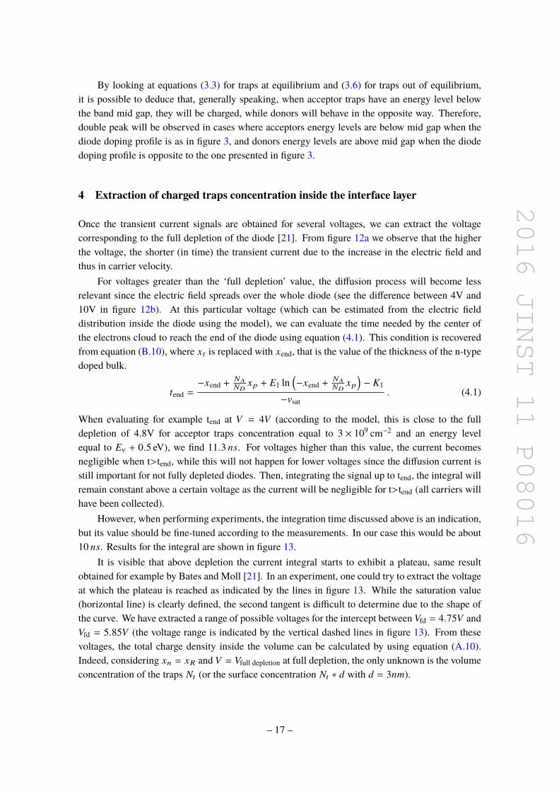
Once the transient current signals are obtained for several voltages, we can extract the voltagecorresponding to the full depletion of the diode [21]. From figure 12a we observe that the higherthe voltage, the shorter (in time) the transient current due to the increase in the electric field andthus in carrier velocity.
For voltages greater than the ‘full depletion’ value, the diffusion process will become lessrelevant since the electric field spreads over the whole diode (see the difference between 4V and10V in figure 12b). At this particular voltage (which can be estimated from the electric fielddistribution inside the diode using the model), we can evaluate the time needed by the center ofthe electrons cloud to reach the end of the diode using equation (4.1). This condition is recoveredfrom equation (B.10), where xt is replaced with xend, that is the value of the thickness of the n-typedoped bulk.
tend =−xend +
NA
NDxp + E1 ln
(−xend +
NA
NDxp
)− K1
−vsat. (4.1)
When evaluating for example tend at V = 4V (according to the model, this is close to the fulldepletion of 4.8V for acceptor traps concentration equal to 3 × 109 cm−2 and an energy levelequal to Ev + 0.5 eV), we find 11.3 ns. For voltages higher than this value, the current becomesnegligible when t>tend, while this will not happen for lower voltages since the diffusion current isstill important for not fully depleted diodes. Then, integrating the signal up to tend, the integral willremain constant above a certain voltage as the current will be negligible for t>tend (all carriers willhave been collected).
However, when performing experiments, the integration time discussed above is an indication,but its value should be fine-tuned according to the measurements. In our case this would be about10 ns. Results for the integral are shown in figure 13.
It is visible that above depletion the current integral starts to exhibit a plateau, same resultobtained for example by Bates and Moll [21]. In an experiment, one could try to extract the voltageat which the plateau is reached as indicated by the lines in figure 13. While the saturation value(horizontal line) is clearly defined, the second tangent is difficult to determine due to the shape ofthe curve. We have extracted a range of possible voltages for the intercept between Vfd = 4.75V andVfd = 5.85V (the voltage range is indicated by the vertical dashed lines in figure 13). From thesevoltages, the total charge density inside the volume can be calculated by using equation (A.10).Indeed, considering xn = xR and V = Vfull depletion at full depletion, the only unknown is the volumeconcentration of the traps Nt (or the surface concentration Nt ∗ d with d = 3nm).
– 17 –

2016 JINST 11 P08016
Figure 13. TCAD and analytical model simulations of the normalized integral of the TCT current signals atdifferent voltages. Acceptor traps level Ev + 0.5 eV , concentration 3 × 109 cm−2.
Weobtain respectively Nt ∗d = 2.78 × 109 cm−2 (forVfd = 4.75V ) and Nt ∗d=1.30 × 109 cm−2
(for Vfd = 5.85V ), while the charged traps surface concentration is 3 × 109 cm−2 (since acceptortraps with the energy level equal to Ev + 0.5 eV are fully ionized).
Therefore, using TCT data, themethod allows estimating the charged traps concentration, whilefitting the TCAD or analytical model to the obtained transient data will give a much more precisevalue for the charge stored in the interface.
5 Conclusion
In this paper, a new characterization method for bonded interfaces with deep traps is investigatedby means of numerical and analytical simulations of photo generated transient currents, the so-called TCT. It comes out that this technique is likely to be used to analyse the presence of trapsinside ultra-thin interface layers in wafer bonded monolithic detectors, and possibly in a variety ofsemiconductor heterostructures that can be fabricated with the promising low temperature waferbonding technology. This preliminary work focused on the principle of the TCT and highlightedwhat are the key technological parameters that can be assessed with this technique. In particular,the total charge density inside the device. To this purpose, we proposed a physics based modelthat helps understanding fine points of TCT for this projected application and understand whatare the most relevant physical parameters of the interface layer that can be acquired, like trapsconcentration, type and energy level. Besides, it seems that injected charges can still be collectedthrough the interface without being captured if reasonable interface trap densities and energy levelsare used and an electric field is applied.
– 18 –

2016 JINST 11 P08016
A Solution of the Poisson equation
In the following appendix, the equations for variables and constants from the solution of the Poissonequation in the cases explained in the Electrostatic modelling section, are shown, for each dioderegion.
A.1 Two space charge regions case
• Region P+, n −xL < x < −xp : in this region, silicon is not depleted, and therefore theequations will be:
◦ εP+,n (x) = 0;
◦ ΨP+,n (x) = −V .
• Region P+ −xp < x < 0: in this region, silicon is depleted, and therefore, by solving thePoisson equations:
◦ εP+ (x) = −NAqε (x + xp);
◦ ΨP+ (x) = NAq2ε
(x + xp
)2− V .
• Region 1 0 < x < xn: also in this region silicon is depleted, and therefore:
◦ ε1 (x) = NDqε x − NAq
ε xp;
◦ Ψ1 (x) = −NDq2ε x2 +
NAqε xpx + NAq
2ε x2p − V .
• Region 2 xn < x < xt −Wt
2 : Si is not depleted:
◦ ε2 (x) = 0;
◦ Ψ2 (x) = −NDq2ε x2
n +NAqε xpxn +
NAq2ε x2
p − V .
• Region t , 1 xt −Wt
2 < x < xt : Si is depleted, in this case by the charge generated by traps:
◦ εt,1 (x) = NDqε
(x − xt +
Wt
2
);
◦ Ψt,1 (x) = −NDq2ε
[x2 + x2
n +(xt −
Wt
2
)2]+
NDqε
(xt −
Wt
2
)x+ NAq
ε xpxn+NAq2ε x2
p−V .
• Region t , 2 xt < x < xt +Wt
2 :
◦ εt,2 (x) = NDqε
(x + Wt
2 − xt)−
(ND+Nt )dε q;
◦ Ψt,2(x) = −NDq2ε
(x+
Wt
2−xt
)2+
(ND+Nt )dε
q(x−xt )+NDq2ε
(Wt
2
)2
−NDq2ε
x2t+x2
n+
(xt−
Wt
2
)2+
NDqε
(xt−
Wt
2
)xt+
NAqε
xpxn+NAq2ε
x2p−V .
– 19 –

2016 JINST 11 P08016
• Region N−, xt +Wt
2 < x < xR: Silicon is not depleted:
◦ εN− (x) = 0;
◦ ΨN− (x) = −NDq2ε
W 2t +
(ND + Nt ) dε
qWt
2+
NDq2ε
(Wt
2
)2
−NDq2ε
x2t + x2
n +
(xt −
Wt
2
)2
+NDqε
(xt −
Wt
2
)xt +
NAqε
xpxn +NAq2ε
x2p − V .
To complete the set of equations, it is needed to determine the values of xp, xn and Wt .
xp =
(ND
ND + NA
)W (A.1)
xn =(
NA
ND + NA
)W (A.2)
W =
√2εq
(NA + ND
NAND
)(Vbi + V − 2kbT ) (A.3)
Wt =(ND + Nt ) d
ND. (A.4)
A.2 One space charge region case
• Region P+, n −xL < x < −xp : in this region, silicon is not depleted, and therefore theequations will be:
◦ εP+,n (x) = 0;
◦ ΨP+,n (x) = −V .
• Region P+ −xp < x < 0: in this region, silicon is depleted, and therefore, by solving thePoisson equations:
◦ εP+ (x) = −NAqε (x + xp);
◦ ΨP+ (x) = NAq2ε
(x + xp
)2− V .
• Region 1 0 < x < xt : also in this region silicon is depleted, and therefore:
◦ ε1 (x) = NDqε x − NAq
ε xp;
◦ Ψ1 (x) = −NDq2ε x2 +
NAqε xpx + NAq
2ε x2p − V .
• Region 2 xt < x < xn: Si is not depleted:
◦ ε2 (x) = NDqε x − NAq
ε xp −(ND+Nt )q
ε d;
◦ Ψ2 (x) = −NDq2ε x2 +
(NAqε xp +
(ND+Nt )qε d
)x +
{ (ND+Nt )qε dxt +
NAq2ε x2
p − V}.
• Region N−, xn < x < xR: Silicon is not depleted:
– 20 –

2016 JINST 11 P08016
◦ εN− (x) = 0;
◦ ΨN− (x) = −NDq2ε x2
n +(NAqε xp +
(ND+Nt )qε d
)xn +
{ (ND+Nt )qε dxt +
NAq2ε x2
p − V}.
To complete the set of equations, it is needed to determine the values of xp and xn.
xn=NA
NDxp+
(ND+Nt )ND
d (A.5)
xp=−(qε
NA (ND+Nt )ND
d)+
√(qε
NA (ND+Nt )ND
d)2−4 qNA
2ε
(NA
ND+1
) [ (ND+Nt )qε d
(12ND+Nt
NDd−xt
)−Vbi−V
]
qNA
ε
(NA
ND+1
) .
(A.6)
From equations (A.5) and (A.6), knowing the full depletion voltage Vfd and the length of the bulkxR, and that at full depletion xn = xR, it is possible to extract the charged traps volume density Nt .The set of equations (A.7), (A.8), (A.9) and (A.10) shows the relations that link Nt to Vfd.
aNt =
(qND
ε
)2 (1 +
NA
ND
)(A.7)
bNt =
(qND
ε
)2 (NA
ND+ 1
)xR +
q2NA
ε2 xt (NA + ND) (A.8)
cNt =
(xR
qND
ε
(NA
ND+ 1
))2− 2 (Vbi + Vfd)
qNA
ε
(NA
ND+ 1
)(A.9)
Nt = ND
*..,
bNt −
√b2Nt− aNt ∗ cNt
d ∗ aNt
− 1+//-� ND
bNt −
√b2Nt− aNt ∗ cNt
d ∗ aNt
. (A.10)
B Equations of motion of electrons
In this appendix, the solutions of the differential equation (3.11) are shown, for each region of thediode, in the one space charge region case (in the case with two space charge regions, it is possibleto consider equations until Region 1, until time tn, that is the time for which r (tn) = xn).
The notation W (x) refers to the Lambert W function of x.
• Region P+ −xp < x < 0
r = −xp + EW(
1E
evsat t+K0b
E
)+ K00a (B.1)
where:
K0,b = E ln(−K0,a
)− K0,a (B.2)
K0,a = −1 (B.3)
E =ε
µe0 NAqvsat (B.4)
– 21 –

2016 JINST 11 P08016
and ε is the silicon permittivity, µe0 is the electrons mobility at low electric field, NA isthe doping concentration of the P+ region, q is the electron charge and vsat is the saturationvelocity, given by equation
vsat = vsat,0
(300K
T
)0.87(B.5)
where vsat,0 = 1.07 × 107cm/s.
• Region 1 0 < x < xtAt time t1, the middle of the electrons cloud will reach the position 0.
t1 =xp + E ln
(K0,a−xpK0,a
)vsat
(B.6)
K1 =NA
NDxp + E1 ln
(NA
NDxp
)+ vsatt1 (B.7)
r =NA
NDxp − E1W
(1E1
e−vsat t+K1
E1
)(B.8)
whereE1 =
vsatε
NDqµe0
(B.9)
and ND is the doping concentration of the N- region. The middle of the electrons cloud willreach the position xn, in case of two separated depletion regions, at time tn.
tn =−xn +
NA
NDxp + E1 ln
(−xn +
NA
NDxp
)− K1
−vsat
since in the case of two separated depletion regions the electric fields vanishes at xn,tn = +∞.
• Region 2 xt < x < xnAt time t2, the middle of the electrons clouds will reach the position xt .
t2 =−xt +
NA
NDxp + E1 ln
(−xt +
NA
NDxp
)− K1
−vsat(B.10)
K2 = −xt +NA
NDxp +
(ND + Nt )ND
d + E1 ln(−xt +
NA
NDxp +
(ND + Nt )ND
d)+ vsatt2 (B.11)
r =NA
NDxp +
(ND + Nt )ND
d − E1W(
1E1
e−vsat t+K2
E1
). (B.12)
References
[1] N. Wermes, Pixel detectors for particle physics and imaging, applications, Nucl. Instrum. MethodsPhys. Res. Sect. A 512 (2003) 277.
[2] N. Wermes, Pixel detectors for tracking and their spin-off in imaging applications, Nucl. Instrum.Methods Phys. Res. Sect. A 541 (2005) 150.
– 22 –

2016 JINST 11 P08016
[3] L. Rossi, P. Fischer, T. Rohe and N. Wermes, Pixel Detectors. From Fundamentals to Applications,Springer-Verlag Berlin Heidelberg (2006).
[4] W. Snoeys,Monolithic pixel detectors for high energy physics, Nucl. Instrum. Methods Phys. Res.Sect. A 731 (2013) 125.
[5] C. Flötgen, N. Razek, V. Dragoi and M. Wimplinger, Novel Surface Preparation Methods forCovalent and Conductive Bonded Interfaces Fabrication, ECS Trans. 64 (2014) 103.
[6] J. Burggraf, J. Bravin, H. Wiesbauer and V. Dragoi,Monolithic thin wafer stacking using lowtemperture direct bonding, ECS Trans. 64 (2014) 95.
[7] V. Eremin, N. Strokan, E. Verbitskaya and Z. Li, Development of transient current and chargetechniques for the measurement of effective net concentration of ionized charges (Neff) in the spacecharge region of p-n junction detectors, Nucl. Instrum. Methods Phys. Res. Sect. A 372 (1996) 388.
[8] V. Eremin, E. Verbitskaya and Z. Li, The origin of double peak electric field distribution in heavilyirradiated silicon detectors, Nucl. Instrum. Methods Phys. Res. Sect. A 476 (2002) 556.
[9] G. Kramberger et al., Investigation of irradiated silicon detectors by edge-TCT, IEEE Trans. Nucl. Sci.57 (2010) 2294.
[10] M.F. García et al., High-resolution three-dimensional imaging of a depleted CMOS sensor using anedge Transient Current Technique based on the Two Photon Absorption process (TPA-eTCT), in press[Nucl. Instrum. Methods Phys. Res. Sect. (2016)].
[11] Synopsys, TCAD Sentaurus, version I–2013.12 (2013).
[12] W.R. Fahrner and S. Löffler, Determination of the Trap Density in Amorphous Silicon by Quasi-StaticCapacitance-Voltage Measurements, J. Electrochem. Soc. 145 (1998) 1786.
[13] S.M. Sze, Physics of Semiconductor Devices, John Wiley & Sons (1981).
[14] R. Eber, Investigations of new Sensor Designs and Development of an effective Radiation DamageModel for the Simulation of highly irradiated Silicon Particle Detectors, Ph.D. Thesis, KIT, KarlsruheGermany (2013), p. 150 [IEKP-KA/2013-27].
[15] J. Fink, H. Krüger, P. Lodomez and N. Wermes, Characterization of charge collection in CdTe andCZT using the transient current technique, Nucl. Instrum. Methods Phys. Res. Sect. A 560 (2006) 435.
[16] M. Moll, Radiation Damage in Silicon Detectors, Ph.D. Thesis, Universität Hamburg, HamburgGermany (1999), p. 251 and online pdf version athttps://mmoll.web.cern.ch/mmoll/thesis/pdf/moll-thesis.pdf.
[17] W. Shockley and W.T. Read, Statistics of the Recombination of Holes and Electrons, Phys. Rev. 87(1952) 835.
[18] G. Lutz, Effects of deep level defects in semiconductor detectors, Nucl. Instrum. Methods Phys. Res.Sect. A 377 (1996) 234.
[19] G. Sasso, N. Rinaldi, G. Matz and C. Jungemann, Analytical models of effective DOS, saturationvelocity and high-field mobility for SiGe HBTs numerical simulation, in International Conference onSimulation of Semiconductor Processes and Devices, IEEE (2010), p. 279.
[20] S.M. Sze, Basic equations for semiconductor-device operation, in Physics of Semiconductor Devices,2nd edition, section 1.7, Wiley (1981), pp. 50–57.
[21] A.G. Bates and M. Moll, A comparison between irradiated magnetic Czochralski and float zonesilicon detectors using the transient current technique, Nucl. Instrum. Methods Phys. Res. Sect. A 555(2005) 113.
– 23 –