· PDF file5.1 Primary 12V Power Input ... as the necessary passive components to enable PSoC...
49
Transcript of · PDF file5.1 Primary 12V Power Input ... as the necessary passive components to enable PSoC...

CONTENTS
CHAPTER 1 INTRODUCTION TO THE PME EBK...........................................................................3
1.1 Features ......................................................................................................................................................3
1.2 About the KIT.............................................................................................................................................4
1.3 PSoC Creator ..............................................................................................................................................6
1.4 Getting Help ...............................................................................................................................................6
CHAPTER 2 PME EBK ARCHITECTURE............................................................................................7
2.1 Layout and Components.............................................................................................................................7
2.2 PSoC 4+1 Power Supervisor Solution on the PME....................................................................................8
CHAPTER 3 PME EBK HARDWARE OVERVIEW.............................................................................10
3.1 2x20 pin Interface Header ........................................................................................................................ 11
3.2 PME EBK Headers and Jumpers..............................................................................................................12
3.3 Development Kit (DVK) Compatibility ...................................................................................................12
CHAPTER 4 EXAMPLE PROJECTS FOR THE PME.........................................................................13
4.1 Introduction ..............................................................................................................................................13
4.2 Software Installation.................................................................................................................................13
4.3 Hardware Setup ........................................................................................................................................14
4.4 Example Projects ......................................................................................................................................16
4.5 Power Management Component Library .................................................................................................35
4.6 Using Components in Your Own Projects ................................................................................................36
CHAPTER 5 SCHEMATICS ........................................................................................................37
5.1 Primary 12V Power Input.........................................................................................................................37
5.2 DVK Connector and Debug Test Points...................................................................................................38
5.3 Voltage Regulator V1=5V ........................................................................................................................38
5.4 Voltage Regulator V2=3.3V .....................................................................................................................39
5.5 Voltage Regulator V3=2.5V .....................................................................................................................39
1

2
5.6 Voltage Regulator V4=1.8V .....................................................................................................................39
5.7 I2C/SMBus/PMBus Interface Connector .................................................................................................40
5.8 Layout.......................................................................................................................................................40
5.8.1 Top Layer ..........................................................................................................................................40
5.8.2 Ground Layer ....................................................................................................................................41
5.8.3 Power Layer ......................................................................................................................................41
5.8.4 Bottom Layer.....................................................................................................................................42
5.8.5 Top Silkscreen ...................................................................................................................................43
5.9 Bill of Materials........................................................................................................................................44
CHAPTER 6 APPENDIX.....................................................................................................................48
6.1 Revision History.......................................................................................................................................48
6.2 Copyright Statement .................................................................................................................................48

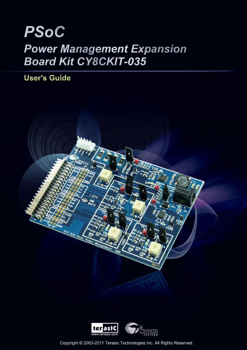
Chapter 1 Introduction to the PME EBK
In general terms, power management or power supervision is a combination of sequencing, monitoring and control of multiple regulators and/or point-of-load DC power converters in a system. Typical solutions for power management include multiple devices such as CPLDs, mixed-signal ASICs and/or limited-functionality and inflexible discrete devices. Power management solutions require: (1) rapid fault detection capabilities for high-availability systems of the power converters in the system; (2) accurate and reliable power rail sequencing of the power converters during power-on and power-off events; (3) voltage and current measurement of the power converters to optimize power consumption and/or for data logging; and, (4) closed-loop control of the power converters through trimming and, for development and manufacturing test purposes, margining of voltage rails in the system. The PSoC Power Management Expansion Board Kit (PME EBK) is part of the PSoC development kit ecosystem and is designed to work with the CY8CKIT-001 PSoC Development Kit (DVK) and the CY8CKIT-030 PSoC 3 Development Kit (DVK). It enables you to evaluate the system power management functions and capabilities of PSoC 3 devices. You can evaluate the example projects described in this guide or design and customize your own system power management solution using components in Cypress's PSoC CreatorTM software (included in this kit) or by altering example projects provided with this kit. The PSoC Power Management Expansion Board Kit (PME EBK) is used with the PSoC family of devices and is specifically designed and packaged for use with the PSoC 3 device family. PSoC 3 is a programmable system-on-chip platform that combines precision analog and digital logic with a high performance, single-cycle, 67MHz 8051 processor. With the flexibility of the PSoC architecture, you can easily create your own custom power management solution on chip with the exact functionality you need, in the way you want it—no more, no less.
1.1 Features
The PSoC Power Management Expansion Board Kit (PME EBK) is intended to provide a demonstration and development platform for Cypress and customers in developing power management/supervisor solutions including: • Power Supply Sequencing • Power Supply Voltage and Current Measurement • Power Supply Voltage Trimming and Margining • Power Supply Over-Voltage and Under-Voltage Fault Detection • EEPROM Data Recording • I2C/SMBus/PMBus Host Communications Interface
3

Figure 1-1 shows a simplified block diagram of the most fundamental components on the PME EBK and how they interact to aid in understanding of the hardware. Not all hardware components are shown.
Figure 1-1 PME EBK Block Diagram
1.2 About the KIT
The PSoC Power Management Expansion board kit (PME) consists of: • Cypress PME EBK • Quick Start Guide • Power DC Adaptor 12V/2A • System CD containing:
User’s Guide (this document) PSoC Creator and pre-requisite software PSoC Programmer and pre-requisite software PME Example Firmware for the CY8CKIT-001 PSoC Development Kit
Advanced Sequencer Power Supervisor
4

PME Example Firmware for the CY8CKIT-030 PSoC 3 Development Kit Advanced Sequencer Power Supervisor
Application Note (AN62496) “Voltage Sequencing with PSoC ® 3 and PSoC ® 5” Application Note (AN60220) “Multiplexed Comparator using PSoC ® 3” Datasheets for key PME EBK components
Figure 1-2 shows a photograph of the PME EBK contents.
Figure 1-2 PME EBK Package Contents
5

6
1.3 PSoC Creator
Cypress's PSoC Creator software is a state-of-the-art, easy-to-use integrated development environment (IDE) that introduces a game changing, hardware and software design environment based on classic schematic entry and revolutionary embedded design methodology.
With PSoC Creator, you can:
• Draw a schematic of the hardware circuit you would like to build inside PSoC and the tool will automatically place and route the components for you
• Eliminate external CPLDs or standard logic ICs by integrating state machines and simple glue logic in your design Trade-off architecture decisions between hardware and software, allowing you to focus on what matters and getting you to market faster
PSoC Creator also enables you to tap into an entire tools ecosystem with integrated compiler tool chains, RTOS solutions, and production programmers to support PSoC 3.
1.4 Getting Help
Certified as a Cypress Authorized Design Partner, Terasic offers design expertise in rapidly developing PSoC Solutions to get your products into production quickly and reducing your development and BOM costs. Terasic provides customized board designs for academia and industry.
For additional information visit:
www.cypress.com/go/CY8CKIT-035 or http://pme.terasic.com
For support please contact:
Online: www.cypress.com/go/support Telephone (24x7): +1-800-541-4736 ext. 8 (USA) +1-408-943-2600 ext. 8 (International)

Chapter 2 PME EBK Architecture
This chapter provides information about the architecture and block diagram of the PME EBK.
2.1 Layout and Components
Photos of the PME EBK are shown in Figure 2-1 and Figure 2-2. They depict the layout of the board and indicate the locations of the connectors and key components.
Figure 2-1 PME PCB (Top)
7
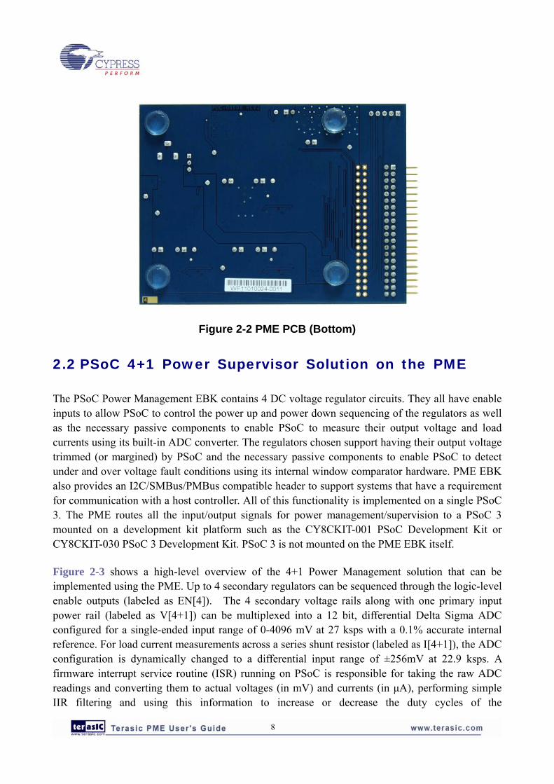
Figure 2-2 PME PCB (Bottom)
2.2 PSoC 4+1 Power Supervisor Solution on the PME
The PSoC Power Management EBK contains 4 DC voltage regulator circuits. They all have enable inputs to allow PSoC to control the power up and power down sequencing of the regulators as well as the necessary passive components to enable PSoC to measure their output voltage and load currents using its built-in ADC converter. The regulators chosen support having their output voltage trimmed (or margined) by PSoC and the necessary passive components to enable PSoC to detect under and over voltage fault conditions using its internal window comparator hardware. PME EBK also provides an I2C/SMBus/PMBus compatible header to support systems that have a requirement for communication with a host controller. All of this functionality is implemented on a single PSoC 3. The PME routes all the input/output signals for power management/supervision to a PSoC 3 mounted on a development kit platform such as the CY8CKIT-001 PSoC Development Kit or CY8CKIT-030 PSoC 3 Development Kit. PSoC 3 is not mounted on the PME EBK itself.
Figure 2-3 shows a high-level overview of the 4+1 Power Management solution that can be implemented using the PME. Up to 4 secondary regulators can be sequenced through the logic-level enable outputs (labeled as EN[4]). The 4 secondary voltage rails along with one primary input power rail (labeled as V[4+1]) can be multiplexed into a 12 bit, differential Delta Sigma ADC configured for a single-ended input range of 0-4096 mV at 27 ksps with a 0.1% accurate internal reference. For load current measurements across a series shunt resistor (labeled as I[4+1]), the ADC configuration is dynamically changed to a differential input range of ±256mV at 22.9 ksps. A firmware interrupt service routine (ISR) running on PSoC is responsible for taking the raw ADC readings and converting them to actual voltages (in mV) and currents (in μA), performing simple IIR filtering and using this information to increase or decrease the duty cycles of the
8

pulse-width-modulated (PWM) outputs for regulator trimming and margining. The trim/margin PWM outputs from PSoC (labeled as TR[4]) are filtered with a single RC filter stage on PME EBK and fed into the voltage feedback input of the regulators. A single time-multiplexed window comparator is implemented in PSoC using 2 voltage DAC’s (to set the under and over voltage limits for each rail), 2 comparators and a programmable glitch filter. This window comparator loops through each channel at 2μs per channel that it monitors (labeled as C[4+1]). Note that all 5 monitored supply rail voltages are connected to both the V[4+1] and C[4+1] input pins. Each voltage is connected to 2 pins to enable the hardware window comparator and the ADC with input multiplexer to run asynchronously to each other at different speeds in order to give the fastest possible fault detection time.
Figure 2-3 4+1 PSoC Power Management Functional Diagram
Note that PME EBK hardware limits support to a maximum of 4 secondary regulator circuits. The PSoC 3 Power Supervisor solution can be easily extended to support up to 12 secondary regulator circuits. Contact Cypress for further information on the full 12+1 PSoC Power Supervisor solution.
9

Chapter 3 PME EBK Hardware Overview
Figure 3-1 PME Hardware Components
The Power Management EBK Board consists of a 12V primary input power source and 4 secondary voltage rails: V1=5V, V2=3.3V, V3=2.5V and V4=1.8V. Voltage rail V1 feeds power to the other three rails V2, V3 and V4. Therefore, disabling V1 will disable V2-V4 as a result. Each secondary rail consists of a regulator with enable input, circuitry that enables PSoC to apply a DC control voltage to the regulator feedback or adjust pin, as well as fixed and adjustable (potentiometer) load elements. Two jumpers are provided for each rail to (1) disconnect all loads or (2) disconnect only the adjustable load. PME EBK provides an I2C/SMBus/PMBus connector. A 40-pin (2×20) header J1 is provided to interface this board with the host PSoC on a development kit platform such as the CY8CKIT-001
10

11
PSoC Development Kit or CY8CKIT-030 PSoC 3 Development Kit. The header carries voltage enables, regulator voltage, regulator load currents and trim/margin control signals for each regulator on PME EBK. The I2C physical layer signals (SDA/SCL) from PSoC are also routed across this header to enable connection to an external host or management processor that supports standard I2C, SMBus or PMBus protocol interfaces.
3.1 2x20 pin Interface Header
The following table outlines the definition of the 40-pin J1 header interface.
Table 3-1 2x20 Header (J1) Pin Definition Description Signal Pin Pin Signal Description Voltage Regulator 4, Enable V4EN 1 2 V3EN Voltage Regulator 3, Enable Voltage Regulator 2, Enable V2EN 3 4 V1EN Voltage Regulator 1, Enable - NC 5 6 NC - Power Rail Current (measured as single ended voltage)
IIN 7 8 VIN Power Rail Sensing Voltage
Analog Ground AGND 9 10 NC - Voltage Regulator 4, Fault Sensing Voltage
C4 11 12 C3 Voltage Regulator 3, Fault Sensing Voltage
Voltage Regulator 2, Fault Sensing Voltage
C2 13 14 C1 Voltage Regulator 1, Fault Sensing Voltage
Voltage Regulator 4, Trim TR4 15 16 TR3 Voltage Regulator 3, Trim Voltage Regulator 2, Trim TR2 17 18 TR1 Voltage Regulator 1, Trim Analog Ground AGND 19 20 NC - Voltage Regulator 4, Current (Measured as differential voltage)
I4 21 22 V4 Voltage Regulator 4
Voltage Regulator 3, Current (Measured as differential voltage)
I3 23 24 V3 Voltage Regulator 3
Voltage Regulator 2, Current (Measured as differential voltage)
I2 25 26 V2 Voltage Regulator 2
Voltage Regulator 1 Current (Measured as single ended voltage)
I1 27 28 V1 Voltage Regulator 1
Analog Ground AGND 29 30 NC - - NC 31 32 /ALERT Alert Signal (I2C/SMBus/PMBus) Serial Data (I2C/SMBus/PMBus) SDAT 33 34 SCL Serial Clock (I2C/SMBus/PMBus)unused D3V3 35 36 VADJ unused Digital Ground DGND 37 38 D5V unused Optional 12V Power from DVK DVIN 39 40 DGND Digital Ground

12
3.2 PME EBK Headers and Jumpers
A number of headers and jumpers are provided on the PME EBK. The following table outlines the function of each item and the default configuration.
Table 3-2 PME Jumper Settings PCB Designator
Description Factory Default Configuration
J1 2×20 pin header for connecting to PSoC DVK - J2 5-pin header for connecting an external host or management
processor via I2C/SMBus/PMBus -
J3 Power Jack - J4 2×20 pin header that replicates signals on J1 for easy connection to a
logic analyzer or oscilloscope -
J5 3-pin header for primary input power source selection. Place jumper in 1-2 position to source power from the DC power jack J3. Place in 2-3 position to source power from the PSoC platform DVK
2-3 position
J6 2-pin header for connecting all loads on V1=5V rail (this includes the fixed and adjustable loads on V1 as well as the load presented by the V2, V3 and V4 rails)
Installed
J7 2-pin header for connecting the potentiometer load on V1=5V rail Installed J8 2-pin header for connecting both loads on V2=3.3V rail (fixed and
adjustable) Installed
J9 2-pin header for connecting potentiometer load on V2=3.3V rail Installed J10 2-pin header for connecting ALL loads on V3=2.5V rail (fixed and
adjustable) Installed
J11 2-pin header for connecting variable potentiometer on V3=2.5V rail Installed J12 2-pin header for connecting ALL loads on V4=1.8V rail (fixed and
adjustable) Installed
J13 2-pin header for connecting variable potentiometer on V4=1.8V rail Installed
3.3 Development Kit (DVK) Compatibility
This kit contains an expansion board only and requires a Cypress development kit platform in order to use it. This kit is compatible with both the CY8CKIT-001 PSoC DVK and the CY8CKIT-030 PSoC 3 DVK. NOTE: Early revisions of the CY8CKIT-001 PSoC Development Kit contained an early engineering sample release (ES2) of the PSoC 3 CY8C38xxx Device Family Processor Module which is not compatible with the example projects that accompany this kit. If you have an early revision of the kit you can upgrade free of charge at www.cypress.com/go/psoc3kitupgrade.

Chapter 4 Example Projects for the PME
4.1 Introduction
This section provides details on how to operate the hardware and run the example projects provided.
4.2 Software Installation
Perform the following steps to install the PSoC PME EBK software: Insert the kit CD into the CD drive of your PC. The CD is designed to auto-run and the kit menu should appear. (See Figure 4-1)
Figure 4-1 CD Autorun Kit Menu
NOTE: If auto-run does not execute, double-click AutoRun on the root directory of the CD. After the installation is complete, the kit contents are available at the following location: C:\Program Files\Terasic\PSoC Power Management EBK\1.0
13

When installing the PSoC Power Management EBK software, the installer checks if your system has the required software. This includes PSoC Creator, PSoC Programmer, Windows Installer, .NET framework, Adobe Acrobat Reader, and KEIL Compiler. If these applications are not installed, then the installer prompts you to install all pre-requisite software, which is also available on the kit CD. The software can be uninstalled using one of the following methods:
Go to Start > Control Panel > Add or Remove Programs; select appropriate software package; select the Remove button.
Go to Start > All Programs > Cypress > Cypress Update Manager > Cypress Update Manager; select the Uninstall button for the appropriate software package.
Insert the kit CD and click Install the kit contents from CD button. In the CyInstaller for PSoC Power Management EBK 1.0 window, select Remove from the Installation Type drop-down menu. Follow the instructions to uninstall. (NOTE: this method will only un install the kit software and not all the other material/software that may have been installed along with the kit software)
4.3 Hardware Setup
The kit includes example projects for both the CY8CKIT-001 PSoC DVK and the CY8CKIT-030 PSoC 3 DVK hardware platforms. The main difference between the projects for the two hardware platforms is the PSoC pin mapping. Other differences will be highlighted in the sections that describe details of the example projects. The following sections describe how to set up the hardware to run the example projects. For a given DVK base platform, the same hardware configuration applies to both example projects.
CY8CKIT-001 PSoC DVK
1. Using the pin header/breadboard area of the PSoC DVK base board, use jumper wires to make the following connections:
“SW1” to P1_4 “SW2” to P1_5
Figure 4-2 CY8CKIT-001 PSoC DVK Breadboard
14

2. Set the system to run at 5V using SW3 and set J6 “VDD DIG” and J7 “VDD ANLG” to VDD=5V using J6 and J7 as shown below:
Figure 4-3 CY8CKIT-001 PSoC DVK Power Jumpers
3. Ensure that the LCD character display included with PSoC DVK is attached and that the LCD power jumper (J12) is in the ON position:
Figure 4-4 CY8CKIT-001 PSoC DVK LCD Power Jumper
CAUTION: Do not attach the PSoC Power Management EBK to the PSoC DVK until you have programmed the PSoC with one of the example projects. The GPIOs routed to the PSoC Power Management EBK connect to the power regulator circuits which may be damaged if firmware previously programmed into PSoC drives those pins. Once the PSoC has been programmed, attach the PSoC Power Management EBK to PORT A of the PSoC DVK.
15
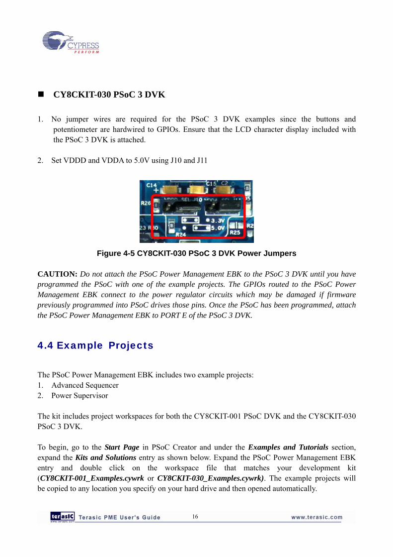
CY8CKIT-030 PSoC 3 DVK
1. No jumper wires are required for the PSoC 3 DVK examples since the buttons and potentiometer are hardwired to GPIOs. Ensure that the LCD character display included with the PSoC 3 DVK is attached.
2. Set VDDD and VDDA to 5.0V using J10 and J11
Figure 4-5 CY8CKIT-030 PSoC 3 DVK Power Jumpers
CAUTION: Do not attach the PSoC Power Management EBK to the PSoC 3 DVK until you have programmed the PSoC with one of the example projects. The GPIOs routed to the PSoC Power Management EBK connect to the power regulator circuits which may be damaged if firmware previously programmed into PSoC drives those pins. Once the PSoC has been programmed, attach the PSoC Power Management EBK to PORT E of the PSoC 3 DVK.
4.4 Example Projects
The PSoC Power Management EBK includes two example projects: 1. Advanced Sequencer 2. Power Supervisor The kit includes project workspaces for both the CY8CKIT-001 PSoC DVK and the CY8CKIT-030 PSoC 3 DVK. To begin, go to the Start Page in PSoC Creator and under the Examples and Tutorials section, expand the Kits and Solutions entry as shown below. Expand the PSoC Power Management EBK entry and double click on the workspace file that matches your development kit (CY8CKIT-001_Examples.cywrk or CY8CKIT-030_Examples.cywrk). The example projects will be copied to any location you specify on your hard drive and then opened automatically.
16

Figure 4-6 PSoC Creator Start Page showing Kits and Solutions
The example projects will be displayed in the Workspace Explorer window as shown in the example below for the CY8CKIT-001 PSoC DVK:
Figure 4-7 Workspace Explorer View
Running the Example Firmware: CY8CKIT-001 PSoC DVK
Make sure the hardware has been configured according to the Hardware Setup section. 1. If this is the first time that the example project firmware is being programmed into PSoC, make
sure the PSoC Power Management EBK is not connected to the PSoC DVK 2. Apply 12 VDC power to the PSoC DVK 3. Attach the MiniProg3 first to a USB port on the PC and then to the PROG port on the
17

CY8CKIT-009 PSoC 3 Processor Module 4. In PSoC Creator, set the appropriate example project as active by right clicking on it in the
Workspace Explorer and selecting Set As Active Project 5. In PSoC Creator, select Debug > Program to program PSoC 6. Remove power from the PSoC DVK and attach the PSoC Power Management EBK to Port A
of the PSoC DVK 7. On the PSoC Power Management EBK board, make sure the power jumper (J5) is set to
“DVK” (the default setting) 8. Apply 12 VDC power to the PSoC DVK 9. If the PME EBK cannot be detected by PSoC, status debug messages will be displayed on the
LCD to assist with rectifying the problem
Figure 4-8 CY8CKIT-001 PSoC DVK with PSoC Power Management EBK
Connected to Port A (Running Example 2)
Running the Example Firmware: CY8CKIT-030 PSoC 3 DVK
Make sure the hardware has been configured according to the Hardware Setup section. 1. If this is the first time that the example project firmware is being programmed into PSoC, make
sure the PSoC Power Management EBK is not connected to the PSoC 3 DVK 2. Attach a USB cable from the PC to the PSoC 3 DVK Program/Debug USB port (use J1 - the
USB connector closest to the corner of the board) 3. In PSoC Creator, set the appropriate example project as active by right clicking on it in the
Workspace Explorer and selecting Set As Active Project 4. In PSoC Creator, select Debug > Program to program PSoC 5. Remove the USB cable from the PSoC 3 DVK and attach the PSoC Power Management EBK
to Port E of the PSoC 3 DVK
18

6. On the PSoC Power Management EBK board, make sure the power jumper (J5) is set to “EXT”. Note that this is not the default setting for the J5 jumper.
7. Apply 12 VDC power to the PSoC Power Management EBK using J3 8. Re-attach the USB cable from the PC to the PSoC 3 DVK Program/Debug USB port (use J1 -
the USB connector closest to the corner of the board) 9. If the PME EBK cannot be detected by PSoC, status debug messages will be displayed on the
LCD to assist with rectifying the problem 10. Going forward, every time PSoC is re-programmed, press the Reset (SW1) button on the PSoC
3 DVK to run the newly programmed firmware image
Figure 4-9 CY8CKIT-030 PSoC 3 DVK with PSoC Power Management EBK Connected
to Port E (Running Example 2)
19

Example 1: Advanced Sequencer
Overview
This example demonstrates the following features: 1. Voltage sequencing 2. Under-voltage/over-voltage monitoring using the window comparator for rapid fault detection If the project is running correctly, all 4 green LEDs on the PSoC Power Management EBK should be turned on and the debug LCD should display something like this: (See Figure 4-10)
Figure 4-10 Example1 - LCD Display for Normal Operation
The 4 digits indicate the rail failure status (under-voltage=UV or over-voltage=OV). A dash ‘-’ indicates that the rail is within defined operating limits (+/- 7.5% of nominal voltage). If a failure occurs on any rail, the rail number will be displayed next to the UV or OV indicator. For example, if you remove jumper J6, then you will remove power to regulators 2 through 4. This should cause an under-voltage (UV) fault on rails 2 through 4. In that case, the display should look like this: (see Figure 4-11)
Figure 4-11 Example1 - LCD Display when J6 Removed
Note also that the Voltage Sequencer component has been configured to shut down all rails on any fault condition, so all 4 green LEDs on PME EBK should turn off when jumper J6 is removed. Changing this default behavior will be described in the next section. To power up the sequencer again, replace J6 and then press and hold the retry switch (SW2 on the CY8CKIT-001 PSoC DVK and SW3 on the CY8CKIT-030 PSoC 3 DVK).
20

Technical Details – Voltage Sequencing
This example builds upon the Voltage Sequencer component discussed in Cypress Application Note AN62496 “Voltage Sequencing with PSoC® 3 and PSoC® 5”. The Voltage Sequencer component enables designers to control both the power-up and power-down sequence and timing of up to 16 secondary-side voltage supplies. It is designed to interface to regulators that provide a digital power good (PGOOD) status output. In this example project, the regulators on the PSoC Power Management EBK are monitored using the under-voltage/over-voltage window comparator logic inside PSoC with programmable thresholds on each rail which generate equivalent PGOOD signals internally that connect to the Voltage Sequencer component. (See Figure 4-12)
Figure 4-12 Advanced Sequencer Architecture
To change the behavior of the sequencer, double click on the Voltage Sequencer in the Example1 top-level design schematic file. (See Figure 4-13)
Figure 4-13 Voltage Sequencer Component
This will open the component customizer for the Voltage Sequencer. The General Tab will be presented first by default. (See Figure 4-14)
21

Figure 4-14 Voltage Sequencer Customizer General Tab
For this example project, the key parameter settings are the number of rails (4), Auto Power Up and Auto Power Down settings and Rail Fail interrupts. Those settings enable the component to automatically sequence the regulators up and down with minimal firmware. Refer to AN62496 for full details of the configuration options presented here. Click on the Rails Tab to setup the voltage regulator controls, primarily used in this example project to set the polarity of the regulator enable signals to active high for compatibility with the regulators installed on the PSoC Power Management EBK. (See Figure 4-15)
Figure 4-15 Voltage Sequencer Customizer Rails Tab
Click on the Sequencer Tab to configure the sequencing options. In this example project, each rail is assigned its own sequencing time slot. The matrix of checkboxes currently shows that timing slot
22

1 is associated with regulator 1. Timing slot 2 with regulator 2 etc. Changing the checkbox assignments will change the sequence of powering up the regulators on PME EBK. Since rails 2 through 4 derive their input power from the output of regulator 1 (this is a hardwired connection on PME EBK), we will always need to power up rail 1 first. Therefore, the checkbox assigning rail 1 to slot 1 will always need to be assigned that way when working with the PME EBK. Feel free to re-configure the power-up sequence of the other 3 rails (V2 through V4). The timing of the power-up sequence is controlled by the Ramp and Up Delay parameters both expressed in units of 1 ms (NOTE: this unit is customizable. Refer to Cypress application note AN62496 for more details). The Ramp parameter defines how long the Voltage Sequencer should wait after enabling a regulator before checking for pass or fail on the PGOOD input. The Up Delay parameter defines how long the Voltage Sequencer should wait once the timing slot has powered-up successfully before moving on to the next timing slot. This provides external components powered by the regulator the time needed to power up and initialize properly before moving to the next power/timing slot. (See Figure 4-16 below for the correct configuration).
Figure 4-16 Voltage Sequencer Customizer Sequencer Tab
The Power Down pull-down menu control specifies how the regulators should be turned off in case of fault or system power down. The All Off setting sets it to simultaneous shutdown. Forward and Reverse are 2 other built-in options that enable designers to control the power-down sequence and timing (controlled by the Dn Delay parameter). The chart in the upper part of this tab displays the current sequencer configuration for visual confirmation that the settings have been entered correctly.
23
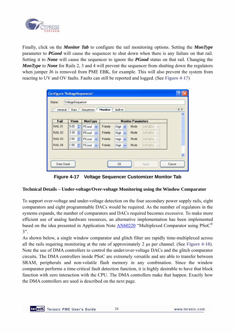
Finally, click on the Monitor Tab to configure the rail monitoring options. Setting the MonType parameter to PGood will cause the sequencer to shut down when there is any failure on that rail. Setting it to None will cause the sequencer to ignore the PGood status on that rail. Changing the MonType to None for Rails 2, 3 and 4 will prevent the sequencer from shutting down the regulators when jumper J6 is removed from PME EBK, for example. This will also prevent the system from reacting to UV and OV faults. Faults can still be reported and logged. (See Figure 4-17)
Figure 4-17 Voltage Sequencer Customizer Monitor Tab
Technical Details – Under-voltage/Over-voltage Monitoring using the Window Comparator
To support over-voltage and under-voltage detection on the four secondary power supply rails, eight comparators and eight programmable DACs would be required. As the number of regulators in the systems expands, the number of comparators and DACs required becomes excessive. To make more efficient use of analog hardware resources, an alternative implementation has been implemented based on the idea presented in Application Note AN60220 “Multiplexed Comparator using PSoC® 3”. As shown below, a single window comparator and glitch filter are rapidly time-multiplexed across all the rails requiring monitoring at the rate of approximately 2 μs per channel. (See Figure 4-18). Note the use of DMA controllers to control the under/over-voltage DACs and the glitch comparator circuits. The DMA controllers inside PSoC are extremely versatile and are able to transfer between SRAM, peripherals and non-volatile flash memory in any combination. Since the window comparator performs a time-critical fault detection function, it is highly desirable to have that block function with zero interaction with the CPU. The DMA controllers make that happen. Exactly how the DMA controllers are used is described on the next page.
24

Figure 4-18 Time Multiplexed Over/Under Voltage Detection Hardware
The time-multiplexing works according to this sequence: 1. The scaled regulator output for rail[n] (signal C[n]) is multiplexed into the window comparator 2. The under and over voltage limits for rail[n] are copied from SRAM to the DAC using DMA 3. The previous glitch filter result for rail[n] is copied from SRAM to the glitch filter using DMA 4. A short delay is provided to allow the DACs and comparators time to settle and stabilize 5. The comparator over/under voltage results are sampled by the glitch filters 6. The current glitch filter result for rail[n] is copied back to SRAM using DMA 7. Connection to rail[n] (signal C[n]) is removed 8. The next rail[n+1] (signal C[n+1]) is selected and steps 1 to 7 repeat for that rail Note that on the PSoC Power Management EBK, the four secondary regulator output voltages (signals C[4:1]) are all normalized to about 1 volt using scaling resistors in order to use the internal DAC’s fastest update rate of 1,000 ksps using the 1 volt range (the DAC’s 4V range update rate is 250 ksps). Scaling the input voltage gives the best possible performance. If higher speed is not required for your application, and all the secondary rails in your system are lower than 4 V (the maximum DAC range), scaling of the regulator outputs can be eliminated.
Technical Details – Firmware Flowchart
The window comparator fault detection circuit is entirely hardware driven after it is initialized. That frees the 8051 CPU core 100% to do other application-specific user tasks. In the Example1 project, the user task is updating the LCD display and handling switch presses. The Voltage Sequencer component is primarily firmware driven, and since it is a critical system-level function, it consumes the 8051 CPU core 100% through blocking application programmer interface (API) calls when in use. The Voltage Sequencer component firmware only runs in 2 cases: 1) when the system is powered up at which time the selected power-up sequence is executed. This includes the sequence in which the regulators are enabled, and execution of the timing delays specified by the Ramp and Up Delays entered into the component customizer and 2) when the system is powered down due to a regulator fault, as detected by the window comparator hardware. When all regulators are powered on and running, the Voltage Sequencer component uses
25

digital logic to constantly monitor the selected PGOOD inputs to make sure they are good. Any failure on any selected PGOOD input will cause an interrupt to the CPU core which will then call the Voltage Sequencer component power down API until the system is safely turned off. The firmware flowchart for the Example1 project is shown below (See Figure 4-19)
Display LCDIntro Message
Start Window ComparatorH/W Block
Check for EBKConnection
Start Voltage Sequencer Component
Enable Regulator n
Execute RampDelay for Slot n
PGOOD[n]OK?
Execute Up Delay for Slot [n]
n=n+1
n <= 4?
Handle User Interface
DisableAll Regulators
PGOODFailure Interrupt
Resetor Power On
n=1
Y
N
Y
N
Figure 4-19 Example1 Firmware Flowchart
26

Example 2: 4+1 Power Supervisor
Overview
This example builds on the Example1 project and demonstrates a much more comprehensive power supervisor solution with the following features: 3. Power supply sequencing 4. Power supply voltage and current measurement accurate to better than 1% 5. Power supply trimming and margining accurate to better than 1% 6. Power supply over-voltage and under voltage fault detection using window comparators 7. EEPROM storage for fault logging, calibration parameters and general purpose storage 8. I2C host communication interface
If the project is running correctly, all 4 green LEDs on the PSoC Power Management EBK should be turned on and the debug LCD should display something like that shown below. (See Figure 4-20)
Figure 4-20 LCD Display - Voltages
The 1mV display in the top left corner indicates the units of the 4+1 power supply voltage measurements. The next 2 numbers on the 1st line of the display indicate the measured 12 V primary input voltage value and the measured 5 V rail value. The 2nd line of the display indicates the measured 3.3 V, 2.5 V and 1.8 V rail values. Note that regulator trimming is being performed by PSoC automatically to regulate the 4 secondary voltages to better than 1% accuracy of nominal output. The primary 12 V input supply cannot be controlled by PSoC so the nominal voltage displayed will probably not be within 1% of nominal. Pressing and releasing SW1 on the CY8CKIT-001 PSoC DVK (SW2 on the CY8CKIT-030 PSoC 3 DVK) will display the supply currents measured on the Power Management EBK by PSoC. (See Figure 4-21)
27

Figure 4-21 LCD Display - Currents
The 0.1mA reading in the top left corner indicates the units of the 4+1 power supply current measurements. The next 2 numbers on the 1st line of the display indicate the measured 12 V primary input load current value and the measured 5 V rail load current value. The 2nd line of the display indicates the measured 3.3 V, 2.5 V and 1.8 V rail load current values. Loads can be adjusted on PME EBK using the potentiometers. The load currents measured by PSoC’s ADC converter can be compared with a digital multimeter (DMM) by removing the appropriate jumper and connecting the DMM configured to measure current. When currents are displayed on the LCD, pressing and holding the SW1 on the CY8CKIT-001 PSoC DVK (SW2 on the CY8CKIT-030 PSoC 3 DVK) for a longer period will enable manual trimming control. The example below shows the manual trimming display for rail 1 (+5V nominal). (See Figure 4-22)
Figure 4-22 LCD Display - Trimming
The top line of the display shows the actual voltage of the rail currently measured by PSoC. The left side of the second line shows the deviation from the nominal 5V as a percentage. The right side of the second line shows the current PWM duty cycle used by the trimming hardware to achieve the currently selected voltage. In this mode, pressing and releasing SW1 on the CY8CKIT-001 PSoC DVK (SW2 on the CY8CKIT-030 PSoC 3 DVK) will trim the rail down in steps of approximately 2%. Pressing and releasing the SW2 on the CY8CKIT-001 PSoC DVK (SW3 on the CY8CKIT-030 PSoC 3 DVK) will trim the rail up in steps of approximately 2%. The actual voltages and PWM duty cycles will update in response to switch presses. Trimming below or above the nominal voltage by more than 7.5% will cause the under/over voltage window comparator fault detection circuit to trip which will cause all regulators to be turned off by the Voltage Sequencer component. The green LEDs on the Power Management EBK will all be turned off in that case and the LCD will report that a “Rail Failure” has occurred. To re-start the voltage sequencer, press and hold SW2 on the CY8CKIT-001 PSoC DVK (SW3 on the CY8CKIT-030 PSoC 3 DVK) until the regulators power up again, indicated by the green LEDs on PME EBK turning on in sequence.
28

29
When the trimming menu is displayed, pressing and holding SW1 on the CY8CKIT-001 PSoC DVK (SW2 on the CY8CKIT-030 PSoC 3 DVK) for a longer period will enable manual trimming control for the next secondary regulator. To get back to the main voltage display menu, cycle through all 4 manual trim menus by pressing and holding SW1 on the CY8CKIT-001 PSoC DVK (SW2 on the CY8CKIT-030 PSoC 3 DVK) for a longer period.
Technical Details – Voltage Sequencer and Under/Over-Voltage Fault Detection
The voltage sequencer and under/over-voltage window comparator circuits are fundamentally the same in this example as they were for Example1, so they will not be discussed again here. One thing to note is that when running the example project on the CY8CKIT-030 PSoC 3 DVK, only 2 of the voltage rails (V1=5V and V3=2.5V) can be routed to the window comparator circuit due to the PSoC port pins available on Port E of the DVK. The other voltage rails (V2=3.3V and V4=1.8V) are monitored using the ADC and compared against the under/over voltage thresholds using a +/-10% window. When running this example project on the CY8CKIT-030 PSoC 3 DVK, it may not be possible to generate faults on those rails using the switches in the trimming menus.
Technical Details – Voltage and Current Measurements
In Example2, voltage rail voltage and current measurements use the differential 12-bit Delta-Sigma ADC with 0.1% internal accurate voltage reference. The PSoC Creator circuit is shown below: (Figure 4-23)

Figure 4-23 ADC Converter Schematic
For measuring voltages, the Delta-Sigma ADC is configured to use a ±2048 mV input range with a 2048 mV reference (generated by doubling the internal 1024 mV reference) on the negative input terminal, yielding an actual single-ended voltage measurement range of 0 to 4096 mV. This range is used to measure the voltages of each of the regulator rails on the PSoC Power Management EBK. For the V2=3.3 V, V3=2.5 V and V4=1.8 V rails, those voltages are compatible with the ADC setting and can be directly connected to PSoC (V2, V3 and V4 in the schematic shown above). For the V1=5 V and the primary 12 V input, the voltages are scaled using external resistors to make them compatible with the ADC input voltage range at the expense of some additional measurement inaccuracy caused by the tolerances of the external resistors used (VIN and V1 in the schematic shown above). Two different methods are used for current measurement, also depending on the voltage being measured. For the V2=3.3 V, V3=2.5 V and V4=1.8 V rails, a high-side shunt resistor is placed in series with the regulator output. The differential voltage developed across that resistor is directly proportional to load current. To support that measurement, the ADC configuration is dynamically changed to a ± 256 mV range. To minimize voltage loss and power dissipation, the resistance value is chosen to be as low as possible and should be 0.1% tolerance in order to maintain overall system measurement accuracy of < 1%. For the V1=5 V and the primary 12 V input, the current shunt resistor method cannot be used directly. Attempting to scale both sides of the current shunt resistor to a lower voltage range adds error to the measurement that is difficult to calibrate out. For those rails, the PSoC Power Management EBK uses low cost external current sense amplifiers (such as the Zetex ZXCT1009 or Maxim 4080), that detect the differential voltage across the shunt resistor and convert it to a single-ended voltage compatible with the ADC input voltage range. ADC conversion time depends on several factors including the CPU clock frequency inside PSoC,
30

31
the resolution of the ADC and the time taken to switch inputs and change ADC configuration. At a CPU clock frequency of 24MHz (as used in Example2), the time taken to execute those fundamental tasks is outlined below:
1. Using the ±2048 mV range: 65 μs per reading 2. Changing to ±256mV range: 320 μs 3. Using the ±256 mV range: 83 μs per reading 4. Changing to ±2048 mV range: 320 μs
For example, to measure the voltage and the current of the 4+1 rails on the PSoC Power Management EBK would take: (see Table 4-1)
Table 4-1 ADC Conversion Time Function Time 5 single ended voltages on the ±2048 mV range (VIN, V1-V4)
5* 65 μs
2 single ended current measurements using the external current sense amps (IIN, I1)
2* 65 μs
Switch ADC to differential mode 1* 320 μs 3 differential current measurements across shunt resistors (I2-I4)
3* 83 μs
Switch ADC to single ended mode 1* 320 μs Total 1344 μs or approximately 270 μs average per rail
Technical Details – Regulator Trimming and Margining
Trimming (fine tuning) of each regulator output is achieved by applying a controlled analog voltage to the “feedback” (VFB) or “adjust” (VADJ) analog control pin on the regulators. To support trimming on the four secondary power supply rails would require four additional DACs to the ones already being used for the under/over voltage window comparator circuit. As the number of regulators in the systems expands, the number of DACs required for trimming and margining becomes excessive. To make more efficient use of analog hardware resources, an alternative implementation has been developed based on PWM blocks with external RC filter networks to achieve the equivalent result. Since PSoC can measure the analog voltage of each rail, a closed loop control system can be implemented to fine tune each regulator output beyond the accuracy specifications of the regulators themselves. The circuit shown below (Figure 4-24) shows the detail of the trimming/margining circuit for the V3=2.5 V rail. The output scaling network of R46 and R51 are the recommended values provided by the regulator manufacturer to ensure that the regulator can sense its own output voltage and regulate it as the load varies. The TR3 pin is a PWM output signal from PSoC that gets filtered by R54/C15 and that voltage is summed into the FB pin of the regulator through R50. If the PWM duty cycle controlled by PSoC is reduced, the voltage applied to the FB will reduce and the regulator will respond by increasing its output voltage. Conversely, if the PWM duty cycle is increased, the voltage applied to the FB pin will increase and the regulator will respond by decreasing its output
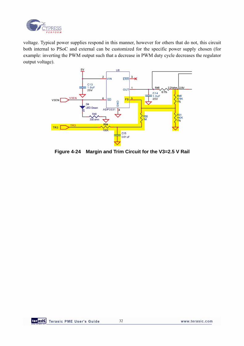
voltage. Typical power supplies respond in this manner, however for others that do not, this circuit both internal to PSoC and external can be customized for the specific power supply chosen (for example: inverting the PWM output such that a decrease in PWM duty cycle decreases the regulator output voltage).
Figure 4-24 Margin and Trim Circuit for the V3=2.5 V Rail
32

33
Margining is similar to trimming but is used for a different purpose. In that case, the rails are intentionally set to their upper or lower limits to enable system designers to verify that their systems work at both extremes of the voltage rail tolerances. For example, if a 5 V rail is used in the system and specified to have an accuracy of +/- 5%, margining will set the rail to 5 V -5% to enable system verification. Then the rail can be margined to the high side of 5 V +5% and the system verified again. This capability exists on all four rails controlled by PSoC in this example project.
Technical Details – Other Features
Example 2 also includes two other features, typically integrated into power supervisor applications: 1. I2C/SMBus/PMBus Interface to a Host CPU. (available on the white 5-pin header on PME
EBK) 2. EEPROM for calibration/configuration parameters, fault logging etc.
These components are both provided in the example project and are available for customization to meet application needs. Detailed description of how to make use of those features is not currently covered by this document. Example projects covering these topics in more detail will be added in the future.
Technical Details – Firmware Flowchart
The Voltage Sequencer component, window comparator fault detection circuit and fault handling interrupt service routine (ISR) for Example2 are identical to those described in Example1. The additional firmware flow required for Example2 is shown in the main loop flowchart (see Figure 4-25). The additions to the flow are summarized below:
1. Initialization of the PWM trim/margin hardware 2. Initializing and starting the first ADC conversion cycle 3. Periodically running the trim update (PWM adjust) algorithm 4. Handling I2C/SMBus/PMBus communications
In addition to the main loop flow described above, there is an additional thread that runs autonomously and asynchronously from the main loop. That is the ADC interrupt service routine (ISR) thread (see Figure 4-26). Once the first ADC conversion is initiated by the main loop firmware, the ADC end-of-conversion will generate an ADC ISR thread interrupt. That interrupt will handle reading of the raw count from the ADC, filtering, conversion to absolute units (mV or μA), checking voltage is within range, and then selecting the next analog input to connect to the ADC and changing the ADC range (between 0-4096 mV and +/- 256 mV) if required.

Display LCDIntro Message
Start Window ComparatorH/W Block
Check for EBKConnection
Start Voltage Sequencer Component
Enable Regulator n
Execute RampDelay for Slot n
PGOOD[n]OK?
Execute Up Delay for Slot [n]
n=n+1
n <= 4?
Handle User Interface
DisableAll Regulators
PGOODFailure Interrupt
Resetor Power On
n=1
Y
N
Y
Update TrimPWM Duty Cycles
Handle I2C/SMBus/PMBus
Transfers
Main Loop
Start PWM TrimCircuits
Start ADC Conversions
Figure 4-25 Example2 Firmware Main Loop Flowchart
34

Figure 4-26 Example2 ADC ISR Thread Firmware Flowchart
4.5 Power Management Component Library
The example projects provided use custom PSoC Creator components that are not included with the standard PSoC Creator Software install. These are the Voltage Sequencer, Comparator Controller and Comparator Glitch Filter Components. More information and additional example firmware for the Voltage Sequencer component is available in the following Application Note from Cypress: AN62496 - Voltage Sequencing with PSoC® 3 and PSoC® 5 The Comparator Controller and Comparator Glitch Filter custom components form part of the time-multiplexed window comparator and glitch filter circuit. Designers interested in using the window comparator and/or glitch filter will need to import those components in their own projects. The next section describes how to do that.
35

4.6 Using Components in Your Own Projects
NOTE: This section does not apply to PSoC Creator 2.0 or later as the required components are included in the tool component library. The Power Supervisor PSoC Creator components are provided in Library form so that you can easily add them to your own projects. To do so, you need to add the Library as a system dependency to your project. With your project open in PSoC Creator: 1. Under the Project Menu, select Dependencies 2. In the User Dependencies Area, select New Entry (the file icon) 3. Navigate to the KIT-035_Library.cylib directory (included in the example firmware distribution)
and select the KIT-035_Library.cyprj file. (open or double-click) 4. The component library should now be included in your project. Make sure that the
Components and Code check boxes are checked before closing the Dependencies dialog box
After adding the Component library to your project, there should be a Solutions tab in the Component Catalog containing the power supervisor components as shown below. These components can now be added to your own Creator design project schematic. (See Figure 4-27)
Figure 4-27 Solutions Component Catalog
36

Chapter 5 Schematics
5.1 Primary 12V Power Input
37

5.2 DVK Connector and Debug Test Points
5.3 Voltage Regulator V1=5V
38

5.4 Voltage Regulator V2=3.3V
5.5 Voltage Regulator V3=2.5V
5.6 Voltage Regulator V4=1.8V
39
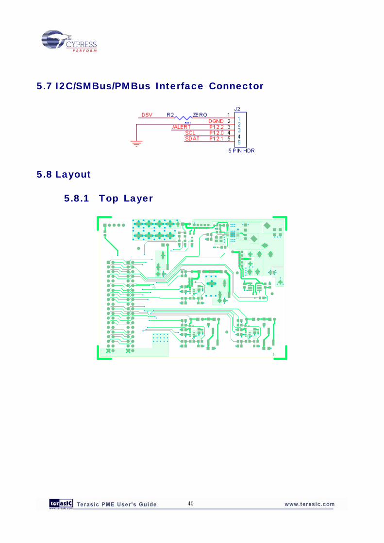
5.7 I2C/SMBus/PMBus Interface Connector
5.8 Layout
5.8.1 Top Layer
40

5.8.2 Ground Layer
5.8.3 Power Layer
41
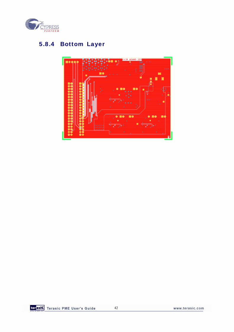
5.8.4 Bottom Layer
42

5.8.5 Top Silkscreen
43

44
5.9 Bill of Materials
Item Description Designator Quantity Value Manufacturer Manufacturer Part#
1 CAP .1UF 25V CERAMIC X7R 0805
C1,C4,C9 3 0.1μF,
25V
Kemet C0805C104K3RAC
7210
2 CAP CER 22UF
25V X5R 1206 C2,C5,C6 3 22μF,
25V Murata Electronics
North America GRM31CR61E226
KE15L 3 CAP CER 3300PF
50V 5% C0G 0805 C3 1 3.3nF,
50V
Murata Electronics
North America GRM2165C1H332J
A01D 4 CAP CER 1.0UF
25V 10% X5R
0805
C7,C10,C11,C13
C14,C16,C17 7 1.0μF,
25V
Murata Electronics
North America GRM216R61E105
KA12D
5 CAP CERM 39PF
5% 50V NP0 0805 C8 1 39pF,
50V
AVX Corporation 08055A390JAT2A
6 CAP CER
10000PF 50V
10% X7R 0805
C12,C15,C18 3 10nF,
50V
Murata Electronics
North America GRM216R71H103
KA01D
7 DIODE
SCHOTTKY 2A
20V SMB
D1 1 Vishay/General
Semiconductor SS22-E3/52T
8 LED GREEN
CLEAR 0805 SMD D2,D3,D4,D5 4 LITE-ON LTST-C170GKT
9 CONN HEADER
R/A DUAL 40POS
GOLD
J1 1 3M 961240-5604-AR
10 CONN HEADER
5POS .100 VERT
TIN
J2 1 Molex Inc 22-23-2051
11 CONN JACK
POWER 2.1mm
PCB RA
J3 1 CUI PJ-102A
12 BERGSTIK
II .100" SR
STRAIGHT
J5 1 FCI 68000-403HLF
13 CONN HEADER 2
POS .100 VERT
TIN
J6,J7,J8,J9,J10,
J11,J12,J13 8 Molex/Waldcom
Electronics Corp 22-28-4020
14 COIL PWR
CHOKE 22UH
L1 1 22μH,
2.2A
Panasonic - ECG ELL-ATV220M

45
2.2A SMD 15 RES 0.0 OHM
1/10W 5% 0805
SMD
R2,R8 2 Panasonic-ECG ERJ-6GEY0R00V
16 RES 51.0K OHM
1/8W 0.1% 0805
SMD
R3,R11,R13 3 51kΩ Susumu RG2012P-513-B-T
5
17 RES 20.0K OHM
1/8W 0.1% 0805
SMD
R4 1 22kΩ Susumu RG2012P-203-B-T
5
18 RES 2.21 OHM
1/16W 0.1% 0603
SMD
R5,R6,R7,R9,
R10,R15,R17,
R18,R19,R23,
R32,R33,
R35,R45,R56
15 2.21Ω Stackpole Electronics
Inc RNCF0603BKC2R
21
19 RES 1/10W 1K
OHM 0.1% 0805 R12 1 1kΩ Susumu RG2012P-102-B-T
5 20 RES 2.00K OHM
1/8W 1% 0805
SMD
R14,R37,R48,
R59 4 2kΩ Panasonic - ECG ERJ-6ENF2001V
21 RES 422 OHM
1/8W 1% 0805
SMD
R16 1 422Ω Panasonic - ECG ERJ-6ENF4220V
22 RES 100 OHM 2W
1% 2512 SMD R20,R21,R22,
R24 4 100Ω Stackpole Electronics
Inc RHC2512FT100R
23 RES 121K OHM
1/10W 1% 0603
SMD
R25 1 121kΩ Yageo RC0603FR-07121K
L
24 TRIMPOT 100
OHM 6MM SQ
SMD
R26,R38,R52,
R63 4 100Ω Bourns Inc. 3361P-1-101GLF
25 RES 330 OHM
1/16W 5% 0402
SMD
R27,R39,R49,
R60 4 330Ω Yageo Corporation RC0402JR-07330R
L
26 RES 22.1K OHM
1/10W 1% 0603
SMD
R28 1 22.1kΩ Yageo RC0603FR-0722K1
L
27 RES 100
OHM .5W 1%
1206 SMD
R29,R44,R47,
R55,R66 5 100Ω Vishay/Dale CRCW1206100RF
KEAHP
28 RES 100K OHM
1/8W 5% 0805
R30,R43,R54,
R65 4 100kΩ Panasonic - ECG ERJ-6GEYJ104V

46
SMD 29 RES 20K OHM
1/8W 5% 0805
SMD
R31 1 20kΩ Panasonic - ECG ERJ-6GEYJ203V
30 RES 33 OHM 2W
1% 2512 SMD R34 1 33Ω Stackpole Electronics
Inc RHC2512FT33R0
31 RES 634K OHM
1/8W 1% 0805
SMD
R36 1 634kΩ Panasonic - ECG ERJ-6ENF6343V
32 RES 1M OHM
1/10W 5% 0805
SMD
R40,R50,R61 3 1MΩ Panasonic - ECG ERJ-6GEYJ105V
33 RES 365K OHM
1/8W 1% 0805
SMD
R41 1 365kΩ Panasonic - ECG ERJ-6ENF3653V
34 RES 715 OHM
1/8W 1% 0805
SMD
R42 1 715Ω Panasonic - ECG ERJ-6ENF7150V
35 RES 475K OHM
1/8W 1% 0805
SMD
R46 1 475kΩ Panasonic - ECG ERJ-6ENF4753V
36 RES 442K OHM
1/8W 1% 0805
SMD
R51 1 442kΩ Panasonic - ECG ERJ-6ENF4423V
37 RES 1.07K OHM
1/8W 1% 0805
SMD
R53 1 1.07kΩ Panasonic - ECG ERJ-6ENF1071V
38 RES 340K OHM
1/8W 1% 0805
SMD
R57 1 340kΩ Panasonic - ECG ERJ-6ENF3403V
39 RES 51.0 OHM
1/4W 1% 1206
SMD
R58 1 51Ω Vishay/Dale CRCW120651R0F
KEA
40 RES 698K OHM
1/8W 1% 0805
SMD
R62 1 698kΩ Panasonic - ECG ERJ-6ENF6983V
41 RES 1.87K OHM
1/8W 1% 0805
SMD
R64 1 1.87kΩ Panasonic - ECG ERJ-6ENF1871V
42 TEST POINT 43
HOLE 65 PLATED
RED
TP1,TP3,TP4,
TP8,TP9,TP10 6 Keystone Electronics 5000

47
43 TEST POINT 43
HOLE 65 PLATED
BLACK
TP2,TP5,TP6,
TP7 4 Keystone Electronics 5001
44 IC AMP
CURRENT
SENSE 8-SOIC
U2 1 Maxim Integrated
Products MAX4080TASA+
45 HIGH-SIDE
CURRENT
MONITOR
U3 1 Zetex ZXCT1009FTA
46 IC CONV
STP-DWN SYNC
2A 14HTSSOP
U4 1 Texas Instruments TPS54226PWPR
47 IC REG LDO ADJ
200MA SOT-23-6 U5,U6,U7 3 Analog Devices Inc ADP3331ARTZ-RE
EL7 48 BUMPER
WHITE .500X.23
SQUARE
See Assembly
Drawing 4 Richco Plastics Co. RBS-3R
49 SHUNT GOLD
W/HANDLE,
BLACK
9 Kobiconn 151-8030-E
No Load Components
50 RES 1K 1/10W
OHM 0.1% 0805
R1 1 1kΩ Stackpole Electronics
Inc
RNCF0805BTC1K0
0
51 CONN HEADER
VERT DUAL
40POS GOLD
J4 1 3M 961240-6404-AR
52 HIGH-SIDE
CURRENT
MONITOR
U1 1 Zetex ZXCT1009FTA
53 TEST VIA 40
HOLE 20 PLATED
TV1,TV2,TV3,
TV4
4 NONE NA

Chapter 6 Appendix
6.1 Revision History
Version Change Log V1.0 Initial Version (Final)
6.2 Copyright Statement
Copyright © 2011 Terasic Technologies. All rights reserved.
48