Presentation on RFIC Mixer Design with ADS -...
37
This document is owned by Agilent Technologies, but is no longer kept current and may contain obsolete or inaccurate references. We regret any inconvenience this may cause. For the latest information on Agilent’s line of EEsof electronic design automation (EDA) products and services, please go to: www.agilent.com/find/eesof Agilent EEsof EDA
Transcript of Presentation on RFIC Mixer Design with ADS -...

This document is owned by Agilent Technologies, but is no longer kept current and may contain obsolete or
inaccurate references. We regret any inconvenience this may cause. For the latest information on Agilent’s
line of EEsof electronic design automation (EDA) products and services, please go to:
www.agilent.com/fi nd/eesof
Agilent EEsof EDA
nstewart
Text Box
Presentation on RFIC Mixer Design with ADS

1
Stephen LongProfessor, Electrical and Computer Engineering,University of California, Santa Barbara
RFIC Mixer Design with ADS

2
RFIC Mixer Design with ADS19 April, 2001
Page 2
About the Author
Steve Long
• University of California, Santa Barbara• Professor, Electrical and Computer Engineering
BIOGRAPHICAL SKETCHStephen Long received his BS degree in Engineering Physics from UC Berkeleyand MS and PhD in Electrical Engineering from Cornell University. He has beena professor of electrical and computer engineering at UC Santa Barbara since1981. The central theme of his current research projects is rather practical: useunconventional digital and analog circuits, high performance devices andfabrication technologies to address significant problems in high speedelectronics such as low power IC interconnections, very high speed digital ICs,and microwave analog integrated circuits for RF communications. He teachesclasses on communication electronics and high speed digital IC design.Prior to joining UCSB, from 1974 to 1977 he was a Senior Engineer at VarianAssociates, Palo Alto, CA. From 1978 to 1981 he was employed by RockwellInternational Science Center, Thousand Oaks, CA as a member of the technicalstaff.Dr. Long received the IEEE Microwave Applications Award in 1978 fordevelopment of InP millimeter wave devices. In 1988 he was a research visitor atGEC Hirst Research Centre, U.K. In 1994 he was a Fulbright research visitor atthe Signal Processing Laboratory, Tampere University of Technology, Finlandand a visiting professor at the Electromagnetics Institute, Technical University ofDenmark. He is a senior member of the IEEE and a member of the AmericanScientific Affiliation.

3
RFIC Mixer Design with ADS19 April, 2001
Page 3
Motivation – Why ADS for RFIC mixer design?
• Mixer DesignGuide provides analysis tools for:• DC, RF spectrum, impedance matching, gain, gain
compression, N_dB compression, IMD and TOI, noise figure,dynamic range, ACPR
• Parameter, frequency, RF and LO power sweeps
• Library of mixer examples
• Speeds up learning curve for ADS –• Become effective more quickly
• Set up complicated simulations that would take days toprepare in a few minutes
The mixer DesignGuide is intended to enhance productivity of RF designers byproviding an extensive collection of analysis tools that can be easily loaded intoyour project from a pulldown menu. Each pair of these analysis network anddisplays, which could take days to set up and verify, can be easily adapted foryour mixer circuit simulation requirements.

4
RFIC Mixer Design with ADS19 April, 2001
Page 4
• Design sequence very dependent on application• Upconversion application selected as example: base station
• Gilbert cell MOSFET double-balanced differential mixer
• 0.35 µm CMOS process; 3.3 volt supply
• Design for largest dynamic range
• Convert to single-ended output
Introduction
LO = 1.6 GHz
IFin = 200 MHz
RFout = 1.8 GHz Driver amplifier
A transmit mixer application is selected to illustrate a design procedure that isenabled by the Mixer DesignGuide. The input baseband or IF signal is centeredat 200 MHz. The output is at 1.8 GHz. We will assume that the mixer isintended for a base station power amplifier application.
The mixer will use 0.35 µm MOSFETs with a default device model parameter set.Of course, you will need to substitute your own verified MOSFET modelparameters for the default set. Otherwise, there would be no hope of anycorrespondence between simulation and measurement for the mixercharacteristics that are more sensitive to model nonlinearities. This wouldespecially be true for intermodulation simulations and noise.

5
RFIC Mixer Design with ADS19 April, 2001
Page 5
Learning Objectives:
• Learn how to make use of the Agilent ADS Mixer DesignGuide
• Understand the important design and analysis tools for thisapplication
• Specify performance: Gain, NF, P1dB, TOI, Dynamic Range
• Improve the design: add resonator and convert to single-endedoutput
Design a high dynamic range mixer fortransmit applications
Always see the NOTES pages for additional information throughout...
There are many different performance specifications for mixers. Some are ofinterest for receive applications where the input signal level is not under thecontrol of the designer. In this case, the maximum linearity under large signaldrive conditions is often very critical. Noise figure may be of secondary concern.
For the transmit application used here as an illustration, the designer has controlof the signal level. Then, the design strategy shifts to trading off noise and IMDbehavior in order to achieve the largest useable dynamic range.
As an extra illustration, after the intrinsic mixer performance is evaluated, thedesign will be modified to improve conversion gain and image rejection bytuning the mixer output. Secondly, a differential-to-single ended converter willbe added to interface to an off-chip bandpass filter.

6
RFIC Mixer Design with ADS19 April, 2001
Page 6
Using the ADS Mixer DesignGuide:First, select the analysis type...
The analysis tools are accessible by the DesignGuide pulldown menu. SelectMixer DesignGuide, then scroll through the list to find the relevant analysis.Then, the schematic and display panels will be loaded into your project.

7
RFIC Mixer Design with ADS19 April, 2001
Page 7
Differential Mixer Test Bench ExampleProceed by replacing the default mixer circuit with your mixerSet parameters and select the analysis schematic templatefrom the DesignGuide pulldown menu.
Passed parametersBiased mixer goes here
The mixer under test is constructed as an ADS subnetwork. The mixer itself canbe replaced with or modified to become your own design. Select the mixer, pushdown into the subnetwork, and replace the circuit with your own design. If youuse the Diff_MixerUnderTest as your subnetwork, and insert your design, thedesign is automatically inserted into all of the analysis circuit templates. Or, youcan save your design under a different name, select it using the componentlibrary icon on the toolbar, and replace the default mixer with your own.
You can declare any of the circuit parameters to be accessible outside of thesubnetwork by using the File > Design Parameters panel. In this example, VDD,RD (drain resistance), WCSP (current source control width), W1 and W2(transconductance and switch MOSFET widths), and source degenerationresistance (RS) and inductance (LS) are all available for a parameter sweep.

8
RFIC Mixer Design with ADS19 April, 2001
Page 8
Set up the simulation conditions
• Set variables and simulation controller sweep range
Set Order for the LO and RF inputs
You then will configure the simulation controller, HB in this example, with theappropriate parameters.Order[1] number of LO harmonics - should be large for switching mixersOrder[2] number of harmonics at the mixer signal input - small if inputamplitude is small; larger if you are simulating the mixer near the 1 dBcompression pointMaxOrder maximum sum of the LO and Input harmonics considered in thesolution. Generally, you would use the sum: Order[1]+Order[2]
SweepVar: This is the swept parameter, in this example the LO power. Set therange and step size used for the simulation.
Note that the data file size will increase with the order and with the number ofsweep steps.

9
RFIC Mixer Design with ADS19 April, 2001
Page 9
Gilbert cell double-balanced mixer
VDD
VRF output
VLO input
VIF input
Current source bias
Conversion gain, Gain compression,Bandwidth
Trade-offs:
VSS
I_bias
RS RS
RD
RD
W1 W1
W2 W2
WCS
Noise figure
Up conversion application example
We will utilize the DesignGuide mixer library as a starting point for the designexercise. This is a schematic of a MOSFET version of the Gilbert active double-balanced mixer. The lower FET diff pair serves as a transconductance amplifier.The upper FETs provide a fully balanced, phase-reversing current switch. A DCbias generator is included (not shown) which will keep the MOSFETs in theiractive region.The large signal handling capability of the mixer will depend mainly upon thelinearity of the transconductance amplifier, and is measured by determining themaximum input voltage (or power in some cases) that causes a 1 dBcompression in the conversion gain. The maximum linear input voltage rangecan be increased by increasing the source degeneration resistors, Rs. Whilesource inductance can also provide beneficial degeneration, in this case, wehave a very low input IF frequency, 200 MHz. The inductance values requiredwould be too large for RFIC implementation, thus we are stuck with the resistors(they will add noise). The load resistors could also cause gain compression ifthe voltage swing at the drains is large enough to cause the output to clip underlarge signal drive conditions.The double-balanced design rejects IF and LO feedthrough to the output if theoutput is taken differentially. This is because the LO component in the output isa common mode signal while the RF output is differential.For a more complete explanation of how the Gilbert cell mixer operates, refer tothe reference list at the end of this presentation.

10
RFIC Mixer Design with ADS19 April, 2001
Page 10
Design procedure
1. LO amplitude: Conversion gain, Vin at 1 dB gain compression
2. Gain Compression: source resistance Rs, drain resistance, Rd
3. Noise figure: Rs, I_bias
4. Dynamic Range vs. Input Voltage
5. Spectral spreading and ACPR with digital modulation
The example design sequence is suited for an upconversionmixer. Our goal is to increase dynamic range. Conversion gainand matching are not as critical.
A mixer that is to be used for base station transmit applications requires highlinearity and low noise so that the least amount of spurious power is spread intothe adjacent channel. We will optimize our mixer in the following sequence:1. LO amplitude. You want to make sure the mixer commutating switch is fullyactivated. Excess distortion can be produced with a weakly conducting orslowly activated switch. Use the conversion transducer gain and 1 dB gaincompression input level to determine when the LO voltage is sufficient.2. Evaluate the influence of source and drain resistance on the 1 dBcompression level. This will give insight into the principal mechanisms that limitlinearity.3. The added noise of the mixer will affect the minimum signal level and thuslimit dynamic range. There will be a tradeoff between noise, gain, and gaincompression.4. The two-tone 3rd order intermodulation distortion power and the noise figuredetermine the mixer dynamic range vs. input voltage. Since for transmitapplications you have complete control over your input voltage, find the optimumdynamic range - the mixer’s “sweet spot” for best performance. Or,alternatively, if you have a fixed signal level, design the mixer to provide the bestdynamic range at that signal level.5. Finally, test the mixer under more realistic signal excitation - using a CDMAsource, for example, to emulate a multicarrier environment. This is a moresevere test than the two-tone IMD one, and is much more time consuming tosimulate since a large number of symbols must be used for accurate results.

11
RFIC Mixer Design with ADS19 April, 2001
Page 11
Design sequence
VSS
I_bias
RS RS
RD RD
W1 W1
W2 W2
WCS
VSS
I_bias
RS RS
RD RD
W1 W1
W2 W2
WCS
Gilbert cell - resistively loaded
Resonator at output
RSRS
VDD
RL RL
RSRS
VDD
RL RL
D2SE
Convert to single-ended output
Let’s get started!
Once the basic resistively loaded Gilbert cell mixer is characterized, twomodifications will be employed to improve performance. First, the mixer drainnodes will be tuned with inductors and a capacitor for resonance at the outputfrequency. This improves conversion gain if inductors with reasonable Qu canbe fabricated. It also decreases the amplitude of the undesired output imagebecause of its bandpass transfer function. The image must be removed anyway,and it’s presence can only degrade the distortion of the output stage byincreasing the peak voltage present at its input.
The output of the mixer will need to be filtered off-chip with a SAW filter beforefurther amplification, so a single ended output is more efficient. The last stageis added to perform a differential to single ended conversion. It must have goodcommon mode rejection to suppress LO feedthrough and good linearity so that itdoesn’t degrade dynamic range.

12
RFIC Mixer Design with ADS19 April, 2001
Page 12
1. Determine LO voltage: Conversion gain & gaincompression• Sweep LO power
• Conversion gain – PLO
• Gain Compression – P1dBUp
Down
The first step is to determine a suitable LO voltage that provides a reasonablecompromise between conversion gain and LO power and at the same time doesnot limit the 1 dB gain compression input voltage. The MOSFETs forming thecommutating switch (upper level) must be driven hard enough to present a lowseries resistance to the load. Most of the mixer analysis schematic and displaytemplates available in the DesignGuide library include an LO power sweepcapability. Use the menu as shown to select a conversion gain simulation as afunction of LO power. Also, a NdB Gain Compression analysis can be used toevaluate the dependence of gain compression on LO drive.
From these simulations, we see that the input power at which gain compressesby 1 dB (P1dB) is not a strong function of LO voltage, but conversion gain issomewhat dependent. The more gate voltage applied to the upper tier ofMOSFETs, the lower their series resistance relative to the drain resistance andthus the higher the conversion gain. We also can see that there is a conversionloss which gets worse at the higher output RF frequency of 1.8 GHz, but we canimprove on this later by tuning the RF output of the mixer.

13
RFIC Mixer Design with ADS19 April, 2001
Page 13
2. V1dB dependence on RS, RD
• We can see a strong dependence of gain compression on Rs
• RD has little effect on compression, so limiting is occurring at theinput
RS
RD
Nearly constant
Gain compression is evaluated using the N-dB Gain Compression Point analysisschematic. The 1dB gain compression input power and input voltage are foundfor swept parameters. In this case, the influence of RS and RD on V1dB wasdetermined. The RS sweep used RD = 100Ω. The RD sweep set RS = 30Ω.Conversion gain is measured at the 1 dB compressed level. Alternatively, a two-dimensional sweep could also be set up using an extra Parameter Sweepcontroller.In an RFIC mixer where the input might not be matched to a source impedance,the input voltage is a more important metric of gain compression than the inputavailable power (P1dB) since available power assumes a conjugately matchedsource and load. Also, in a multi-signal environment, the peak input voltage canbe quite large at the instant in time when all signals add in phase. It is this peakvoltage that determines the distortion limits of the mixer. For example, the two-tone IMD simulations will predict a 1 dB compression power 6 dB lower thansingle tone simulations because the peak voltage will be twice as high for thesame power per tone.
It is also interesting to note that the conversion power gain depends inverselyon RD. In the simulation, the external load resistance was set to 2 RD so that theoutput power (power absorbed in the load) is also the available output power,Pout = Vout
2/4RD. The voltage gain would be expected to follow RD/RS butincreases less rapidly than anticipated, probably due to the output RC timeconstant bandwidth limitations.
14
RFIC Mixer Design with ADS19 April, 2001
Page 14
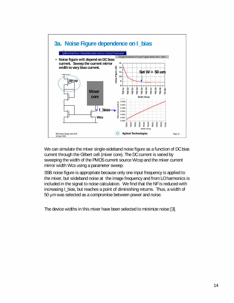
• Noise figure will depend on DC biascurrent. Sweep the current mirrorwidth to vary bias current.
3a. Noise Figure dependence on I_bias
I_bias
Set W = 50 µm
Mixer core
Wcsp
Wcs
We can simulate the mixer single-sideband noise figure as a function of DC biascurrent through the Gilbert cell (mixer core). The DC current is varied bysweeping the width of the PMOS current source Wcsp and the mixer currentmirror width Wcs using a parameter sweep.SSB noise figure is appropriate because only one input frequency is applied tothe mixer, but wideband noise at the image frequency and from LO harmonics isincluded in the signal to noise calculation. We find that the NF is reduced withincreasing I_bias, but reaches a point of diminishing returns. Thus, a width of50 µm was selected as a compromise between power and noise.
The device widths in this mixer have been selected to minimize noise [3].

15
RFIC Mixer Design with ADS19 April, 2001
Page 15
3b. Noise Figure dependence on Rs
• The noise figure will also be strongly affected by Rs.
• We find that we must trade off NF and V1dB. This will influence dynamicrange
• Noise floor = MDS = -174 dBm/Hz + 10 log BW + NF• Conversion gain is also varied, and may affect input referred noise
We also find a strong dependence of SSB NF on the source resistance. This isexpected because the thermal noise contributed by the resistor is directly in theinput voltage loop of the differential pair. Thus, we will need to trade off V1dBand noise figure to obtain the largest dynamic range of the mixer.
The dynamic range at low input signal power levels will be limited by the carrierto noise ratio. The noise power for a minimum detectable signal (S/N = 1)depends on both NF and the noise bandwidth. This bandwidth will normally beset by an external SAW filter between the mixer and the driver amplifier. Thefilter is also required to reject the output difference (FLO – FIN) image frequencyat 1.4 GHz.
The conversion gain (a loss in this case) may also increase the noise figurebecause the drain resistor thermal noise is input referred through the gain.Thus, we will also want to investigate a tuned output to eliminate some of thisnoise.

16
RFIC Mixer Design with ADS19 April, 2001
Page 16
3c. Noise Figure dependence on RS, RD
• You can perform a two parameter sweep and plot contours of noisefigure.
6 dB
7 dB
8 dB
9 dB
You can also perform a two parameter sweep by selecting a second ParameterSweep controller. In this example, the variation in noise figure with RS and RDthat was displayed in tables on the previous slide can now be plotted asconstant NF contours using the contour function in the function library.

17
RFIC Mixer Design with ADS19 April, 2001
Page 17
3d. Up Conversion Gain dependence on RS, RD
• And also a contour plot for conversion gain:
-5 dB
-7 dB
-9 dB
You can do the same thing with the conversion gain data.

18
RFIC Mixer Design with ADS19 April, 2001
Page 18
4a. Carrier to IMD ratio• Both carrier/noise and carrier/IMD can limit dynamic range
• Determine the 3rd order IMD power vs. input voltage or powerwith 2-tone HB simulation.
Noise Floor (MDS)
At higher input signal levels, the dynamic range of the mixer is limited by thedistortion. The third-order intermodulation distortion products are the mostdamaging because they show up in-band and cannot be rejected by the filter.A two-tone third-order IMD simulation with an RF power sweep can be used todisplay the carrier-to-IMD power ratio. The IMD power present in the output willincrease at 3 times the rate of increase of input power. Thus, the differencebetween output power and IMD power shrinks with increasing input.At low input signal levels, the noise floor, set by the mixer noise figure and thenoise bandwidth of the mixer-bandpass filter-amplifier cascade, will set a lowerlimit to the output power from the mixer. The dotted lines above show thisnoise floor in red. The blue dotted line represents the mixer output power vs. RFinput power at this lower input regime. It has a slope of 1. You can see that thedifference between output power and noise floor shrinks as the powerdecreases.
The maximum dynamic range is found at the inflection point.

19
RFIC Mixer Design with ADS19 April, 2001
Page 19
4b. Calculate dynamic range vs input voltage
• Combine data from IMD RF power sweep and SSB NF simulations
• Plot dynamic range for RS = 30Ω
C/Nlimited
C/IMDlimited
IF input voltage*NOTE: step 5 comes later, but first...
Here, we have taken outputs from two simulations: IMD RF power sweep andthe SSB NF. The dynamic range is controlled by the least of these twoconditions:
DR = Pout (dBm) – MDS (dBm) for low input levels (noise limited)
DR = Pout (dBm) – PIMD (dBm) for higher input levels (distortion limited)
Rs DR (dB) Vin (V) NF (dB)(differential)
10 57.7 0.017 6.520 57.3 0.025 830 56.4 0.031 9.240 56.0 0.039 10.3
The dynamic range peak will depend on the noise bandwidth. For narrowerbandwidths, the noise floor will drop and the peak DR will increase but shift tolower differential input voltage. The 30 MHz noise bandwidth was chosenbecause of the base station application. The transmitter should be capable ofcovering an entire frequency band.

20
RFIC Mixer Design with ADS19 April, 2001
Page 20
Improve mixer conversion gain and noise figure
• Tune the output of the mixer
• Absorb capacitance
• Frequency sweep
1.8 GHz
1.4 GHz
1.4 GHz
1.8 GHz
Resistive load
Tuned
The low conversion gain of the resistively loaded mixer will cause higher noisedue to the drain resistors. By resonating the output at 1.8 GHz, the conversiongain is increased and the gain at the image (1.4 GHz) is reduced. Thecomparison between the resistive loaded case and the tuned case shows anincrease in conversion gain by about 3.5 dB.You can perform an RF frequency sweep to find the resonant frequency. Fromthat, you can calculate how much capacitance is contributed by the drain-to-substrate junction and absorb it into the resonator.An unloaded Q = 5 is assumed for the inductor.

21
RFIC Mixer Design with ADS19 April, 2001
Page 21
Gain reduction due to inductor Q
• We do find, however, that the gain is sensitive to the unloaded Q ofthe inductor. Rind represents the series resistance of the inductor.
• Q unloaded is varied from 12 down to 5.
Rind
L
Rind
On chip inductor Q is limited by metal losses and substrate conduction in bulksilicon processes. An ordinary digital IC process will produce low Qu in spiralinductors. CMOS or BiCMOS RFIC processes can achieve higher Q inductors byusing thicker dielectrics and thicker metal. Q values in the range of 5 to 15 aretypical.
The low conversion gain is also due in both cases to an unmatched input. Wewill consider this later.

22
RFIC Mixer Design with ADS19 April, 2001
Page 22
Tuned output - noise figure
• The noise figure is reduced by about 0.5 to 1 dB whenthe output of the mixer is tuned. Again, this dependson the inductor Q.
RD = 2.5 RL = 400Unfortunately, for realistic unloaded inductor Q values (on bulk Silicon) of theorder of 5, the benefits of tuned output are diminished. The conversion gain isimproved by about 4 dB and the noise figure by only 0.5 dB. There would bemuch more benefit on a CMOS RF Analog, SOI or GaAs processes where higherQ values can be obtained.Having said that, we will continue to evaluate the tuned solution.

23
RFIC Mixer Design with ADS19 April, 2001
Page 23
• Connect differential amplifier stage tooutput of tuned mixer.
• Choose either direct output as shown(with off-chip load resistor) or use asource follower.
• Size the MOSFETs according to theoutput current and voltage required.Their input capacitance can be absorbedin the mixer tank circuit.
• Determine RS_D2S so that the D2SE blockdoes not degrade the dynamic range.
Active Balun: differential to single-ended RF out
RS_D2S RS_D2S
VDD
RL RL
D2SE
The next step will be to convert the RF output from a differential signal to single-ended with an active balun. You must perform this conversion rather than justtaking one output from the mixer because the mixer differential output isnecessary for rejection of LO feedthrough. Since we need a SAW filter betweenthe mixer output and the driver stage, a single-ended output is sufficient. Whilepassive baluns can be made for 1.8 GHz, we will benefit in cost and size byplacing an active balun on-chip. This differential amplifier stage is used toconvert the differential output of the tuned mixer to a single output. The gatecapacitances of the D2SE stage can be absorbed into the resonator at the mixerdrain nodes. The D2SE stage must also be designed so that it does not dominatethe IMD generation of the mixer. RS_D2SE can be adjusted to set the V1dB level.The output driver could use an off-chip load resistor with open drain outputconnection as suggested by the circuit simulated here. The load resistance willprobably be determined either by the filter impedance or by transmission lineimpedance. The bias current for the D2SE converter stage will be dictated bythis impedance level. The device widths must also be chosen so that they canhandle the necessary drain current and provide adequate voltage gain. Theaddition of a source follower to the output is another option.

24
RFIC Mixer Design with ADS19 April, 2001
Page 24
Evaluate mixer with D2SE stage
• First simulate with differential mixer analysistools to compare with resistively loaded andtuned mixer performance
– Noise figure and conversion gain
– IMD and dynamic range
• Then, adapt single-ended (SE) mixer analysistools from the DesignGuide to evaluate with SEinput and output
For the initial design evaluation, we will continue to measure the differentialoutput so that comparisons can be made between the differential tuned mixerand the mixer with output buffer. Then, the mixer will be evaluated in a single-ended configuration.

25
RFIC Mixer Design with ADS19 April, 2001
Page 25
Noise Figure and Conversion Gain Contours
1 dB
3 dB
5 dB
7 dB9 dB
7 dB
8 dB9 dB
6 dB
• Large dependence ofgain and NF on RS
• Gain very dependenton Rind
The SSB noise figure simulation is performed again with parameter sweeps forRS and Rind. We can see that there is little noise sensitivity to Rind, however, itstrongly affects the conversion gain. RS affects both NF and conversion gainand it also will also affect the carrier-to-IMD ratio vs. IF input voltage.

26
RFIC Mixer Design with ADS19 April, 2001
Page 26
Dynamic range simulations
• Dynamic range vs. RS ofmixer. Rind = 5 Ω
• Noise figure dominates overthe IMD behavior at thisbandwidth since DRimproves with smaller RS
• Dynamic range alsoimproves with reduction inRind.
2259.29.730
1759.88.520
1260.5710
Vin (mV)DR (dB)NF (dB)RS
The Mixer TOI/IMD simulation is performed again for RS of 10, 20, and 30 ohms.We can see that the dynamic range slowly improves for smaller RS. This will bevery dependent on the noise bandwidth, however. For our simulations, a 30MHz bandwidth was assumed.

27
RFIC Mixer Design with ADS19 April, 2001
Page 27
Test as single ended mixerModify SE schematic to evaluate our mixer
Copy from differentialtest schematic
Terminate unused I/Os
A DesignGuide schematic intended for evaluation of single-ended mixers wascopied from the menu and modified. Our tuned mixer with the D2SE outputstage was inserted from the component library. Unused inputs were terminated:the input was grounded and the output terminated in a large resistance.The LO is differential. A transformer and source was copied from a differentialtest schematic and pasted into this schematic. An active LO SE to differentialstage could also be designed and added to the mixer if desired.

28
RFIC Mixer Design with ADS19 April, 2001
Page 28
Single-ended NF and IMD performance
• NF higher; CG lower thandifferential mixer
• Use NF and IMD vs RF powerto calculate dynamic rangefor the single-ended mixerconnection
Again, noise figure and IMD vs RF power sweeps were performed for a range ofRS values from 10 to 30 ohms. This is combined to determine dynamic range onthe next slide.

29
RFIC Mixer Design with ADS19 April, 2001
Page 29
Single-ended mixer: dynamic range
The best result was for the RS = 10 ohm case. We see a peak dynamic range of57.5 dB at an input voltage of 14 mV.
30
RFIC Mixer Design with ADS19 April, 2001
Page 30
5. Simulate mixer with CDMA input
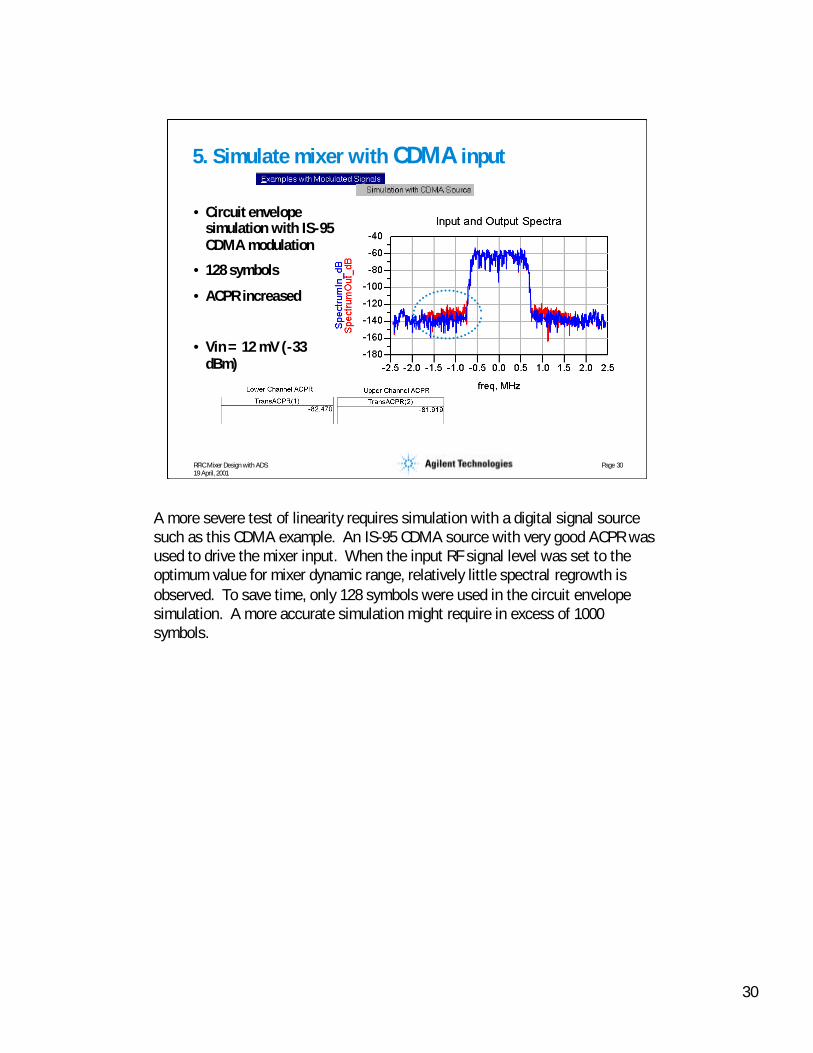
• Circuit envelopesimulation with IS-95CDMA modulation
• 128 symbols
• ACPR increased
• Vin = 12 mV (-33dBm)
A more severe test of linearity requires simulation with a digital signal sourcesuch as this CDMA example. An IS-95 CDMA source with very good ACPR wasused to drive the mixer input. When the input RF signal level was set to theoptimum value for mixer dynamic range, relatively little spectral regrowth isobserved. To save time, only 128 symbols were used in the circuit envelopesimulation. A more accurate simulation might require in excess of 1000symbols.

31
RFIC Mixer Design with ADS19 April, 2001
Page 31
Evaluate at higher drive level
• Input available powerincreased to –25 dBm
• Effects of IMDgeneration and gaincompression effects areevident with widebandsource – ACPR is muchhigher
When the signal level is increased, there is much more distortion evident. Theinput level in this simulation corresponds to about 30 mV of drive voltage.

32
RFIC Mixer Design with ADS19 April, 2001
Page 32
IF input impedance
• The RF input port impedance can be matched if baseband/IFgeneration is from off-chip.
• We can see at 200 MHz, the input impedance is dominated bycapacitive reactance.
We noted earlier that the input of the mixer is badly mismatched. This may notbe of much concern if the baseband and IF driver circuits are on the same chipwith the upconversion mixer. In that case, the voltage levels are more ofinterest.
If you are interested in driving from off chip, we can see above that the inputimpedance is dominated by capacitive reactance. A matching network couldincrease the conversion gain significantly if this were of interest.

33
RFIC Mixer Design with ADS19 April, 2001
Page 33
Impedance matching utility
• Specify Zdesired = Zin*
The Mixer DesignGuide contains several impedance matching utilities that couldbe used to design and evaluate matching networks.

34
RFIC Mixer Design with ADS19 April, 2001
Page 34
Conclusion
• Learn how to make use of the Agilent ADS MixerDesignGuide
• Understand the important design and analysis tools for thisapplication
• Specify performance: Gain, NF, P1dB, TOI, Dynamic Range
• Improve the design: add resonator and convert to single-ended output
Learning objectives met:
We have now completed a design study of an upconversion transmit mixer. Theprocedure illustrated here is by no means unique, and you may find ways ofgetting the same information by other sequences of steps.
Also, the DesignGuide analysis schematics can be further modified to includenested sweeps. These can provide a two-dimensional perspective on the designspace to gain further insight (in exchange for increased simulation time and datafile size).
You can also make use of the ADS optimizer to automatically achieve the designgoals. This could require combining the simulations on more than one analysisschematic onto a single multi-level schematic, or possibly creating a look-uptable and interpolation function for one of the critical performance parameters tospeed up the optimization process.
35
RFIC Mixer Design with ADS19 April, 2001
Page 35
References
• Gray, P. R. and Meyer, R. G., Design of Analog Integrated Circuits, 4th Ed.,Chap. 10, Wiley, 2001.
• Gilbert, B., “Design Considerations for BJT Active Mixers”, AnalogDevices, 1995.
• Lee, T. H., The Design of CMOS Radio-Frequency Integrated Circuits, Chap.11, Cambridge U. Press, 1998.
• Agilent EESof Design Seminar, “Fundamentals of Mixer Design,” 1999.
• Agilent EESof Design Seminar, “RFIC Mixer Design”, 1999.

www.agilent.com/fi nd/emailupdatesGet the latest information on the products and applications you select.
www.agilent.com/fi nd/agilentdirectQuickly choose and use your test equipment solutions with confi dence.
Agilent Email Updates
Agilent Direct
www.agilent.comFor more information on Agilent Technologies’ products, applications or services, please contact your local Agilent office. The complete list is available at:www.agilent.com/fi nd/contactus
AmericasCanada (877) 894-4414 Latin America 305 269 7500United States (800) 829-4444
Asia Pacifi cAustralia 1 800 629 485China 800 810 0189Hong Kong 800 938 693India 1 800 112 929Japan 0120 (421) 345Korea 080 769 0800Malaysia 1 800 888 848Singapore 1 800 375 8100Taiwan 0800 047 866Thailand 1 800 226 008
Europe & Middle EastAustria 0820 87 44 11Belgium 32 (0) 2 404 93 40 Denmark 45 70 13 15 15Finland 358 (0) 10 855 2100France 0825 010 700* *0.125 €/minuteGermany 01805 24 6333** **0.14 €/minuteIreland 1890 924 204Israel 972-3-9288-504/544Italy 39 02 92 60 8484Netherlands 31 (0) 20 547 2111Spain 34 (91) 631 3300Sweden 0200-88 22 55Switzerland 0800 80 53 53United Kingdom 44 (0) 118 9276201Other European Countries: www.agilent.com/fi nd/contactusRevised: March 27, 2008
Product specifi cations and descriptions in this document subject to change without notice.
© Agilent Technologies, Inc. 2008
For more information about Agilent EEsof EDA, visit:
www.agilent.com/fi nd/eesof
nstewart
Text Box
Printed in USA, April 19, 2001 5989-9104EN