Presentation on RFIC MOS Gilbert Cell Mixer...
46
This document is owned by Agilent Technologies, but is no longer kept current and may contain obsolete or inaccurate references. We regret any inconvenience this may cause. For the latest information on Agilent’s line of EEsof electronic design automation (EDA) products and services, please go to: www.agilent.com/find/eesof Agilent EEsof EDA
-
Upload
duongthuan -
Category
Documents
-
view
240 -
download
1
Transcript of Presentation on RFIC MOS Gilbert Cell Mixer...

This document is owned by Agilent Technologies, but is no longer kept current and may contain obsolete or
inaccurate references. We regret any inconvenience this may cause. For the latest information on Agilent’s
line of EEsof electronic design automation (EDA) products and services, please go to:
www.agilent.com/fi nd/eesof
Agilent EEsof EDA
nstewart
Text Box
Presentation on RFIC MOS Gilbert Cell Mixer Design

1
H•4/17/01
DDesignesignSSeminareminar
Agilent EEsof Agilent EEsof Customer EducationCustomer Educationand Applicationsand Applications
RFIC MOS Gilbert Cell Mixer Design
Abstract
The Gilbert double-balanced mixer configuration is widely used in RFIC applications because of its compact layout and moderately high performance. This seminar will walk through the design of a CMOS Gilbert mixer focusing on the parameters that influence the linearity of the signal path, the noise, and therefore the spurious-free dynamic range of the mixer. We will explore design tradeoffs that include biasing and device sizing, LO power, conversion gain, gain compression, intermodulation distortion, and noise.

2
H•4/17/01
Page 2
About the Author
Steve Long
• University of California, Santa Barbara • Professor, Electrical and Computer Engineering • Consultant to Industry
BIOGRAPHICAL SKETCH
Stephen Long received his BS degree in Engineering Physics from UC Berkeley and MS and PhD in Electrical Engineering from Cornell University. He has been a professor of electrical and computer engineering at UC Santa Barbara since 1981. The central theme of his current research projects is rather practical: use unconventional digital and analog circuits, high performance devices and fabrication technologies to address significant problems in high speed electronics such as low power IC interconnections, very high speed digital ICs, and microwave analog integrated circuits for RF communications. He teaches classes on communication electronics and high speed digital IC design.
Prior to joining UCSB, from 1974 to 1977 he was a Senior Engineer at Varian Associates, Palo Alto, CA. From 1978 to 1981 he was employed by Rockwell International Science Center, Thousand Oaks, CA as a member of the technical staff.
Dr. Long received the IEEE Microwave Applications Award in 1978 for development of InP millimeter wave devices. In 1988 he was a research visitor at GEC Hirst Research Centre, U.K. In 1994 he was a Fulbright research visitor at the Signal Processing Laboratory, Tampere University of Technology, Finland and a visiting professor at the Electromagnetics Institute, Technical University of Denmark. He is a senior member of the IEEE and a member of the American Scientific Affiliation.

3
H•4/17/01
Page 3
Basic engineering problem:
• Understand operation of MOSFET Gilbert mixer
• Biasing considerations
• Design for stability, linearity and noise
• Specify performance: NF, P1dB, TOI, SFDR
Design of MOS RFIC mixers for large dynamic range...
Learning Objectives:
Always see the NOTES pages for Exercises throughout...
There are many different mixer circuit topologies and implementations that are suitable for use in receiver and transmitter systems. We will select one of the widely used double-balanced mixer topologies as our example. The design process presented here will have more general applicability to other circuit approaches, both for mixers and amplifiers, in receiver applications.

4
H•4/17/01
Page 4
Design specifications
• Frequencies:
• LO = 855 MHz
• RF = 900 MHz
• IF = 45 MHz
• Technology: 0.35 µm CMOS
• Supply voltage: 3.3V
• Input IP3 > − 6 dBm
• RF Input: matching off chip on PCB; single-ended
• LO Input: single-ended; on-chip LO buffer
Here we have some representative, but somewhat arbitrary specifications for the mixer.
A BSIM 3.3 model was used for the 0.35 µm CMOS process. Parameters for the model were obtained from a digital CMOS process, so absolute accuracy for more analog applications involving distortion and noise is not to be assumed. But, relative accuracy is sufficient for exploring many of the design details and revealing general trends.

5
H•4/17/01
Page 5
Ideal Double Balanced Mixer
-gm +gm
RF input
LO Input
+V
IF output
•Switch polarityof RF current
•Linear V -> Iconversion
•Linear I -> VconversionRL RL
An ideal double balanced mixer simply consists of a switch driven by the local oscillator that reverses the polarity of the RF input at the LO frequency[1]. To get the highest performance from the mixer we must make the RF to IF path as linear as possible and minimize the switching time of the LO switch. The ideal mixer above would not be troubled by noise (at the low end of the dynamic range) or intermodulation distortion (IMD) at the high end since the transconductors and resistors are linear and the switches are ideal.
The ideal balanced structure above cancels any output at the RF input frequency since it will average to zero. It also cancels out any LO frequency component since we are taking the IF output as a differential signal and the LO shows up as common mode. Therefore, to take full advantage of this design, an IF balun, either active (a differential amplifier) or passive (a transformer or hybrid), is required.

6
H•4/17/01
Page 6
How does it convert frequency?
• Let VRF(t) = VR cos (ωRFt)
• The circuit converts this into a current:
I = gmVRF(t)
• Then, it multiplies I by the LO switching function T(t) defined in the next slide.
• VIF(t) = 2 gm RL T(t) VRF(t) = A T(t) VRF(t)
Mixers perform frequency translations (conversion) by multiplication of an RF input signal with an LO signal. The trig relationship
cos x sin y = (1/2) [sin(x + y) - sin(x - y)]
provides the desired up and down translations.

7
H•4/17/01
Page 7
LO Switching Function T(t)
+++−=
+++=
....)3sin(31
)sin(2
21
)(
....)3sin(31
)sin(2
21
)(
2
1
tttT
tttT
LOLO
LOLO
ωωπ
ωωπ
T1(t)
T2(t)
T(t) = T1(t) + T2(t)
SUM OF SWITCHING FUNCTIONS
If the LO is a square wave with 50% duty cycle, it is easily represented by its Fourier Series. The symmetry causes the even-order harmonics to drop out of the LO spectrum. When multiplied by a single frequency cosine at ωRF the desired sum and difference outputs will be obtained as shown in the next slide.
There will be harmonics of the LO present at 3ωLO, 5ωLO, etc. that will also mix to produce outputs called “spurs” (an abbreviation for spurious signals).

8
H•4/17/01
Page 8
IF Output Spectrum
[ ]ttAV
LORFLORFR )sin()sin(
2ωωωω
π−−+
No odd-order productsin ideal DB mixer
[ ]...)5sin()3sin()sin()cos()( 51
314
+++= ttttAVtV LOLOLORFRIF ωωωω π
Second order:
upconversion downconversion
ωLOωLO - ωRF ωLO + ωRF 3ωLO3ωLO - ωRF 3ωLO + ωRF
Fourth order:
The second-order output spectral lines at ωLO ± ωRF are the desired upconversion and downconversion products from the mixer. Typically, one of these outputs will be removed by IF filtering. Note that ideally there will not be any third-order or higher odd-order products in the mixer output since only odd LO harmonics are generated in a perfectly symmetric switching DBmixer. The DC component should also cancel. This reduces the number of spurious outputs when compared with other nonlinear or unbalanced mixer approaches making the selection of the LO and IF frequencies less restrictive.
Here we see that the ideal conversion gain (VIF/VR)2 = A2 (2/π)2 = − 4 dB
(if A=1).
In real mixers, there is always some imbalance. This will produce some LO to IF or RF to IF feedthrough (thus, isolation is not perfect). Secondly, the RF to IF path is not perfectly linear. This will lead to intermodulation distortion. Odd-order distortion (typically third and fifth order are most significant) will cause spurs within the IF bandwidth or cross-modulation when strong signals are present. Also, the LO switches are not perfectly linear, especially while in the transition region. This can add more distortion to the IF output and will increase loss due to the resistance of the switches.

9
H•4/17/01
Page 9
Intermodulation distortion
• IMD consists of the higher order signal products that are generated when two RF signals are present at the mixer input. The IMD will be down and up converted by the LO as will the desired RF signal.
• IMD generation is a good indicator of large signal performance of a mixer.
• Absolute accuracy is highly dependent on the accuracy of the device model, but the relative accuracy is valuable for optimizing the circuit parameters for best IMD performance.
Next we would like to evaluate how the distortion generated by the mixer signal path is affected by the choice of various design parameters.

10
H•4/17/01
Page 10
Design of MOS DB mixer
• Device width
• Biasing
• Linearity of transconductance amplifier
• Stability and input matching network
• Gain compression and IMD
• Noise figure
• Spurious Free Dynamic Range
Our approach will emphasize the distortion-limited (large-signal) performance over noise-limited (small-signal) performance.

11
H•4/17/01
Page 11
Active MOS DB Mixer
VDD
VIF Output
VLO Input
VRF Input
Current source bias
VSS
I_bias
RS RS
RL RL
W1 W1
W2 W2
WCS
This is a schematic of a MOSFET version of the Gilbert active DB mixer (Gilbert claims that it was really first invented by H. E. Jones as a demodulator).[2] The upper FETs provide a fully balanced, phase-reversing current switch function. The lower FETs are the transconductance amplifier.
Many design decisions are possible.
I_bias and device widths W1 and W2: We need to choose a W1 that will provide high gm, saturation at low VDS (for low power supply operation), and low noise. Large widths are preferred for noise, and the optimum width for noise with power constraints can be estimated from the MOS device parameters [3]. Large widths also require large bias currents to obtain high gm. Choosing W1 = W2 is typically best. So, next we must investigate the minimum current required to keep all devices in saturation.
Linearity of signal path: Once the bias is determined, we will investigate linearization of the transconductance amplifier through source resistance and inductance. Resistance will increase the input voltage range where nearly linear gain can be obtained, but will reduce conversion gain to some degree. Source inductance will be used mainly to guarantee stability by forcing a positive real component into the input impedance. This also helps to make the input impedance easier to match.

12
H•4/17/01
Page 12
Device width and bias current
• Width is estimated for noise[3]:
• for CMOS with L = 0.35 µm
and Rgen= 50Ω: Wopt = 800 µm
• Determine suitable bias current• require: VDS > VDsat
• caution: VSB varies with current
• use differential amp to evaluate
device I-V & gm. Use I_bias as
the independent variable.
genoxopt RLC
Wω3
1≈
I_bias
RL
W1
WCS
IDS
VGS
+−
VDD
VinVref
The device width of 800 µm is estimated from a MOSFET noise model[3]. For this width, you must make sure that IDS is large enough to saturate the MOSFET (VDS > Vdsat). At the same time, you want to design for low VDDoperation, so large VDS is also undesirable. Finally, large VDS will increase hot electron effects at the drain thereby increasing noise.
Exercise: set up a DC simulation of a MOSFET with width of 800 µm and gate length of 0.35µm using the ADS design file MOS_curve_tracer.dsn. Note the size of Vdsat for various gate voltages. Apply a positive source-to-substrate (bulk) potential and see how the device current varies with VSB. This body effect will increase the threshold voltage VT and reduce current for a given VGS.
When I_bias is swept on the diff amp above, the source-to-bulk voltage changes. This changes the device I-V, so it’s more efficient to evaluate the device I-V characteristics when configured as a diff amp. Now, the source is allowed to float to whatever bias is needed to support the current.
[see ADS design: diffpair_dc1]

13
H•4/17/01
Page 13
MOSFET DC Characteristics
VDsat
S
G
D
B
VDsat = VGS - VT
•Saturation occurs when channelpinches off at drain
VDsat is the drain voltage at which the channel first reaches saturation. At saturation, the drain current no longer increases rapidly with further increase in VDS because the drain end of the channel has pinched off. It is necessary to insure that the device is in saturation in order to obtain high gm and low Cgd, beneficial for most active circuit implementations.
14
H•4/17/01
Page 14
MOSFET DC Characteristics
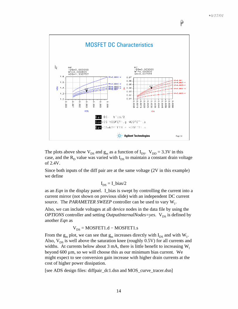
The plots above show VDS and gm as a function of IDS. VDD = 3.3V in this case, and the RD value was varied with IDS to maintain a constant drain voltage of 2.4V.
Since both inputs of the diff pair are at the same voltage (2V in this example) we define
IDS = I_bias/2
as an Eqn in the display panel. I_bias is swept by controlling the current into a current mirror (not shown on previous slide) with an independent DC current source. The PARAMETER SWEEP controller can be used to vary W1.
Also, we can include voltages at all device nodes in the data file by using the OPTIONS controller and setting OutputInternalNodes=yes. VDS is defined by another Eqn as
VDS = MOSFET1.d − MOSFET1.s
From the gm plot, we can see that gm increases directly with IDS and with W1. Also, VDS is well above the saturation knee (roughly 0.5V) for all currents and widths. At currents below about 3 mA, there is little benefit to increasing W1beyond 600 µm, so we will choose this as our minimum bias current. We might expect to see conversion gain increase with higher drain currents at the cost of higher power dissipation.
[see ADS design files: diffpair_dc1.dsn and MOS_curve_tracer.dsn]

15
H•4/17/01
Page 15
Linearity of signal path
• RS is varied from 1 to 101 ohms
VDD
RS RS
RL RL
VrefVin
1
101
NOTE: VDin = Vin - Vref
VDout
Now we will focus on the linearity of the signal path (RF to IF). A transfer characteristic is simulated by sweeping the DC input voltage
VDin = Vin - Vref.
Vref = 2.0V. We would expect that by increasing the resistance RS, adding negative feedback, we would linearize the transfer characteristic by exchanging gain for linearity. In the simulation shown, RS values are stepped using a PARAMETER SWEEP controller from 1 to 101 ohms. We see that the gain (slope) becomes more linear over a wider input voltage range with increasing RS.
Exercise. Evaluate how the choice of Vref affects the transfer characteristic.
[See ADS design file: diffpair_tc.dsn]

16
H•4/17/01
Page 16
Linearity of signal path
VDD
RS RS
RL RL
Vref
Vin
RS = 1
RS = 101
Incremental gain vs. input offset voltage:AC simulation: sweep Vin and Rs
NOTE: Vref = 2 volts
Another way of viewing the linearity of the amplifier is by doing an AC analysis of incremental voltage gain as a function of frequency with RS as a parameter. The plot above illustrates that increasing RS decreases gain but also reduces the relative gain variation with input offset voltage, Vin. In fact, this is the conventional first order treatment for improving linearity of a differential stage, albeit at the expense of gain and noise. But, because the mixer distortion will increase as the large signal input voltage increases, this simple technique is valuable. But, we can never get perfectly flat gain with this simple approach.
[Refer to ADS design files: diffpair_tc.dsn and diffpair_tcgain2.dsn]
The assymetry seen on the high input voltage side is due to the input MOSFET dropping out of saturation.
From this analysis, and if conversion gain and noise are not very important for your application, you would think that larger RS would be better: more effective in reducing distortion. It turns out that this design has some peculiar properties in this regard, so watch for this later.
Exercise: 1. Evaluate how the small-signal gain vs. Vin varies with Ibias as a parameter. Compare your result with diffpair_tcgain4.dsn.

17
H•4/17/01
Page 17
Linearization through LS?
•Doesn’t add noise•Less voltage drop
•But, not as good forlinearity
•Also, inductors onSi have low Q, sowould have both RS
and LS.
f = 900 MHz
LS = 1 nH
LS = 7 nH
A popular technique in low voltage RFIC design is to substitute inductors for resistors. This has the advantages that the ideal inductor will not add noise to the circuit, and it reduces the supply voltage requirement for the circuit. The effectiveness of this approach is somewhat frequency dependent. At 900 MHz, the gain degeneration and linearity improvement for reasonable sized inductors is limited. It becomes more effective at higher frequencies.
[See ADS design: diffpair_tcgain5.dds. Try changing the frequency on the display screen and observe how the inductive degeneration varies.]
Also, inductors on Si substrates have low Q, on the order of 2 to 3. For a Q of 2.5, for example, a 5 nH inductor at 900 MHz would have a series resistance of about 10 ohms. Thus, we really are including both resistance and inductance. We will see that this is a good combination for modifying the input match.

18
H•4/17/01
Page 18
Stability of mixer input port
• dB |S11| > 0: unstable. Why?
Zin, S11
Vref
−V
+VZs
We will do an S-parameter simulation of the Gilbert DB mixer to determine the input impedance as a function of RS. The LO switch is biased on, thus the circuit resembles a cascode.
We see that as RS is increased, the magnitude of S11 becomes greater than 1 (>0dB). This means that the real part of the input resistance is negative, a condition desirable for oscillators, not mixers. We also note that this condition gets worse at higher frequencies. Thus, we need to look more closely to find out why this is happening and find a way to guarantee stability.
[Refer to ADS example files: gilmix_sp.dsn and .dds]
19
H•4/17/01
Page 19
Input impedance of mixer
sT
Sgs
in Zj
ZCj
jZω
ωω
ω ++=1
)(
++
gs
T
CjjR
Rωω
ω 1
Zin, S11
Vref
−V
+VZs
Zs ReZin + ImZin
R
L
++ Lj
CjL
gsT ω
ωω
1
C
++−
CjCjC gs
T
ωωωω 11
2
NOTE: ω T is the unity current gain frequency = gm/ Cgs.
Impedance Model: Zin
Zs
Cgs gmVgs
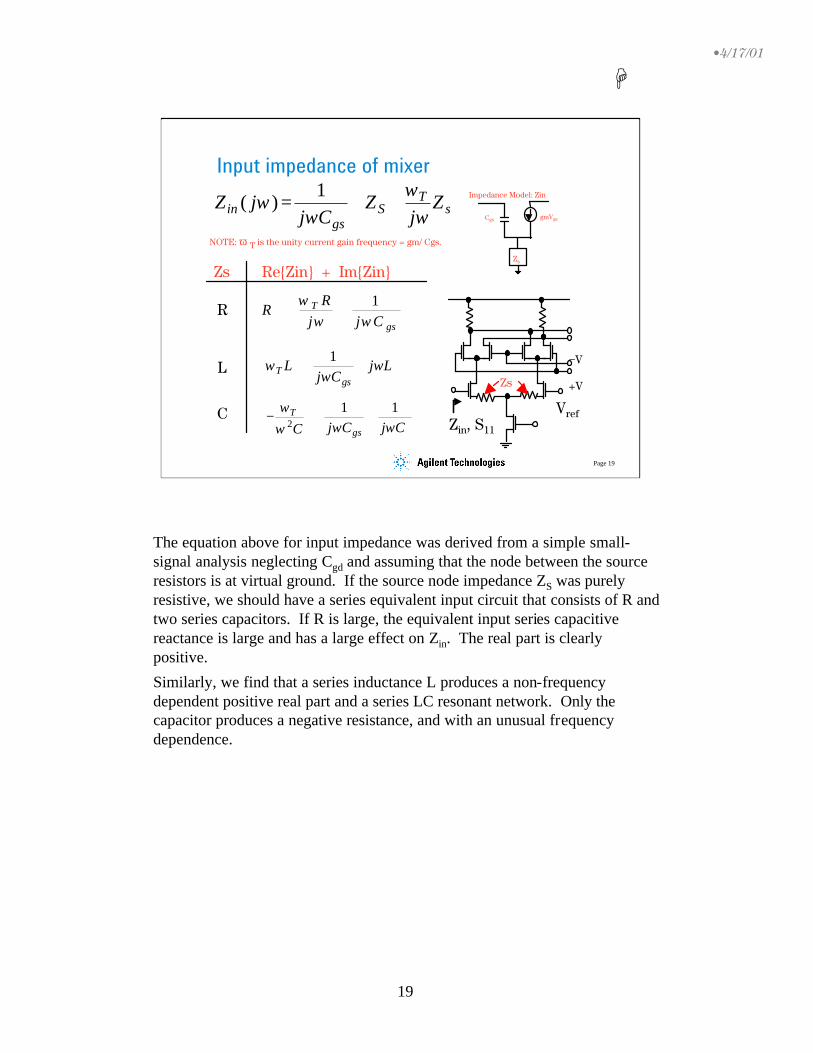
The equation above for input impedance was derived from a simple small-signal analysis neglecting Cgd and assuming that the node between the source resistors is at virtual ground. If the source node impedance ZS was purely resistive, we should have a series equivalent input circuit that consists of R and two series capacitors. If R is large, the equivalent input series capacitivereactance is large and has a large effect on Zin. The real part is clearly positive.
Similarly, we find that a series inductance L produces a non-frequency dependent positive real part and a series LC resonant network. Only the capacitor produces a negative resistance, and with an unusual frequency dependence.

20
H•4/17/01
Page 20
Input impedance of mixer
Vref
−V
+VRs
CSB
2221)1(
ReSBS
SBSTSin
CRCRR
Zω
ω−
−=
Re
Z in
Since we are seeing |S11| > 1, we must have a negative resistance in the input. Why? This is due to the parasitic source to bulk capacitance of the MOSFET. As RS increases, the shunt CSB has greater effect on the source impedance and therefore drives the input impedance negative. If ωTRSCSB > 1, we will have a negative real Zin.
Exercise: Try adding extra shunt capacitance to the source nodes in the schematic gilmix_sp and see how S11 and Zin is affected.
To compensate for the negative resistance, let’s add some series inductance.
21
H•4/17/01
Page 21
Source inductance added
LS = 0
6 nHR
eZ i
n|S
11| d
B
2
4
• Small LS can improve input matchat design frequency of 900 MHz
• It will also help with stability
02
46
RS = 40Ω
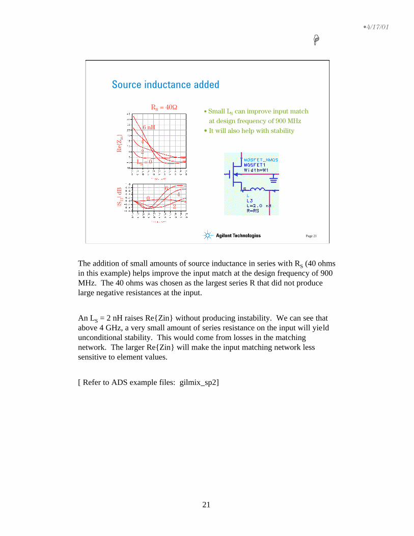
The addition of small amounts of source inductance in series with RS (40 ohms in this example) helps improve the input match at the design frequency of 900 MHz. The 40 ohms was chosen as the largest series R that did not produce large negative resistances at the input.
An LS = 2 nH raises ReZin without producing instability. We can see that above 4 GHz, a very small amount of series resistance on the input will yield unconditional stability. This would come from losses in the matching network. The larger ReZin will make the input matching network less sensitive to element values.
[ Refer to ADS example files: gilmix_sp2]

22
H•4/17/01
Page 22
Zin with added source inductance
•Input impedance varies with RS.
•Since we will evaluate the effect ofRS on distortion, we must designa matching network for each RS
value selected.
10Ω
40Ω
LS = 2 nHR
eZ i
n
We now see that the additional inductance has eliminated the negative real part to the input impedance for RS ≤ 40Ω.
But, RS has a major effect on Zin. Since we saw earlier that RS may influence the linearity of the diff pair, we will want to investigate the dependence of distortion on RS. Thus, we will need to design a matching network for each RSvalue.

23
H•4/17/01
Page 23
Add input matching network
• Off chip - inductances are too large for on-chip fabrication• Calculate components for each RS value to be evaluated• Add single frequency generator for harmonic balance simulation
NOTE: Other side is terminated with Vref_RF.
We have seen that Zin will vary with RS and LS. For LS = 2 nH, we will design a T-network to match the 50 ohm off-chip generator to the mixer input for 3 values of RS. (We will want to investigate the dependence of intermodulation on RS in a later slide.)
RS (Ω) Zin (Ω) L1 C1 L210 29.4-j183 48nH 3.1pF 19.5nH
20 20.8-j200 46.4 4.1 15.7
40 9,4-j221 44.1 7.4 8.3

24
H•4/17/01
Page 24
Use Harmonic Balance simulation
•Highest order of IM products•Fundamental Frequencies:
put highest power source first•Number of harmonics of sources [1] & [2]•Sweep P_RF in 1 dB steps from -30 dBm•Pass drain resistance to data set
Adding the input matching network shown on the previous slide for RS = 10Ωand LS = 2 nH, we can now calculate the conversion gain as a function of whatever parameters we wish to vary. In this example, the RF input power, P_RF, will be swept.
Harmonic balance is the method of choice for simulation of mixers. By specifying the number of harmonics to be considered for the LO and RF input frequencies and the maximum order (highest order of sums and differences) to be retained, you get the frequency domain result of the mixer at all relevant frequencies. To get this information using SPICE or other time domain simulators would require a very long simulation time since at least two complete periods of the lowest frequency component must be generated in order to get accurate FFT results. In addition, the time step must be compatible with the highest frequency component to be considered.
Maximum order corresponds to the highest order IM product (n + m) to be considered (nf[1] ± mf[2]). The simulation will run faster with lower order and fewer harmonics of the sources, but may be less accurate. You should test this by checking if the result changes significantly as you increase order or harmonics.
The frequency with the highest power level (the LO) is always the first frequency to be designated in the harmonic balance controller. Other inputs follow sequencing from highest to lowest power.

25
H•4/17/01
Page 25
LO switch
to diff pairdiff to SE outputconversion
Differential LO source
Differential LO drive is required if you need good LO to IF and LO to RF isolation. This is probably the case, otherwise you could get by with a simpler single-balanced design. Since the LO and RF frequencies are rather close together (in this example), you can’t depend on the input matching network to attenuate the LO signal very much. The LO driver might typically be located on-chip as another diff amp, but to simplify the simulation, it is represented here as two voltage sources at 0 and 180 degrees phase with amplitude VLO. A DC offset of Vref_LO is also needed to correctly bias the LO inputs. We will sweep VLO later to determine the LO amplitude for best IMDperformance.
A differential output is also required in order to obtain the double-balanced properties. Your LO signal, which is common-mode for differential and thus cancels, will show up at full amplitude in the output if single-ended. For the simulation, we can use an ideal voltage-controlled-voltage-source to provide this conversion:
Vout = Vout1 - Vout2
On-chip, we would use another diff amp for this purpose or off-chip, a transformer or balun.
[Refer to gilmix_GC3 for this example]

26
H•4/17/01
Page 26
Gain Compression: P1dB
Equations are added to the display panel which select the IF frequency, calculate the differential IF output power, convert it to dBm, then subtract the RF input power, also in dBm.
conv_gain = dBm(V_IFout2/(2*RD)) − P_RF
V_IFout is the differential output voltage at the IF output frequency. This frequency is selected from the data set using the mix function. Thedownconverted IF at 45 MHz is selected with:
V_IFout = mix(Vout,-1,1).
The indices in the curly brackets are ordered according to fundamental frequencies. Thus, -1,1 selects RF_freq − LO_freq.
Here we can identify the 1 dB gain compression power to be about −12 dBm.
[Refer to ADS example gilmix_GC3]

27
H•4/17/01
Page 27
Exercise...
• OK, now its your turn to run a simulation. Modify the schematic file gilmix_hbGC3 to simulate how P1dB varies as a function of LO voltage.
• To do this, add a PARAMETER SWEEP controller
• The LO voltage range from 0.05 to 0.25V amplitude will be of interest.

28
H•4/17/01
Page 28
IMD simulation
• Use a two-tone generator at themixer input.
• The two input frequencies are separated by F_spacing and each have an input power of P_RF dBm.
• A DC offset Vdc is needed to properlybias the RF input.
We will be mainly concerned with the third-order IMD. This is especially troublesome since it can occur at frequencies within the IF bandwidth. For example, suppose we have 2 input frequencies at 899.990 and 900.010 MHz. Third order products at 2f1 - f2 and 2f2 - f1 will be generated at 899.980 and 900.020 MHz. These may fall within the filter bandwidth of the IF filter and thus cause interference to a desired signal.
Other odd-order products will also be of interest, but may be less reliably predicted unless the device model is precise enough to give accurate nonlinearity in the transfer characteristics up to the 2n-1th order.
[Refer to ADS file gilmix_hbTOI3]
29
H•4/17/01
Page 29
IF output spectrum
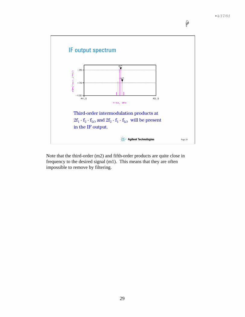
Third-order intermodulation products at 2f1 - f2 - fLO and 2f2 - f1 - fLO will be present in the IF output.
Note that the third-order (m2) and fifth-order products are quite close in frequency to the desired signal (m1). This means that they are often impossible to remove by filtering.

30
H•4/17/01
Page 30
Third-order intercept definition
IIP3
OIP3
slope = 3
slope = 1
A widely-used figure of merit for IMD is the third-order intercept (TOI) point. This is a fictitious signal level at which the fundamental and third-order product terms would intersect. In reality, the intercept power is 10 to 15 dBm higher than the P1dB gain compression power, so the circuit does not amplify or operate correctly at the IIP3 input level. The higher the TOI, the better the large signal capability of the mixer.
It is common practice to extrapolate or calculate the intercept point from data taken at least 10 dBm below P1dB. One should check the slopes to verify that the data obeys the expected slope = 1 or slope = 3 behavior. When this is true,
OIP3 = (PIF − PIMD)/2 + PIF.Also, the input and output intercepts are simply related by the gain:
OIP3 = IIP3 + conversion gain.
In the data display above, equations are used to select out the IF fundamental tone and the IMD tone, in this case, the upper sideband. The mix function now has 3 indices since there are 3 frequencies present: LO, RF1 and RF2. The dBm conversion again takes into account the actual differential output load resistance.
The two IMD sidebands should be approximately of equal power if the simulation is correct. If not, increase the order of the LO in the HB controller and see if this makes the sidebands more symmetric.

31
H•4/17/01
Page 31
IP3 dependence on LO voltage
gain
IIP3
OIP3
Now we can begin to investigate the third-order intercept (TOI) sensitivity to various design parameters. The LO voltage (amplitude) dependence is shown above. Clearly, it is beneficial to provide sufficient LO voltage to fully switch the upper transistors. The larger voltage decreases the distortion by increasing the slew rate at the switch input. The switch thus spends less time in a nonlinear intermediate state. We reach a point of diminishing returns somewhere around 0.15 to 0.20 V in this case. IIP3 is actually declining because the conversion gain is increasing with VLO. It takes less input power to obtain the output intercept power when gain is higher.
[Refer to ADS file gilmix_hbTOI3]

32
H•4/17/01
Page 32
TOI dependence on RS
RS Gain OIP3 IIP3 Vgate
10 ohms 12.9 dB 7.1 dBm -5.8 dBm 0.048V
20 13.1 6.0 -7.1 0.061
40 14.3 3.1 -11.2 0.098
OIP gets worse with RS
Remember our earlier simulations of diffamp gain and linearity vs. RS? We found improvement in the linearity and reduced gain as the source resistance was increased. In fact, this is a standard method for linearizing diffamps! Why isn’t it working here? We see quite the opposite trend.
When the input impedance was simulated, we found rapid variation with RS. A different input matching network is needed for each RS value to provide a conjugate match and maximum transducer gain. As RS increases, ReZin gets smaller, and the voltage on the gate for a given input power increases. We also find the conversion gain increasing. It is this passive gain in the input matching network that is degrading the TOI properties of the mixer. The RF voltage increases more rapidly with RS than the inherent gain of the amplifier itself decreases due to feedback.
33
H•4/17/01
Page 33
P1dB & TOI dependence on RD
400Ω
100Ω
200Ω
300Ωgain
OIP3
IIP3
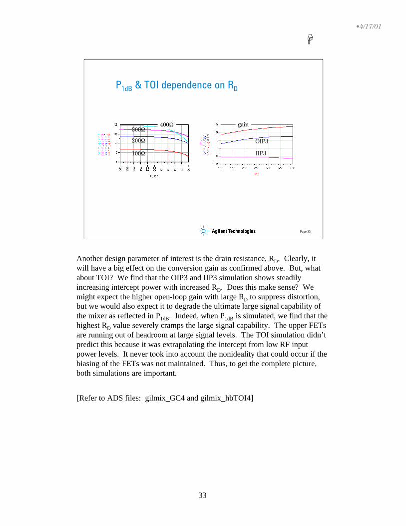
Another design parameter of interest is the drain resistance, RD. Clearly, it will have a big effect on the conversion gain as confirmed above. But, what about TOI? We find that the OIP3 and IIP3 simulation shows steadily increasing intercept power with increased RD. Does this make sense? We might expect the higher open-loop gain with large RD to suppress distortion, but we would also expect it to degrade the ultimate large signal capability of the mixer as reflected in P1dB. Indeed, when P1dB is simulated, we find that the highest RD value severely cramps the large signal capability. The upper FETs are running out of headroom at large signal levels. The TOI simulation didn’t predict this because it was extrapolating the intercept from low RF input power levels. It never took into account the nonideality that could occur if the biasing of the FETs was not maintained. Thus, to get the complete picture, both simulations are important.
[Refer to ADS files: gilmix_GC4 and gilmix_hbTOI4]

34
H•4/17/01
Page 34
Exercise
• Using the ADS files as templates, simulate the TOI and gain compression of the mixer while varying:
• VDD
• I_bias
• Note: when you vary I_bias, you should keep the drain voltage constant by varying the RD value. This can be done by defining RD(I_bias) with VarEqn statement in the schematic window. See how much you can improve TOI with larger bias current.
You can check your answers with files gilmix_hbTOI5 and gilmix_hbTOI7

35
H•4/17/01
Page 35
Isolation between ports
• The mixer is not perfectly unilateral -
leakage between:
• LO to IF
• LO to RF
• RF to IF
• Determine the magnitude of these leakage components at the IF and RF ports using the mix function to select frequencies.
Isolation can be quite important for certain mixer applications. For example, LO to RF leakage can be quite serious in direct conversion receiver architectures because it will remix with the RF and produce a DC offset. Large LO to IF leakage can degrade the performance of a mixer postamp.

36
H•4/17/01
Page 36
Isolation between ports
UNREALISTIC !
The excellent isolation between ports on double balanced mixers depends on precise balance. The simulation is using ideal components that are perfectly matched and gives grossly optimistic estimates of LO2RF and RF2IF isolation. In real implementations, the MOSFETs and resistors may have slight variations in their parameters that could unbalance the mixer enough to degrade performance.

37
H•4/17/01
Page 37
Isolation with imbalance
• Imbalance in RD is added: RD ± ∆RD
• VLO = 0.20V
The drain resistors are intentionally skewed by an offset resistance ∆RD to illustrate the sensitivity of LO2RF and RF2IF isolation to imbalance. The predictions become more realistic.
[See ADS file gilmix_iso]
38
H•4/17/01
Page 38
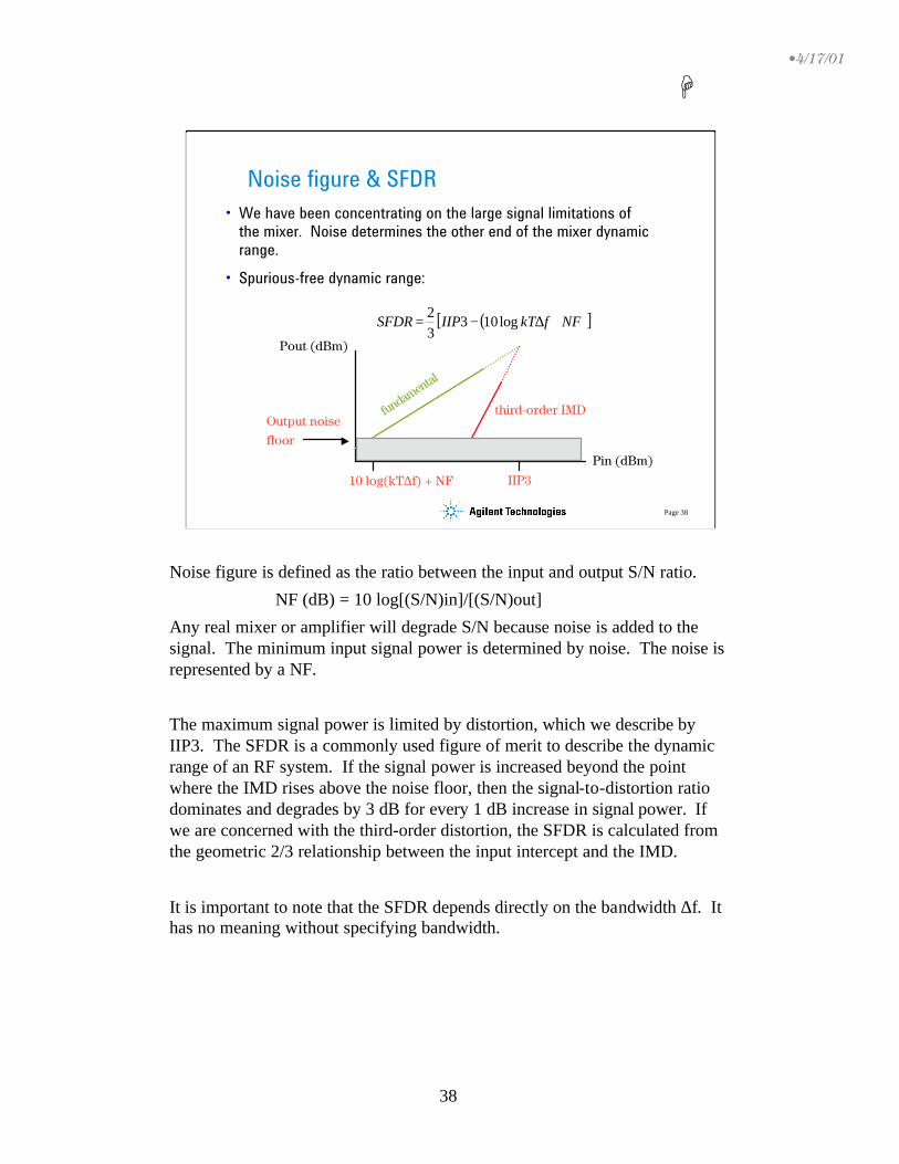
Noise figure & SFDR• We have been concentrating on the large signal limitations of
the mixer. Noise determines the other end of the mixer dynamic range.
• Spurious-free dynamic range:
Output noisefloor
Pout (dBm)
10 log(kT∆f) + NF IIP3Pin (dBm)
fundamental
third-order IMD
( )[ ]NFfkTIIPSFDR +∆−= log10332
Noise figure is defined as the ratio between the input and output S/N ratio.
NF (dB) = 10 log[(S/N)in]/[(S/N)out]
Any real mixer or amplifier will degrade S/N because noise is added to the signal. The minimum input signal power is determined by noise. The noise is represented by a NF.
The maximum signal power is limited by distortion, which we describe by IIP3. The SFDR is a commonly used figure of merit to describe the dynamic range of an RF system. If the signal power is increased beyond the point where the IMD rises above the noise floor, then the signal-to-distortion ratio dominates and degrades by 3 dB for every 1 dB increase in signal power. If we are concerned with the third-order distortion, the SFDR is calculated from the geometric 2/3 relationship between the input intercept and the IMD.
It is important to note that the SFDR depends directly on the bandwidth ∆f. It has no meaning without specifying bandwidth.

39
H•4/17/01
Page 39
Determining Noise Figure
• Use harmonic balance simulator for mixer NF.
• takes into account any nonlinearities and harmonics that could mix noise down into the IF band.
• If P_RF << P_ LO, either a 1-tone generator or a passive termination can be used at the input with equal accuracy.
• Noise Figure is calculated.
• Ideal filter (centered on RF) is added in simulation.
• Noise contributions within mixer added.
• NF = 5.7 dB.
• SFDR = 112 dB (with 100 kHz BW).
The harmonic balance simulator will take into account wideband noise that is generated in the mixer. Some of this noise gets mixed down to the IF frequency from the harmonics of the LO. If the RF signal is of small amplitude, the harmonics that it might generate can be neglected, and either a 1-tone generator or a passive termination can be used. The predictions will be the same.

40
H•4/17/01
Page 40
Final mixer specs
• IIP3 = - 6 dBm
• P1dB = - 12 dBm
• Conversion gain = 13 dB
• NF = 5.7 dB
• SFDR = 112 dB (100 kHz BW)
• Power dissipation = 20 mW
Here are the final mixer performance specifications that have resulted from this example. We have clearly not exhausted the design space, and there are many other factors that could be considered that might have further influence on the results.
In the next slide, there is a list of other circuits that we should also include if time permitted.

41
H•4/17/01
Page 41
What’s next?
• We would also need to design:
• LO buffer for single-ended to differential
• IF buffer for differential to single-ended
• biasing for the RF and LO inputs

42
H•4/17/01
Page 42
Conclusion
• Understand operation of MOSFET Gilbert mixer
• Biasing considerations
• Design for stability, linearity and noise
• Specify performance: NF, P1dB, TOI, SFDR
• Now, go through the ADS example files, modify them for your application. Use them as templates for your own design work.
Learning objectives:
Further resources:

43
H•4/17/01
Page 43
References
• [1] Gray, P. R. and Meyer, R. G., Design of Analog Integrated Circuits, 3rd Ed., Chap. 10, Wiley, 1993.
• [2] Gilbert, B., “Design Considerations for BJT Active Mixers”, Analog Devices, 1995.
• [3] Lee, T. H., The Design of CMOS Radio-Frequency Integrated Circuits, Chap. 11, Cambridge U. Press, 1998.
References
[1] Gray, P. R. and Meyer, R. G., Design of Analog Integrated Circuits, 3rd Ed., Chap. 10, Wiley, 1993.
[2] Gilbert, B., “Design Considerations for BJT Active Mixers”,Analog Devices, 1995.
[3] Lee, T. H., The Design of CMOS Radio-Frequency Integrated Circuits, Chap. 11, Cambridge U. Press, 1998.

44
H•4/17/01
Page 44
End of Design Seminar...

www.agilent.com/fi nd/emailupdatesGet the latest information on the products and applications you select.
www.agilent.com/fi nd/agilentdirectQuickly choose and use your test equipment solutions with confi dence.
Agilent Email Updates
Agilent Direct
www.agilent.comFor more information on Agilent Technologies’ products, applications or services, please contact your local Agilent office. The complete list is available at:www.agilent.com/fi nd/contactus
AmericasCanada (877) 894-4414 Latin America 305 269 7500United States (800) 829-4444
Asia Pacifi cAustralia 1 800 629 485China 800 810 0189Hong Kong 800 938 693India 1 800 112 929Japan 0120 (421) 345Korea 080 769 0800Malaysia 1 800 888 848Singapore 1 800 375 8100Taiwan 0800 047 866Thailand 1 800 226 008
Europe & Middle EastAustria 0820 87 44 11Belgium 32 (0) 2 404 93 40 Denmark 45 70 13 15 15Finland 358 (0) 10 855 2100France 0825 010 700* *0.125 €/minuteGermany 01805 24 6333** **0.14 €/minuteIreland 1890 924 204Israel 972-3-9288-504/544Italy 39 02 92 60 8484Netherlands 31 (0) 20 547 2111Spain 34 (91) 631 3300Sweden 0200-88 22 55Switzerland 0800 80 53 53United Kingdom 44 (0) 118 9276201Other European Countries: www.agilent.com/fi nd/contactusRevised: March 27, 2008
Product specifi cations and descriptions in this document subject to change without notice.
© Agilent Technologies, Inc. 2008
For more information about Agilent EEsof EDA, visit:
www.agilent.com/fi nd/eesof
nstewart
Text Box
Printed in USA, April 17, 2001 5989-9103EN