
Présent et futur de la spintronique LAAS, 17/12/ 08 TMR, etc … Spintronics. Spin ... Other...
51
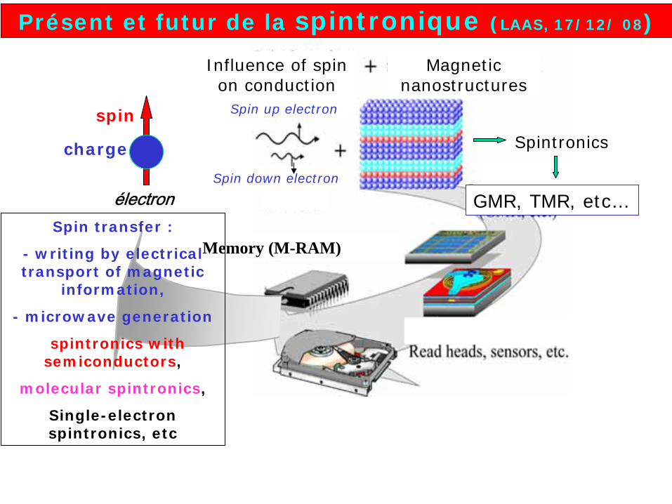
Influence of spin on conduction Magnetic nanostructures Memory (M-RAM) GMR, TMR, etc… Spintronics Spin up electron Spin down electron Spin transfer : - writing by electrical transport of magnetic information, - microwave generation spintronics with semiconductors, molecular spintronics, Single-electron spintronics, etc Présent et futur de la spintronique (LAAS, 17/12/ 08) spin charge électron
-
Upload
truongcong -
Category
Documents
-
view
214 -
download
0
Transcript of Présent et futur de la spintronique LAAS, 17/12/ 08 TMR, etc … Spintronics. Spin ... Other...
Influence of spin on conduction
Magnetic nanostructures
Memory (M-RAM)
GMR, TMR, etc…
Spintronics
Spin up electron
Spin down electron
Spin transfer :
- writing by electrical transport of magnetic
information,
- microwave generation
spintronics with semiconductors,
molecular spintronics,
Single-electron spintronics, etc
Présent et futur de la spintronique (LAAS, 17/12/ 08)
spin
charge
électron

Introduction :
Spin dependent conduction in
ferromagnetic conductors,
Giant Magnetoresistance (GMR),
Tunnel Magnetoresistance (TMR)

E
EF
n (E)
n (E)
Spin dependent conduction in ferromagnetic metals (two current model)
Mott, Proc.Roy.Soc A153, 1936
Fert et al, PRL 21, 1190, 1968
Loegel-Gautier, JPCS 32, 1971
Fert et al,J.Phys.F6, 849, 1976
Dorlejin et al, ibid F7, 23, 1977ρ
ρ
I
I α= ρ↓
/ ρ↑
or β
= (ρ↓
-
ρ↑
)/ (ρ↓
+ ρ↑
) = (α
- 1)/(α
+ 1)
E
EF
n (E)
n (E)
Ni d bandCr d↑
level
Virtual boundstate
Cr d↓
level
Ni d band
α ≈ 0.3
α ≈ 20
Ti V Cr Mn Fe Co Ni
ρ↓
ρ↑
α= ρ↓
/ ρ↑

Mixing
impurities
A and B with
opposite or similar
spin asymmetries: the pre-concept of GMR
Example: Ni + impurities A and B (Fert-Campbell, 1968, 1971)
1st case 2d case αA > 1, αB < 1 αA and αB > 1
High mobility channel low ρ
ρAB >> ρA + ρB ρAB ≈ ρA + ρB
spin
spin
spin
spin
J. de Physique 32, 1971
α
= ρ↓
/ρ↑

Fe
Fe
Cr
Cr
• Magnetic multilayers
Fe

Fe
Fe
Cr
Cr
Magnetizations of Fe layers at zero fieldin Fe/Cr multilayers
• Magnetic multilayers
Fe
P. Grünberg, 1986 →
antiferromagnetic interlayer coupling

Fe
Fe
Cr
Cr
Magnetizations of Fe layers in an
applied fieldin Fe/Cr multilayers
• Magnetic multilayers
Fe
H
P. Grünberg, 1986 →
antiferromagnetic interlayer coupling

~ + 80%
• Giant Magnetoresistance (GMR)(Orsay, 1988, Fe/Cr multilayers, Jülich, 1989, Fe/Cr/Fe trilayers)
Resistance ratio
Magnetic field (kGauss)
AP (AntiParallel) P (Parallel)Current
V=RI
Orsay Jülich

~ + 80%
• Giant Magnetoresistance (GMR)(Orsay, 1988, Fe/Cr multilayers, Jülich, 1989, Fe/Cr/Fe trilayers)
Resistance ratio
Magnetic field (kGauss)
Anti-parallel magnetizations (zero field, high resistance)
CrFe
Fe
Parallel magnetizations (appl. field, low resist.)
CrFe
Fe
Condition for GMR: layer thickness ≈
nm
AP (AntiParallel) P (Parallel)Current
net current

track
Read head of hard disc drive
GMR sensor5 nm
Magnetic
fields generated
by the media
0
1997 (before GMR) : 1 Gbit/in2 , 2007 : GMR heads ~ 600 Gbit/in2
voltage
current
Recent review : « The emergence of spintronics in data storage »
Chappert, AF et al Nat. Mat.(Nov.07)

STT-RAM (in demonstration)
with MgO tunnel junctions
+ writing by spin transfer
Applications: - read heads of Hard Disc Drive
- M-RAM (Magnetic Random Access Memory) and STT-RAM
~ 100 nm
• Magnetic Tunnel Junctions,Tunneling
Magnetoresistance
(TMR)
Low resistance state High resistance state
ferromagneticelectrodes
tunnelingbarrier
(insulator) APP
Moodera
et al, 1995, Miyasaki
et al,1995,
CoFe/Al2
O3
/Co, MR ≈30-40%
Jullière, 1975, low T, hardly reproducible
≈
0.1 μm
CoFeB/MgO/CoFeB, ΔR/R
≈
500% at
RT in 2006-2007
aims: density/speed of DRAM/SRAM + nonvolatilty
+ low
energy
consumption
MRAM (2006, Freescale)

First examples
on Fe/MgO/Fe(001): CNRS/Thales (Bowen, AF et al, APL2001)
Nancy (Faure-Vincent et al, APL 2003) Tsukuba
(Yuasa
et al, Nature Mat. 2005)
IBM (Parkin
et al, Nature Mat. 2005) ….etc
Epitaxial magnetic tunnel junctions (MgO, etc)
Yuasa et al, Fe/MgO/Fe Nature Mat. 2005
ΔR/R = (RAP
-RP
)/ RP ≈
200% at
RT
CoFeB/MgO/CoFeB,
ΔR/R ≈
500% at
RT in several laboratories
in 2006-2007
Clearer picture of the physics of TMR:
what is inside the word « spin polarization »?
+2006-2007

Mathon and Umerski, PR B 1999 Mavropoulos et al, PRL 2000 Butler et al , PR B 2001 Zhang and Butler, PR B 2004 [bcc Co/MgO/bcc Co(001)]
P
AP Δ1
Δ2’
Δ1
Δ5
Δ5Δ2’
Tunneling from to
spin ↑
state (majority spin) of symmetry Δ1
at EF
spin ↑
state (majority spin) of symmetry Δ1
at EF
P
spin ↑
state (majority spin) of symmetry Δ1
at EF
With reversed M in the right electrode,
spin ↑ corresponds to a
minority spin band state without Δ1 character at E F
in which the tunneling Δ1 el.
cannot be accomodated
AP

Common physics:
spin accumulation
spins injected to long distances
by diffusion
Spin Transfer (magnetic switching, microwave generation)
Spintronics with semiconductors
Spintronics with molecules

0
2
4
6
8
10
0 100 200 300 400 500
Co thickness (nm)M
R ra
tio (%
)
400 nm
Co/Cu: Current ⊥ to Plane (CPP) -GMR of multilayered nanowires (L.Piraux, AF et al, APL 1994,JMMM 1999)
CIP-GMR
scaling length = mean free path
CPP-GMR
scaling length = spin diffusion length >> mean free path
spin accumulation theory (Valet-Fert, PR B 1993)
100 nm
Other results: MSU group, PRL 1991, JMMM 1999
CPP-GMR subsists at almost 1μm

F Ms fl = spin diffusion length
in FM
= spin diffusion length
in NMN Ms fl
Spin injection/extraction at a NM/FM interface (beyond ballistic range)
NM FM
zone of spin accumulation
NMsfl FM
sfl
EF↑
EF↑
= spin↑
chemical potential
Spin accumulation Δμ= EF↑
-EF↓
Spin current = J↑
-J↓
z
z
EF↑
-EF↓
~ exp(z/ ) in FMF Ms fl
EF↑
-EF↓
~ exp(-z/ ) in NMN Ms fl
N Ms fl FM
sfl
EF↓
= spin↓
chemical potential
E
J↑
-J↓
J↑
+J↓
= current spin polarization
(illustration in the simplest case = flat band, low current,
no interface resistance, single polarity)
(example: 0.5 μm in Cu, >10μm in carbon
nanotube)

F Ms fl = spin diffusion length
in FM
= spin diffusion length
in NMN Ms fl
Spin injection/extraction at a NM/FM interface (beyond ballistic range)
NM FM
zone of spin accumulation
NMsfl FM
sfl
EF↑
EF↑
Spin accumulation Δμ= EF↑
-EF↓
Spin current = J↑
-J↓
z
z
N Ms fl FM
sfl
EF↓
E
(illustration in the simplest case = flat band, low current,
no interface resistance, single polarity)
Description*
: Boltzmann-type formalism
with the distribution function associated
to a spin
and position dependent
chemical pot. which leads
to
macroscopic equations**
relating the
charge and spin currents to a
spin dependent
electro-chemical potential
μσ
(z)= eV(z) + EFσ
(z)
CPP-GMR: multi-interface with interface resistances. Semiconductors: new problems with band bending, large currents, “conductivity mism.” Spin torque: non-colinear situation
*Valet and Fert, PR B 48, 7099, 1993.
** similar equ. in Silsbee-Johnson and van Son et al
)(zEFσ

NM
= metal
or semiconductor
FM
zone of spin accumulation
NMsfl FM
sfl
EF↑
EF↑
Spin accumulation Δμ= EF↑
-EF↓
Spin current = J↑
-J↓
z
z
N Ms fl FM
sfl
EF↓
E
NM= metal
Semiconductor/ F metal
If similar
spin spliting
on both
sides
but much
larger
density
of states in F metal
much
larger
spin accumulation density
and much
more spin flips
on magnetic
metal
side
almost
complete
depolarization
of
the current
before
it
enters
the SCNM = semiconductor
1) situation without interface resistance
(« conductivity mismatch »)
(Schmidt et al, PR B 2000)
Spin injection/extraction at a Semiconductor/FM interface

NM
= semiconductor
EF↑
Rasbah, PR B 2000 A.F-Jaffrès, PR B 2001
Spin accumulation Δμ= EF↑
-EF↓
N Msfl FM
sflz
EF↑
Current Spin Polarization
(J↑
-J↓
)/(J↑
+J↓
)
FM spin dependent. interf. resist. (ex:tunnel barrier)
EF↓
EF↑
Spin dependent drop of the electro-chemical potential
Discontinuity increases the spin accumulation in NM
re-balanced spin relaxations in F and NM
extension of the spin- polarized current into the
semiconductor
e-
NsfNNb lrr ρ=≈*
NsfNNb lrr ρ=>>*
Spin injection/extraction at a Semiconductor/FM interface

J↑
-J↓
J↑
+J↓*
*
bNF
bFrrr
rr++
+=
γβDeviations from at large current density (drift effect)
= low current limit
current density
= deviations
from the low
current
limit
(nondegenerate semiconductor)
from Jaffrès and A.F.
(see also Yu and Flatté)

(tranport of magnetization by an electrical curent)
- fundamentals
-
switching of magnetization by spin transfer and applications (STT-RAM, reprogrammable devices)
- microwave oscillations by spin transfer and applications to telecommunications.s
-
Spin transfer

Spin transfer(J. Slonczewski, JMMM 1996, L. Berger, PR B 1996)
S
S≡
Torque on S ≈
Mx(MxM0 )
Ex:Cobalt/Copper/ Cobalt
The transverse component of the spin current is absorbed and transferred
to the total spin of the layer
∝
j M x (M x M0
)

Au
4 nm10 nm
Free magn. layer Cu
Polarizer
Trilayered pillar or tunnel junction
Au
CoFeBMgO
CoFeB
Tunnel junction ≈
50x170 nm²
70 nm
Metallic pillar ≈
50x150 nm²

Au
4 nm10 nm
Free magn. layer Cu
Polarizer
Trilayered pillar or tunnel junction
Metallic pillar ≈
50x150 nm²
x
1) Magnetization switching by spin transfer
2) Sustained precession of the magnetization of the free layer
and generation of radio- frequency oscillations
Two regimes of spin transfer
Applications: writing a memory, etc
Applications: spin transfer nano- oscillators (NSTOs) for
communications (telephone, radio, radar)
Zero or low field
Appl. field
H
Polarizer magnetization
Free layer magnetization
70 nm
Tunnel junction ≈
50x170 nm²
Au
CoFeBMgO
CoFeB

Regime of irreversible magnetic switching
AP
P
H=7 Oe RT
typical switching current ≈
107A/cm2
switching time can be as short as 0.1 ns (Chappert et al)
-2 014,4
14,5
14,6
dV/d
I (Ω
)
I (m A)
-1.0x10⁵ -5.0x10⁴ 0.0 5.0x10⁴ 1.0x10⁵
400000
450000
500000
550000
Res
ista
nce
(Ω)
Current density (A.cm-2 )
30 K
1 x 10⁵ A/cm2
Py/Cu/Py 50nmX150nm (Boulle, AF et al) GaMnAs/InGaAs/GaMnAs tunnel junction (MR=150%)
(Elsen, AF et al, PR B 2006)
First experiments
on pillars:
Cornell
(Katine
et al, PRL 2000)
CNRS/Thales (Grollier
et al, APL 2001)
IBM (Sun et al, APL 2002) -1.0
-0.50.0
0.51.0
-0.1
0.0
0.1
-1.0-0.5
0.00.5
1.0
Mz
M yMx
APP
m
Py = permalloy
Au
4 nm10 nm
Free magn. layer
Polarizer
Cu

Regime of steady precession (microwave frequency range)
CNRS/Thales, Py/Cu/Py
(Py
= permalloy)
Polarizer magnetization
-1.0-0.5
0.00.5
1.0
-0.5
0.0
0.5
-1.0
-0.5
0.0
0.51.0
mH
Mz
M y
Mx
-1.0-0.5
0.00.5
1.0
-0.5
0.0
0.5
-1.0
-0.5
0.00.5
1.0mH
Mz
M y
Mx
Increasing current
3,5 4,00
1
2
3
Pow
er (p
W/G
Hz)
Frequency (GHz)Microwave power spectrum of the
oscillations of a permalloy-based pillar
-4 014,4
15,0
15,6
dV/d
I (Ω
)
I (mA)
5600G
9G
applied field

Regime of steady precession for tunnel junctions
CoFeB/MgO/CoFeB junction (J.Grollier, AF et al 2008, collaboration S. Yuasa et al, AIST)
4.5 5.0 5.50
30
60
90
PS
D (n
W/G
Hz)
Frequency (GHz)
1.40mALorentzian fit
H = -303G
PSDmax = 90 nW/GHz
width=62MHZ
RT
Tunnel junction ≈
50x170 nm²
Au
CoFeBMgO
CoFeB
Spin Transfer mixes very different (and interacting) problems:
transport (in metallic pillars, tunnel junctions, point contacts)
problems of non-linear dynamics
micromagnetism (non-uniform excitations, vortex motion..)

Au Py (8nm, free)Cu ( 8nm)
Co (8nm, fixed)IrMn (15nm) or CoO or Cu
100x170nm²
Co/Cu/Py (« wavy » angular variation calculated
by
Barnas, AF et al, PR B 2005)
-4 014,4
15,0
15,6
dV/d
I (Ω
)
I (mA)
5600G
9G
Negative I (mA)
Py/Cu/Py (standard)
Positive I
Boulle, AF et al, Nature Phys. 2007 oscillations at H=0
free Py:fast spin relaxation
fixed Co: slower spin relaxation
H ≈
0

Current pulse
Applications of magnetic
switching
by spin transferSwitching of reprogrammable devices (example: STT-RAM)
To replace M-RAM (switching by external magnetic field : nonlocal,
risk of « cross-talk » limiting integration, too large currents)
STT-RAM :«Electronic» reversal by spin transfer from an electrical current

Current pulse
CMOS logic
Embedded STT-RAM
Non volatile FPGA Logic Circuits
Flash and SRAM would be replaced by a non volatile memory (<10F2) embedded directly inside the look
up table (Sony, IEEE Proc. 07)
Applications of magnetic
switching
by spin transferSwitching of reprogrammable devices (example: STT-RAM)
To replace M-RAM (switching by external magnetic field : nonlocal,
risk of « cross-talk » limiting integration, too large currents)
STT-RAM :«Electronic» reversal by spin transfer from an electrical current

Spin Transfer Oscillators (STOs)
(telecommunications, radar, chip to chip communication…)
-Needed
improvements
--
Increase
of power by synchronization of a large number N
of STOs
( x N2 )
-Optimization
of the emission linewidth
Advantages:
-direct
oscillation in the microwave
range (0.5-40 GHz)
-agility: control of frequency
by dc
current
amplitude
- high
quality
factor
-
small
size (≈
0.1μm) (on-chip integration, chip to chip com., microwave assisted writiing in HDD)
f/fΔf ≅ 18000

Spintronics with semiconductors
and molecules

GaMnAs (Tc →170K) and R.T. FS
Electrical control of ferromagnetism
TMR, TAMR, spin transfer (GaMnAs)
Field-induced metal/insulator transition
Spintronics with semiconductors
Magnetic metal/semiconductor hybrid structures
Example: spin injection from Fe into LED
(Mostnyi et al, PR. B 68, 2003)
Ferromagnetic semiconductors (FS)
F1 F2Semiconductor
channel
V
Logic devices, spin transistor ?
Semiconductor lateral channel between spin-polarized source and drain
transforming spin information into large(?) and tunable (by gate voltage)
electrical signal

Nonmagnetic lateral channel between spin-polarized source and drain
Semiconductor channel:
« Measured effects of the order of 0.1-1% have been reported for the change in
voltage or resistance (between P and AP)…. », from the review article
« Electrical Spin Injection and Transport in Semiconductors » by BT Jonker
and ME Flatté in Nanomagnetism (ed.: DL Mills and JAC Bland, Elsevier 2006)
Carbon nanotubes:
ΔR/R ≈
60-70%, VAP -VP ≈
20-60 mV
LSMO LSMO
LSMO = La2/3 Sr1/3 O3
MW-CNT 1.5 μm
L.Hueso, N.D. Mathur,A.F. et al, Nature 445, 410, 2007
F1 F2Semiconductor
channel
PAP
M

Nonmagnetic lateral channel between spin-polarized source and drain
Semiconductor channel:
« Measured effects of the order of 0.1-1% have been reported for the change in
voltage or resistance (between P and AP)…. », from the review article
« Electrical Spin Injection and Transport in Semiconductors » by BT Jonker
and ME Flatté in Nanomagnetism (ed.: DL Mills and JAC Bland, Elsevier 2006)
Carbon nanotubes:
ΔR/R ≈
60-70%, VAP -VP ≈
20-60 mV
LSMO LSMO
LSMO = La2/3 Sr1/3 O3
nanotube 1.5 μm
L.Hueso, N.D. Mathur,A.F. et al, Nature 445, 410, 2007
F1 F2Semiconductor
channel
PAP
MR ≈
72%

Nonmagnetic lateral channel between spin-polarized source and drain
Semiconductor channel:
« Measured effects of the order of 0.1-1% have been reported for the change in
voltage or resistance (between P and AP)…. », from the review article
« Electrical Spin Injection and Transport in Semiconductors » by BT Jonker
and ME Flatté in Nanomagnetism (ed.: DL Mills and JAC Bland, Elsevier 2006)
Carbon nanotubes:
ΔR/R ≈
60-70%, VAP -VP ≈
20-60 mV
AP
P PLSMO LSMO
LSMO = La2/3 Sr1/3 O3
nanotube 1.5 μm
L.Hueso, N.D. Mathur,A.F. et al, Nature 445, 410, 2007
F1 F2Semiconductor
channel
PAP
60%

AF and Jaffrès PR B 2001 +cond-mat 0612495, +
IEEE Transactions.on
Electronic Devices.
54,5,921,2007
10-4 10-2 100 102 1040.00
0.05
0.10
0.15
0.20
0.25
0.30
0.35
NlSF=2µm
tN=20nm
tN=2µm
tN=200nm
rb
*/rN
ΔR
/RP
10-4 10-2 100 102 1040.00
0.05
0.10
0.15
0.20
0.25
0.30
0.35
NlSF=2µm
tN=20nm
tN=2µm
tN=200nm
rb
*/rN
ΔR
/RP
sfbn
b
sfnP
rfor
raszerotodrops
RR
ττ
ττγγ
>>∝
+−
=Δ
*
*
22
/1
/1)1/(
Condition
dwell time τn < spin lifetime τsf
Condition for
spin injection
Nb rr /*
vrL
vt
L
timedwell
b
rn
*
*2
∝=τ
ΔR
/RP
1.6
1.2
0.8
0.4
0.0
L=20nmL
L
NsfNN
b
lr
r
ρ
γγ
=
==
∝=
0.8) (calc.withresistance interface theofasymmetry spin
teff1/trans.coresist.interfaceareaunit **r
10-4 10-2 100 102 1040.00
0.05
0.10
0.15
0.20
0.25
0.30
0.35
NlSF=2µm
tN=20nm
tN=2µm
tN=200nm
rb
*/rN
ΔR
/RP
10-4 10-2 100 102 1040.00
0.05
0.10
0.15
0.20
0.25
0.30
0.35
NlSF=2µm
tN=20nm
tN=2µm
tN=200nm
rb
*/rN
ΔR
/RP
Condition
dwell time τn < spin lifetime τsf
Condition for
spin injection
Nb rr /*
F1 F2Semiconductor
channel
V
L
F1 F2Semiconductor
channel
V
L
ΔR
/RP
1.6
1.2
0.8
0.4
0.0
L=20nmL
LInterface resistance rb *
in most experiments
Two interface spin transport
problem (diffusive regime)
sfn ττ >>NsflL / Ll N
sf /
Window only for lsf (N) > L
1)( 2 −∝L
lwindow sf

10-4 10-2 100 102 1040.00
0.05
0.10
0.15
0.20
0.25
0.30
0.35
NlSF=2µm
tN=20nm
tN=2µm
tN=200nm
rb
*/rN
ΔR
/RP
Window only for lsf (N) > L
10-4 10-2 100 102 1040.00
0.05
0.10
0.15
0.20
0.25
0.30
0.35
NlSF=2µm
tN=20nm
tN=2µm
tN=200nm
rb
*/rN
ΔR
/RP
10-4 10-2 100 102 1040.00
0.05
0.10
0.15
0.20
0.25
0.30
0.35
NlSF=2µm
tN=20nm
tN=2µm
tN=200nm
rb
*/rN
ΔR
/RP
Condition
dwell time τn < spin lifetime τsf
Condition for
spin injection
Nb rr /*
ΔR
/RP
1.6
1.2
0.8
0.4
0.0
L=20nmL
L10-4 10-2 100 102 104
0.00
0.05
0.10
0.15
0.20
0.25
0.30
0.35
NlSF=2µm
tN=20nm
tN=2µm
tN=200nm
rb
*/rN
ΔR
/RP
Condition
dwell time τn < spin lifetime τsf
Condition for
spin injection
Nb rr /*
F1 F2Semiconductor
channel
V
L
F1 F2Semiconductor
channel
V
L
1.6
1.2
0.8
0.4
0.0
L=20nmL
L
Two interface spin transport
problem (diffusive regime)
vrL
vt
L
timedwell
b
rn
*
*2
∝=τAF and Jaffrès
PR B 2001* +cond-mat 0612495, +
IEEE Tr.El.Dev*. 54,5,921,2007
*calculation. for Co and GaAs
at RT
NsflL / Ll N
sf /
sfbn
b
sfnP
rfor
raszerotodrops
RR
ττ
ττγγ
>>∝
+−
=Δ
*
*
22
/1
/1)1/(
Min, Motihashi, Lodder and Jansen, Nature Mat. 5, 817, 2006
ΔR
/RP
1)( 2 −∝L
lwindow sf

10-4 10-2 100 102 1040.00
0.05
0.10
0.15
0.20
0.25
0.30
0.35
NlSF=2µm
tN=20nm
tN=2µm
tN=200nm
rb
*/rN
ΔR
/RP
10-4 10-2 100 102 1040.00
0.05
0.10
0.15
0.20
0.25
0.30
0.35
NlSF=2µm
tN=20nm
tN=2µm
tN=200nm
rb
*/rN
ΔR
/RP
al)etAF(Mattana,examplethisinas
raszerotodrops
RR
b
sfnP
*
22
/1
/1)1/(
ττγγ
+−
=Δ
Condition
dwell time τn < spin lifetime τsf
Condition for
spin injection
Nb rr /*
ΔR
/RP
1.6
1.2
0.8
0.4
0.0
L=20nmL
L10-4 10-2 100 102 104
0.00
0.05
0.10
0.15
0.20
0.25
0.30
0.35
NlSF=2µm
tN=20nm
tN=2µm
tN=200nm
rb
*/rN
ΔR
/RP
10-4 10-2 100 102 1040.00
0.05
0.10
0.15
0.20
0.25
0.30
0.35
NlSF=2µm
tN=20nm
tN=2µm
tN=200nm
rb
*/rN
ΔR
/RP
Condition
dwell time τn < spin lifetime τsf
Condition for
spin injection
Nb rr /*
F1 F2Semiconductor
channel
V
L
F1 F2Semiconductor
channel
V
L
ΔR
/RP
1.6
1.2
0.8
0.4
0.0
L=20nmL
L
Two interface spin transport
problem (diffusive regime)
b
g ( )
1E-3 0.01 0.10
10
20
30
40
50
T=4K
GaAs QW=6nm
1.95nm1.45nm1.7nm
MR
( %
)
b
g ( )
1E-3 0.01 0.10
10
20
30
40
50
T=4K
GaAs QW=6nm
1.95nm1.45nm1.7nm
MR
( %
)
)( 2* cmr b Ω
GaMnAs/AlAs/GaAs/AlAs/GaMnAs vertical structure
vrL
vt
L
timedwell
b
rn
*
*2
∝=τAF and Jaffrès
PR B 2001* +cond-mat 0612495, +
IEEE Tr.El.Dev*. 54,5,921,2007
*calculation. for Co and GaAs
at RT
NsflL / Ll N
sf /
Window only for lsf (N) > L
1)( 2 −∝L
lwindow sf

La2/3 Sr1/3 MnO3 (LSMO)
La2/3 Sr1/3 MnO3 (LSMO)
Carbon nanotubes between spin-polarized sources and drains
MR=72 %
P
MR=60 %
L ≈
1-2 μm
MR=54 %
MR=45 %
Artist: Takis Kontos

drainsourcenanotube
VSD
Quasi-continuous DOS, same conditions as for semiconducting or metallic channel
(also diffusive transport regime)
Uc =e2/2CδE+Uc
eΔV ≈
meV
Usual conditions: experiments
at
small
bias voltage
LSMO/CNT/LSMO: experiments
at
higher
voltage, thanks
to relatively
large interface
resistances
and small V2/R heating
at
large V
Oscillatory variation of the conductance, different signs of the MR depending on the
bias voltage and from sample to sample
Uc
≈
0.2-0.3 meV, δE ≈
1 meV
drainsourcenanotube
eΔV = 25-500 meV >> Coulomb energy and level
spacing,
4 K< T <120 K

drainsourcenanotube
VSD
Quasi-continuous DOS, same conditions as for semiconducting or metallic channel
(also diffusive transport regime)
Uc =e2/2CδE+Uc
eΔV ≈
meV
Usual conditions: experiments
at
small
bias voltage
LSMO/CNT/LSMO: experiments
at
higher
voltage, thanks
to relatively
large interface
resistances
and small V2/R heating
at
large V
Uc
≈
0.2-0.3 meV, δE ≈
1 meV
drainsourcenanotube
eΔV = 25-500 meV >> Coulomb energy and level
spacing,
4 K< T <120 K
Sahoo et al, Nat.Phys.2005

Carbon nanotubes between spin-polarized sources and drains
MR=72 %
P
MR=60 %
MR=54 %
MR=45 %
Bias and temperature dependence of MR
MR=60%
MR/M
R(5K,25mV)

Nanotubes (also
graphene, other
molecules) :
Semiconductors:
sfnsfnP if
RRP
P
ττττγγ
<+
−=
Δ
===
largeis,/1
)1/(),off(Aand(on)Pbetweencontrastthe:
Sinjectionγlifetime,spinτtime,dwellτ:drainandsourceSPbetweenTransport22
sfn
*brresistanceinterfacefromderivedrtandCNTofvL,from60nsnτ:CNT* =
1.5 μm (MWCNT)
LSMO LSMO4109. −×= Otr
rb * ≅70 MΩ
*)60(2
)50ns5(long
nsshortrelativelybecanrtvL
nvvelocityhigh
issflifetimespinorbitspinsmall
=→
−≈→−
τ
τ
sfrtvL
nlongsmallerisvbut
cmelnforCNTinaslongasbecansf
ττ
τ
>>=→
−≈
2
)3/171610(
with τn ≈
60ns* (from interface resist.)
fit with τsf ≈
30ns (lsf =48μm) and γ
= 0.8
→ τn ≈ τsf (Hueso, AF et al,Nat.07)

Nanotubes
(also graphene, other molecules) :
Semiconductors:
sfnsfnP if
RRP
P
ττττγγ
<+
−=
Δ
===
largeis,/1
)1/(),off(Aand(on)Pbetweencontrastthe:
Sinjectionγlifetime,spinτtime,dwellτ:drainandsourceSPbetweenTransport22
sfn
*)60(2
)50ns5(long
nsshortrelativelybecanrtvL
nvvelocityhigh
issflifetimespinorbitspinsmall
=→
−≈→−
τ
τ
sfrtvL
nlongsmallerisvbut
cmelnforCNTinaslongasbecansf
ττ
τ
>>=→
−≈
2
)3/171610(
Solution for semiconductors:
shorter L ?, larger transmission tr ?
Improvement for nanotubes:
slightly larger
transmission tr
and longer spin lifetime with the
spin
polarization directed along the tube
- τn ≈
60ns*, τsf > 4 ns if γ
< 0.95
or τsf ≈
30ns (lsf =48μm) for γ
= 0.8
→ τn ≈ τsf (Hueso, AF et al,Nat.07)

Next challenge for nanotubes (or graphene…):
spin control by a gate potential
Nanotubes, graphene..
Molecules in general
Promising potential of molecular spintronics

New materials for spintronics (carbon nanotubes, graphene, molecules, ….)
Examples of new materials
GrapheneCarbon nanotubes
Molecules

MR of LSMO/Alq3/Co structures (preliminary results)
Collaboration CNRS/Thales [C. Barraud, P. Seneor et al) and CNR Bologna (Dediu et al)]
Alq3 (50nm)LSMO
Co
resist
1- 4 nmCo nanocontact
≈10 nm
LSMO Co
Alq3
LUMO
HOMOAlq3 = π
-
conjugated 8-hydroxy-quinoline aluminium


ELECTRONICS
SPINTRONICS
Summary¤Already important aplications of GMR/TMR (HDD, MRAM..) and now promising new fields
-Spin transfer for magnetic switching and microwave generation
-Spintronics with semiconductors, molecules or nanoparticles

M. Anane, C. Barraud, A. Barthélémy, H. Bea, A. Bernand- Mantel, M. Bibes, O. Boulle, K.Bouzehouane, O. Copi, V.Cros, C. Deranlot, B. Georges, J-M. George, J.Grollier, H. Jaffrès, S.
Laribi, J-L. Maurice, R. Mattana, F. Petroff, P. Seneor, M. Tran F. Van Dau, A. Vaurès
Université
Paris-Sud and Unité
Mixte
de Physique CNRS-Thales, Orsay, France
P.M. Levy, New York Un., A.Hamzic, M. Basletic Zagreb University
B. Lépine, A. Guivarch and G. JezequelUnité
PALMS, Université
de Rennes
, Rennes, France
G. Faini, R. Giraud, A. Lemaître: CNRS-LPN, Marcoussis, France
L. Hueso, N.Mathur, Cambridge
J. Barnas, M. Gimtra, I. Weymann,
Poznan
University
Acknowledgements to


![Siegel [jmmm 7, 312(1978)] first discovery of giant magnetoresistance which reed-elsevier delayed scanning until july, 2008 = 6-months after decades-later ''fert''-''gruenberg''(1988)](https://static.fdocuments.in/doc/165x107/55a66e661a28ab735b8b45fc/siegel-jmmm-7-3121978-first-discovery-of-giant-magnetoresistance-which-reed-elsevier-delayed-scanning-until-july-2008-6-months-after-decades-later-fert-gruenberg1988-got-2007-physics-nobel-prize.jpg)
