Growth, Structure and Pattern Formation for Thin Films Lecture 1. Growth of Thin Films
Upload
phungthienCategory
view
216download
0
The 2012 World Congress on Advances in Civil, Environmental, and Materials Research (ACEM’ 12)Seoul, Korea, August 26-30, 2012
Preparation and Characterization of BiFeO3 Thin Films by Sol-Gel Route
Aseya Akbar1)*, Saira Riaz1,2) and Shahzad Naseem1)
1), 2) Centre of Excellence in Solid State Physics, University of the Punjab, Lahore 54590,
Pakistan 2) [email protected]
ABSTRACT
Synthesis of the precursors, using research grade materials and locally available facilities, is optimized in order to obtain a suitable sol for BiFeO3. The optimally synthesized BiFeO3 sol is then spun onto Cu and glass substrates to obtain films of thickness 100-300nm. Films are studied with the help of XRD, VSM, SEM, and Spectroscopic Ellipsometry. X-ray diffraction results show the formation of BiFeO3 even in the as-deposited samples. However, some secondary phases were also present with high intensity. After annealing at 300oC, secondary phases became less intense but could not be completely eliminated. Another BiFeO3 sol was prepared by changing the solvents and by controlled addition of sodium oleate as ligand. Thin films, prepared using this sol, are single phased even in the as-deposited form. (110) preferred orientation of these BiFeO3 thin films is achieved after annealing at 300oC. Ferroelectric switching with a phase angle of 180o is observed as a function of externally applied electric field. Ferromagnetic properties are also observed in these BiFeO3 thin films. Dense nanostructure with uniformly distributed grains ~ 100 nm is observed by scanning electron microscope. Optical results show absorption in the blue and green region with a band gap ~ 2.7 eV. Dielectric constants of the films show dispersion in the range of 100Hz-1MHz. These results demonstrate that careful use of solvents and ligands can result in pure BiFeO3 sol and then thin films; a promising candidate for memory and photovoltaic applications.
1. INTRODUCTION
Multiferroic materials are a class of materials which reveal coexistence of ferromagnetism and ferroelectricity. Microscopic origin of magnetism and ferroelectricity is well understood in these materials. Magnetization arises due to exchange interaction of localized electrons in partially filled d or f shells while ferroelectricity requires the transition metal ion to have an empty outer shell of electrons. Revival of multiferroic materials brings an ever increasing interest in this field (Safi 2012).
To date several materials have been reported that exhibit ferroelectric and ferromagnetic properties among which bismuth iron oxide (BFO) is the material that receives most interest because of its ferroelectric and ferromagnetic ordering at room temperature with high G-type antiferromagnetic Neel temperature (TN=647K) and high ferroelectric Curie temperature (Tc=1103K) (Safi 2012, Sharma 2011). In BiFeO3, ferroelectric properties arise from A-site (Bi) where Bi-O orbital hybridization occurs due

to 6s2 lone pair of electrons while Fe-O-Fe Dzyaloshinskii-Moriya exchange interactions on B-site (Fe) give rise to weak antiferromagnetic ordering (Safi 2012).
Unit cell of BiFeO3 can be described by hexagonal, rhombohedral and pseudo-cubic structure, where [111]hex || [111]rh || [001]pc. However, at room temperature only rhombohedrally distorted perovskite structure is stable. It undergoes structural transition to orthorhombic phase near 1098K and at 1204K it under goes transition to pseudo-cubic phase (Safi 2012).
During synthesis of bismuth iron oxide using chemical route, it is extremely important to control the synthesis conditions. High volatility of Bi2O3 leads to formation of bismuth deficient phase Bi2Fe4O9, and small excess of Bi2O3 can lead to the formation of Bi25FeO39 (Quan 2008, Zhang 2011). Zhang et al reported that high temperature annealing is not favorable for pure BiFeO3 phase and results in the formation of secondary phases (Zhang 2011). This is due to low chemical stability of BFO at high temperature.
In this work, bismuth iron oxide thin films have been deposited on copper and glass substrates via sol-gel method. Two different routes are employed for sol synthesis. Effect of thickness and solvent used on structural, optical and dielectric properties has been studied. Polycrystalline single phase BiFeO3 thin films are being reported here at room temperature for the first time in literature using wet chemistry.
2. EXPERIMENTAL DETAILS
BFO thin films are prepared via sol-gel method using Fe(NO3)3.9H2O and Bi(NO3)3.5H2O as precursors. 0.48g of Bi(NO3)3.5H2O and 0.4g of Fe(NO3)3.9H2O were separately dissolved in the solvent. Different weight percentages of iron and bismuth are employed to compensate for the volatility of bismuth during high temperature annealing. The two solutions were mixed together at room temperature, and then heating at 60oC with constant stirring to obtain a stable sol. Concentration of the solution was adjusted to 0.1M. Two different sols were synthesized using ethylene glycol and acetic acids as solvents.
In the synthesis of bismuth iron oxide, the electronegativity difference of the two elements [Fe ~ 1.83) and Bi ~ 2.02] leads to different hydrolysis rates for bismuth and iron thus making it difficult to synthesize a stable sol. Ethylene glycol, a linearly structured molecule, has two hydroxyl groups that makes it easy to compensate for different hydrolysis rates of iron and bismuth (Xu 2009). Acetic acid was used as a solvent in the other sol since it increases the rate of hydrolysis during sol synthesis thus stabilizing the sol. The films were annealed at 300oC for stabilization of the phases.
Before spin coating, copper substrates were first immersed in diluted HCl to etch the native oxide. Then, the substrates were cleaned in ultrasonic bath using acetone and isopropyl alcohol in order to remove the residual organic impurities. The deposition was carried out by spin coating with varying rotation speed in order to vary thickness of the films (Table 1) and then effects of changes in morphology and structure of the films were studied.
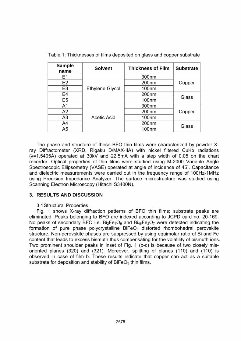
Table 1: Thicknesses of films deposited on glass and copper substrate
Sample name Solvent Thickness of Film Substrate
E1
Ethylene Glycol
300nm Copper E2 200nm
E3 100nm E4 200nm Glass E5 100nm A1
Acetic Acid
300nm Copper A2 200nm
A3 100nm A4 200nm Glass A5 100nm
The phase and structure of these BFO thin films were characterized by powder X-ray Diffractometer (XRD, Rigaku D/MAX-IIA) with nickel filtered CuKα radiations (λ=1.5405Å) operated at 30kV and 22.5mA with a step width of 0.05 on the chart recorder. Optical properties of thin films were studied using M-2000 Variable Angle Spectroscopic Ellipsometry (VASE) operated at angle of incidence of 45˚. Capacitance and dielectric measurements were carried out in the frequency range of 100Hz-1MHz using Precision Impedance Analyzer. The surface microstructure was studied using Scanning Electron Microscopy (Hitachi S3400N).
3. RESULTS AND DISCUSSION
3.1 Structural Properties Fig. 1 shows X-ray diffraction patterns of BFO thin films; substrate peaks are
eliminated. Peaks belonging to BFO are indexed according to JCPD card no. 20-169. No peaks of secondary BFO i.e. Bi2Fe4O9 and Bi46Fe2O7 were detected indicating the formation of pure phase polycrystalline BiFeO3 distorted rhombohedral perovskite structure. Non-perovskite phases are suppressed by using equimolar ratio of Bi and Fe content that leads to excess bismuth thus compensating for the volatility of bismuth ions. Two prominent shoulder peaks in inset of Fig. 1 (b-c) is because of two closely mis-oriented planes (320) and (321). Moreover, splitting of planes (110) and (110) is observed in case of film b. These results indicate that copper can act as a suitable substrate for deposition and stability of BiFeO3 thin films.

Fig. 1: XRD of BFO films prepared under E1, E2 and E3 conditions at room temperature
The most important thing is the polycrystalline nature of BiFeO3 observed in our films without any heat treatment. To the best of our knowledge there is no report on polycrystalline nature of BiFeO3 thin films using chemical methods without heat treatment. Huang et al (2011) reported pure BiFeO3 films on Pt/Ti/Si/SiO2 substrate in the temperature range of 400-500oC using chemical solution deposition method. Sharma et al (2011) prepared nanostructured BiFeO3 thin films on glass substrate via sol-gel and obtained crystalline BiFeO3 phase upon annealing at 450oC. Huang et al (2011) obtained crystalline phase on Si and LaNiO3/Si after crystallizing the films at 600oC. Xiuzhang et al (2010) reported crystalline phase on LaNiO3 coated Si substrate using sol-gel method upon annealing the films at 500oC. Das et al (2010) used wet chemical route and obtained the required phase after annealing the films at 400oC and 500oC. Zhang et al (2010) obtained polycrystalline BiFeO3 thin films, prepared via chemical solution deposition method, upon annealing at 500oC. This literature overview and our XRD results indicate that there is so far no report on polycrystalline pure BiFeO3 films at room temperature, and that copper can act as a suitable substrate for obtaining single phase BFO thin films which is being observed in our case for the first time. We have heat-treated these samples as well, however the detailed results will be presented elsewhere.

Fig. 2 shows a representative scanning electron micrograph of the presently prepared BiFeO3 films. This figure shows a dense surface microstructure with grains of the order of 100nm; the details will be published elsewhere.
Fig. 2: SEM of BFO film
3.2 Dielectric Properties The value of dielectric constant is calculated from the equation:
(1)
Where, ε o is permittivity of free space, d is thickness of the film and A is area of the device.
Dielectric loss, which gives the loss of energy from applied field into the specimen, is given as:
(2)
Where, ρ is the resistivity of the film and f is frequency of the applied field. Frequency dependence of dielectric constant is displayed in Fig. 3. The films show
dispersion in dielectric constant in the range of 100Hz to 10KHz. The dispersion of the dielectric constant with increase in frequency is because of the fact that when electric field is applied, the space-charge carriers require finite time to align their axes in the direction of field. When frequency of the field is increased, the space-charge carriers do

not follow the alteration of the field effectively and a decrease in dielectric constant is observed. At high frequency the reversal of applied field is so high that the charge carriers barely move before the field reverses and thus make no contribution to polarization and hence the steady dielectric constant (Verma 2011).
0 20000 40000 60000 80000 100000
0.00000
0.00001
0.00002
0.00003
A1_as deposited A2 A3 Boltzmann fitting of A1 Boltzmann fitting of A2 Boltzmann fitting of A3
ε'
Frequency(Hz)
0 20000 40000 60000 80000 1000000.00000
0.00001
0.00002
ε'
Frequency(Hz)
A1_ann A2 A3 Boltzmann fitting of A1 Boltzmann fitting of A2 Boltzmann fitting of A3

0 50000 100000 150000 200000 250000 300000 350000 400000
0.0000
0.0001
0.0002
0.0003
0.0004
E1_as E2 E3 Boltzmann fitting for E1 Boltzmann fitting for E2 Boltzmann fitting for E3
ε'
Frequency(Hz)
0 20000 40000 60000 80000 100000
0.00000
0.00001
0.00002
0.00003
0.00004
0.00005
E1_ann E2 E3 Boltzmann fitting of E1 Boltzmann fitting of E2 Boltzmann fitting of E3
ε'
Frequency(Hz)
Fig. 3: Dielectric constant for films under as-deposited and annealing conditions
It is observed that dielectric constant of films increases with increase in film thickness. However, there is a decrease of dielectric constant upon annealing. The values of dielectric constant are quite low as compared to the reported values (Tang 2012, Kim 2012, Ahmed 2012). It is well known that dielectric properties of thin films are affected by both intrinsic and extrinsic properties. Among the intrinsic parameters film orientation, grain boundaries and dielectric response of single domain is extremely important. Decrease in grain size can lead to increase in internal stresses to inhibit the formation of 180˚ domain thus causing a decrease in dielectric constant of some multiferroic thin films (Tang 2012). Extrinsic effects arise from strain/stress from substrate clamping and pinning of domain boundary due to domain wall motion (Tang 2012). The dielectric dispersion curve is explained on the basis of Koop’s theory based

on Maxwell-Wanger model according to which grain boundaries are found to be more effective in low frequency region while grains are more effective in high frequency region. In the nanoregime, both grains and grain boundaries are found to be in large numbers as compared to that in bulk. So the relatively small dielectric constant is because of the large grain boundaries due to large dc resistivity. In low frequency regime, dc resistivity exhibits a more dominant role in determining the dielectric properties as compared with the electronic and ionic polarization (Verma 2011).
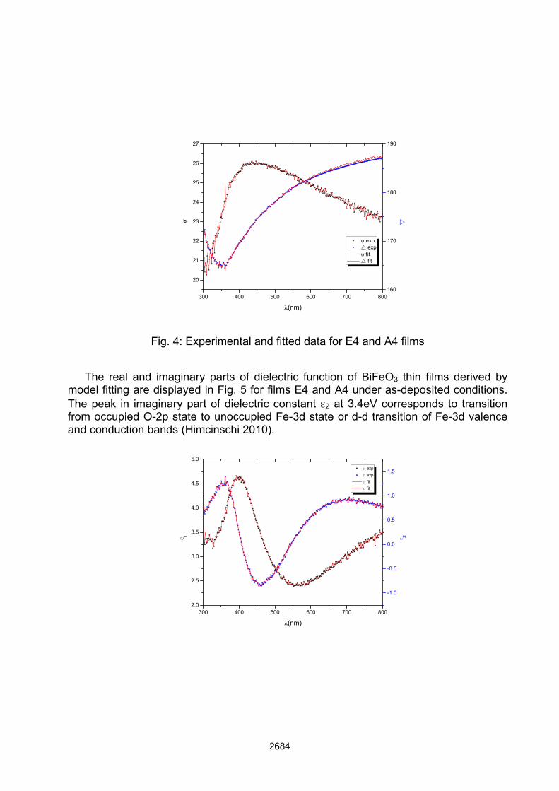
3.3 Optical Properties ∆ and ψ can be represented as mathematical functions relating to the material
characteristics. Hence, a mathematical model dependent analysis has to be performed to determine the required parameters from measured ellipsometric data. Measured and fitted data of ψ and ∆ for films E4 and A4 are shown in Fig. 4. Cauchy model is used to fit the experimental data in the transparent spectral region. A good fit between the model and experimental data over the entire wavelength range can be seen in this figure.
300 400 500 600 700 800
18
20
22
24
26
ψ exp exp ψ fit fit
λ(nm)
ψ
170
180
190
300 400 500 600 700 800
20
21
22
23
24
25
26
27
ψ
λ(nm)
160
170
180
190
ψ exp exp ψ fit fit
Fig. 4: Experimental and fitted data for E4 and A4 films
The real and imaginary parts of dielectric function of BiFeO3 thin films derived by model fitting are displayed in Fig. 5 for films E4 and A4 under as-deposited conditions. The peak in imaginary part of dielectric constant ε2 at 3.4eV corresponds to transition from occupied O-2p state to unoccupied Fe-3d state or d-d transition of Fe-3d valence and conduction bands (Himcinschi 2010).
300 400 500 600 700 8002.0
2.5
3.0
3.5
4.0
4.5
5.0 ε
1 exp
ε2 exp
ε1 fit
ε2 fit
λ(nm)
ε 1
-1.0
-0.5
0.0
0.5
1.0
1.5
ε2

300 400 500 600 700 800
2.5
3.0
3.5
4.0
4.5
5.0 ε
1 exp
ε2 exp
ε1 fit
ε2 fit
λ(nm)
ε 1
-1.0
-0.5
0.0
0.5
1.0
1.5
2.0ε2
Fig. 5: Real and imaginary parts of dielectric constant for films E4 and A4
Dielectric constants, ε 1 and ε 2, and optical constants, n and k are given by:
(3)
(4)
Refractive index of BFO thin films is shown in Fig. 6. Obviously, n changes with wavelength analogous to normal dispersion. A peak of refractive index at varying wavelengths by changing the thickness and under annealing conditions corresponds to direct band gap transition. Moreover a general trend is seen that with increasing the thickness refractive index decreases, whereas upon annealing the refractive index increases. This increase may be attributed to higher packing density and a change in crystalline structure. Values of refractive index under as-deposited conditions are lower than earlier reported values but upon annealing our values are in good agreement with refractive index reported for thin films. (Huang 2010, Li 2007, Bi 2008).

300 400 500 600 700 8001.6
1.8
2.0
2.2
2.4
2.6
2.8
n
λ(nm)
A4_as-deposited A5_as-deposited A4_annealed A5_annealed
300 400 500 600 700 800
1.75
1.80
1.85
1.90
1.95
2.00
2.05
2.10
2.15
2.20
2.25
2.30
2.35
n
λ(nm)
E4_as deposited E4_annealed E5_As deposited E5_annealed
Fig. 6: Refractive index vs. wavelength for BFO thin films
Absorption coefficient is one of the most important factors in studying the optical properties of ferroelectrics. The absorption coefficient ‘α’ of BFO thin films is deduced from extinction coefficient using
(5)
The direct band gap is extracted by linear extrapolation of α2(m-2) vs. E(eV) plot to zero on the energy axis. A typical such plot is shown in Fig. 7.

0.00E+002.00E+124.00E+126.00E+128.00E+121.00E+131.20E+131.40E+131.60E+131.80E+132.00E+13
1.5 1.7 1.9 2.1 2.3 2.5 2.7 2.9 3.1 3.3 3.5
Alp
ha
^2
(/m
^2
)
Energy (eV)
Fig. 7: A representative plot of absorption coefficient vs. energy for BiFeO3 thin film
Band gap is known as a finger print of material at bulk level but at nanoscale, it is always observed that band gap varies with film thickness. This is because of changes in barrier height at grain boundaries with thickness due to high density of dislocations or because of quantum size effect. The optical band gap values of BiFeO3 thin films come out to be in the range 2.715-2.72 eV. Park et al (2011) reported a band gap of 2.7eV, Himcinschi et al (2010) reported a band gap of 2.75eV, Zelezny et al (2010) reported a band gap of 2.70-2.70eV, Bi et al (2008) reported a band gap of 2.44eV, and Cheng et al (2012) reported a band gap of 2.72eV. The band gap values in our case in line with most of the referenced above.
3.4 Electrical and Magnetic Hysteresis As mentioned earlier, interest in these BiFeO3 thin films was their existence as both
ferroelectric and ferromagnetic material at the same time. The detailed results of electric and magnetic properties will be presented elsewhere. However, in order to prove that both magnetic and electrical hysteresis existed in these, sol-gel deposited thin films the initial results are presented in Figs. 8&9.
Fig. 8: Electrical hysteresis curve of BiFeO3 film

Fig. 9: Magnetic hysteresis of BiFeO3 film
CONCLUSION
In summary, when the solvent is changed in the sol-gel process, chemical reactions are changed the phases and lattice parameters of thin films are affected by these variations. This leads to changes in structural, dielectric and magnetic properties. Two different solvents, ethylene glycol and acetic acid, in sol-gel route were employed in this work. Polycrystalline single phase BiFeO3 films have been obtained under as-deposited and annealing conditions for both the solvents. The dielectric values of BFO thin films are quite low as compared to bulk BFO due to the enhanced effect of grain boundaries. Refractive index of the films is in the range of 1.93-2.65 and increased upon annealing. Band gap of the films is of the order of 2.7eV.
REFERENCES
Ahmed, T., Vorobiev, A. and Gevorgian, S. (2012), “Growth temperature dependent dielectric properties of BiFeO3 thin films deposited on silica glass substrates.” Thin Solid Films, Vol. 520, 4470–4474. Bi, L., Taussig, A.R., Kim, H.S., Wang, L., Dionne, G.F., Bono, D., Pearsson, K., Ceder, G. and Ross, C.A. (2008), “Structural, magnetic, and optical properties of BiFeO3 and Bi2FeMnO6 epitaxial thin films: An experimental and first-principles study” Phys. Rev. B, Vol. 78, 104106-1-10. Cheng, L.B., Le, C.C. and Xin, J.K. (2012), “Photo-induced properties of BiFeO3 films.” Mater. Chem. Phys., Vol. 132, 364–367. Das, S., Basu, S., Mitra, S., Chakravorty, D. and Mondal, B.N. (2010), “Wet chemical route to transparent BiFeO3 films on SiO2 substrates.” Thin Solid Films, Vol. 518, 4071–4075. Himcinschi, C., Vrejoiu, I., Friedrich, M., Nikulina, E., Ding, L., Cobet, C., Esser, N., Alexe, M., Rafaja, D. and Zahn, D.R.T. (2010), “Substrate influence on the optical and structural properties of pulsed laser deposited BiFeO3 epitaxial films.” J. Appl. Phys., Vol. 107, 123524-1-5.

Huang, A. and Shannigrahi, S.R. (2011), “Structural and electrical properties of BiFeO3 thin films by solution deposition and microwave annealing.” Thin Solid Films, Vol. 519, 4793–4797. Huang, D., Deng, H., Yang, P. and Chu, J. (2010), “Optical and electrical properties of multiferroic bismuth ferrite thin films fabricated by sol–gel technique.” Mater. Lett., Vol. 64, 2233–2235. Kim, A.Y., Han, S.H., Kang, H.W., Lee, H.G., Kim, J.S. and Cheon, C.I. (2012), “Dielectric and magnetic properties of BiFeO3 ceramics prepared by hydrothermal synthesis.” Ceram. Int., Vol. 38, S397–S401. Li, Y.W., Xue, J.Q., Sun, J.L., Meng, X.J., Huang, Z.M., Chu, J.H., Ding, L.H. and Zhang, W.F. (2007), “Infrared optical properties of BiFeO3 thin films prepared by chemical solution deposition.” Appl. Phys. A, Vol. 87, 125–128. Park, J.M, Gotoda, F., Kanashima, T. and Okuyama, M. (2011), “Preparation and characterization of BiFeO3 thin films deposited on ITO substrates by using pulsed laser deposition.” J. Korean Phys. Soc., Vol. 59(3) 2537-2541. Quan, Z., Hu, H., Xu, S., Liu, W., Fang, G., Li, M. and Zhao, X. (2008), “Surface chemical bonding states and ferroelectricity of Ce-doped BiFeO3 thin films prepared by sol–gel process.” J. Sol-Gel Sci. Technol., Vol. 48, 261–266. Safi, R. and Shokrollahi, H. (2012), “Physics, chemistry and synthesis methods of nanostructured bismuth ferrite (BiFeO3) as a ferroelectro-magnetic material.” Prog. Solid State Chem., doi:10.1016/j.progsolidstchem.2012.03.001. Sharma, H.B., Singh, S.B. and Singh, N.B. (2011), “Structural and optical properties of low temperature synthesized nanostructured BiFeO3 thin films.” Physica B, Vol. 406, 351–353. Tang, X., Dai, J., Zhu, X., Lin, J., Chang, Q., Wu, D., Song, W. and Sun, Y. (2012), “Thickness-dependent dielectric, ferroelectric, and magnetodielectric properties of BiFeO3 thin films derived by Chemical Solution Deposition.” J. Am. Ceram. Soc., Vol. 95(2), 538–544. Verma, K.C., Ram, M., Singh, J. and Kotnala, R.K. (2011), “Impedance spectroscopy and dielectric properties of Ce and La substituted Pb0.7Sr0.3(Fe0.012Ti0.988)O3 nanoparticles.” J. Alloys Compd., Vol. 509, 4967–4971. W. Xiuzhang, Y. Bowu, D. Zhigao, L. Meifeng, X. Shengxiang, L. Wenqing, L. Hongri, J. (2010), “Effect of annealing temperature on the ferroelectric properties of BiFeO3 thin films prepared by sol-gel process.” J. Wuhan Univ. Technol.– Mater. Sci. Ed., Vol. 25(3), 384-387. Xu, J.H., Ke, H., Jia, D.C., Wang, W. and Zhou, Y. (2009), “Low-temperature synthesis of BiFeO3 nanopowders via a sol–gel method.” J. Alloys Compd., Vol. 472, 473-477. Zelezny, V., Chvostova, D., Pajasova, L., Vrejoiu, I. and Alexe, M. (2010), “Optical properties of epitaxial BiFeO3 thin films” Appl. Phys. A, Vol. 100, 1217–1220. Zhang, H., Chen, X., Wang, T., Wang, F. and Shi, W. (2010), “Structure and electrical properties of BiFeO3 thin films grown on LaNiO3 electrode by chemical solution deposition” J. Alloys Compd., Vol. 500, 46–48. Zhang, S., Wang, L., Gao, Z., Zhang, X., Wang, W. and Ma, Y. (2011), “Ferromagnetism in sub-micron scale BiFeO3.” Mater. Lett., Vol. 65, 3309–3312.