Thin Solid Films - SPM
9
Effect of vacuum magnetic annealing on the structural and physical properties of the Ni and Al co-doped ZnO films Mingpeng Yu a , Hong Qiu a, ⁎, Xiaobai Chen b a Department of Physics, School of Applied Science, University of Science and Technology Beijing, 30 Xueyuan Road, Haidian District, Beijing 100083, China b College of Mechanical Engineering, Beijing Technology and Business University, Beijing 100048, China abstract article info Article history: Received 14 October 2009 Received in revised form 9 July 2010 Accepted 12 July 2010 Available online 16 July 2010 Keywords: Ni and Al co-doped Zinc oxide Thin films Magnetic annealing Structural properties Ferromagnetism Carrier transport Magnetization behavior Sputtering About 300 nm-thick Zn 0.87 Al 0.06 Ni 0.07 O, Zn 0.83 Al 0.06 Ni 0.11 O and Zn 0.81 Al 0.04 Ni 0.15 O films were deposited on glass substrates at 300 K by co-sputtering ZnO:Al and Ni targets. The films were annealed in vacuum at 673 K for 2 h under a magnetic field of 4.8×10 4 A/m applied along the film plane and then were cooled down to room temperature without magnetic field. All the films have a wurtzite structure and consist of thin columnar grains perpendicular to the substrate. The annealing promotes the (002) orientation growth in the film growing direction for the Zn 0.87 Al 0.06 Ni 0.07 O and Zn 0.83 Al 0.06 Ni 0.11 O films as well as the (100) orientation growth for the Zn 0.81 Al 0.04 Ni 0.15 O film. The annealing results in a slight increase in the grain size. A weak Ni diffraction peak was detected for the annealed films with high Ni content. The annealing enhances the room temperature ferromagnetism of the films. A temperature dependence of magnetization confirms that the Curie temperature is above 400 K for the annealed films. The films magnetically annealed exhibit an anisotropic magnetization behavior. The annealed Zn 0.87 Al 0.06 Ni 0.07 O film has the lowest resisti- vity (8.73 × 10 −3 Ω cm), the highest free electron concentration (1.73 × 10 20 cm −3 ) and Hall mobility (4.16 cm 2 V −1 s −1 ). A temperature dependence of the resistivity from 50 K to 300 K reveals that the carrier transport mechanism is Mott's variable range hopping in the low temperature range and thermally activated band conduction in the high temperature range. © 2010 Elsevier B.V. All rights reserved. 1. Introduction ZnO films co-doped with Al and transition metals are important function materials for optoelectronic and magnetoelectronic applica- tions. The transition metals generally used are Co and Mn [1–5]. Recently, we have prepared the Ni and Al co-doped ZnO films on glass substrates by direct current (DC) magnetron co-sputtering [6,7]. The films had the room temperature ferromagnetism, dependent on the deposition temperature and the Ni content. Furthermore, the film, which exhibited the better ferromagnetic behavior, had the relatively high resistivity. It is a significant work to prepare the Ni and Al co- doped ZnO films having better electrical and ferromagnetic behaviors for their potential applications. Annealing could improve the structural and physical properties of ZnO films doped with transition metals. Cho et al. [8] heat-treated CoFe doped ZnO films at 823 K for 10 min by rapid thermal annealing under vacuum. They found that the rapid thermal annealing led to a remarked increase in the magnetization and the electron concentra- tion of the films. Hsu et al. [9] investigated systematically the annealing effect on structure and magnetism for Co doped ZnO films under air, Ar and Ar/H 2 atmospheres at 523 K. The saturation magnetization varied drastically for the different annealing processes. They found that the ferromagnetism of the films was strongly correlated with the oxygen vacancies in the ZnO lattice. Khare et al. [10] annealed Zn 0.98 Co 0.02 O films in reducing or oxidizing atmosphere at 673 K. They observed that the magnetization of the film decreased after every annealing regardless of reducing or oxidizing atmosphere. Huang et al. [11] reported that for the Co doped ZnO films annealed in air the saturation magnetization decreased with increasing annealing temperature. Liu et al. [12] sputter-deposited Ni doped ZnO films and heat-treated them by rapid thermal annealing at 1073 K for 10 min in Ar gas environment. They found that the heat-treatment increased markedly the magnetization of the films and destroyed the ZnO crystallinity. Among many techniques to prepare materials, magnetic field annealing plays an important role on microstructures and magnetic properties of the magnetic materials. Harada et al. [13] reported an effect of magnetic field annealing on grain growth in nanocrystalline Ni produced by electrodeposition. Chung et al. [14] found that Ni tapes magnetically annealed showed a stronger texture and a better magnetic domain structure than those annealed without magnetic field. Coisson et al. [15] prepared 30 nm-thick Co 50 Fe 50 films on glass substrates by sputtering and annealed the films under a magnetic field of 100 Oe. They found that the magnetic field annealing affected the Thin Solid Films 518 (2010) 7174–7182 ⁎ Corresponding author. Tel.: +86 10 62333786. E-mail address: [email protected] (H. Qiu). 0040-6090/$ – see front matter © 2010 Elsevier B.V. All rights reserved. doi:10.1016/j.tsf.2010.07.045 Contents lists available at ScienceDirect Thin Solid Films journal homepage: www.elsevier.com/locate/tsf
Transcript of Thin Solid Films - SPM

Thin Solid Films 518 (2010) 7174–7182
Contents lists available at ScienceDirect
Thin Solid Films
j ourna l homepage: www.e lsev ie r.com/ locate / ts f
Effect of vacuum magnetic annealing on the structural and physical properties of theNi and Al co-doped ZnO films
Mingpeng Yu a, Hong Qiu a,⁎, Xiaobai Chen b
a Department of Physics, School of Applied Science, University of Science and Technology Beijing, 30 Xueyuan Road, Haidian District, Beijing 100083, Chinab College of Mechanical Engineering, Beijing Technology and Business University, Beijing 100048, China
⁎ Corresponding author. Tel.: +86 10 62333786.E-mail address: [email protected] (H. Qiu).
0040-6090/$ – see front matter © 2010 Elsevier B.V. Adoi:10.1016/j.tsf.2010.07.045
a b s t r a c t
a r t i c l e i n f oArticle history:Received 14 October 2009Received in revised form 9 July 2010Accepted 12 July 2010Available online 16 July 2010
Keywords:Ni and Al co-doped Zinc oxideThin filmsMagnetic annealingStructural propertiesFerromagnetismCarrier transportMagnetization behaviorSputtering
About 300 nm-thick Zn0.87Al0.06Ni0.07O, Zn0.83Al0.06Ni0.11O and Zn0.81Al0.04Ni0.15O films were deposited onglass substrates at 300 K by co-sputtering ZnO:Al and Ni targets. The films were annealed in vacuum at 673 Kfor 2 h under a magnetic field of 4.8×10⁴ A/m applied along the film plane and then were cooled down toroom temperature without magnetic field. All the films have a wurtzite structure and consist of thincolumnar grains perpendicular to the substrate. The annealing promotes the (002) orientation growth in thefilm growing direction for the Zn0.87Al0.06Ni0.07O and Zn0.83Al0.06Ni0.11O films as well as the (100) orientationgrowth for the Zn0.81Al0.04Ni0.15O film. The annealing results in a slight increase in the grain size. A weak Nidiffraction peak was detected for the annealed films with high Ni content. The annealing enhances theroom temperature ferromagnetism of the films. A temperature dependence of magnetization confirmsthat the Curie temperature is above 400 K for the annealed films. The films magnetically annealed exhibitan anisotropic magnetization behavior. The annealed Zn0.87Al0.06Ni0.07O film has the lowest resisti-vity (8.73×10⁻³Ω cm), the highest free electron concentration (1.73×1020 cm−3) and Hall mobility (4.16cm2V−1 s−1). A temperature dependence of the resistivity from 50 K to 300 K reveals that the carriertransport mechanism is Mott's variable range hopping in the low temperature range and thermally activatedband conduction in the high temperature range.
ll rights reserved.
© 2010 Elsevier B.V. All rights reserved.
1. Introduction
ZnO films co-doped with Al and transition metals are importantfunction materials for optoelectronic and magnetoelectronic applica-tions. The transition metals generally used are Co and Mn [1–5].Recently, we have prepared the Ni and Al co-doped ZnO films on glasssubstrates by direct current (DC) magnetron co-sputtering [6,7]. Thefilms had the room temperature ferromagnetism, dependent on thedeposition temperature and the Ni content. Furthermore, the film,which exhibited the better ferromagnetic behavior, had the relativelyhigh resistivity. It is a significant work to prepare the Ni and Al co-doped ZnO films having better electrical and ferromagnetic behaviorsfor their potential applications.
Annealing could improve the structural and physical properties ofZnO films doped with transition metals. Cho et al. [8] heat-treatedCoFe doped ZnO films at 823 K for 10 min by rapid thermal annealingunder vacuum. They found that the rapid thermal annealing led to aremarked increase in the magnetization and the electron concentra-tion of the films. Hsu et al. [9] investigated systematically theannealing effect on structure and magnetism for Co doped ZnO
films under air, Ar and Ar/H2 atmospheres at 523 K. The saturationmagnetization varied drastically for the different annealing processes.They found that the ferromagnetism of the films was stronglycorrelated with the oxygen vacancies in the ZnO lattice. Khare et al.[10] annealed Zn0.98Co0.02O films in reducing or oxidizing atmosphereat 673 K. They observed that the magnetization of the film decreasedafter every annealing regardless of reducing or oxidizing atmosphere.Huang et al. [11] reported that for the Co doped ZnO films annealed inair the saturation magnetization decreased with increasing annealingtemperature. Liu et al. [12] sputter-deposited Ni doped ZnO films andheat-treated them by rapid thermal annealing at 1073 K for 10 min inAr gas environment. They found that the heat-treatment increasedmarkedly the magnetization of the films and destroyed the ZnOcrystallinity.
Among many techniques to prepare materials, magnetic fieldannealing plays an important role on microstructures and magneticproperties of the magnetic materials. Harada et al. [13] reported aneffect of magnetic field annealing on grain growth in nanocrystallineNi produced by electrodeposition. Chung et al. [14] found that Ni tapesmagnetically annealed showed a stronger texture and a bettermagnetic domain structure than those annealed without magneticfield. Coisson et al. [15] prepared 30 nm-thick Co50Fe50 films on glasssubstrates by sputtering and annealed the films under amagnetic field of100 Oe. They found that the magnetic field annealing affected the

Fig. 1. XRD patterns of the Ni and Al co-doped ZnO films; (a) Zn0.87Al0.06Ni0.07O film, as-deposited, (b) Zn0.83Al0.06Ni0.11O film, as-deposited, (c) Zn0.81Al0.04Ni0.15O film, as-deposited, (d) Zn0.87Al0.06Ni0.07O film, annealed, (e) Zn0.83Al0.06Ni0.11O film, annealed,(f) Zn0.81Al0.04Ni0.15O film, annealed. The standard diffraction pattern of wurtzitehexagonal ZnO is also shown.
7175M. Yu et al. / Thin Solid Films 518 (2010) 7174–7182
ferromagnetic behaviors of the films. It has not been reported howa vacuum magnetic annealing influences structural and physicalproperties of the ZnO-based films doped with transition metals. Inthe present work, Zn0.87Al0.06Ni0.07O, Zn0.83Al0.06Ni0.11O andZn0.81Al0.04Ni0.15O films are deposited on glass substrates at300 K by co-sputtering ZnO:Al and Ni targets. Then the films areannealed in vacuum under a magnetic field applied along the filmplane. The structure of the films is studied using X-ray diffraction(XRD), atomic force microscopy (AFM) and field emission scanningelectron microscopy (FE-SEM). The magnetic, electrical andsemiconducting properties are measured by using a vibratingsample magnetometer (VSM) and the van der Pauw method. Acarrier transport mechanism is discussed by measuring thetemperature-dependent resistivity of the films.
2. Experimental procedure
The DC magnetron sputtering system used (KYKY TechnologyDevelopment Ltd.), which has two targets inclined at an angle of 45°to the same substrate, has been described elsewhere in detail [16].One target was a sintered ceramic ZnO+2 wt.%Al2O3 target (99.99%in purity) with 50 mm in diameter and the other was a Ni target(99.99% in purity) with 50 mm in diameter. The distance between thetarget and the substrate was about 100 mm. A load-lock chamber wasused to prevent the working chamber from air during changing asample. The glass substrates were ultrasonically rinsed in acetone, indeionized water and in ethanol. About 300 nm-thick Ni and Al co-doped ZnO films were deposited on glass substrates at 300 K by co-sputtering under an Ar gas (99.9995% in purity) pressure of 1 Pa.During the sputter-deposition, the sputtering power applied to theZnO+2 wt.%Al2O3 target was fixed at 200 W and that applied to theNi target was respectively adjusted to 10 W, 14 W and 18 W inorder to control the Ni content in the films. According to the energydispersive X-ray spectroscopy analysis, the Zn0.87Al0.06Ni0.07O,Zn0.83Al0.06Ni0.11O and Zn0.81Al0.04Ni0.15O films were obtained.The deposition rate was about 0.25 nm/s and the deposition timewas 20 min. The substrate holder was rotated using a steppingmotor during deposition in order to obtain a uniformly thick film.Prior to deposition, the working chamber was evacuated to apressure lower than 2×10⁻⁴ Pa using a turbo molecular pump.
Magnetic annealing was carried out in vacuum lower than2×10−3 Pa. After the heat-treatment chamber was evacuated using aturbo molecular pump, the Ni and Al co-doped ZnO films were heated to673 K without magnetic field and then were annealed at 673 K for 2 hunder a magnetic field of 4.8×10⁴ A/m applied along the film plane.Finally, the films were cooled down to room temperature withoutmagnetic field.
XRD (Rigaku Co.) was used to analyze the crystalline orientation andthe lattice constant of the films. The XRD measurements wereperformed in a standard θ–2θ scan using a Cu Kα radiation filtered bya crystal monochromator (wavelength λ=0.15417 nm). The X-raysource was operated at a power of 40 kV×200 mA. Scan speed was0.1 deg/s and scan step was 0.02° . FE-SEM (Zeiss Co.) was used toobserve the crystalline structure of the films. Surface smoothness andmorphology of the films were investigated using AFM of CSPM5000(Ben Yuan Ltd.).
A magnetization curve of the films was measured at roomtemperature using VSM (Quantum Design Co.). The magnetic fieldwas applied along the film plane during the VSM measurement. Themagnetization data of the film were calibrated by subtracting thesignal of the substrate. A temperature dependence of the magnetiza-tion for the annealed Ni and Al co-doped films was measured from50 K to 400 K. First, the film was cooled down to 50 K at zero field.Then the magnetization data were taken with warming up under amagnetic field of 8.0×10⁴ A/m applied along the film plane. Thewarming rate is approximate to 5 K/min. The resistivity and the Hall
coefficient of the films were measured at room temperature using thevan der Pauwmethod. The carrier concentration and the Hall mobilitywere calculated in terms of the resistivity and the Hall coefficient. Atemperature dependence of the resistivity for the films was measuredin the temperature range of 50–300 K (Quantum Design Co.).
3. Results and discussion
3.1. Structure
Fig. 1 shows XRD patterns of the Ni and Al co-doped ZnO films as-deposited and magnetically annealed. As can be seen from Fig. 1, all thefilmshave awurtzite structure. For the as-depositedfilms, theZnO(100),ZnO(002), ZnO(101) and ZnO(110) diffraction peaks are observed. Forthe annealed films, the Zn0.87Al0.06Ni0.07O and Zn0.83Al0.06Ni0.11O filmsmainly show the ZnO(002) peak and the Zn0.81Al0.04Ni0.15O film mainlyexhibits the ZnO(100) peak. It indicates that the annealing promotes c-axis preferential orientation growth for the Zn0.87Al0.06Ni0.07O andZn0.83Al0.06Ni0.11O films as well as the (100) preferential orientationgrowth for the Zn0.81Al0.04Ni0.15O film. Using the measured XRD peakintensity, the texture coefficientY(hkl) of aplane (hkl) for thefilmcanbegiven by
YðhklÞ = IðhklÞ= IbðhklÞ∑ð1 =NÞ × ½IðhklÞ= IbðhklÞ�
ð1Þ
where I(hkl) is the measured XRD peak intensity of the plane (hkl) ofthe film, Ib(hkl) the standard XRD peak intensity of the plane (hkl)and N the number of the reflection diffraction peak [17]. In this case,the value of Ib(hkl) comes from that of the ZnO bulk [18]. The Y valuesof the as-deposited films are summarized in Table 1. As shown inTable 1, for the as-deposited films the c-axis preferential orientationin the film growing direction weakens with increasing the Ni content.It is consistent with the result reported previously [7]. It is consideredthat large amounts of Ni atoms as impurity influence a nucleation at
zhk
线条
zhk
线条

Table 1Texture coefficients Y of the as-deposited films.
Film Y(100) Y(002) Y(101) Y(110)
Zn0.87Al0.06Ni0.07O 0.75 1.97 0.81 0.47Zn0.83Al0.06Ni0.11O 1.66 0.60 0.72 1.02Zn0.81Al0.04Ni0.15O 1.57 0.58 0.60 1.25
7176 M. Yu et al. / Thin Solid Films 518 (2010) 7174–7182
the initial stage of the film growth and incorporate in the growingfilms, resulting in a deterioration of the c-axis preferential orientationof the films. No diffraction peaks of Ni, Al and their oxides are detectedfor the as-deposited films. However, the Ni(111) diffraction peak isobserved for the Zn0.83Al0.06Ni0.11O and Zn0.81Al0.04Ni0.15O filmsmagnetically annealed. The mean crystallite size D of Ni can begiven by Scherrer's equation
D =0:89λβcosθ
ð2Þ
where λ is the X-ray wavelength (0.15417 nm) and β the half-heightwidth of the X-ray diffraction peak. θ is the Bragg angle. Using Eq. (2),according to the β value of the Ni(111) peak, the mean crystallite sizeof Ni is calculated to be about 20 nm. It is considered that the Ni nano-clusters exist in the Ni and Al co-doped ZnO films as-deposited andannealed although they can't be detected by XRD for the as-depositedfilms. We do not exclude the possibility forming the Ni nano-clusterssmall enough not to be detected by XRD. The Ni nano-clusters couldexist at the grain boundaries in the polycrystalline films consisting offine grains. After the films were magnetically annealed, the Ni nano-clusters grew and could be detected by XRD. In fact, X-rayphotoelectron spectroscopy has also revealed that the metallic Niexisted in the Ni and Al co-doped ZnO films [19].
According to the XRD measurements, spacings of the (100),(002), (101) and (110) planes in the Ni and Al co-doped ZnO filmscan be obtained. Then the lattice volume of the films as-depositedand annealed are calculated and summarized in Table 2. As shown inTable 2, for the as-deposited Zn0.87Al0.06Ni0.07O film, the latticevolume is smaller than that of the ZnO bulk (47.62×10⁻³ nm) [18].Ionic radii of Al3+ (0.57 Å) and Ni2+ (0.69 Å) are smaller than ionicradius of Zn2+ (0.74 Å). Therefore, the substitution of the Al3+ and/or Ni2+ ions for the Zn2+ ions results in the decrease in thelattice volume of the as-deposited Zn0.87Al0.06Ni0.07O film. For theZn0.83Al0.06Ni0.11O and Zn0.81Al0.04Ni0.15O films, their lattice volumesare larger than that of the ZnO bulk. Furthermore, the lattice volumeincreases with increasing the Ni content. It suggests that some Niand/or Al atoms enter into the interstitial sites of the ZnO lattice. Thelattice volumes of the annealed films shrink compared with the as-deposited films and are smaller than that of the ZnO bulk. It meansthat the interstitial Ni atoms aggregate forming the Ni clustersduring the magnetic annealing process. The Ni clusters could exist atthe grain boundaries for the polycrystalline films. It should be notedthat the Ni(111) diffraction peak from the Ni nano-clusters has beenobserved for the Zn0.83Al0.06Ni0.11O and Zn0.81Al0.04Ni0.15O filmsmagnetically annealed.
Fig. 2 shows FE-SEM microphotographs of the Ni and Al co-dopedZnO films as-deposited and magnetically annealed. As can be seen
Table 2Lattice volumes of the as-deposited and annealed films.
Film Treatment Lattice volume (×10−3 nm3)
Zn0.87Al0.06Ni0.07O As-deposited 47.53Zn0.83Al0.06Ni0.11O As-deposited 47.82Zn0.81Al0.04Ni0.15O As-deposited 48.12Zn0.87Al0.06Ni0.07O Annealed 47.41Zn0.83Al0.06Ni0.11O Annealed 46.96Zn0.81Al0.04Ni0.15O Annealed 47.22
from Fig. 2, all the films growwith thin columnar grains perpendicularto the substrate. Fig. 3 show AFM images of the Ni and Al co-dopedZnO films as-deposited andmagnetically annealed. As shown in Fig. 3,the grain size of the films slightly decreases with increasing the Nicontent. It is attributed to the impurity effect of Ni on the filmstructure. Namely, the more Ni atoms as impurity can lead to a highnucleation density at the initial stage of the film growth, decreasingthe grain size of the film. The magnetic annealing promotes a slightgrowth of the grain size. Root mean square (RMS) roughnesses of theZn0.87Al0.06Ni0.07O, Zn0.83Al0.06Ni0.11O and Zn0.81Al0.04Ni0.15O films as-deposited are 4.6±0.1 nm, 4.3±0.1 nm and 5.0±0.1 nm, respec-tively. After magnetically annealed, the RMS roughness of theZn0.83Al0.06Ni0.11O film doesn't change markedly whereas the rough-ness of the Zn0.87Al0.06Ni0.07O film decreases to 2.48±0.07 nm andthat of the Zn0.81Al0.04Ni0.15O film increases to 6.0±0.2 nm.
3.2. Magnetic properties
Fig. 4 shows magnetization curves of the Ni and Al co-doped ZnOfilms as-deposited and magnetically annealed. For the films as-deposited, the Zn0.87Al0.06Ni0.07O film doesn't show any magneticbehavior whereas the Zn0.83Al0.06Ni0.11O and Zn0.81Al0.04Ni0.15Ofilms exhibit magnetic hysteresis loops at room temperature,meaning that they have the room temperature ferromagnetism.After magnetically annealed, the Zn0.87Al0.06Ni0.07O film also has theroom temperature ferromagnetism as shown in Fig. 4. Furthermore,the magnetic annealing markedly increases the saturation magne-tization and the coercive force of the films. As a comparison, the Niand Al co-doped films were annealed in vacuum at 673 K withoutmagnetic field and their magnetization curves were measured byVSM. Fig. 5 shows the magnetization curves of the Ni and Al co-doped ZnO films annealed without magnetic field. Comparing Fig. 4with Fig. 5, it can be concluded that the magnetic annealing moreeffectively enhances the saturation magnetization of the Ni and Alco-doped ZnO films relative to the annealing without magnetic field.In the present work, according to the XRD results, it is believed thatthe room temperature ferromagnetism of the films is attributed tothe Ni nano-clusters forming in the films. It has been reported thatfor the Co doped ZnO films the room temperature ferromagnetismoriginates from the nano-sized Co clusters [20]. It has also beensuggested that the ferromagnetism in the Co doped ZnO bulk isprobably due to small clusters of second phase segregation [21]. Forthe as-deposited Zn0.87Al0.06Ni0.07O film, the Ni nano-clusters are toosmall to exhibit the room temperature ferromagnetism due to a lowCurie temperature. The Curie temperature of the Ni nanocrystalsdecreased with decreasing the nanocrystal size and decreaseddramatically when the nanocrystal size decreased below 10 nm[22]. For the Ni and Al co-doped ZnO films, the high Ni content andthemagnetic annealing increase the size of the Ni nano-clusters. As aresult, the Zn0.83Al0.06Ni0.11O and Zn0.81Al0.04Ni0.15O films as well asall the films annealed exhibit the room temperature ferromagne-tism. The high saturationmagnetization, residual magnetization andcoercivity of the Zn0.81Al0.04Ni0.15O film magnetically annealed areattributed to a good crystallinity of the Ni nano-clusters.
Fig. 6 shows a temperature dependence of themagnetization (M–Tcurve) for the Ni and Al co-doped ZnO filmsmagnetically annealed. Ascan be seen from Fig. 6, the Curie temperature is above 400 K for theannealed films. Furthermore, the annealed Zn0.81Al0.04Ni0.15O film hasthe least variation of magnetization with temperature. It has beenreported that nanostructured Ni films with a porous thin columnargrains exhibited a faster decrease in the saturation magnetizationwith temperature and a lower Curie temperature compared with thefilms having a good crystallinity [23]. Therefore, it is considered thatthe Ni nano-clusters in the Zn0.81Al0.04Ni0.15O film magneticallyannealed have a good crystallinity, resulting in the least variation ofmagnetization with temperature.

Fig. 2. FE-SEMmicrophotographs of the Ni and Al co-doped ZnO films; (a) Zn0.87Al0.06Ni0.07O film, as-deposited, (b) Zn0.83Al0.06Ni0.11O film, as-deposited, (c) Zn0.81Al0.04Ni0.15O film,as-deposited, (d) Zn0.87Al0.06Ni0.07O film, annealed, (e) Zn0.83Al0.06Ni0.11O film, annealed, (f) Zn0.81Al0.04Ni0.15O film, annealed.
7177M. Yu et al. / Thin Solid Films 518 (2010) 7174–7182
Fig. 7 shows the magnetization curves of the Ni and Al co-dopedfilms magnetically annealed, in which the magnetic field is appliedparallel and perpendicular to the direction of the annealingmagnetic field during the VSM measurements, respectively. Asshown in Fig. 7, all the films exhibit an anisotropic magnetizationbehavior. The saturation magnetization and residual magnetizationof the film at a measurement field parallel to the annealing field arelarger than those of the film at a measurement field perpendicular tothe annealing field. It indicates that some magnetic moments alignalong the direction of the annealing magnetic field. When themeasurement field is applied along the direction of the annealingfield, all the magnetic moments rotate easily to the direction of themeasurement field. However, when the measurement field isapplied perpendicular to the direction of the annealing field, somemagnetic moments such as those along the annealing magnetic fieldcould not rotate to the direction of the measurement field.Therefore, the films exhibit the anisotropic magnetization behavior.It should be noted that the alignment of magnetic moments isretained to some extent along the direction of the annealing fieldalthough the films are cooled down to room temperature from 673 Kwithout magnetic field.
3.3. Electrical properties
All the Ni and Al co-doped films are an n-type semiconductor. Thefree electron concentrations, the Hall mobilities and the resistivitiesare summarized in Table 3. As shown in Table 3, for the as-depositedfilms, the Zn0.87Al0.06Ni0.07O film has the highest free electronconcentration. The Hall mobility of the as-deposited films decreasesmarkedly with increasing the Ni content. The resistivity is propor-tional to the reciprocal of the product of carrier concentration and Hallmobility. Therefore, the resistivity of the as-deposited films increaseswith increasing the Ni content. The annealing improves mainly theHall mobility of the films. Furthermore, the annealing leads to aremarkable increase in the free electron concentration for theZn0.83Al0.06Ni0.11O film. Finally, the annealing decreases the resistivityof the Ni and Al co-doped films. The Zn0.87Al0.06Ni0.07O filmmagnetically annealed has the lowest resistivity (8.73×10⁻³Ωcm).
For the ZnO:Al films, Al atoms as donors are substitutivelyincorporated at the Zn sites in the ZnO lattice. Generally, it is consideredthat Ni2+ ions substitute for the Zn2+ ions in the Ni-doped ZnO filmbecause Ni2+ ions are prone to be formed in the oxygen environment[12,24]. Therefore, the doping of Ni doesn't contribute to the increase in
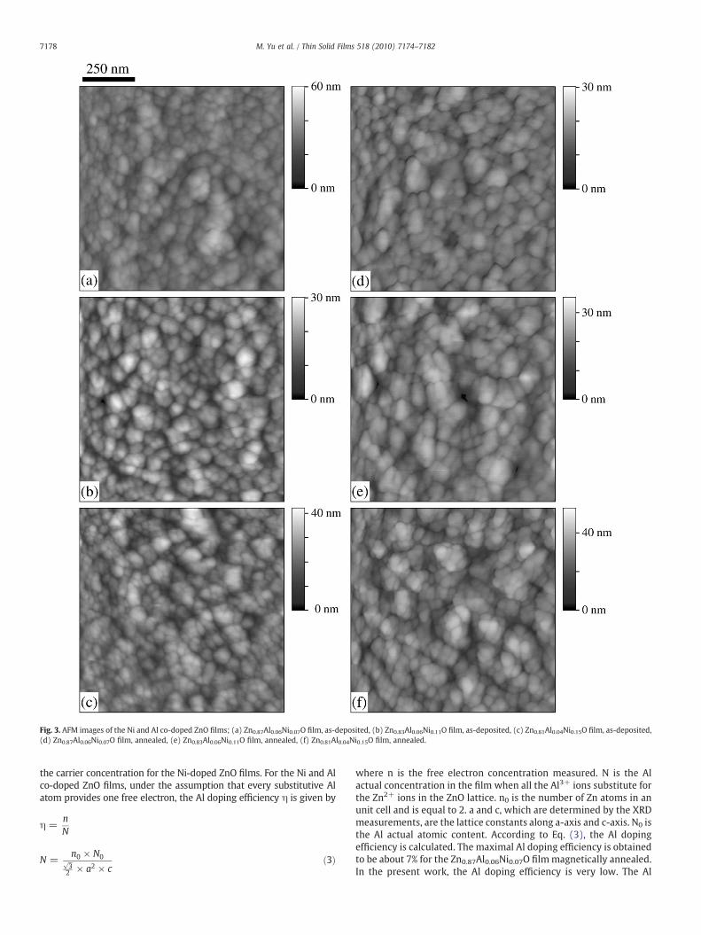
Fig. 3. AFM images of the Ni and Al co-doped ZnO films; (a) Zn0.87Al0.06Ni0.07O film, as-deposited, (b) Zn0.83Al0.06Ni0.11O film, as-deposited, (c) Zn0.81Al0.04Ni0.15O film, as-deposited,(d) Zn0.87Al0.06Ni0.07O film, annealed, (e) Zn0.83Al0.06Ni0.11O film, annealed, (f) Zn0.81Al0.04Ni0.15O film, annealed.
7178 M. Yu et al. / Thin Solid Films 518 (2010) 7174–7182
the carrier concentration for the Ni-doped ZnO films. For the Ni and Alco-doped ZnO films, under the assumption that every substitutive Alatom provides one free electron, the Al doping efficiency η is given by
η =nN
N =n0 × N0ffiffi3
p2 × a2 × c
ð3Þ
where n is the free electron concentration measured. N is the Alactual concentration in the film when all the Al3+ ions substitute forthe Zn2+ ions in the ZnO lattice. n0 is the number of Zn atoms in anunit cell and is equal to 2. a and c, which are determined by the XRDmeasurements, are the lattice constants along a-axis and c-axis. N0 isthe Al actual atomic content. According to Eq. (3), the Al dopingefficiency is calculated. The maximal Al doping efficiency is obtainedto be about 7% for the Zn0.87Al0.06Ni0.07O film magnetically annealed.In the present work, the Al doping efficiency is very low. The Al

Fig. 4.Magnetizition curves of the Ni and Al co-doped ZnO films; (a) Zn0.83Al0.06Ni0.11Ofilm, as-deposited, (b) Zn0.81Al0.04Ni0.15O film, as-deposited, (c) Zn0.87Al0.06Ni0.07O film,annealed, (d) Zn0.83Al0.06Ni0.11O film, annealed, (e) Zn0.81Al0.04Ni0.15O film, annealed.
Fig. 6. M–T curves of the Ni and Al co-doped ZnO films magnetically annealed.
7179M. Yu et al. / Thin Solid Films 518 (2010) 7174–7182
doping efficiency can be controlled by the competition of thesubstitution of Ni2+ and Al3+ ions for the Zn2+ ions. As the Nicontent in the films increases, many Ni2+ ions occupy the Zn2+ sites,leading to a decrease in the Al3+ ions substituting for the Zn2+ ions.Therefore, the high Ni content lowers the Al doping efficiency andthe free electron concentration in the Ni and Al co-doped ZnO films.Furthermore, the films growwith thin columnar grains. The Al atomsnot substituting for Zn2+ ions in the ZnO lattice can exist at the grainboundaries and don't play the donor role. On the other hand, for thefilms having the high Ni content, some Ni atoms could enter into theinterstitial sites of the ZnO lattice as indicated by the XRD results andpromote a formation of the defects with incomplete atomic bonds.The Ni interstitial atoms and the defects could form the scatteringcenters of free electrons. Therefore, for the as-deposited films theHall mobility decreases with increasing the Ni content. When thefilms were magnetically annealed, the crystallinity of the films isimproved as indicated by the AFM results and the Ni interstitialatoms aggregate promoting the growth of the Ni nano-clusters asindicated by the XRD results. The Ni nano-clusters could exist at thegrain boundaries. It is considered that the annealing decreases thedefects and the Ni interstitial atoms in the films, decreasing thescattering centers of free electrons. As a result, the annealing enhan-ces the Hall mobility in the Ni and Al co-doped ZnO films.
Fig. 5.Magnetizition curves of theNi andAl co-dopedZnOfilms annealedwithoutmagneticfield; (a) Zn0.87Al0.06Ni0.07O film, (b) Zn0.83Al0.06Ni0.11O film, (c) Zn0.81Al0.04Ni0.15O film.
Fig. 8 show a temperature dependence of the resistance for the Niand Al co-doped ZnO films as-deposited andmagnetically annealed. InFig. 8, the resistance RT at each temperature is normalized to theresistance R300K at 300 K. As can be seen from Fig. 8, the resistivity ofthe films decreases with increasing temperature. It exhibits asemiconducting behavior. For the Al-doped ZnO films, the Zninterstitial atoms, the O vacancies and the Al substitutive atoms inthe Zn lattice sites contribute to donors [25]. Generally, it isconsidered that Ni2+ ions substitute for the Zn2+ ions in the Ni-doped ZnO film [12,24] and the doping of Ni doesn't contribute to theincrease in the carrier concentration for the Ni-doped ZnO films.
The scattering mechanism of the carrier might mainly includeionized impurity scattering, grain boundary scattering and latticevibration scattering. The mean free path L of electrons in the films canbe given by [26]
L =h2e
� �3nπ
� �13
μ ð4Þ
where n is the free electron concentration and μ is the Hall mobility.h is the Planck constant and e is the elementary charge. Using the n

Fig. 7.Magnetization curves of the Ni and Al co-doped ZnO filmsmagnetically annealed.The magnetic field is applied parallel and perpendicular to the direction of theannealing magnetic field during the VSM measurements.
Fig. 8. Temperature dependence of the resistance for the Ni and Al co-doped ZnO films as-deposited and magnetically annealed. □: Zn0.87Al0.06Ni0.07O film, △: Zn0.83Al0.06Ni0.11Ofilm, ○: Zn0.81Al0.04Ni0.15O film.
7180 M. Yu et al. / Thin Solid Films 518 (2010) 7174–7182
and μ values obtained, themean free path of the electrons is estimatedto be significantly small relative to the grain size of the films.Therefore, in this case the grain boundary scattering might benegligible. The carrier mobility μI due to the ionized impurityscattering for a non-degenerate semiconductor is given by
μI∝T32 ð5Þ
and that μP due to the lattice vibration scattering is expressed as
μP∝T −32 ð6Þ
where T is the absolute temperature [27,28]. For the thermallyactivated band conduction, the free electron concentration n can begiven by [29]
n = NC exp −ΔEAkT
� �ð7Þ
where NC is a constant related to thematerial andΔEA is the activationenergy. k is the Boltzmann constant.
Table 3Electron concentrations n, Hall mobilities μ and resistivities ρ of the as-deposited andannealed films.
Film Treatment n (cm−3) μ (cm2/V s) ρ (Ω cm)
Zn0.87Al0.06Ni0.07O As-deposited 1.50×10²⁰ 2.70 1.54×10⁻²
Zn0.83Al0.06Ni0.11O As-deposited 2.4×10¹⁸ 0.20 15.5Zn0.81Al0.04Ni0.15O As-deposited 4.26×10¹⁸ 0.06 18.9Zn0.87Al0.06Ni0.07O Annealed 1.73×10²⁰ 4.16 8.73×10⁻³
Zn0.83Al0.06Ni0.11O Annealed 1.27×10²⁰ 3.18 1.6×10⁻²
Zn0.81Al0.04Ni0.15O Annealed 2.35×10¹⁸ 1.20 2.23
The resistivity is proportional to the reciprocal of the product ofcarrier concentration and Hall mobility. First, it is considered that thefree electronmobility is dominated by the ionized impurity scattering.Using Eqs. (5) and (7), the resistivity ρ of the film is expressed as
ρ∝T −32 exp
ΔEAkT
� �: ð8Þ
On the other hand, it was reported that the conductionmechanismdue to the thermal activation occurred at temperatures over 200 K forthe ZnO: Al films [30] and the ZnO films [28,31]. According to Eq. (8), avariation of ln(ρT3/2) with T−1 is plotted in Fig. 9. As can be seen fromFig. 9, for all the films, the plot over 200 K exhibits a well lineardependence. However, a negative activation energy is obtained interms of the slope of the straight line. It indicates that the ionizedimpurity scattering could not dominate the free electron transport inthe films. Then, using Eqs. (6) and (7), the resistivity ρ of the film isgiven by
ρ∝T32 exp
ΔEAkT
� �: ð9Þ
Fig. 10a shows a temperature dependence of the resistivity for theNi and Al co-doped ZnO films as-deposited and magneticallyannealed, plotted as ln(ρT−3/2) versus T−1. As can be seen fromFig. 10a, the plot can't exhibit the linear relationship in the wholemeasuring temperature range of 50–300 K, meaning that the freeelectron transport is not dominated by the single scattering mechanism.It is generally considered that the lattice vibration scattering ispredominant at the relatively high temperature. As shown in Fig. 10b, agood linear dependence having a linearity factor better than 0.995 isexhibited in the high temperature region. The activation energy iscalculated in terms of the slope of the fitted straight line. The activation

Fig. 9. Variation of ln(ρT3/2) with T−1 for the Ni and Al co-doped ZnO films.■: Zn0.87-Al0.06Ni0.07O film, as-deposited, ▲: Zn0.83Al0.06Ni0.11O film, as-deposited, ●: Zn0.81Al0.04-Ni0.15O film, as-deposited,□: Zn0.87Al0.06Ni0.07O film, annealed,△: Zn0.83Al0.06Ni0.11Ofilm, annealed, ○: Zn0.81Al0.04Ni0.15O film, annealed.
7181M. Yu et al. / Thin Solid Films 518 (2010) 7174–7182
energies for Zn0.87Al0.06Ni0.07O, Zn0.83Al0.06Ni0.11O and Zn0.81Al0.04Ni0.15Ofilms as-deposited are 36 meV, 56 meV and 65 meV while thosemagnetically annealed are 35 meV, 54 meV and 54meV, respectively.Considering the change in the free electron concentration, it can besaid that the activation energy for the thermally activated bandconduction depends on the carrier concentration and the impurityenergy level. An increase in the carrier concentration raises theFermi energy to a high level in the energy gap, leading to thedecrease in the activation energy [32]. For the low temperatureregion, the plot shown in Fig. 10a also exhibits a good linear
Fig. 10. Variation of ln(ρT− 3/2) with T− 1 for the Ni and Al co-doped ZnOfilms. ■: Zn0.87Al0.06Ni0.07O film, as-deposited, ▲: Zn0.83Al0.06Ni0.11O film, as-deposited,●: Zn0.81Al0.04Ni0.15O film, as-deposited, □: Zn0.87Al0.06Ni0.07O film, annealed,△: Zn0.83Al0.06Ni0.11O film, annealed, ○: Zn0.81Al0.04Ni0.15O film, annealed.
dependence. The fitted activation energies are lower than 9 meV andare very small. It means that a different carrier transport mechanism,i.e., not thermally activated band conduction, dominates at the lowtemperatures for the Ni and Al co-doped ZnO films.
At low temperatures the carrier transport mechanism can beexplained using the variable range hopping (VRH)model proposed byMott. The electrons hop between the localized states. These localizedstates exist inside the energy distribution region of the impurity levelin the energy gap. The electron hops from the occupied localized stateto the unoccupied one under the favourable condition. In the Mott'sVRH model, a relationship between the conductivity σ and thetemperature T is given by [28,30–32]
σ = σ0T−1
2 exp − T0T
� �14
" #ð10Þ
where σ0 and T0 are expressed as
σ0 =3e2νPffiffiffiffiffiffi
8πp ×
NðEFÞαkT
� �12 ð11Þ
T0 =16α3
kNðEFÞð12Þ
where νP is the phonon frequency (≈1013 Hz) at Debye temperature.N(EF) is the density of the localized electron states at Fermi level. α isthe inverse localization length of wave function associated with thelocalized state. Fig. 11 shows a temperature dependence of theconductivity for the Ni and Al co-doped ZnO films as-deposited andmagnetically annealed, plotted as ln(σT1/2) versus T−1/4. As can beseen from Fig. 11, the plot can't exhibit the linear relationship in thewhole measuring temperature range of 50–300 K. However, itexhibits a good linear dependence having a linearity factor of 0.998in the low temperature range. According to Eq. (10), the T0 value iscalculated in terms of the slope of the fitted straight line and the σ0
value is obtained by the intercept of the fitted line and the ln(σT1/2)axis. The T0 and σ0 values are summarized in Table 4. Using Eqs. (11)and (12), N(EF) and α are calculated and also listed in Table 4. Asshown in Table 4, the as-deposited Zn0.87Al0.06Ni0.07O film as well asthe Zn0.87Al0.06Ni0.07O and Zn0.83Al0.06Ni0.11O films magneticallyannealed have the high density of the localized electron state andthe narrow localization length of the wave function. For the Ni and Alco-doped ZnO films, the high crystallinity results in the high density ofthe localized state and the narrow localization length of the wave
Fig. 11. Variation of ln(σT1/2) with T− 1/4 for the Ni and Al co-doped ZnOfilms. ■: Zn0.87Al0.06Ni0.07O film, as-deposited, ▲: Zn0.83Al0.06Ni0.11O film, as-deposited, ●: Zn0.81Al0.04Ni0.15O film, as-deposited, □: Zn0.87Al0.06Ni0.07O film,annealed,△: Zn0.83Al0.06Ni0.11O film, annealed, ○: Zn0.81Al0.04Ni0.15O film, annealed.
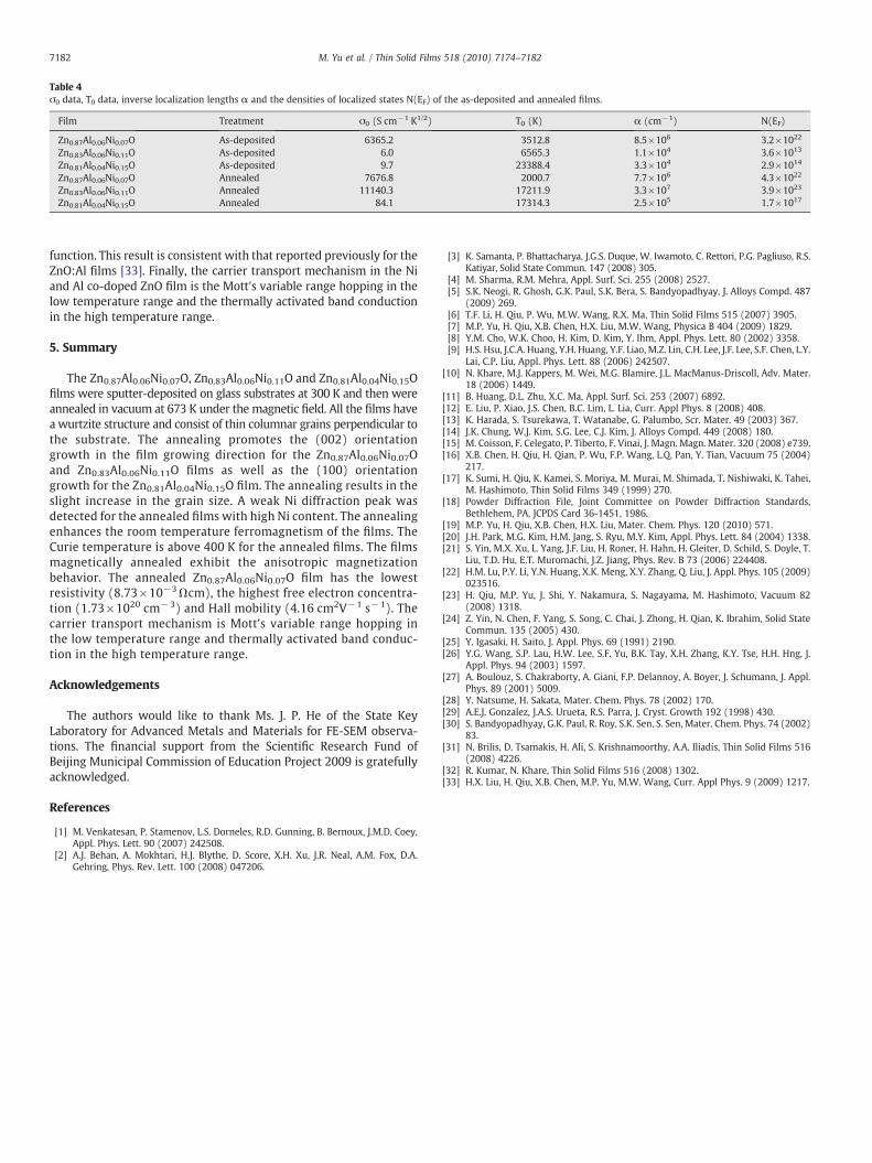
Table 4σ0 data, T0 data, inverse localization lengths α and the densities of localized states N(EF) of the as-deposited and annealed films.
Film Treatment σ0 (S cm−1 K1/2) T0 (K) α (cm−1) N(EF)
Zn0.87Al0.06Ni0.07O As-deposited 6365.2 3512.8 8.5×10⁶ 3.2×10²²
Zn0.83Al0.06Ni0.11O As-deposited 6.0 6565.3 1.1×10⁴ 3.6×10¹³
Zn0.81Al0.04Ni0.15O As-deposited 9.7 23388.4 3.3×10⁴ 2.9×10¹⁴
Zn0.87Al0.06Ni0.07O Annealed 7676.8 2000.7 7.7×10⁶ 4.3×10²²
Zn0.83Al0.06Ni0.11O Annealed 11140.3 17211.9 3.3×10⁷ 3.9×10²³
Zn0.81Al0.04Ni0.15O Annealed 84.1 17314.3 2.5×10⁵ 1.7×10¹⁷
7182 M. Yu et al. / Thin Solid Films 518 (2010) 7174–7182
function. This result is consistent with that reported previously for theZnO:Al films [33]. Finally, the carrier transport mechanism in the Niand Al co-doped ZnO film is the Mott's variable range hopping in thelow temperature range and the thermally activated band conductionin the high temperature range.
5. Summary
The Zn0.87Al0.06Ni0.07O, Zn0.83Al0.06Ni0.11O and Zn0.81Al0.04Ni0.15Ofilms were sputter-deposited on glass substrates at 300 K and then wereannealed in vacuum at 673 K under the magnetic field. All the films havea wurtzite structure and consist of thin columnar grains perpendicular tothe substrate. The annealing promotes the (002) orientationgrowth in the film growing direction for the Zn0.87Al0.06Ni0.07Oand Zn0.83Al0.06Ni0.11O films as well as the (100) orientationgrowth for the Zn0.81Al0.04Ni0.15O film. The annealing results in theslight increase in the grain size. A weak Ni diffraction peak wasdetected for the annealed films with high Ni content. The annealingenhances the room temperature ferromagnetism of the films. TheCurie temperature is above 400 K for the annealed films. The filmsmagnetically annealed exhibit the anisotropic magnetizationbehavior. The annealed Zn0.87Al0.06Ni0.07O film has the lowestresistivity (8.73×10⁻³Ωcm), the highest free electron concentra-tion (1.73×1020 cm−3) and Hall mobility (4.16 cm2V−1 s−1). Thecarrier transport mechanism is Mott's variable range hopping inthe low temperature range and thermally activated band conduc-tion in the high temperature range.
Acknowledgements
The authors would like to thank Ms. J. P. He of the State KeyLaboratory for Advanced Metals and Materials for FE-SEM observa-tions. The financial support from the Scientific Research Fund ofBeijing Municipal Commission of Education Project 2009 is gratefullyacknowledged.
References
[1] M. Venkatesan, P. Stamenov, L.S. Dorneles, R.D. Gunning, B. Bernoux, J.M.D. Coey,Appl. Phys. Lett. 90 (2007) 242508.
[2] A.J. Behan, A. Mokhtari, H.J. Blythe, D. Score, X.H. Xu, J.R. Neal, A.M. Fox, D.A.Gehring, Phys. Rev. Lett. 100 (2008) 047206.
[3] K. Samanta, P. Bhattacharya, J.G.S. Duque, W. Iwamoto, C. Rettori, P.G. Pagliuso, R.S.Katiyar, Solid State Commun. 147 (2008) 305.
[4] M. Sharma, R.M. Mehra, Appl. Surf. Sci. 255 (2008) 2527.[5] S.K. Neogi, R. Ghosh, G.K. Paul, S.K. Bera, S. Bandyopadhyay, J. Alloys Compd. 487
(2009) 269.[6] T.F. Li, H. Qiu, P. Wu, M.W. Wang, R.X. Ma, Thin Solid Films 515 (2007) 3905.[7] M.P. Yu, H. Qiu, X.B. Chen, H.X. Liu, M.W. Wang, Physica B 404 (2009) 1829.[8] Y.M. Cho, W.K. Choo, H. Kim, D. Kim, Y. Ihm, Appl. Phys. Lett. 80 (2002) 3358.[9] H.S. Hsu, J.C.A. Huang, Y.H. Huang, Y.F. Liao, M.Z. Lin, C.H. Lee, J.F. Lee, S.F. Chen, L.Y.
Lai, C.P. Liu, Appl. Phys. Lett. 88 (2006) 242507.[10] N. Khare, M.J. Kappers, M. Wei, M.G. Blamire, J.L. MacManus-Driscoll, Adv. Mater.
18 (2006) 1449.[11] B. Huang, D.L. Zhu, X.C. Ma, Appl. Surf. Sci. 253 (2007) 6892.[12] E. Liu, P. Xiao, J.S. Chen, B.C. Lim, L. Lia, Curr. Appl Phys. 8 (2008) 408.[13] K. Harada, S. Tsurekawa, T. Watanabe, G. Palumbo, Scr. Mater. 49 (2003) 367.[14] J.K. Chung, W.J. Kim, S.G. Lee, C.J. Kim, J. Alloys Compd. 449 (2008) 180.[15] M. Coisson, F. Celegato, P. Tiberto, F. Vinai, J. Magn. Magn. Mater. 320 (2008) e739.[16] X.B. Chen, H. Qiu, H. Qian, P. Wu, F.P. Wang, L.Q. Pan, Y. Tian, Vacuum 75 (2004)
217.[17] K. Sumi, H. Qiu, K. Kamei, S. Moriya, M. Murai, M. Shimada, T. Nishiwaki, K. Tahei,
M. Hashimoto, Thin Solid Films 349 (1999) 270.[18] Powder Diffraction File, Joint Committee on Powder Diffraction Standards,
Bethlehem, PA, JCPDS Card 36-1451, 1986.[19] M.P. Yu, H. Qiu, X.B. Chen, H.X. Liu, Mater. Chem. Phys. 120 (2010) 571.[20] J.H. Park, M.G. Kim, H.M. Jang, S. Ryu, M.Y. Kim, Appl. Phys. Lett. 84 (2004) 1338.[21] S. Yin, M.X. Xu, L. Yang, J.F. Liu, H. Roner, H. Hahn, H. Gleiter, D. Schild, S. Doyle, T.
Liu, T.D. Hu, E.T. Muromachi, J.Z. Jiang, Phys. Rev. B 73 (2006) 224408.[22] H.M. Lu, P.Y. Li, Y.N. Huang, X.K. Meng, X.Y. Zhang, Q. Liu, J. Appl. Phys. 105 (2009)
023516.[23] H. Qiu, M.P. Yu, J. Shi, Y. Nakamura, S. Nagayama, M. Hashimoto, Vacuum 82
(2008) 1318.[24] Z. Yin, N. Chen, F. Yang, S. Song, C. Chai, J. Zhong, H. Qian, K. Ibrahim, Solid State
Commun. 135 (2005) 430.[25] Y. Igasaki, H. Saito, J. Appl. Phys. 69 (1991) 2190.[26] Y.G. Wang, S.P. Lau, H.W. Lee, S.F. Yu, B.K. Tay, X.H. Zhang, K.Y. Tse, H.H. Hng, J.
Appl. Phys. 94 (2003) 1597.[27] A. Boulouz, S. Chakraborty, A. Giani, F.P. Delannoy, A. Boyer, J. Schumann, J. Appl.
Phys. 89 (2001) 5009.[28] Y. Natsume, H. Sakata, Mater. Chem. Phys. 78 (2002) 170.[29] A.E.J. Gonzalez, J.A.S. Urueta, R.S. Parra, J. Cryst. Growth 192 (1998) 430.[30] S. Bandyopadhyay, G.K. Paul, R. Roy, S.K. Sen, S. Sen, Mater. Chem. Phys. 74 (2002)
83.[31] Ν. Brilis, D. Tsamakis, H. Ali, S. Krishnamoorthy, A.A. Iliadis, Thin Solid Films 516
(2008) 4226.[32] R. Kumar, N. Khare, Thin Solid Films 516 (2008) 1302.[33] H.X. Liu, H. Qiu, X.B. Chen, M.P. Yu, M.W. Wang, Curr. Appl Phys. 9 (2009) 1217.