
Preliminary BMS design and sensor integration concept
35
Delivering the 3b g e neration of L NMO cells for the x EV mark e t of 2025 and beyond Preliminary BMS design and sensor integration concept Horizon 2020 | LC-BAT-5-2019 Research and innovation for advanced Li-ion cells (generation 3b) GA # 875033 Deliverable No. D4.1 Deliverable Title Preliminary BMS design and sensor integration concept Due Date 2020-04-30 Deliverable Type Report Dissemination level Public Written By Stefan Waldhör (FhG) 2021-04-30 Checked by Simone Mannori (ENEA) 2021-04-24 Approved by Claudio Lanciotti (MIT), Boschidar Ganev (AIT) 2021-04-29 Status Final 2021-04-30 This project has received funding from the European Union’s H2020 research and innovation programme under Grant Agreement no. 875033. This publication reflects only the author’s view and the Innovation and Networks Executive Agency (INEA) is not responsible for any use that may be made of the information it contains. Ref. Ares(2021)2904016 - 30/04/2021
Transcript of Preliminary BMS design and sensor integration concept

Delivering the 3b generation of LNMO cells for the xEV market of 2025 and beyond
Preliminary BMS design and sensor integration concept
Horizon 2020 | LC-BAT-5-2019 Research and innovation for advanced Li-ion cells (generation 3b)
GA # 875033
Deliverable No. D4.1
Deliverable Title Preliminary BMS design and sensor integration concept
Due Date 2020-04-30
Deliverable Type Report
Dissemination level Public
Written By Stefan Waldhör (FhG) 2021-04-30
Checked by Simone Mannori (ENEA) 2021-04-24
Approved by Claudio Lanciotti (MIT), Boschidar Ganev (AIT) 2021-04-29
Status Final 2021-04-30
This project has received funding from the European Union’s H2020 research and innovation programme under Grant Agreement no. 875033. This publication reflects only the author’s view and the Innovation and Networks Executive Agency (INEA) is not responsible for any use that may be made of the information it contains.
Ref. Ares(2021)2904016 - 30/04/2021

Revision History
Version Date Who Changes
1.1 2021-04-30 AIT • Reviewed final version of the document
1.0 2021-04-28 FhG • Final version of the document
0.14 2021-04-28 MIT • Review of the document
0.13 2021-04-21 FHG • Add conclusion
0.12 2021-04-21 VALEO • Add section on mechanical integration
• Add section on thermal management system
0.11 2021-04-19 FhG
• Add image of foxBMS 2 Master Unit
• Add paragraph on foxBMS 2 Master Unit
• Update system architecture block diagram with TMB
• Add section on the Interface Board
• Add section on data storage and connectivity
• Add section on mechanical integration
0.10 2021-03-17 FhG • Fix figure references
• Add paragraph on BMS communication
0.9 2021-03-17 ABEE • Add Operating Strategies
0.8 2021-03-12 Insplorion • Add details on the Insplorion sensor board
0.7 2021-03-08 FhG • Fix formatting
• Fix typos
0.6 2021-03-08 NXP • Add details on the NXP monitoring IC
0.5 2021-03-03 FhG • Update module and communication figures
0.4 2021-03-03 SENSICHIPS • Add details on the Sensichips Sensor
0.3 2021-03-01 FhG • Add details on hardware and software
0.2 2021-02-04 FhG • Add document structure and overview
0.1 2021-02-04 FhG • Initial version of the document

3beLiEVe | D4.1 – Preliminary BMS design and sensor integration concept
1
Project Abstract 3beLiEVe aims to strengthen the position of the European battery and automotive industry in the future xEV
market by delivering the next generation of battery cells, designed and made in Europe, for the electrified
vehicles market of 2025 and beyond. The project activities are focused on three domains:
• Development of automotive battery cells that are highly performant (high energy density, fast charge capability, long cycle life) and free of critical raw materials such as cobalt and natural graphite;
• Development and integration of sensors into and onto the cells to enable smart, adaptive operating strategies and advanced diagnostics in order to extend the useful life of the battery in first and second life applications and improve safety;
• A comprehensive manufacturing approach that is designed from the outset for a circular economy and industrial volumes. This encompasses green manufacturing processes for cell, module and pack, as well as recyclability assessment of the components, and a target lifecycle cost of 90 €/kWh at scale.
The project will deliver two 12kWh-demonstrator battery packs at TRL6 and MRL8. These aim at
demonstrating the 3beLiEVe technology performance for applications in light duty (i.e. passenger cars, freight
vehicles) and commercial vehicles (i.e. city buses and trucks) in fully electric/plug-in hybrid (BEV/PHEV)
configurations.
The strong and complementary consortium of 21 partners from 10 different European countries representing
industrial companies, SMEs, RTOs and academia is coordinated by AIT Austrian Institute of Technology.
3beLiEVe is scheduled to run from January 1st, 2020 to June 30th, 2023, for a total duration of 42 months
and has received funding from the European Union’s H2020 research and innovation programme under Grant
Agreement no. 875033. A full list of partners and funding can be found at:
https://cordis.europa.eu/project/id/875033.
Figure 1: Overview of major 3beLiEVe project steps

3beLiEVe | D4.1 – Preliminary BMS design and sensor integration concept
2
Executive Summary One key component of the success of battery electric mobility and renewable energy usage is the safe and
reliable usage of the battery system within the application, e.g. battery electric vehicle (BEV) or Battery
Energy Storage System (BESS). Furthermore, the performance and durability of the system must fulfil the
market and consumer expectations when using the battery-powered application. The safety of the battery
system currently mostly relies on voltage, current and temperature measurement. The performance is
specified at the beginning of life of the battery system. 3beLiEVe implements innovative sensors such as
Surface Plasmon Resonance (SPR), Electrochemical Impedance Spectroscopy (EIS) and gas sensors in
combination with well-established and safety-certified voltage and temperature measurement on the second
generation of the open-source Battery Management System (BMS) foxBMS. Innovative operating strategies
are developed on a modelling base that combine traditional with new modelling techniques such as Artificial
Intelligence. Additionally, the BMS implements safety functionalities like a System Basis Chip (SBC) and new
operating strategies for battery electric applications. The foxBMS software and hardware documentation are
made publicly available to empower everybody to develop beyond state-of-the-art battery management
systems with safety in mind.
This document gives an overview about the BMS, the sensors, the overall integration and the operating
strategies that will be developed. The integration consists of the communication integration of all sensor
components with the BMS and the mechanical integration in the battery pack.

3beLiEVe | D4.1 – Preliminary BMS design and sensor integration concept
3
Table of Contents
Revision History ................................................................................................................................................. 0
Table of Contents .............................................................................................................................................. 3
1. Introduction ............................................................................................................................................... 7
1.1. Battery Management System foxBMS............................................................................................... 7
1.2. Pack and Module Design ................................................................................................................... 7
2. Sensors and Actuators ............................................................................................................................. 11
2.1. Insplorion Fibre Optical Surface Plasmon Resonance Sensor ......................................................... 11
2.2. Sensichips’ Cell Management Unit (CMU) and the SENSIPLUS IC ................................................... 13
2.3. NXP MC33775A IC ........................................................................................................................... 14
2.3.1. Cell Terminal Measurement .................................................................................................... 15
2.3.2. GPIOs ....................................................................................................................................... 15
2.4. Valeo Thermal Management System .............................................................................................. 16
3. Battery Management System .................................................................................................................. 18
3.1. Overview .......................................................................................................................................... 18
3.1.1. Hardware ................................................................................................................................. 18
3.1.2. Software .................................................................................................................................. 19
3.2. Boards .............................................................................................................................................. 21
3.2.1. Master Unit .............................................................................................................................. 21
3.2.2. Interface Board ........................................................................................................................ 24
3.2.3. Slaves Units .............................................................................................................................. 25
3.2.4. Data Storage and Communication........................................................................................... 26
3.3. Operating Strategies ........................................................................................................................ 26
4. Mechanical Integration............................................................................................................................ 30
5. Conclusions .............................................................................................................................................. 31
References ......................................................................................................................................................... 32
3beLiEVe | D4.1 – Preliminary BMS design and sensor integration concept
4
List of figure and tables Figure 1: Overview of major 3beLiEVe project steps ........................................................................................ 1 Figure 2: Battery Pack Architecture 100 V (Demonstrator 1) ........................................................................... 8 Figure 3: Battery Pack Architecture 200 V (Demonstrator 2) ........................................................................... 9 Figure 4: Module architecture. “TPL” double arrows at the top left and top right of the diagram indicate TPL bus connections to other modules. See also Figure 14. .................................................................................. 10 Figure 5: Insplorion FOS Architecture ............................................................................................................. 12 Figure 6: Dimensions of the Insplorion FOSPR electronics ............................................................................. 12 Figure 7: SENSIPLUS internal functional Block Diagram .................................................................................. 13 Figure 8: NXP MC33775A Architecture ........................................................................................................... 14 Figure 9: Temperature measurement ............................................................................................................. 15 Figure 10: I2C Bus ............................................................................................................................................ 16 Figure 11: Coolant flow ................................................................................................................................... 16 Figure 12: Block diagram of the coolant flow .................................................................................................. 17 Figure 13: foxBMS 2 Master Unit architecture ................................................................................................ 18 Figure 14: foxBMS 2 communication between Master Unit and Slave Units and the thermal management system board (TBM) ........................................................................................................................................ 19 Figure 15: foxBMS 2 Software Architecture .................................................................................................... 20 Figure 16: foxBMS 2 embedded software stack .............................................................................................. 21 Figure 17: foxBMS 2 Master Unit .................................................................................................................... 22 Figure 18: Block diagram of the foxBMS 2 master .......................................................................................... 23 Figure 19: Detail description of an isolated CAN-interface ............................................................................. 24 Figure 20: foxBMS 2 communication buses .................................................................................................... 24 Figure 21: foxBMS 2 Slave Unit ....................................................................................................................... 26 Figure 22: Proposed operating strategy by ABEE ............................................................................................ 27 Figure 23: A fuzzy PID controller for each module .......................................................................................... 28 Figure 24: Distribution of membership functions for input variable (e(k)) ..................................................... 28 Figure 25: Proposed architecture for SOX estimation ..................................................................................... 29 Figure 26: Module design ................................................................................................................................ 30 Figure 27: Design space for the foxBMS 2 NXP slave board ............................................................................ 31

3beLiEVe | D4.1 – Preliminary BMS design and sensor integration concept
5
List of abbreviations Acronym / Short Name Meaning
ADC Analog to Digital Converter
AI Artificial Intelligence
AOSE Analog Output Single Ended
AUX Auxiliary
(B)ESS (Battery) Energy Storage System
BEV Battery Electric Vehicle
BIST Built-In Self-Test
BMS Battery Management System
CAN Controller Area Network, a bus standard
CIC Cascaded Integrated Comb filter
CRM Critical Raw Materials
CMU Cell Management Unit
DAC Digital to Analog Converter
DAS Direct Analog Synthesis
DMA Direct Memory Access
DDS Direct Digital Synthesis
ECC Error correction code
EIS Electrical Impedance Spectroscopy
EKF Extended Kalman Filter
ESS Energy Storage Systems
EV Electric Vehicles
FIFO First In First Out
FOSPR Fibre Optical Surface Plasmon Resonance
FRAM Ferroelectric random-access memory
GPIO General Purpose Input/Output
HAL Hardware Abstraction Layer
HEV Hybrid Electric Vehicle
IC Integrated Circuit
I2C Inter-Integrated Circuit, a serial communication bus
I3C MIPI I3C simple serial interface
INT Interrupt
IoT Internet of Things
LDO Low-dropout regulator
LDO Low Dropout regulator
MEMS Microelectromechanical system
MTBF Mean time between failure
OSC Oscillator
OTP One Time Programmable
PCB Printed Circuit Board
PID Proportional-Integral-Derivative
3beLiEVe | D4.1 – Preliminary BMS design and sensor integration concept
6
POR Power On Reset
POT Potentiostat
QSPI Queued Serial Peripheral Interface
RH Relative Humidity sensor
RMS Root mean square
SBC System Basis Chip
SLM SENSIPLUS Learning Machine
SOC State of Charge
SOH State of Health
SOX State of X, where X can be e.g., Charge, Health
SPI Serial Peripheral Interface
SPI Serial Peripheral Interface
SPR Surface Plasmon Resonance
SPS Smart Power Switch
SRAM Static random-access memory
TLBO Teaching-Learning-Based Optimization
TPL Transformer Physical Layer (bus developed by NXP)
UPS Uninterruptible power supply
VCSEL Vertical-cavity surface-emitting laser
VOC Volatile Organic Compounds

3beLiEVe | D4.1 – Preliminary BMS design and sensor integration concept
7
1. Introduction The overall approach of the battery system and its target application must be considered when adapting and
extending the Battery Management System (BMS). In the case of 3beLiEVe, the target applications are for
automotive use.
Section 1 provides the rationale behind the development of foxBMS2 and a short introduction on the high-
level battery system design and the demonstrators that are developed in the 3beLiEVe project. Section 2
describes the sensors that will provide data input to the BMS. Section 3 then describes the BMS itself in detail
and gives a first overview of the operating strategies that it will employ in order to control vital functions of
the battery module and pack, such as charge, discharge, cooling, and state of safety. Section 4 describes the
mechanical integration of the previously described components into the module.
1.1. Battery Management System foxBMS
Developing a BMS from the ground up is a time-consuming and repetitive task. To overcome this drawback
in many research, development and rapid-prototyping projects, Fraunhofer IISB has developed the open
source BMS “foxBMS” and made it publicly available in 2016 [1]. The BMS in project 3beLiEVe is based on the
newly-developed second generation of foxBMS called foxBMS 2. The first development version of foxBMS 2
has been publicly available since April 2021 [2]. foxBMS 2 is released under very permissive open source
licenses. The software is covered by the BSD 3-Clause License and the hardware and documentation by the
Creative Commons Attribution 4.0 International License. These licenses allow and encourage everybody to
review and verify the implementations and furthermore empower everybody to build beyond state-of-the-
art battery management systems based on software and hardware that does not compromise the outcomes
with restricted licenses and does not create a vendor lock-in. This is beneficial for research purposes as well
as for industry.
1.2. Pack and Module Design
The battery pack demonstrator in 3beLiEVe is based on an 8s1p1 module architecture. The number of eight
cells per module has been selected based on the best compromise with the envisaged cooling system. This
module structure allows for approximately 36 V of nominal voltage using the 3b generation LMNO pouch
cells developed by Custom Cells Itzehoe. Thus, three modules in series are needed to achieve a nominal
voltage of 100 V in the first demonstrator pack and six modules for the nominal voltage of 200 V in the second
demonstrator pack.
Based on the target 30 Ah / 135 Wh pouch cell format, each module has a capacity of 30 Ah and an energy
content of 1.1 kWh.
• The 3beLiEVe battery demonstrator at 100 V will consist of four parallel strings of three modules
each, for a total energy content of 13 kWh with 96 cells.
• The 3beLiEVe battery demonstrator at 200 V will consist of two parallel strings of six modules each,
for the same capacity and cell count. These configurations are considered the most beneficial for the
objectives of the project.
1 8s1p: 8 cells in series and no cell parallelisation inside a module
3beLiEVe | D4.1 – Preliminary BMS design and sensor integration concept
8
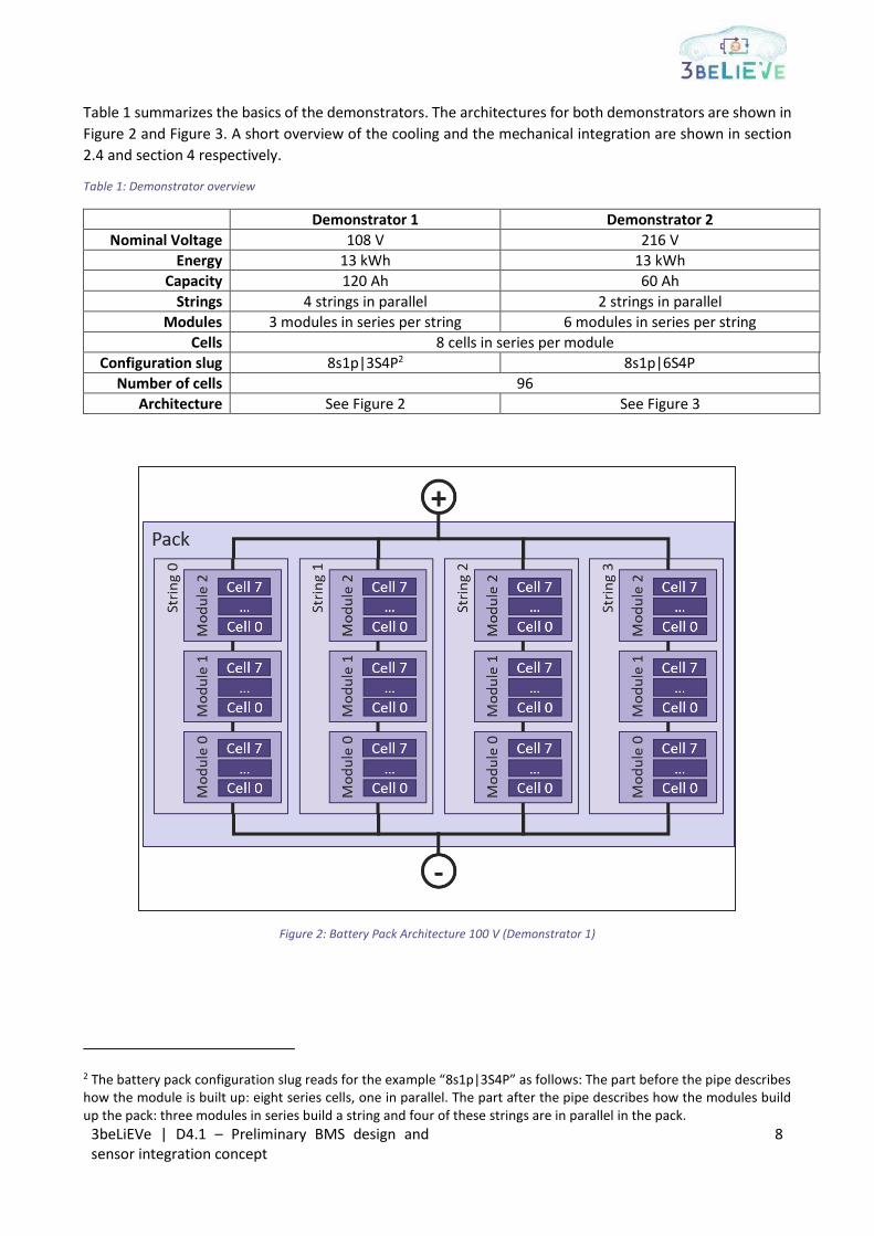
Table 1 summarizes the basics of the demonstrators. The architectures for both demonstrators are shown in
Figure 2 and Figure 3. A short overview of the cooling and the mechanical integration are shown in section
2.4 and section 4 respectively.
Table 1: Demonstrator overview
Demonstrator 1 Demonstrator 2
Nominal Voltage 108 V 216 V
Energy 13 kWh 13 kWh
Capacity 120 Ah 60 Ah
Strings 4 strings in parallel 2 strings in parallel
Modules 3 modules in series per string 6 modules in series per string
Cells 8 cells in series per module
Configuration slug 8s1p|3S4P2 8s1p|6S4P
Number of cells 96
Architecture See Figure 2 See Figure 3
Figure 2: Battery Pack Architecture 100 V (Demonstrator 1)
2 The battery pack configuration slug reads for the example “8s1p|3S4P” as follows: The part before the pipe describes how the module is built up: eight series cells, one in parallel. The part after the pipe describes how the modules build up the pack: three modules in series build a string and four of these strings are in parallel in the pack.
3beLiEVe | D4.1 – Preliminary BMS design and sensor integration concept
9
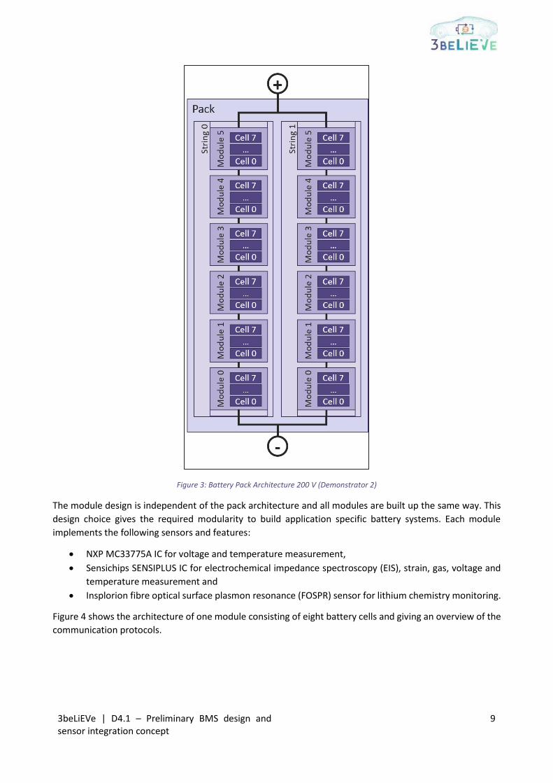
Figure 3: Battery Pack Architecture 200 V (Demonstrator 2)
The module design is independent of the pack architecture and all modules are built up the same way. This
design choice gives the required modularity to build application specific battery systems. Each module
implements the following sensors and features:
• NXP MC33775A IC for voltage and temperature measurement,
• Sensichips SENSIPLUS IC for electrochemical impedance spectroscopy (EIS), strain, gas, voltage and
temperature measurement and
• Insplorion fibre optical surface plasmon resonance (FOSPR) sensor for lithium chemistry monitoring.
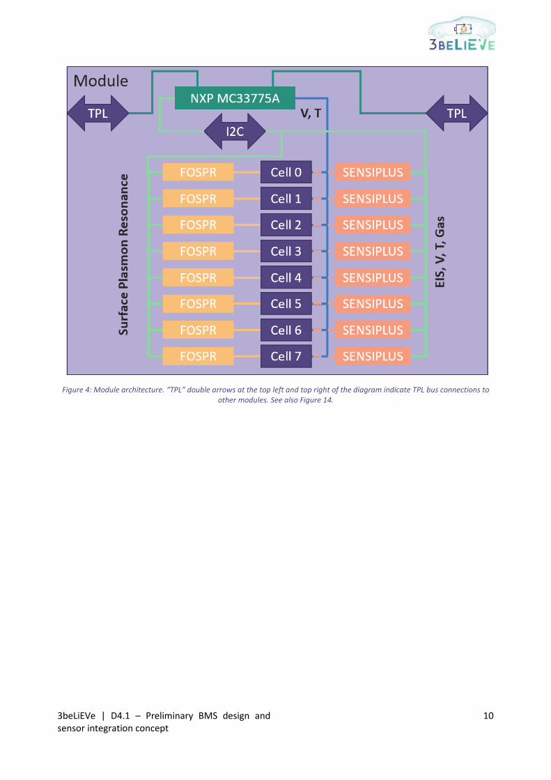
Figure 4 shows the architecture of one module consisting of eight battery cells and giving an overview of the
communication protocols.
3beLiEVe | D4.1 – Preliminary BMS design and sensor integration concept
10
Figure 4: Module architecture. “TPL” double arrows at the top left and top right of the diagram indicate TPL bus connections to other modules. See also Figure 14.

3beLiEVe | D4.1 – Preliminary BMS design and sensor integration concept
11
2. Sensors and Actuators The following sections give an overview of the capability of the measurement ICs and external sensors and
actuators connected to the foxBMS 2 Master Unit:
• NXP MC33664/MC33775A: cell voltage and temperature measurement and cell balancing
• Insplorion FOSPR-sensor: opto-electronic sensor for lithium chemistry monitoring
• Sensichips’ SENSIPLUS: internal cell impedance spectra, cell swelling, out-gassing, electrolyte
leakage, cell voltage and temperature
• Valeo Thermal Management System Board (TMB): sensor for cooling fluid temperature
measurement and valve control for flow control.
2.1. Insplorion Fibre Optical Surface Plasmon Resonance Sensor
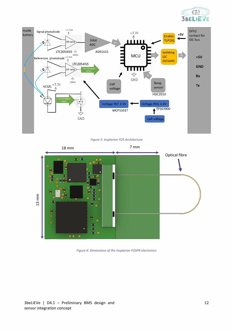
Insplorion utilizes an optical sensor that is placed between the separator and one of the electrodes inside battery cells. It has a nano sensing structure sensitive to chemical and structural changes in the materials close to the sensor. The sensor structure is placed on a 100 μm diameter optical fibre. This sensor is looped inside the battery cell so that the two ends enter and exit approximately 10 mm apart in the same seal, at one end of the pouch. Readout of the sensor signal requires that light be shone into the fibre using a photodiode and that the light transmitted through the sensor is measured using a photodiode. The obtained signal is a change in the transmitted light intensity. The two main challenges for Insplorion in the 3beLiEVe project are to miniaturize the sensor board to a size that does not obstruct the modular pack design, and to find a design that allows the fibre to enter and exit the cell without compromising the cell integrity nor cause risk of fibre damage. This has led Insplorion to develop a separate fibre coupling PCB with the light source, reference diode and signal diode wire bonded to minimize the size required for the “fibre coupling”. Close collaboration with Custom Cells Itzehoe and Valeo has been an important activity during this development.
The electronic circuit is built around the commercial Atmega328PB microcontroller that handles the internal communication and control signals on the sensor board. It also handles the communication as an I2C slave on the daisy chaining sensor configuration. The electronics in the Insplorion sensor have one analog and one digital section. The analog section is located at each end of the fibre. On one side the circuit regulates the intensity of the light source (a Vertical Cavity Surface Emitting Laser, VCSEL). This is performed to ensure a stable optical readout signal unperturbed by exterior factors, such as temperature induced drift and aging effects. On the other side of the fibre the optical signal is detected by a photodiode, amplified and A/D converted. The digital circuit centred around the Atmega328PB handles communications with the analog to digital IC and an on-board temperature sensor.
The Insplorion sensor board is powered by the battery cell it is measuring. A commercial voltage regulator from Texas instruments is used (TPS63900) to achieve an output of 3.3V. To ensure that cell discharging is limited when the sensors are not in use the voltage regulator can be disabled by the microprocessor and turn itself off. The current drawn in the off state is below 100nA. The sensor is reenabled via the I2C bus. This sensor board is also equipped with the commercial ISO1640 IC, a high voltage digital bus isolator from Texas Instruments. It is AEC-Q100 qualified and with up to 3000 VRMS isolation rating and up to 5 kV surge capability. Figure 5 shows the architecture of the sensor and Figure 6 show the rendering of the PCB design.
3beLiEVe | D4.1 – Preliminary BMS design and sensor integration concept
12
Figure 5: Insplorion FOS Architecture
Figure 6: Dimensions of the Insplorion FOSPR electronics
Optical fibre
18 mm 7 mm
13
mm
3beLiEVe | D4.1 – Preliminary BMS design and sensor integration concept
13
2.2. Sensichips’ Cell Management Unit (CMU) and the SENSIPLUS IC
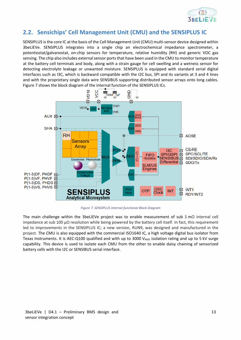
SENSIPLUS is the core IC at the basis of the Cell Management Unit (CMU) multi-sensor device designed within 3beLiEVe. SENSIPLUS integrates into a single chip an electrochemical impedance spectrometer, a potentiostat/galvanostat, on-chip sensors for temperature, relative humidity (RH) and generic VOC gas sensing. The chip also includes external sensor ports that have been used in the CMU to monitor temperature at the battery cell terminals and body, along with a strain gauge for cell swelling and a wetness sensor for detecting electrolyte leakage or unwanted moisture. SENSIPLUS is equipped with standard serial digital interfaces such as I3C, which is backward compatible with the I2C bus, SPI and its variants at 3 and 4 lines and with the proprietary single data wire SENSIBUS supporting distributed sensor arrays onto long cables. Figure 7 shows the block diagram of the internal function of the SENSIPLUS ICs.
Figure 7: SENSIPLUS internal functional Block Diagram
The main challenge within the 3beLiEVe project was to enable measurement of sub 1 mΩ internal cell impedance at sub 100 μΩ resolution while being powered by the battery cell itself. In fact, this requirement led to improvements in the SENSIPLUS IC; a new version, RUN9, was designed and manufactured in the project. The CMU is also equipped with the commercial ISO1640 IC, a high voltage digital bus isolator from Texas Instruments. It is AEC-Q100 qualified and with up to 3000 VRMS isolation rating and up to 5 kV surge capability. This device is used to isolate each CMU from the other to enable daisy chaining of sensorized battery cells with the I2C or SENSIBUS serial interface.

3beLiEVe | D4.1 – Preliminary BMS design and sensor integration concept
14
2.3. NXP MC33775A IC
The MC33775A is a lithium-ion battery cell controller IC designed for automotive applications, such as hybrid
electric (HEV) and battery electric vehicles (BEV). It can be used in industrial applications, such as energy
storage systems (ESS) and uninterruptible power supply (UPS) systems. The device performs high precision
ADC conversions of the differential cell voltages and battery temperatures. The measurements are
transmitted through SPI or an isolated daisy chain to a microcontroller for processing. The MC33775A offers
increased safety level and a low bill of materials. Figure 8 shows the architecture of the NXP MC33775A IC.
Figure 8: NXP MC33775A Architecture

3beLiEVe | D4.1 – Preliminary BMS design and sensor integration concept
15
2.3.1. Cell Terminal Measurement
The MC33775A offers a primary and a secondary measurement chain. The two chains are independent from
each other. The event-handling block monitors the synchronicity between the primary and secondary
measurements. The MC33775A allows four main measurement modes:
• Periodic measurements
• Application timed continuous measurements
• Synchronized measurements of cell voltage and voltage balancing terminals
• Fast VB measurements.
2.3.2. GPIOs
The GPIO pins allow a flexible usage for specific application functions. The functionality offered by the GPIOs
is:
• Analog input for auxiliary measurements (all GPIO pins)
• General-purpose inputs (all GPIO pins)
• General-purpose outputs (all GPIO pins)
• Wake input (GPIO0 and GPIO1)
• Alarm input (GPIO1)
• I2C-bus master interface (GPIO4 and GPIO5).
Temperature measurement is performed by using GPIOs as analog inputs and following the schematic in Figure 9.
Figure 9: Temperature measurement
The I2C-bus block allows communication to other components on the PCB. The device acts as I2C-bus master. The I2C-bus master module creates I2C-bus transactions as configured via the microcontroller interface. The I2C-bus interface is compliant to NXP UM10204 Rev. 4 for I2C-Bus operation in standard and fast mode. Transactions with a length below 14 bytes (including the device address) can be set up in one communication frame. If longer transactions are needed, the I2C-bus is held until the next part of the transaction has been set up. The I2C-bus offers various diagnostic information to allow a monitoring of the I2C-bus from the application microcontroller. I2C-Bus communication example is shown in Figure 10.
3beLiEVe | D4.1 – Preliminary BMS design and sensor integration concept
16
Figure 10: I2C Bus
2.4. Valeo Thermal Management System
Cooling of the pouch cells is from both sides of their large surfaces by means of coolant flow, which runs in
parallel through all of the cooling devices in a module.
Two different concepts are under investigation to organize the coolant flow, which both consider the cooling
as well as the volumetric change of the pouch cells due to their operating conditions and ageing effects.
In the first concept, aluminium-cooling plates are in thermal contact on both sides with neighbouring cells.
The ducts for coolant supply and collection are elastic to adjust to the volumetric change of the cells and to
exert a spring-type counterforce on the cell to reduce swelling. Extra volume is reserved in each module to
compensate the space needed for cell expansion.
In the second concept, the coolant is in direct contact with the pouch cells. A sealing between the seam of
each pouch cell and the module frame keeps the coolant flow tight. In between neighbouring cells, elastic
walls guide the flow and adjust to the volumetric change, i.e. the width of the cooling channel. To exert a
counterforce on the pouch cells, a coolant pump adjusts the static pressure on the cells.
In addition, Valeo will develop a thermal management module at battery module level. It will be able to
- increase cell life time by dedicated flow control per module according to coolant outlet temperature
- perform diagnostic of thermal exchange failure between cells and cooler.
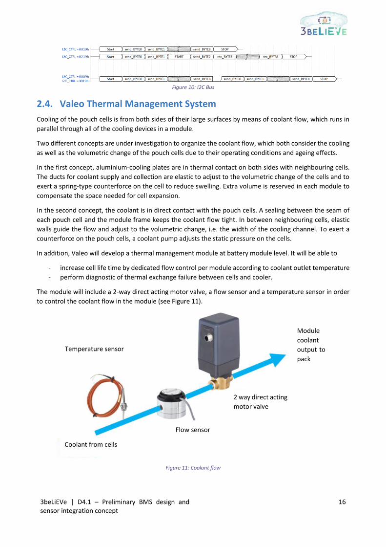
The module will include a 2-way direct acting motor valve, a flow sensor and a temperature sensor in order
to control the coolant flow in the module (see Figure 11).
Figure 11: Coolant flow
Temperature sensor
Flow sensor
2 way direct acting
motor valve
Module
coolant
output to
pack
Coolant from cells

3beLiEVe | D4.1 – Preliminary BMS design and sensor integration concept
17
The module will have two different operating modes with a dedicated control strategy:
1. “Smart” management deactivated → fixed position @ nominal flow
2. “Smart” management activated → variable position following flow map, function of coolant
temperature module outlet and coolant temperature pack outlet)
The diagnostic of the thermal exchange “quality” will be performed with a continuous calculation of the
thermal exchange level function of coolant flow, pack inlet temperature and module outlet temperature
(see Figure 12).
Figure 12: Block diagram of the coolant flow
Current investigation shows that the complete control will be integrated through an Arduino device
connected to the BMS with SPI bus.
Thermal Management Module
Module outlet Tcoolant temperature
Pack inlet Tcoolant temperature
Coolant flow
3beLiEVe | D4.1 – Preliminary BMS design and sensor integration concept
18
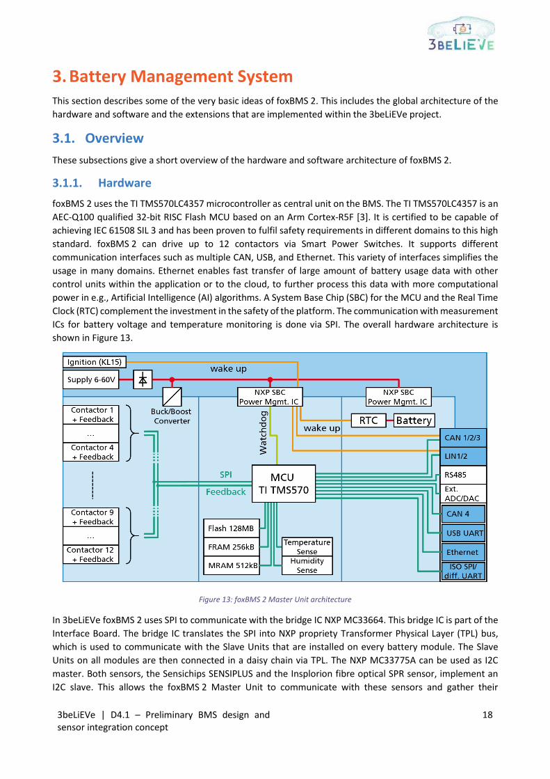
3. Battery Management System This section describes some of the very basic ideas of foxBMS 2. This includes the global architecture of the
hardware and software and the extensions that are implemented within the 3beLiEVe project.
3.1. Overview
These subsections give a short overview of the hardware and software architecture of foxBMS 2.
3.1.1. Hardware
foxBMS 2 uses the TI TMS570LC4357 microcontroller as central unit on the BMS. The TI TMS570LC4357 is an
AEC-Q100 qualified 32-bit RISC Flash MCU based on an Arm Cortex-R5F [3]. It is certified to be capable of
achieving IEC 61508 SIL 3 and has been proven to fulfil safety requirements in different domains to this high
standard. foxBMS 2 can drive up to 12 contactors via Smart Power Switches. It supports different
communication interfaces such as multiple CAN, USB, and Ethernet. This variety of interfaces simplifies the
usage in many domains. Ethernet enables fast transfer of large amount of battery usage data with other
control units within the application or to the cloud, to further process this data with more computational
power in e.g., Artificial Intelligence (AI) algorithms. A System Base Chip (SBC) for the MCU and the Real Time
Clock (RTC) complement the investment in the safety of the platform. The communication with measurement
ICs for battery voltage and temperature monitoring is done via SPI. The overall hardware architecture is
shown in Figure 13.
Figure 13: foxBMS 2 Master Unit architecture
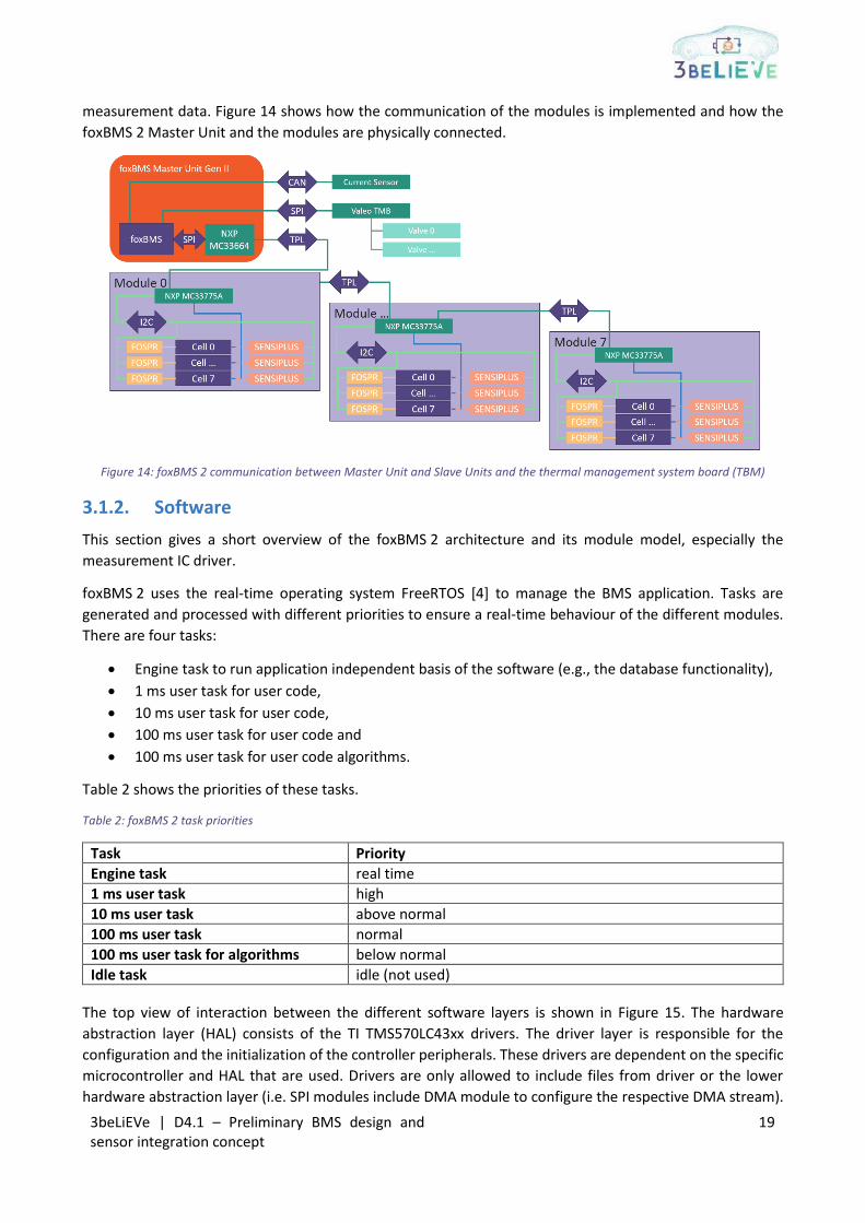
In 3beLiEVe foxBMS 2 uses SPI to communicate with the bridge IC NXP MC33664. This bridge IC is part of the
Interface Board. The bridge IC translates the SPI into NXP propriety Transformer Physical Layer (TPL) bus,
which is used to communicate with the Slave Units that are installed on every battery module. The Slave
Units on all modules are then connected in a daisy chain via TPL. The NXP MC33775A can be used as I2C
master. Both sensors, the Sensichips SENSIPLUS and the Insplorion fibre optical SPR sensor, implement an
I2C slave. This allows the foxBMS 2 Master Unit to communicate with these sensors and gather their
3beLiEVe | D4.1 – Preliminary BMS design and sensor integration concept
19
measurement data. Figure 14 shows how the communication of the modules is implemented and how the
foxBMS 2 Master Unit and the modules are physically connected.
Figure 14: foxBMS 2 communication between Master Unit and Slave Units and the thermal management system board (TBM)
3.1.2. Software
This section gives a short overview of the foxBMS 2 architecture and its module model, especially the
measurement IC driver.
foxBMS 2 uses the real-time operating system FreeRTOS [4] to manage the BMS application. Tasks are
generated and processed with different priorities to ensure a real-time behaviour of the different modules.
There are four tasks:
• Engine task to run application independent basis of the software (e.g., the database functionality),
• 1 ms user task for user code,
• 10 ms user task for user code,
• 100 ms user task for user code and
• 100 ms user task for user code algorithms.
Table 2 shows the priorities of these tasks.
Table 2: foxBMS 2 task priorities
Task Priority
Engine task real time
1 ms user task high
10 ms user task above normal
100 ms user task normal
100 ms user task for algorithms below normal
Idle task idle (not used)
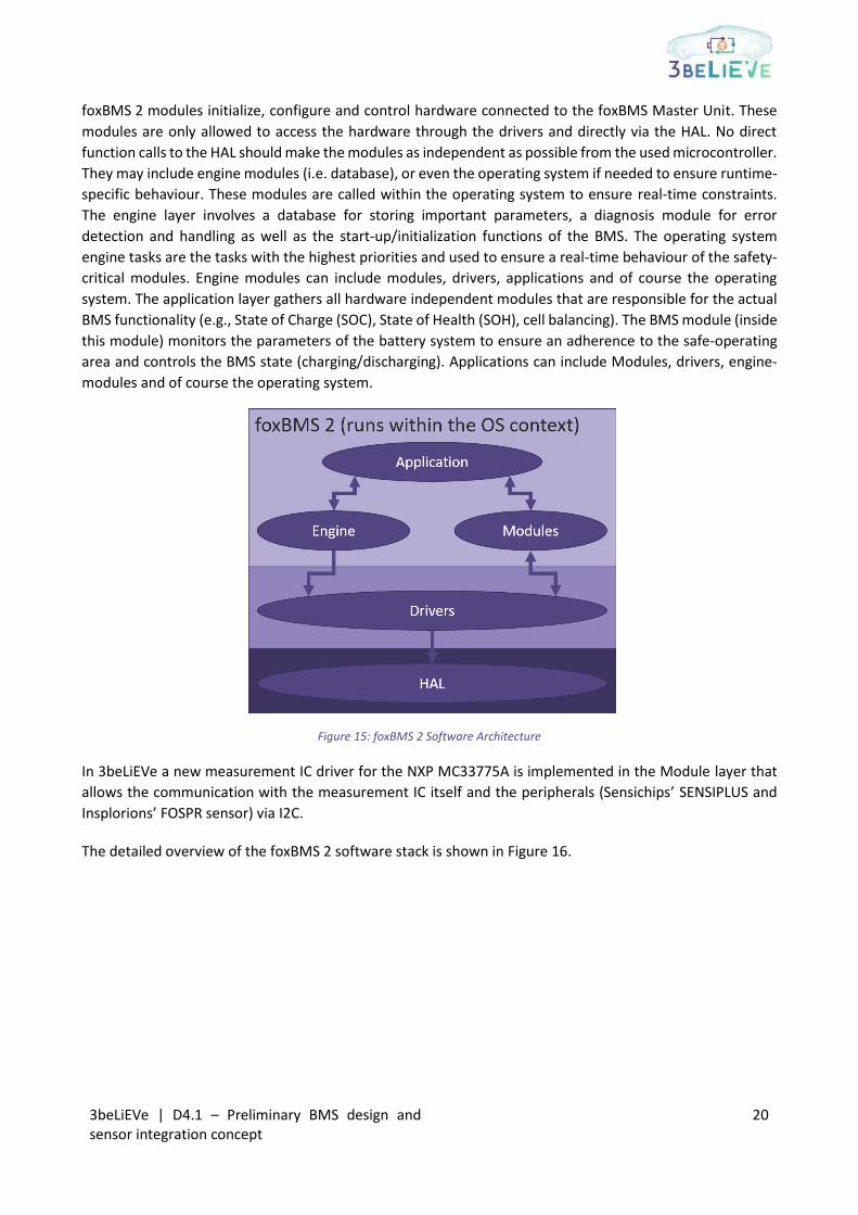
The top view of interaction between the different software layers is shown in Figure 15. The hardware
abstraction layer (HAL) consists of the TI TMS570LC43xx drivers. The driver layer is responsible for the
configuration and the initialization of the controller peripherals. These drivers are dependent on the specific
microcontroller and HAL that are used. Drivers are only allowed to include files from driver or the lower
hardware abstraction layer (i.e. SPI modules include DMA module to configure the respective DMA stream).
3beLiEVe | D4.1 – Preliminary BMS design and sensor integration concept
20
foxBMS 2 modules initialize, configure and control hardware connected to the foxBMS Master Unit. These
modules are only allowed to access the hardware through the drivers and directly via the HAL. No direct
function calls to the HAL should make the modules as independent as possible from the used microcontroller.
They may include engine modules (i.e. database), or even the operating system if needed to ensure runtime-
specific behaviour. These modules are called within the operating system to ensure real-time constraints.
The engine layer involves a database for storing important parameters, a diagnosis module for error
detection and handling as well as the start-up/initialization functions of the BMS. The operating system
engine tasks are the tasks with the highest priorities and used to ensure a real-time behaviour of the safety-
critical modules. Engine modules can include modules, drivers, applications and of course the operating
system. The application layer gathers all hardware independent modules that are responsible for the actual
BMS functionality (e.g., State of Charge (SOC), State of Health (SOH), cell balancing). The BMS module (inside
this module) monitors the parameters of the battery system to ensure an adherence to the safe-operating
area and controls the BMS state (charging/discharging). Applications can include Modules, drivers, engine-
modules and of course the operating system.
Figure 15: foxBMS 2 Software Architecture
In 3beLiEVe a new measurement IC driver for the NXP MC33775A is implemented in the Module layer that
allows the communication with the measurement IC itself and the peripherals (Sensichips’ SENSIPLUS and
Insplorions’ FOSPR sensor) via I2C.
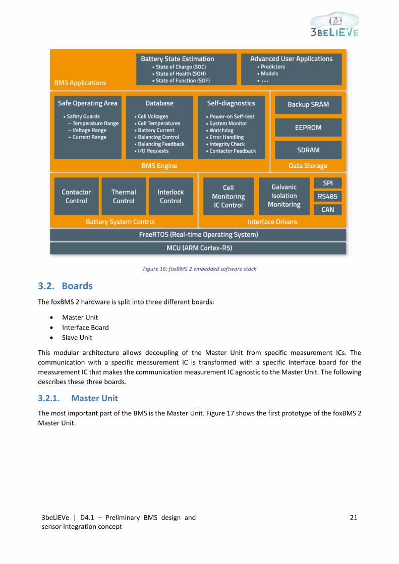
The detailed overview of the foxBMS 2 software stack is shown in Figure 16.
3beLiEVe | D4.1 – Preliminary BMS design and sensor integration concept
21
Figure 16: foxBMS 2 embedded software stack
3.2. Boards
The foxBMS 2 hardware is split into three different boards:
• Master Unit
• Interface Board
• Slave Unit
This modular architecture allows decoupling of the Master Unit from specific measurement ICs. The
communication with a specific measurement IC is transformed with a specific Interface board for the
measurement IC that makes the communication measurement IC agnostic to the Master Unit. The following
describes these three boards.
3.2.1. Master Unit
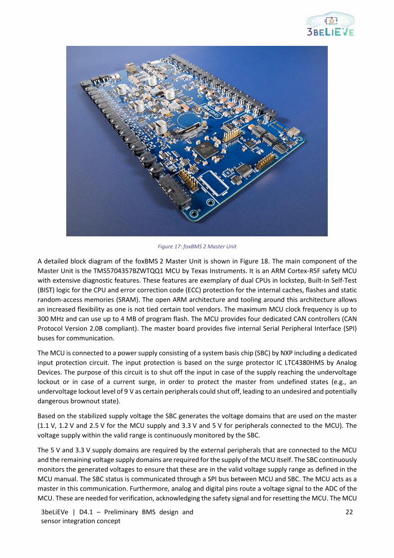
The most important part of the BMS is the Master Unit. Figure 17 shows the first prototype of the foxBMS 2
Master Unit.
3beLiEVe | D4.1 – Preliminary BMS design and sensor integration concept
22
Figure 17: foxBMS 2 Master Unit
A detailed block diagram of the foxBMS 2 Master Unit is shown in Figure 18. The main component of the
Master Unit is the TMS5704357BZWTQQ1 MCU by Texas Instruments. It is an ARM Cortex-R5F safety MCU
with extensive diagnostic features. These features are exemplary of dual CPUs in lockstep, Built-In Self-Test
(BIST) logic for the CPU and error correction code (ECC) protection for the internal caches, flashes and static
random-access memories (SRAM). The open ARM architecture and tooling around this architecture allows
an increased flexibility as one is not tied certain tool vendors. The maximum MCU clock frequency is up to
300 MHz and can use up to 4 MB of program flash. The MCU provides four dedicated CAN controllers (CAN
Protocol Version 2.0B compliant). The master board provides five internal Serial Peripheral Interface (SPI)
buses for communication.
The MCU is connected to a power supply consisting of a system basis chip (SBC) by NXP including a dedicated
input protection circuit. The input protection is based on the surge protector IC LTC4380HMS by Analog
Devices. The purpose of this circuit is to shut off the input in case of the supply reaching the undervoltage
lockout or in case of a current surge, in order to protect the master from undefined states (e.g., an
undervoltage lockout level of 9 V as certain peripherals could shut off, leading to an undesired and potentially
dangerous brownout state).
Based on the stabilized supply voltage the SBC generates the voltage domains that are used on the master
(1.1 V, 1.2 V and 2.5 V for the MCU supply and 3.3 V and 5 V for peripherals connected to the MCU). The
voltage supply within the valid range is continuously monitored by the SBC.
The 5 V and 3.3 V supply domains are required by the external peripherals that are connected to the MCU
and the remaining voltage supply domains are required for the supply of the MCU itself. The SBC continuously
monitors the generated voltages to ensure that these are in the valid voltage supply range as defined in the
MCU manual. The SBC status is communicated through a SPI bus between MCU and SBC. The MCU acts as a
master in this communication. Furthermore, analog and digital pins route a voltage signal to the ADC of the
MCU. These are needed for verification, acknowledging the safety signal and for resetting the MCU. The MCU

3beLiEVe | D4.1 – Preliminary BMS design and sensor integration concept
23
and SBC are connected through SPI2. The MCU is strictly required to continuously trigger the watchdog
routine in the SBC. If the MCU fails to perform this task, the SBC assumes an error in the embedded software
execution on the MCU and triggers a reset.
Figure 18: Block diagram of the foxBMS 2 master
The safety design of the foxBMS 2 platform does not only take into account the MCU and the SBC, but also
improves the safety of all other components like the oscillator, for example. The oscillator generates a stable
clock for the MCU. Oscillator failures can lead to a non-deterministic system behaviour. Quartz-based
oscillators are the typical choice for such applications but they have a mean time between failures (MTBF) of
1 to 38 million hours. The selected MEMS oscillator (SITime SIT8924BM-31) has a targeted MTBF of 500
million hours. foxBMS 2 uses a programmed frequency of 20 MHz.
In addition to the watchdog in the SBC, foxBMS 2 also features a window watchdog (Maxim Integrated
MAX16998DAUA/V+). A standard watchdog implementation checks if it has been triggered at least once in a
certain timeframe. A window watchdog improves safety, as it requires a precise timing for its triggering. A
window watchdog prevents errors where the software would service the watchdog in an endless loop in
which it just continuously triggers the watchdog as fast as possible.
foxBMS 2 features non-volatile ferroelectric RAM (FRAM) to store data persistently, for example operating
hours or under- and overvoltage violations (Cypress CY15B102QN-50SXE). This type of non-volatile memory
has been chosen as it has the advantage of a virtually infinite number of read/write cycles.
A CAN-interface implementation is shown in Figure 19. The CAN-interface can be isolated from the Master
Unit and powered externally or powered internally. External power supplies can be used in order to wake up
the Master Unit over a CAN-message, if the CAN-transceiver is connected through its interrupt line to the
MCU. The isolation of the CAN-interface is achieved through the digital isolator TI's ISO7763FQDWQ1, which
Isolated Isolated IsolatedIsolated (each
isoSPI separately)Isolated (each
isoSPI separately)Isolated
Supplied by SBC
MCUTMS5704357BZWTQQ1
WWDGMAX16998
FRAMCY15B102QN-
50SXE
OscillatorSIT8924BM
SBCInput
ProtectionLTC4380HMS
clock
Protectedsupply
SPI2
ADC values
Safety signal
WDI
Reset
Reset
SPI3
IsolatedCAN-
Interface
IsolatedCAN-
Interface
IsolatedCAN-
Interface
IsolatedCAN-
Interface
3x Isolated isoSPI
Interface
3x Isolated isoSPI
Interface
CAN1
CAN2CAN3
CAN4SPI1
SPI4
3beLiEVe | D4.1 – Preliminary BMS design and sensor integration concept
24
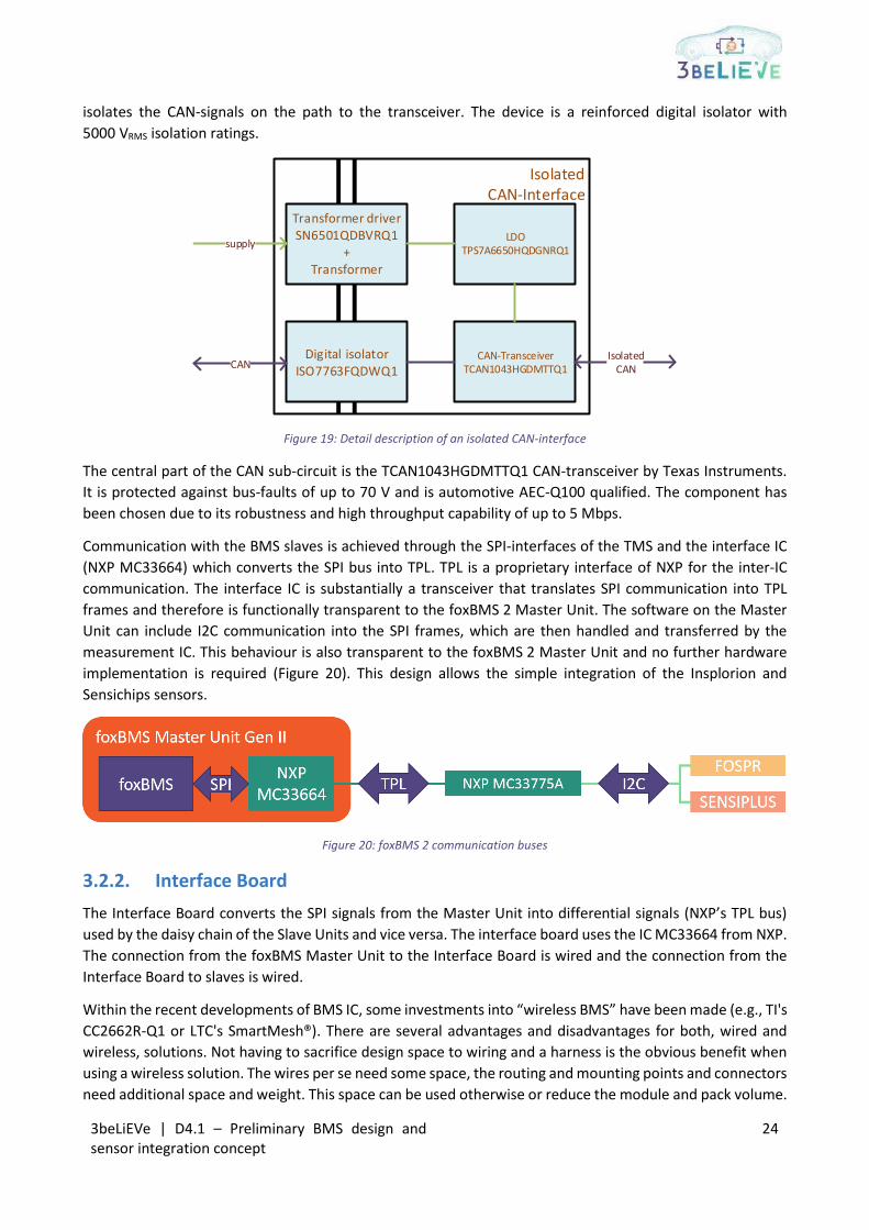
isolates the CAN-signals on the path to the transceiver. The device is a reinforced digital isolator with
5000 VRMS isolation ratings.
Figure 19: Detail description of an isolated CAN-interface
The central part of the CAN sub-circuit is the TCAN1043HGDMTTQ1 CAN-transceiver by Texas Instruments.
It is protected against bus-faults of up to 70 V and is automotive AEC-Q100 qualified. The component has
been chosen due to its robustness and high throughput capability of up to 5 Mbps.
Communication with the BMS slaves is achieved through the SPI-interfaces of the TMS and the interface IC
(NXP MC33664) which converts the SPI bus into TPL. TPL is a proprietary interface of NXP for the inter-IC
communication. The interface IC is substantially a transceiver that translates SPI communication into TPL
frames and therefore is functionally transparent to the foxBMS 2 Master Unit. The software on the Master
Unit can include I2C communication into the SPI frames, which are then handled and transferred by the
measurement IC. This behaviour is also transparent to the foxBMS 2 Master Unit and no further hardware
implementation is required (Figure 20). This design allows the simple integration of the Insplorion and
Sensichips sensors.
Figure 20: foxBMS 2 communication buses
3.2.2. Interface Board
The Interface Board converts the SPI signals from the Master Unit into differential signals (NXP’s TPL bus)
used by the daisy chain of the Slave Units and vice versa. The interface board uses the IC MC33664 from NXP.
The connection from the foxBMS Master Unit to the Interface Board is wired and the connection from the
Interface Board to slaves is wired.
Within the recent developments of BMS IC, some investments into “wireless BMS” have been made (e.g., TI's
CC2662R-Q1 or LTC's SmartMesh®). There are several advantages and disadvantages for both, wired and
wireless, solutions. Not having to sacrifice design space to wiring and a harness is the obvious benefit when
using a wireless solution. The wires per se need some space, the routing and mounting points and connectors
need additional space and weight. This space can be used otherwise or reduce the module and pack volume.
IsolatedCAN-Interface
LDOTPS7A6650HQDGNRQ1
CAN-TransceiverTCAN1043HGDMTTQ1
Transformer driverSN6501QDBVRQ1
+Transformer
Digital isolatorISO7763FQDWQ1
supply
CANIsolated
CAN

3beLiEVe | D4.1 – Preliminary BMS design and sensor integration concept
25
From a mechanical point of view, the maintainability of a wireless solution is also better, as broken wires are
no longer a point of concern. In reality, broken communication wires in battery-powered applications have
not shown to be a major point of concern. A wireless BMS can synchronously communicate with all
measurement ICs, which gives it an obvious advantage compared to a daisy-chained wired solution where
the delay in the daisy chain must be taken into account. However, the number of measurement ICs connected
in daisy-chain have not shown to be a problem in real-world applications, as there are options to overcome
this problem (e.g. using different SPIs and parallelizing the measurement). The wired solutions already fulfil
functional safety standards and are used in most currently available BEVs and other battery-powered
solutions, while wireless solutions still need to prove that they work reliably in harsh environments in terms
of radio-frequency and interference. Furthermore, non-line-of-sight might be a problem of the wireless
communication and designing a solution to not face this problem might reduce the savings in volume.
Another problem of the wireless solution is that it needs to be safe in terms of security. A wired solution
within a sealed battery module and pack is secure against data manipulation, while the wireless solution
opens a new way of tampering with safety critical data.
For the 3beLiEVe project, where the initial integration of the sensors and the reliable transfer of the sensor-
generated data for algorithm development is one of the key points of the project, the wired solution is more
suitable. The drawbacks in term of design flexibility of modules and pack have shown to be not significant
within the project. Therefore, the “wired BMS” solution has been chosen.
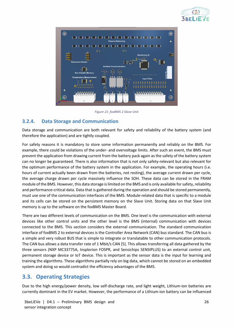
3.2.3. Slave Units
The foxBMS 2 Slave Unit includes the NXP MC33557A as a main feature, as this is measurement IC performing
the high accuracy and safety-relevant voltage and temperature monitoring. The Slave unit features up to 14
cell voltages and 8 temperatures that can be monitored. The Slave Unit supports passive balancing up to
300 mA. The isolator for the communication line connecting the Slave Unit to the master shall withstand
minimum 1000 VDC continuously for the lifetime of the application. The Slave Board enables the
communication with the sensors via the I2C bus. The I2C bus of the NXP MC33775A has a maximum bus
frequency of 400 kHz and should use a 3.3 V bus voltage. The Insplorion hardware is featured on the Slave
Unit and supplied by the Slave Unit through an extension header. The Slave Board includes a further bridge
IC to communicate with the Sensichips as it implements a proprietary protocol. The communication with the
bridge IC is also performed via I2C. The I2C communication with the bridge IC does not need to be isolated
as the I2C isolation is done on the Sensichips SENSIPLUS IC. The Slave Board must provide a total of 120 mA
supply for the NXP MC33775A, the Insplorion FOSPR and the Sensichips SENSIPLUS. The NXP measurement
IC must be supplied with 5 V, and Insplorion FOSPR and the bridge IC with 3.3 V. To store safety and second-
life-related data on the Slave Board pertaining to the module it is mounted to, each Slave Board is fitted with
a memory component for this persistent storage. Figure 21 shows the design of the foxBMS 2 Slave Unit.
3beLiEVe | D4.1 – Preliminary BMS design and sensor integration concept
26
Figure 21: foxBMS 2 Slave Unit
3.2.4. Data Storage and Communication
Data storage and communication are both relevant for safety and reliability of the battery system (and
therefore the application) and are tightly coupled.
For safety reasons it is mandatory to store some information permanently and reliably on the BMS. For
example, there could be violations of the under- and overvoltage limits. After such an event, the BMS must
prevent the application from drawing current from the battery pack again as the safety of the battery system
can no longer be guaranteed. There is also information that is not only safety-relevant but also relevant for
the optimum performance of the battery system in the application. For example, the operating hours (i.e.
hours of current actually been drawn from the batteries, not resting), the average current drawn per cycle,
the average charge drawn per cycle massively influence the SOH. These data can be stored in the FRAM
module of the BMS. However, this data storage is limited on the BMS and is only available for safety, reliability
and performance-critical data. Data that is gathered during the operation and should be stored permanently,
must use one of the communication interfaces of the BMS. Module-related data that is specific to a module
and its cells can be stored on the persistent memory on the Slave Unit. Storing data on that Slave Unit
memory is up to the software on the foxBMS Master Board.
There are two different levels of communication on the BMS. One level is the communication with external
devices like other control units and the other level is the BMS (internal) communication with devices
connected to the BMS. This section considers the external communication. The standard communication
interface of foxBMS 2 to external devices is the Controller Area Network (CAN) bus standard. The CAN bus is
a simple and very robust BUS that is simple to integrate or translatable to other communication protocols.
The CAN bus allows a data transfer rate of 1 Mbit/s CAN [5]. This allows transferring all data gathered by the
three sensors (NXP MC33775A, Insplorion FOSPR, and Sensichips SENSIPLUS) to an external control unit,
permanent storage device or IoT device. This is important as the sensor data is the input for learning and
training the algorithms. These algorithms partially rely on big data, which cannot be stored on an embedded
system and doing so would contradict the efficiency advantages of the BMS.
3.3. Operating Strategies
Due to the high energy/power density, low self-discharge rate, and light weight, Lithium-ion batteries are
currently dominant in the EV market. However, the performance of a Lithium-ion battery can be influenced
3beLiEVe | D4.1 – Preliminary BMS design and sensor integration concept
27
by usage patterns, temperature, current rate, as well as ageing. Therefore, special attention should be given
to operating conditions to avoid any potential damage, thermal runaway, ageing,
overcharging/overdischarging, and so on. In general, the battery management system (BMS) needs to
monitor battery voltage, current, and temperature to properly control components such as charger, cooling
system, heater, and balancer.
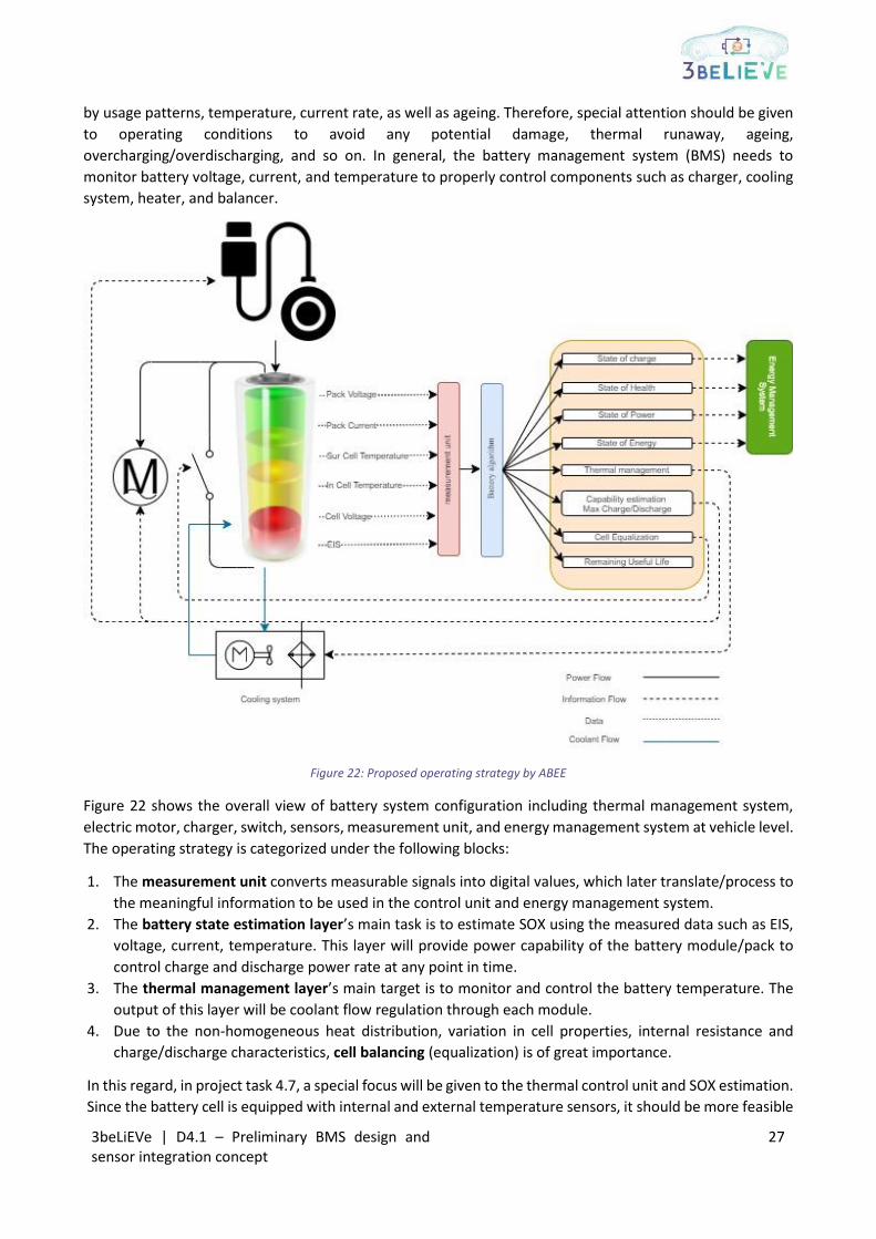
Figure 22: Proposed operating strategy by ABEE
Figure 22 shows the overall view of battery system configuration including thermal management system,
electric motor, charger, switch, sensors, measurement unit, and energy management system at vehicle level.
The operating strategy is categorized under the following blocks:
1. The measurement unit converts measurable signals into digital values, which later translate/process to
the meaningful information to be used in the control unit and energy management system.
2. The battery state estimation layer’s main task is to estimate SOX using the measured data such as EIS,
voltage, current, temperature. This layer will provide power capability of the battery module/pack to
control charge and discharge power rate at any point in time.
3. The thermal management layer’s main target is to monitor and control the battery temperature. The
output of this layer will be coolant flow regulation through each module.
4. Due to the non-homogeneous heat distribution, variation in cell properties, internal resistance and
charge/discharge characteristics, cell balancing (equalization) is of great importance.
In this regard, in project task 4.7, a special focus will be given to the thermal control unit and SOX estimation.
Since the battery cell is equipped with internal and external temperature sensors, it should be more feasible
3beLiEVe | D4.1 – Preliminary BMS design and sensor integration concept
28
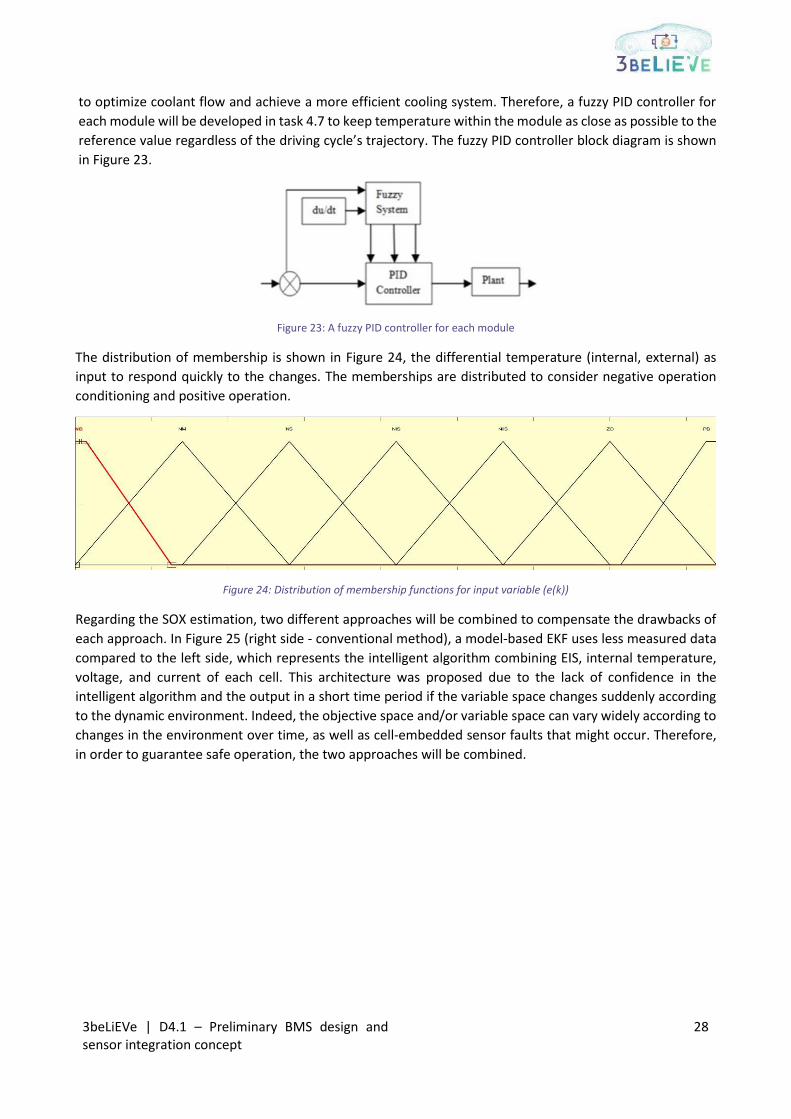
to optimize coolant flow and achieve a more efficient cooling system. Therefore, a fuzzy PID controller for
each module will be developed in task 4.7 to keep temperature within the module as close as possible to the
reference value regardless of the driving cycle’s trajectory. The fuzzy PID controller block diagram is shown
in Figure 23.
Figure 23: A fuzzy PID controller for each module
The distribution of membership is shown in Figure 24, the differential temperature (internal, external) as
input to respond quickly to the changes. The memberships are distributed to consider negative operation
conditioning and positive operation.
Figure 24: Distribution of membership functions for input variable (e(k))
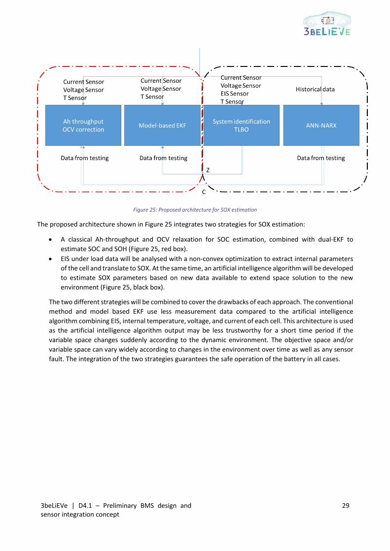
Regarding the SOX estimation, two different approaches will be combined to compensate the drawbacks of
each approach. In Figure 25 (right side - conventional method), a model-based EKF uses less measured data
compared to the left side, which represents the intelligent algorithm combining EIS, internal temperature,
voltage, and current of each cell. This architecture was proposed due to the lack of confidence in the
intelligent algorithm and the output in a short time period if the variable space changes suddenly according
to the dynamic environment. Indeed, the objective space and/or variable space can vary widely according to
changes in the environment over time, as well as cell-embedded sensor faults that might occur. Therefore,
in order to guarantee safe operation, the two approaches will be combined.
3beLiEVe | D4.1 – Preliminary BMS design and sensor integration concept
29
Figure 25: Proposed architecture for SOX estimation
The proposed architecture shown in Figure 25 integrates two strategies for SOX estimation:
• A classical Ah-throughput and OCV relaxation for SOC estimation, combined with dual-EKF to
estimate SOC and SOH (Figure 25, red box).
• EIS under load data will be analysed with a non-convex optimization to extract internal parameters
of the cell and translate to SOX. At the same time, an artificial intelligence algorithm will be developed
to estimate SOX parameters based on new data available to extend space solution to the new
environment (Figure 25, black box).
The two different strategies will be combined to cover the drawbacks of each approach. The conventional
method and model based EKF use less measurement data compared to the artificial intelligence
algorithm combining EIS, internal temperature, voltage, and current of each cell. This architecture is used
as the artificial intelligence algorithm output may be less trustworthy for a short time period if the
variable space changes suddenly according to the dynamic environment. The objective space and/or
variable space can vary widely according to changes in the environment over time as well as any sensor
fault. The integration of the two strategies guarantees the safe operation of the battery in all cases.
3beLiEVe | D4.1 – Preliminary BMS design and sensor integration concept
30
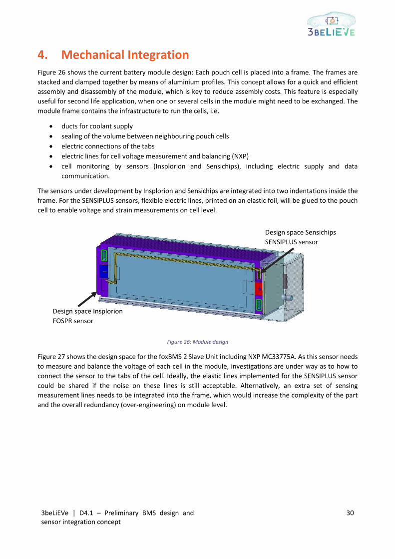
4. Mechanical Integration Figure 26 shows the current battery module design: Each pouch cell is placed into a frame. The frames are
stacked and clamped together by means of aluminium profiles. This concept allows for a quick and efficient
assembly and disassembly of the module, which is key to reduce assembly costs. This feature is especially
useful for second life application, when one or several cells in the module might need to be exchanged. The
module frame contains the infrastructure to run the cells, i.e.
• ducts for coolant supply
• sealing of the volume between neighbouring pouch cells
• electric connections of the tabs
• electric lines for cell voltage measurement and balancing (NXP)
• cell monitoring by sensors (Insplorion and Sensichips), including electric supply and data
communication.
The sensors under development by Insplorion and Sensichips are integrated into two indentations inside the
frame. For the SENSIPLUS sensors, flexible electric lines, printed on an elastic foil, will be glued to the pouch
cell to enable voltage and strain measurements on cell level.
Figure 26: Module design
Figure 27 shows the design space for the foxBMS 2 Slave Unit including NXP MC33775A. As this sensor needs
to measure and balance the voltage of each cell in the module, investigations are under way as to how to
connect the sensor to the tabs of the cell. Ideally, the elastic lines implemented for the SENSIPLUS sensor
could be shared if the noise on these lines is still acceptable. Alternatively, an extra set of sensing
measurement lines needs to be integrated into the frame, which would increase the complexity of the part
and the overall redundancy (over-engineering) on module level.
Design space Insplorion
FOSPR sensor
Design space Sensichips
SENSIPLUS sensor

3beLiEVe | D4.1 – Preliminary BMS design and sensor integration concept
31
Figure 27: Design space for the foxBMS 2 NXP slave board
5. Conclusions This document provided a first overview of the BMS design of foxBM2 in the context of the 3beLiEVe project.
It described the rationale behind the development of foxBM2 and described the system itself in detail.
Furthermore, it showed the concept for integrating the selected sensors with the BMS from a communication
perspective, as well as the integration concept for the BMS and sensors into the battery module from a
mechanical/hardware perspective.
A battery system that is configurable to the respective application can be controlled with the second
generation of foxBMS. foxBMS 2 enables rapid prototyping with the safety of a later product already in mind,
by using cutting-edge components and by implementing drivers for safety-certified measurement ICs like the
NXP MC33775A. Innovative sensors, such as the Insplorion FOSPR, which are integrated at battery cell level,
provide valuable input for SOX estimation to the BMS, to enable an optimal runtime and lifetime operation
of the battery system and therefore of the battery-powered application. Highly integrated sensors like the
Sensichips SENSIPLUS sensor will contribute to SOX estimation with its EIS sensor and provide further safety-
relevant information, e.g., about gassing and strain, to further ensure a maximum level of safety. The
acquired sensor data can be streamed to an external device through the communication interfaces of the
BMS and be analysed further. Based on these learnings better operating strategies can be found. The
resulting operating strategies are brought back into the BMS, to ensure a safe and optimal operation of the
battery-powered application. This deliverable outlined those operating strategies. Two different strategies
are combined to compensate the drawbacks of each individual strategy. The more traditional EKF approach
uses less data, while the AI-enabled approach uses additional data acquired by the sensors integrated on cell
and module level.
Finally, the information outlined here will be further detailed during the project in the following deliverables.
D4.2 will describe the final design of the sensors. D4.3 will describe the adaptive cooling systems and the
final BMS design, and D4.4 will detail the advanced diagnostics and the adaptive operating strategy. The final
design and specifications of module and pack will be given in D6.2.
Design space foxBMS 2
Slave Unit including NXP
MC33775A
Sense wiring
Battery terminal Cooling inlet
Battery cell (Pouch,
Custom Cells
Itzehoe)
3beLiEVe | D4.1 – Preliminary BMS design and sensor integration concept
32
References
[1] Fraunhofer IISB, “foxbms.org,” 01 03 2021. [Online]. Available: https://foxbms.org. [Accessed 01 03
2021].
[2] Fraunhofer IISB, “foxbms-2,” 01 04 2021. [Online]. Available: https://www.github.com/foxBMS/foxbms-
2. [Accessed 01 04 2021].
[3] Texas Instruments Incorporated, “TMS570LC4357,” 01 03 2021. [Online]. Available:
https://www.ti.com/product/TMS570LC4357. [Accessed 01 03 2021].
[4] Amazon Web Services, [Online]. Available: https://freertos.org/. [Accessed 16 02 2021].
[5] International Organization for Standardization, “ISO 11898-2”.

3beLiEVe | D4.1 – Preliminary BMS design and sensor integration concept
33
This project has received funding from the European Union’s H2020 research and innovation programme under Grant Agreement no. 875033.
This publication reflects only the author’s view and the Innovation
and Networks Executive Agency (INEA) is not responsible for any use
that may be made of the information it contains.